cc2640 simplelink bluetooth smart wireless mcu€¢ ultra-low power sensor controller –...
TRANSCRIPT
Product
Folder
Sample &Buy
Technical
Documents
Tools &
Software
Support &Community
CC2640SWRS176 –FEBRUARY 2015
CC2640 SimpleLink™ Bluetooth® Smart Wireless MCU1 Device Overview
1.1 Features1
– Very Few External Components• Microcontroller– Seamless Integration With the SimpleLink– Powerful ARM® Cortex®-M3
CC2590 and CC2592 Range Extenders– EEMBC CoreMark® score: 142– Pin Compatible With the SimpleLink CC13xx in– Up to 48-MHz Clock Speed
4-mm × 4-mm and 5-mm × 5-mm QFN– 128KB of In-System Programmable Flash Packages– 8-KB SRAM for Cache • Low Power– 20-KB Ultra-Low Leakage SRAM – Wide Supply Voltage Range– 2-Pin cJTAG and JTAG Debugging • Normal Operation: 1.8 to 3.8 V– Supports Over-The-Air Upgrade (OTA) • External Regulator Mode: 1.7 to 1.95 V• Ultra-Low Power Sensor Controller – Active-mode RX: 5.9 mA– Can run autonomous from the rest of the – Active-mode TX at 0 dBm: 6.1 mAsystem
– Active-mode TX at +5 dBm: 9.1 mA– 16-Bit Architecture– Active-mode MCU: 61 µA/MHz– 2-KB Ultra-Low Leakage SRAM for Code and– Active-mode MCU: 48.5 CoreMark/mAData– Active-mode Sensor Controller: 8.2 µA/MHz• Efficient Code Size Architecture, Placing Drivers,– Standby: 1 µA (RTC Running and RAM/CPUBluetooth® Low Energy Controller, and Bootloader
Retention)in ROM– Shutdown: 100 nA (Wake-up on External• RoHS-Compliant Packages
Events)– 4-mm × 4-mm RSM QFN32 (10 GPIOs)• RF Section– 5-mm × 5-mm RHB QFN32 (15 GPIOs)
– 2.4 GHz RF Transceiver Compatible With– 7-mm x 7-mm RGZ QFN48 (31 GPIOs)Bluetooth Low Energy (BLE) 4.1 specification• Peripherals
– Excellent Receiver Sensitivity (–97 dBm for– All Digital Peripheral Pins can be Routed to any BLE), Selectivity, and Blocking PerformanceGPIO– Programmable Output Power up to +5 dBm– 4 General-Purpose Timer Modules (8 × 16-Bit or– Single-ended or Differential RF Interface4 × 32-Bit Timer, PWM Each)– Suitable for Systems Targeting Compliance With– 12-Bit ADC, 200-ksamples/s, 8-Channel Analog
Worldwide Radio Frequency RegulationsMUX• ETSI EN 300 328 (Europe)– Continuous Time Comparator• EN 300 440 Class 2 (Europe)– Ultra-Low Power Analog Comparator• FCC CFR47 Part 15 (US)– Programmable Current Source• ARIB STD-T66 (Japan)– UART
• Tools and Development Environment– 2x SSI (SPI, µW, TI)– Full-Feature and Low-Cost Development Kits– I2C– Multiple Reference Designs for Different RF– I2S
Configurations– Real-Time Clock (RTC)– Packet Sniffer PC Software– AES-128 Security Module– Sensor Controller Studio– True Random Number Generator (TRNG)– SmartRF™ Studio– 10, 15, or 31 GPIOs, Depending on Package– SmartRF Flash Programmer 2Option– IAR Embedded Workbench® for ARM– Support for 8 Capacitive Sensing Buttons– Code Composer Studio™– Integrated Temperature Sensor
• External System– On-Chip internal DC-DC Converter
1
An IMPORTANT NOTICE at the end of this data sheet addresses availability, warranty, changes, use in safety-critical applications,intellectual property matters and other important disclaimers. PRODUCTION DATA.
CC2640SWRS176 –FEBRUARY 2015 www.ti.com
1.2 Applications• Home and Building Automation • Health and Medical
– Connected Appliances – Thermometers– Lighting – SpO2– Locks – Blood Glucose and Pressure Meters– Gateways – Weight-scales– Security Systems – Vitals Monitoring
– Hearing Aids• Industrial– Logistics • Sports and Fitness– Production and Manufacturing – Activity Monitors and Fitness Trackers– Automation – Heart Rate Monitors– Asset Tracking and Management – Running Sensors– Remote Display – Biking Sensors– Cable Replacement – Sports Watches– HMI – Gym Equipment– Access Control – Team Sports Equipment
• Retail • HID– Beacons – Remote Controls– Advertising – Keyboards and Mice– ESL / Price Tags – Gaming– Point of Sales / Payment Systems • Accessories
– Toys– Trackers– Luggage-tags– Wearables
1.3 DescriptionThe CC2640 is a wireless MCU targeting Bluetooth Smart applications.
The device is a member of the CC26xx family of cost-effective, ultra-low power, 2.4-GHz RF devices. Verylow active RF and MCU current, and low-power mode current consumption provides excellent batterylifetime and allows operation on small coin cell batteries and in energy-harvesting applications.
The CC2640 contains a 32-bit ARM Cortex-M3 running at 48-MHz as the main processor and a richperipheral feature set, including a unique ultra-low power sensor controller, ideal for interfacing externalsensors and/or collecting analog and digital data autonomously while the rest of the system is in sleepmode.
This makes the CC2640 ideal for a wide range of applications where long battery lifetime, small formfactor, and ease of use is important.
The Bluetooth Low Energy controller is embedded into ROM and run partly on an ARM Cortex®-M0processor. This architecture improves overall system performance and power consumption and frees upflash memory for the application.
The Bluetooth Smart stack is available free of charge from www.ti.com.
Device Information (1)
PART NUMBER PACKAGE BODY SIZECC2640F128RGZ RGZ (QFN48) 7.00 mm × 7.00 mmCC2640F128RHB RHB (QFN32) 5.00 mm × 5.00 mm
(1) For more information, see Section 9, Mechanical Packaging and Orderable Information.
2 Device Overview Copyright © 2015, Texas Instruments IncorporatedSubmit Documentation Feedback
Product Folder Links: CC2640

CC2640www.ti.com SWRS176 –FEBRUARY 2015
Device Information(1) (continued)PART NUMBER PACKAGE BODY SIZE
CC2640F128RSM RSM (QFN32) 4.00 mm × 4.00 mm
Copyright © 2015, Texas Instruments Incorporated Device Overview 3Submit Documentation Feedback
Product Folder Links: CC2640

CC2640SWRS176 –FEBRUARY 2015 www.ti.com
1.4 Functional Block DiagramSection 1.4 shows a block diagram for the CC2640.
Figure 1-1. Block Diagram
4 Device Overview Copyright © 2015, Texas Instruments IncorporatedSubmit Documentation Feedback
Product Folder Links: CC2640

CC2640www.ti.com SWRS176 –FEBRUARY 2015
Table of Contents1 Device Overview ......................................... 1 5.16 Battery Monitor ...................................... 19
1.1 Features .............................................. 1 5.17 Continuous Time Comparator....................... 201.2 Applications........................................... 2 5.18 Low-Power Clocked Comparator ................... 201.3 Description............................................ 2 5.19 Programmable Current Source ..................... 201.4 Functional Block Diagram ............................ 4 5.20 DC Characteristics .................................. 21
2 Revision History ......................................... 6 5.21 Control Input AC Characteristics.................... 213 Device Comparison ..................................... 7 5.22 Synchronous Serial Interface (SSI) Characteristics. 214 Terminal Configuration and Functions.............. 8 5.23 Typical Characteristics .............................. 22
4.1 Pin Diagram – RSM Package ........................ 8 6 Detailed Description ................................... 254.2 Signal Descriptions – RSM Package................. 8 6.1 Overview ............................................ 254.3 Pin Diagram – RHB Package ........................ 9 6.2 Main CPU ........................................... 254.4 Signal Descriptions – RHB Package................ 10 6.3 RF Core ............................................. 254.5 Pin Diagram – RGZ Package ....................... 11 6.4 Sensor Controller ................................... 264.6 Signal Descriptions – RGZ Package................ 11 6.5 Memory.............................................. 27
5 Specifications ........................................... 13 6.6 Debug ............................................... 275.1 Absolute Maximum Ratings ......................... 13 6.7 Power Management................................. 285.2 ESD Ratings ........................................ 13 6.8 Clock Systems ...................................... 295.3 Recommended Operating Conditions............... 13 6.9 General Peripherals and Modules .................. 295.4 Thermal Characteristics ............................. 14 6.10 System Architecture................................. 305.5 Electrical Characteristics ............................ 15 7 Application Circuit ..................................... 315.6 General Characteristics ............................. 16 8 Device and Documentation Support ............... 335.7 1-Mbps GFSK (Bluetooth Low Energy) – RX ....... 16 8.1 Device Support ...................................... 335.8 1-Mbps GFSK (Bluetooth Low Energy) – TX ....... 17 8.2 Documentation Support ............................. 355.9 1-Mbps GFSK (Bluetooth Low Energy) – Common 8.3 Additional Information ............................... 35
RX/TX ............................................... 17 8.4 Trademarks.......................................... 365.10 24-MHz Crystal Oscillator (XOSC_HF) ............. 18 8.5 Electrostatic Discharge Caution..................... 365.11 32.768-kHz Crystal Oscillator (XOSC_LF).......... 18 8.6 Export Control Notice ............................... 365.12 48-MHz RC Oscillator (RCOSC_HF) ............... 18 8.7 Glossary ............................................. 365.13 32-kHz RC Oscillator (RCOSC_LF)................. 18 9 Mechanical Packaging and Orderable5.14 ADC Characteristics................................. 19 Information .............................................. 375.15 Temperature Sensor ................................ 19 9.1 Packaging Information .............................. 37
Copyright © 2015, Texas Instruments Incorporated Table of Contents 5Submit Documentation Feedback
Product Folder Links: CC2640

CC2640SWRS176 –FEBRUARY 2015 www.ti.com
2 Revision HistoryNOTE: Page numbers for previous revisions may differ from page numbers in the current version.
DATE REVISION NOTESFebruary 2015 * Initial Release
6 Revision History Copyright © 2015, Texas Instruments IncorporatedSubmit Documentation Feedback
Product Folder Links: CC2640

CC2640www.ti.com SWRS176 –FEBRUARY 2015
3 Device Comparison
Table 3-1. Device Family Overview
Device PHY Support Flash (KB) RAM (KB) GPIO Package (1)
CC2650F128xxx Multi-Protocol (2) 128 20 31, 15, 10 RGZ, RHB, RSMCC2640F128xxx Bluetooth low energy 128 20 31, 15, 10 RGZ, RHB, RSMCC2630F128xxx IEEE 802.15.4 ( ZigBee®/6LoWPAN) 128 20 31, 15, 10 RGZ, RHB, RSMCC2620F128xxx IEEE 802.15.4 (RF4CE) 128 20 31, 15, 10 RGZ, RHB, RSM
(1) Package designator replaces the xxx in device name to form a complete device name, RGZ is 7-mm x 7-mm QFN48, RHB is 5-mm x 5-mm QFN32, and RSM is 4-mm x 4-mm QFN32.
(2) The CC2650 supports all PHYs and can be reflashed to run all the supported standards.
Copyright © 2015, Texas Instruments Incorporated Device Comparison 7Submit Documentation Feedback
Product Folder Links: CC2640

CC26xx28
29
27
30 QFN32 4x4
RSM
21 2022 19 18
13
12
14
11
4 53 6 7
26 15
25 16
31 10
32 9
232
241
178
DIO
_6
VS
S
DIO
_5
RE
SE
T_N
VS
S
VD
DS
_DC
DC
DC
DC
_SW
DIO
_7
VDDR_RF
X24M_N
X24M_P
VSS
VDDR
DIO_9
VDDS
DIO_8
DIO_1
JTAG_TMSC
DIO_2
DCOUPL
VDDS2
JTAG_TCKC
DIO_3
DIO_4R
F_P
RF
_N
VS
S
X32
K_Q
2
VS
S
DIO
_0
RX
_TX
X32
K_Q
1
CC2640SWRS176 –FEBRUARY 2015 www.ti.com
4 Terminal Configuration and Functions
NOTEI/O pins marked in bold have high drive capabilities. I/O pins marked in italics have analogcapabilities.
4.1 Pin Diagram – RSM Package
Figure 4-1. RSM (4 mm × 4 mm) Pinout, 0.4-mm Pitch
4.2 Signal Descriptions – RSM Package
Table 4-1. Signal Descriptions – RSM Package
Pin Name Pin Pin Type DescriptionRF_P 1 RF I/O Positive RF input signal to LNA during RX
Positive RF output signal to PA during TXRF_N 2 RF I/O Negative RF input signal to LNA during RX
Negative RF output signal to PA during TXRX_TX 4 RF I/O Optional bias pin for the RF LNAVDDS 27 Power 1.8 V to 3.8 V main chip supply (1)
VDDS2 11 Power 1.8 V to 3.8 V GPIO supply (1)
VDDS_DCDC 19 Power 1.8 V to 3.8 V DC/DC supply. Tie to ground for externalregulator mode (1.7 V to 1.95 V operation)
VDDR 28 Power 1.7 V to 1.95 V supply, typically connect to output of internalDC/DC (2) (3)
VDDR_RF 32 Power 1.7 V to 1.95 V supply, typically connect to output of internalDC/DC (4) (3)
DCOUPL 12 Power 1.27 V regulated digital-supply decoupling capacitor (3)
VSS 3, 7, 17, 20, 29 Power Ground
(1) See Section 8.2, technical reference manual for more details.(2) If internal DC/DC is not used, this pin is supplied internally from the main LDO.(3) Do not supply external circuitry from this pin.(4) If internal DC/DC is not used, this pin must be connected to VDDR for supply from the main LDO.
8 Terminal Configuration and Functions Copyright © 2015, Texas Instruments IncorporatedSubmit Documentation Feedback
Product Folder Links: CC2640
CC26xx28
29
27
30 QFN32 5x5
RHB
21 2022 19 18
13
12
14
11
4 53 6 7
26 15
25 16
31 10
32 9
232
241
178
DIO
_10
DIO
_7
DIO
_9
DIO
_8
DC
DC
_SW
RE
SE
T_N
VD
DS
_DC
DC
DIO
_11
VDDR_RF
X24M_N
X24M_P
VDDR
VDDS
DIO_13
DIO_14
DIO_12
DIO_3
JTAG_TMSC
DIO_4
DCOUPL
VDDS2
JTAG_TCKC
DIO_5
DIO_6
RF
_P
RF
_N
RX
_TX
DIO
_0
DIO
_1
DIO
_2
X32
K_Q
1
X32
K_Q
2
CC2640www.ti.com SWRS176 –FEBRUARY 2015
Table 4-1. Signal Descriptions – RSM Package (continued)Pin Name Pin Pin Type DescriptionDCDC_SW 18 Power Output from internal DC/DC (1). Tie to ground for external
regulator mode (1.7 V to 1.95 V operation)EGP Power Ground – Exposed Ground PadRESET_N 21 Digital input Reset, active-low. No internal pullupDIO_0 8 Digital I/O GPIO, Sensor Controller, High drive capabilityDIO_1 9 Digital I/O GPIO, Sensor Controller, High drive capabilityDIO_2 10 Digital I/O GPIO, Sensor Controller, High drive capabilityDIO_3 15 Digital I/O GPIO, High drive capability, JTAG_TDODIO_4 16 Digital I/O GPIO, High drive capability, JTAG_TDIDIO_5 22 Digital/Analog I/O GPIO, Sensor Controller, AnalogDIO_6 23 Digital/Analog I/O GPIO, Sensor Controller, AnalogDIO_7 24 Digital/Analog I/O GPIO, Sensor Controller, AnalogDIO_8 25 Digital/Analog I/O GPIO, Sensor Controller, AnalogDIO_9 26 Digital/Analog I/O GPIO, Sensor Controller, AnalogJTAG_TMSC 13 Digital I/O JTAG TMSCJTAG_TCKC 14 Digital I/O JTAG TCKCX32K_Q1 5 Analog I/O 32 kHz crystal oscillator pin 1X32K_Q2 6 Analog I/O 32 kHz crystal oscillator pin 2X24M_N 30 Analog I/O 24 MHz crystal oscillator pin 1X24M_P 31 Analog I/O 24 MHz crystal oscillator pin 2
4.3 Pin Diagram – RHB Package
Figure 4-2. RHB (5 mm × 5 mm) Pinout, 0.5-mm Pitch
Copyright © 2015, Texas Instruments Incorporated Terminal Configuration and Functions 9Submit Documentation Feedback
Product Folder Links: CC2640
CC2640SWRS176 –FEBRUARY 2015 www.ti.com
4.4 Signal Descriptions – RHB Package
Table 4-2. Signal Descriptions – RHB Package
Pin Name Pin Pin Type DescriptionRF_P 1 RF I/O Positive RF input signal to LNA during RX
Positive RF output signal to PA during TXRF_N 2 RF I/O Negative RF input signal to LNA during RX
Negative RF output signal to PA during TXRX_TX 3 RF I/O Optional bias pin for the RF LNAVDDS 28 Power 1.8 V to 3.8 V main chip supply (1)
VDDS2 11 Power 1.8 V to 3.8 V GPIO supply (1)
VDDS_DCDC 18 Power 1.8 V to 3.8 V DC/DC supplyVDDR 29 Power 1.7 V to 1.95 V supply, typically connect to output of internal
DC/DC (2) (3)
VDDR_RF 32 Power 1.7 V to 1.95 V supply, typically connect to output of internalDC/DC (4) (3)
DCOUPL 12 Power 1.27 V regulated digital-supply decoupling (3)
DCDC_SW 17 Power Output from internal DC/DC (1)
EGP Power Ground – Exposed Ground PadRESET_N 19 Digital input Reset, active-low. No internal pullupDIO_0 6 Digital I/O GPIO, Sensor ControllerDIO_1 7 Digital I/O GPIO, Sensor ControllerDIO_2 8 Digital I/O GPIO, Sensor Controller, High drive capabilityDIO_3 9 Digital I/O GPIO, Sensor Controller, High drive capabilityDIO_4 10 Digital I/O GPIO, Sensor Controller, High drive capabilityDIO_5 15 Digital I/O GPIO, High drive capability, JTAG_TDODIO_6 16 Digital I/O GPIO, High drive capability, JTAG_TDIDIO_7 20 Digital/Analog I/O GPIO, Sensor Controller, AnalogDIO_8 21 Digital/Analog I/O GPIO, Sensor Controller, AnalogDIO_9 22 Digital/Analog I/O GPIO, Sensor Controller, AnalogDIO_10 23 Digital/Analog I/O GPIO, Sensor Controller, AnalogDIO_11 24 Digital/Analog I/O GPIO, Sensor Controller, AnalogDIO_12 25 Digital/Analog I/O GPIO, Sensor Controller, AnalogDIO_13 26 Digital/Analog I/O GPIO, Sensor Controller, AnalogDIO_14 27 Digital/Analog I/O GPIO, Sensor Controller, AnalogJTAG_TMSC 13 Digital I/O JTAG TMSC, High drive capabilityJTAG_TCKC 14 Digital I/O JTAG TCKCX32K_Q1 4 Analog I/O 32 kHz crystal oscillator pin 1X32K_Q2 5 Analog I/O 32 kHz crystal oscillator pin 2X24M_N 30 Analog I/O 24 MHz crystal oscillator pin 1X24M_P 31 Analog I/O 24 MHz crystal oscillator pin 2
(1) See Section 8.2, technical reference manual for more details.(2) If internal DC/DC is not used, this pin is supplied internally from the main LDO.(3) Do not supply external circuitry from this pin.(4) If internal DC/DC is not used, this pin must be connected to VDDR for supply from the main LDO.
10 Terminal Configuration and Functions Copyright © 2015, Texas Instruments IncorporatedSubmit Documentation Feedback
Product Folder Links: CC2640

40
39
DIO_25 38
DIO_24 37
21
22
23
24
DC
DC
_SW
33
DIO
_18
34
RE
SE
T_N
35
DIO
_23
36
X32
K_Q
24
X32
K_Q
13
RF
_N2
RF
_P1
DIO
_22
32
DIO
_21
31
DIO
_20
30
DIO
_19
29
DIO
_05
DIO
_16
DIO
_27 8
28 27 26
JTA
G_T
CK
C25
9 10 11 12
CC26xxQFN48 7x7
RGZ
41
42
43
44
20
DIO_15
19
DIO_14
18
17
VDDR 45
46
47
VDDR_RF 48
16
15
14
13
DIO
_17
DIO
_16
VD
DS
_DC
DC
DIO_26
DIO_12
DIO_13
VDDS2
DIO_11
DIO_10
DIO
_5
DIO
_6
DIO
_7
DIO
_3
DIO
_4
X24M_P
X24M_N
DIO_8
DIO_9
DIO_28
VDDS3
DCOUPL
JTAG_TMSC
DIO_29
DIO_30
DIO_27
VDDS
CC2640www.ti.com SWRS176 –FEBRUARY 2015
4.5 Pin Diagram – RGZ Package
Figure 4-3. RGZ (7 mm × 7 mm) Pinout, 0.5-mm Pitch
4.6 Signal Descriptions – RGZ Package
Table 4-3. Signal Descriptions – RGZ Package
Pin Name Pin Pin Type DescriptionRF_P 1 RF I/O Positive RF input signal to LNA during RX
Positive RF output signal to PA during TXRF_N 2 RF I/O Negative RF input signal to LNA during RX
Negative RF output signal to PA during TXVDDS 44 Power 1.8 V to 3.8 V main chip supply (1)
VDDS2 13 Power 1.8 V to 3.8 V DIO supply (1)
VDDS3 22 Power 1.8 V to 3.8 V DIO supply (1)
VDDS_DCDC 34 Power 1.8 V to 3.8 V DC/DC supplyVDDR 45 Power 1.7 V to 1.95 V supply, typically connect to output of internal
DC/DC (2) (3)
VDDR_RF 48 Power 1.7 V to 1.95 V supply, typically connect to output of internalDC/DC (4) (3)
DCOUPL 23 Power 1.27 V regulated digital-supply decoupling capacitor (3)
EGP Power Ground – Exposed Ground PadDCDC_SW 33 Power Output from internal DC/DC (1)
RESET_N 35 Digital input Reset, active-low. No internal pullupDIO_0 5 Digital I/O GPIO, Sensor Controller
(1) See Section 8.2, technical reference manual for more details.(2) If internal DC/DC is not used, this pin is supplied internally from the main LDO.(3) Do not supply external circuitry from this pin.(4) If internal DC/DC is not used, this pin must be connected to VDDR for supply from the main LDO.
Copyright © 2015, Texas Instruments Incorporated Terminal Configuration and Functions 11Submit Documentation Feedback
Product Folder Links: CC2640

CC2640SWRS176 –FEBRUARY 2015 www.ti.com
Table 4-3. Signal Descriptions – RGZ Package (continued)Pin Name Pin Pin Type DescriptionDIO_1 6 Digital I/O GPIO, Sensor ControllerDIO_2 7 Digital I/O GPIO, Sensor ControllerDIO_3 8 Digital I/O GPIO, Sensor ControllerDIO_4 9 Digital I/O GPIO, Sensor ControllerDIO_5 10 Digital I/O GPIO, Sensor Controller, High drive capabilityDIO_6 11 Digital I/O GPIO, Sensor Controller, High drive capabilityDIO_7 12 Digital I/O GPIO, Sensor Controller, High drive capabilityDIO_8 14 Digital I/O GPIODIO_9 15 Digital I/O GPIODIO_10 16 Digital I/O GPIODIO_11 17 Digital I/O GPIODIO_12 18 Digital I/O GPIODIO_13 19 Digital I/O GPIODIO_14 20 Digital I/O GPIODIO_15 21 Digital I/O GPIODIO_16 26 Digital I/O GPIO, JTAG_TDO, High drive capabilityDIO_17 27 Digital I/O GPIO, JTAG_TDI, High drive capabilityDIO_18 28 Digital I/O GPIODIO_19 29 Digital I/O GPIODIO_20 30 Digital I/O GPIODIO_21 31 Digital I/O GPIODIO_22 32 Digital I/O GPIODIO_23 36 Digital/Analog I/O GPIO, Sensor Controller, AnalogDIO_24 37 Digital/Analog I/O GPIO, Sensor Controller, AnalogDIO_25 38 Digital/Analog I/O GPIO, Sensor Controller, AnalogDIO_26 39 Digital/Analog I/O GPIO, Sensor Controller, AnalogDIO_27 40 Digital/Analog I/O GPIO, Sensor Controller, AnalogDIO_28 41 Digital/Analog I/O GPIO, Sensor Controller, AnalogDIO_29 42 Digital/Analog I/O GPIO, Sensor Controller, AnalogDIO_30 43 Digital/Analog I/O GPIO, Sensor Controller, AnalogJTAG_TMSC 24 Digital I/O JTAG TMSC, High drive capabilityJTAG_TCKC 25 Digital I/O JTAG TCKCX32K_Q1 3 Analog I/O 32 kHz crystal oscillator pin 1X32K_Q2 4 Analog I/O 32 kHz crystal oscillator pin 2X24M_N 46 Analog I/O 24 MHz crystal oscillator pin 1X24M_P 47 Analog I/O 24 MHz crystal oscillator pin 2
12 Terminal Configuration and Functions Copyright © 2015, Texas Instruments IncorporatedSubmit Documentation Feedback
Product Folder Links: CC2640

CC2640www.ti.com SWRS176 –FEBRUARY 2015
5 Specifications
5.1 Absolute Maximum Ratings (1) (2)
[over operating free-air temperature range (unless otherwise noted)] Under no circumstances must the absolute maximumratings be violated. Stress exceeding one or more of the limiting values may cause permanent damage to the device.
MIN MAX UNITVDDR supplied by internal DC/DC regulator orSupply voltage, VDDS (3) –0.3 4.1 Vinternal GLDOExternal regulator mode (VDDS and VDDR pinsSupply voltage, VDDS (3) and VDDR –0.3 2.25 Vconnected on PCB)
VDDS+0.3, maxVoltage on any digital pin (4) –0.3 V4.1Voltage on crystal oscillator pins, VDDR+0.3, maxX32K_Q1, X32K_Q2, X24M_N and –0.3 V2.25X24M_P
Internal fixed or relative reference, voltage –0.3 VDDSscaling enabledInternal fixed reference, voltage scaling disabled –0.3 1.49Internal relative reference, voltage scalingVoltage on ADC input (Vin) –0.3 VDDS / 2.9 Vdisabled
min (Vref × 2.9,External reference, voltage scaling enabled –0.3 VDDS)External reference, voltage scaling disabled –0.3 Vref
Voltage on external ADC reference –0.3 1.6 V(Vref)Input RF level +5 dBmTstg Storage temperature –40 150 °C
(1) All voltage values are with respect to VDDS, unless otherwise noted.(2) Stresses beyond those listed under Absolute Maximum Ratings may cause permanent damage to the device. These are stress ratings
only, and functional operation of the device at these or any other conditions beyond those indicated under Recommended OperatingConditions is not implied. Exposure to absolute-maximum-rated conditions for extended periods may affect device reliability.
(3) VDDS2 and VDDS3 needs to be at the same potential as VDDS.(4) Including analog capable DIO.
5.2 ESD RatingsVALUE UNIT
Human Body Model (HBM), per ANSI/ESDA/JEDEC All pins ±2500JS001 (1)Electrostatic dischargeVESD V(ESD) performance: RF pins ±750
Charged Device Model (CDM), per JESD22-C101 (2)non-RF pins ±750
(1) JEDEC document JEP155 states that 500-V HBM allows safe manufacturing with a standard ESD control process.(2) JEDEC document JEP157 states that 250-V CDM allows safe manufacturing with a standard ESD control process.
5.3 Recommended Operating ConditionsThe operating conditions for CC2640 are listed below.
MIN MAX UNITAmbient temperature range –40 85 °COperating supply voltage For operation in 1.8 V systems(VDDS and VDDR), external (VDDS and VDDR pins connected on PCB, internal DC/DC 1.7 1.95 Vregulator mode cannot be used)Operating supply voltage For operation in battery-powered and 3.3 V systems 1.8 3.8 V(VDDS) (internal DC/DC can be used to minimize power consumption)Rising supply voltage slew rate 0 100 mV/usFalling supply voltage slew rate 0 20 mV/us
Copyright © 2015, Texas Instruments Incorporated Specifications 13Submit Documentation Feedback
Product Folder Links: CC2640

CC2640SWRS176 –FEBRUARY 2015 www.ti.com
Recommended Operating Conditions (continued)The operating conditions for CC2640 are listed below.
MIN MAX UNITFalling supply voltage slew rate, 3 mV/uswith low-power flash settings (1)
Positive temperature gradient in No limitation for negative temperature gradient, or outside 5 °C/sstandby (2) standby mode
(1) For smaller coin cell batteries, with high worst-case end-of-life equivalent source resistance, a 22uF VDDS input capacitor (see Figure 7-1) should be used to ensure compliance with this slew rate.
(2) Applications using RCOSC_LF as sleep timer must also consider the drift in frequency caused by a change in temperature. SeeSection 5.13
5.4 Thermal CharacteristicsNAME DESCRIPTION RSM (°C/W) (1) RHB (°C/W) (1) RGZ (°C/W) (1)
ΘJA Junction-to-ambient thermal resistance 36.9 32.8 29.6ΘJCtop Junction-to-case (top) thermal resistance 30.3 24.0 15.7ΘJB Junction-to-board thermal resistance 7.6 6.8 6.2ΨJT Junction-to-top characterization parameter 0.4 0.3 0.3ΨJB Junction-to-board characterization parameter 7.4 6.8 6.2ΘJCbot Junction-to-case (bottom) thermal resistance 2.1 1.9 1.9
(1) °C/W = degrees Celsius per watt.
14 Specifications Copyright © 2015, Texas Instruments IncorporatedSubmit Documentation Feedback
Product Folder Links: CC2640

CC2640www.ti.com SWRS176 –FEBRUARY 2015
5.5 Electrical CharacteristicsMeasured on Texas Instruments CC2650EM-5XD reference design with Tc=25°C, VDDS = 3.0 V with internal DC-DCconverter, unless otherwise noted.
PARAMETER TEST CONDITIONS MIN TYP MAX UNITIcore Core current consumption Reset. RESET_N pin asserted 100
nAShutdown. No clocks running, no retention 150Standby. With RTC, CPU, RAM and (partial) register 1retention. RCOSC_LFStandby. With RTC, CPU, RAM and (partial) register 1.2retention. XOSC_LFStandby. With Cache, RTC, CPU, RAM and (partial) µA2.5register retention. RCOSC_LFStandby. With Cache, RTC, CPU, RAM and (partial) 2.7register retention. XOSC_LFIdle. Supply Systems and RAM powered. 550
1.45 mA+Active. Core running CoreMark 31
µA/MHzRadio RX (1) 5.9Radio RX (2) 6.1
mARadio TX, 0 dBm output power (1) 6.1Radio TX, 5 dBm output power (2) 9.1
Iperi Peripheral Current Consumption (Adds to core current Icore for each peripheral unit activated) (3)
Peripheral power domain Delta current with domain enabled 20 µASerial power domain Delta current with domain enabled 13 µA
Delta current with power domain enabled, clockRF Core 237 µAenabled, RF Core IdleµDMA Delta current with clock enabled, module idle 130 µATimers Delta current with clock enabled, module idle 113 µAI2C Delta current with clock enabled, module idle 12 µAI2S Delta current with clock enabled, module idle 36 µASSI Delta current with clock enabled, module idle 93 µAUART Delta current with clock enabled, module idle 164 µA
(1) Single-ended RF mode optimized for size and power consumption. Measured on CC2650EM-4XS(2) Differential RF mode optimized for RF performance. Measured on CC2650EM-5XD(3) Iperi not supported in Standby and Shutdown
Copyright © 2015, Texas Instruments Incorporated Specifications 15Submit Documentation Feedback
Product Folder Links: CC2640

CC2640SWRS176 –FEBRUARY 2015 www.ti.com
5.6 General CharacteristicsMeasured on Texas Instruments CC2650EM-5XD reference design with Tc=25°C, VDDS = 3.0 V, unless otherwise noted.PARAMETER TEST CONDITIONS MIN TYP MAX UNITWake-up and TimingIdle -> Active 14 µsStandby -> Active 151 µsShutdown -> Active 1015 µsFlash MemorySupported flash erase cycles before 100 k CyclesfailureFlash page/sector erase current Average delta current 12.6 mAFlash page/sector erase time (1) 8 msFlash page/sector size 4 KBFlash write current Average delta current, 4 bytes at a time 8.15 mAFlash write time (1) 4 bytes at a time 8 µs
(1) This number is dependent on Flash aging and will increase over time and erase cycles
5.7 1-Mbps GFSK (Bluetooth Low Energy) – RXMeasured on Texas Instruments CC2650EM-5XD reference design with Tc=25°C, VDDS = 3.0 V, fRF = 2440 MHz, unlessotherwise noted.PARAMETER TEST CONDITIONS MIN TYP MAX UNIT
Differential mode. Measured at the CC2650EM-5XD SMAReceiver sensitivity –97 dBmconnector, BER = 10-3
Single-ended mode. Measured on CC2650EM-4XS, at the SMAReceiver sensitivity –96 dBmconnector, BER = 10-3
Differential mode. Measured at the CC2650EM-5XD SMAReceiver saturation 4 dBmconnector, BER = 10-3
Single-ended mode. Measured on CC2650EM-4XS, at the SMAReceiver saturation 0 dBmconnector, BER = 10-3
Wanted signal at -67 dBm, modulated interferer in channel,Co-channel rejection (1) -6 dBBER = 10-3
Wanted signal at -67 dBm, modulated interferer at ±1 MHz,Selectivity, ±1 MHz (1) 7 / 3 (2) dBBER = 10-3
Wanted signal at -67 dBm, modulated interferer at ±2 MHz,Selectivity, ±2 MHz (1) 34 / 25 (2) dBBER = 10-3
Wanted signal at -67 dBm, modulated interferer at ±3 MHz,Selectivity, ±3 MHz (1) 38 / 26 (2) dBBER = 10-3
Wanted signal at -67 dBm, modulated interferer at ±4 MHz,Selectivity, ±4 MHz (1) 42 / 29 (2) dBBER = 10-3
Wanted signal at -67 dBm, modulated interferer at ≥ ±5 MHz,Selectivity, ±5 MHz or more (1) 32 dBBER = 10-3
Wanted signal at -67 dBm, modulated interferer at imageSelectivity, Image frequency (1) 25 dBfrequency, BER = 10-3
Selectivity, Image frequency ±1 Wanted signal at -67 dBm, modulated interferer at ±1 MHz from 3 / 26 (2) dBMHz (1) image frequency, BER = 10-3
Out-of-band blocking (3) 30 MHz to 2000 MHz –20 dBmOut-of-band blocking 2003 MHz to 2399 MHz –5 dBmOut-of-band blocking 2484 MHz to 2997 MHz –8 dBmOut-of-band blocking 3000 MHz to 12.75 GHz –8 dBm
Wanted signal at 2402 MHz, -64 dBm. Two interferers at 2405Intermodulation -34 dBmand 2408 MHz respectively, at the given power level
(1) Numbers given as I/C dB(2) X / Y, where X is +N MHz and Y is -N MHz(3) Excluding one exception at Fwanted / 2, per Bluetooth Specification
16 Specifications Copyright © 2015, Texas Instruments IncorporatedSubmit Documentation Feedback
Product Folder Links: CC2640

CC2640www.ti.com SWRS176 –FEBRUARY 2015
1-Mbps GFSK (Bluetooth Low Energy) – RX (continued)Measured on Texas Instruments CC2650EM-5XD reference design with Tc=25°C, VDDS = 3.0 V, fRF = 2440 MHz, unlessotherwise noted.PARAMETER TEST CONDITIONS MIN TYP MAX UNIT
Conducted measurement in a 50 Ω single-ended load. SuitableSpurious emissions, 30 to 1000 for systems targeting compliance with EN 300 328, EN 300 440 –71 dBmMHz class 2, FCC CFR47, Part 15 and ARIB STD-T-66Conducted measurement in a 50 Ω single-ended load. SuitableSpurious emissions, 1 to 12.75 for systems targeting compliance with EN 300 328, EN 300 440 –62 dBmGHz class 2, FCC CFR47, Part 15 and ARIB STD-T-66
RSSI dynamic range 70 dBRSSI accuracy ±4 dB
5.8 1-Mbps GFSK (Bluetooth Low Energy) – TXMeasured on Texas Instruments CC2650EM-5XD reference design with Tc=25°C, VDDS = 3.0 V, fRF = 2440 MHz, unlessotherwise noted.PARAMETER TEST CONDITIONS MIN TYP MAX UNIT
Differential mode, delivered to a single-ended 50-Ω loadOutput power, highest setting +5 dBmthrough a balunMeasured on CC2650EM-4XS, delivered to a single-endedOutput power, highest setting +2 dBm50-Ω load
Output power, lowest setting Delivered to a single-ended 50-Ω load through a balun –21 dBmf < 1 GHz, outside restricted bands –43 dBmf < 1 GHz, restricted bands ETSI –65 dBm
Spurious emission conducted f < 1 GHz, restricted bands FCC –76 dBmmeasurement f > 1 GHz, including harmonics –46 dBm
Suitable for systems targeting compliance with worldwide radio-frequency regulations ETSI EN 300 328and EN 300 440 Class 2 (Europe), FCC CFR47 Part 15 (US), and ARIB STD-T66 (Japan)
5.9 1-Mbps GFSK (Bluetooth Low Energy) – Common RX/TXMeasured on Texas Instruments CC2650EM-5XD reference design with Tc=25°C, VDDS = 3.0 V, unless otherwise noted.PARAMETER TEST CONDITIONS MIN TYP MAX UNIT
Difference between center frequency of theFrequency error tolerance -350 +350 kHzreceived RF signal and local oscillator frequency.Data rate error tolerance -750 +750 ppm
Copyright © 2015, Texas Instruments Incorporated Specifications 17Submit Documentation Feedback
Product Folder Links: CC2640

CC2640SWRS176 –FEBRUARY 2015 www.ti.com
5.10 24-MHz Crystal Oscillator (XOSC_HF) (1)
Measured on Texas Instruments CC2650EM-5XD reference design with Tc=25°C, VDDS = 3.0 V, unless otherwise noted.PARAMETER TEST CONDITIONS MIN TYP MAX UNITCrystal frequency 24 MHzCrystal frequency tolerance (2) -40 40 ppmESR Equivalent series resistance 20 60 ΩCL Crystal load capacitance 5 9 pFStart-up time (3) 150 µs
(1) Probing or otherwise stopping the XTAL while the DC-DC converter is enabled may cause permanent damage to the device.(2) Includes initial tolerance of the crystal, drift over temperature, aging and frequency pulling due to incorrect load capacitance. As per
Bluetooth specification(3) Kick-started based on a temperature and aging compensated RCOSC_HF using precharge injection
5.11 32.768-kHz Crystal Oscillator (XOSC_LF)Measured on Texas Instruments CC2650EM-5XD reference design with Tc=25°C, VDDS = 3.0 V, unless otherwise noted.PARAMETER TEST CONDITIONS MIN TYP MAX UNITCrystal frequency 32.768 kHzCrystal frequency tolerance, Bluetooth low -250 250 ppmenergy applicationsESR Equivalent series resistance 30 100 kΩCL Crystal load capacitance 6 12 pF
5.12 48-MHz RC Oscillator (RCOSC_HF)Measured on Texas Instruments CC2650EM-5XD reference design with Tc=25°C, VDDS = 3.0 V, unless otherwise noted.PARAMETER TEST CONDITIONS MIN TYP MAX UNITFrequency 48 MHzUncalibrated frequency accuracy ±1%Calibrated frequency accuracy (1) ±0.25%Start-up time 5 µs
(1) Accuracy relatively to the calibration source (XOSC_HF).
5.13 32-kHz RC Oscillator (RCOSC_LF)Measured on Texas Instruments CC2650EM-5XD reference design with Tc=25°C, VDDS = 3.0 V, unless otherwise noted.PARAMETER TEST CONDITIONS MIN TYP MAX UNITCalibrated frequency 32.8 kHzTemperature coefficient 50 ppm/°C
18 Specifications Copyright © 2015, Texas Instruments IncorporatedSubmit Documentation Feedback
Product Folder Links: CC2640
CC2640www.ti.com SWRS176 –FEBRUARY 2015
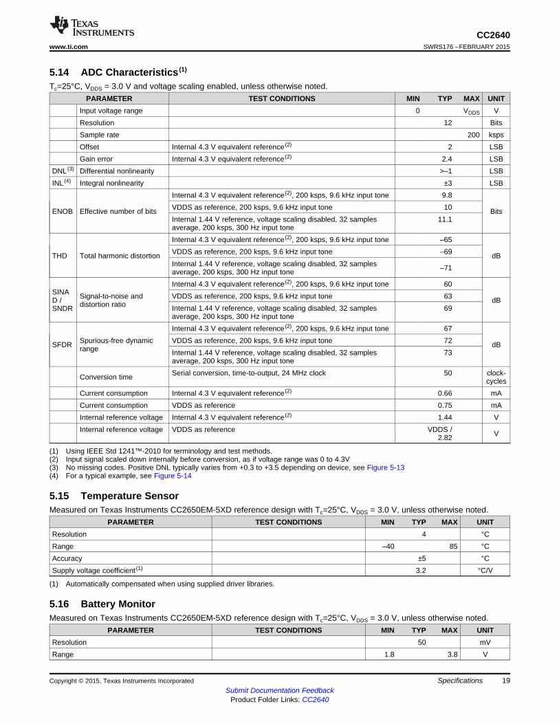
5.14 ADC Characteristics (1)
Tc=25°C, VDDS = 3.0 V and voltage scaling enabled, unless otherwise noted.PARAMETER TEST CONDITIONS MIN TYP MAX UNIT
Input voltage range 0 VDDS VResolution 12 BitsSample rate 200 kspsOffset Internal 4.3 V equivalent reference (2) 2 LSBGain error Internal 4.3 V equivalent reference (2) 2.4 LSB
DNL (3) Differential nonlinearity >–1 LSBINL (4) Integral nonlinearity ±3 LSB
Internal 4.3 V equivalent reference (2), 200 ksps, 9.6 kHz input tone 9.8VDDS as reference, 200 ksps, 9.6 kHz input tone 10ENOB Effective number of bits BitsInternal 1.44 V reference, voltage scaling disabled, 32 samples 11.1average, 200 ksps, 300 Hz input toneInternal 4.3 V equivalent reference (2), 200 ksps, 9.6 kHz input tone –65VDDS as reference, 200 ksps, 9.6 kHz input tone –69THD Total harmonic distortion dBInternal 1.44 V reference, voltage scaling disabled, 32 samples –71average, 200 ksps, 300 Hz input toneInternal 4.3 V equivalent reference (2), 200 ksps, 9.6 kHz input tone 60
SINA Signal-to-noise and VDDS as reference, 200 ksps, 9.6 kHz input tone 63D / dBdistortion ratio Internal 1.44 V reference, voltage scaling disabled, 32 samples 69SNDRaverage, 200 ksps, 300 Hz input toneInternal 4.3 V equivalent reference (2), 200 ksps, 9.6 kHz input tone 67
Spurious-free dynamic VDDS as reference, 200 ksps, 9.6 kHz input tone 72SFDR dBrange Internal 1.44 V reference, voltage scaling disabled, 32 samples 73average, 200 ksps, 300 Hz input toneSerial conversion, time-to-output, 24 MHz clock 50 clock-Conversion time cycles
Current consumption Internal 4.3 V equivalent reference (2) 0.66 mACurrent consumption VDDS as reference 0.75 mAInternal reference voltage Internal 4.3 V equivalent reference (2) 1.44 VInternal reference voltage VDDS as reference VDDS / V2.82
(1) Using IEEE Std 1241™-2010 for terminology and test methods.(2) Input signal scaled down internally before conversion, as if voltage range was 0 to 4.3V(3) No missing codes. Positive DNL typically varies from +0.3 to +3.5 depending on device, see Figure 5-13(4) For a typical example, see Figure 5-14
5.15 Temperature SensorMeasured on Texas Instruments CC2650EM-5XD reference design with Tc=25°C, VDDS = 3.0 V, unless otherwise noted.
PARAMETER TEST CONDITIONS MIN TYP MAX UNITResolution 4 °CRange –40 85 °CAccuracy ±5 °CSupply voltage coefficient (1) 3.2 °C/V
(1) Automatically compensated when using supplied driver libraries.
5.16 Battery MonitorMeasured on Texas Instruments CC2650EM-5XD reference design with Tc=25°C, VDDS = 3.0 V, unless otherwise noted.
PARAMETER TEST CONDITIONS MIN TYP MAX UNITResolution 50 mVRange 1.8 3.8 V
Copyright © 2015, Texas Instruments Incorporated Specifications 19Submit Documentation Feedback
Product Folder Links: CC2640

CC2640SWRS176 –FEBRUARY 2015 www.ti.com
Battery Monitor (continued)Measured on Texas Instruments CC2650EM-5XD reference design with Tc=25°C, VDDS = 3.0 V, unless otherwise noted.
PARAMETER TEST CONDITIONS MIN TYP MAX UNITAccuracy 13 mV
5.17 Continuous Time ComparatorTc=25°C, VDDS = 3.0 V, unless otherwise noted.
PARAMETER TEST CONDITIONS MIN TYP MAX UNITInput voltage range 0 VDDS VExternal reference voltage 0 VDDS VInternal reference voltage DCOUPL as reference 1.27 VOffset 3 mVHysteresis <2 mVDecision time Step from -10mV to +10mV 0.72 µsCurrent consumption when enabled (1) 8.6 µA
(1) Additionally the bias module needs to be enabled when running in standby mode.
5.18 Low-Power Clocked ComparatorTc=25°C, VDDS = 3.0 V, unless otherwise noted.
PARAMETER TEST CONDITIONS MIN TYP MAX UNITInput voltage range 0 VDDS VClock frequency 32 kHzInternal reference voltage, VDDS / 2 1.49 - 1.51 VInternal reference voltage, VDDS / 3 1.01 - 1.03 VInternal reference voltage, VDDS / 4 0.78 - 0.79 VInternal reference voltage, DCOUPL / 1 1.25 - 1.28 VInternal reference voltage, DCOUPL / 2 0.63 - 0.65 VInternal reference voltage, DCOUPL / 3 0.42 - 0.44 VInternal reference voltage, DCOUPL / 4 0.33 - 0.34 VOffset <2 mVHysteresis <5 mVDecision time Step from -50mV to +50mV <1 clock-cycleCurrent consumption when enabled 362 nA
5.19 Programmable Current SourceTc=25°C, VDDS = 3.0 V, unless otherwise noted.
PARAMETER TEST CONDITIONS MIN TYP MAX UNITCurrent source programmable output range 0.25 - µA
20Resolution 0.25 µA
Including current source at maximumCurrent consumption (1) 23 µAprogrammable output
(1) Additionally the bias module needs to be enabled when running in standby mode.
20 Specifications Copyright © 2015, Texas Instruments IncorporatedSubmit Documentation Feedback
Product Folder Links: CC2640

CC2640www.ti.com SWRS176 –FEBRUARY 2015
5.20 DC CharacteristicsPARAMETER TEST CONDITIONS MIN TYP MAX UNIT
TA = 25°C, VDDS = 1.8 VGPIO VOH at 8mA load IOCURR=2, high drive GPIOs only 1.54 VGPIO VOL at 8mA load IOCURR=2, high drive GPIOs only 0.26 VGPIO VOH at 4mA load IOCURR=1 1.58 VGPIO VOL at 4mA load IOCURR=1 0.21 VGPIO pullup current Input mode, pullup enabled, Vpad=0V 71.7 µAGPIO pulldown current Input mode, pulldown enabled, Vpad=VDDS 21.1 µAGPIO high/low input transition, no hysteresis IH=0, transition between reading 0 and reading 1 0.88 VGPIO low-to-high input transition, with hysteresis IH=1, transition voltage for input read as 0→1 1.07 VGPIO high-to-low input transition, with hysteresis IH=1, transition voltage for input read as 1→0 0.74 VGPIO input hysteresis IH=1, difference between 0→1 and 1→0 points 0.33 V
TA = 25°C, VDDS = 3.0 VGPIO VOH at 8mA load IOCURR=2, high drive GPIOs only 2.68 VGPIO VOL at 8mA load IOCURR=2, high drive GPIOs only 0.33 VGPIO VOH at 4mA load IOCURR=1 2.72 VGPIO VOL at 4mA load IOCURR=1 0.28 V
TA = 25°C, VDDS = 3.8 VGPIO pullup current Input mode, pullup enabled, Vpad=0V 277 µAGPIO pulldown current Input mode, pulldown enabled, Vpad=VDDS 113 µAGPIO high/low input transition, no hysteresis IH=0, transition between reading 0 and reading 1 1.67 VGPIO low-to-high input transition, with hysteresis IH=1, transition voltage for input read as 0→1 1.94 VGPIO high-to-low input transition, with hysteresis IH=1, transition voltage for input read as 1→0 1.54 VGPIO input hysteresis IH=1, difference between 0→1 and 1→0 points 0.4 V
5.21 Control Input AC CharacteristicsTA = -40°C to 85°C, VDDS = 1.7 V to 3.8 V, unless otherwise noted.
PARAMETER TEST CONDITIONS MIN TYP MAX UNITRESET_N low duration 1 μs
5.22 Synchronous Serial Interface (SSI) CharacteristicsTc=25°C, VDDS = 3.0 V, unless otherwise noted.
PARAMETER PARAMETER PARAMETER NAME MIN TYP MAX UNITNO.S1 tclk_per SSIClk cycle time 12 65024 system clocks
Copyright © 2015, Texas Instruments Incorporated Specifications 21Submit Documentation Feedback
Product Folder Links: CC2640

VDDS (V)
Out
put p
ower
(dB
m)
1.8 2.3 2.8 3.3 3.80
1
2
3
4
5
6
D003
5XD 5dBm Setting4XS 2dBm Setting
Temperature (qC)
TX
Cur
rent
(m
A)
-40 -30 -20 -10 0 10 20 30 40 50 60 70 800
2
4
6
8
10
12
D002
5XD 5dBm Setting4XS 2dBm Setting
VDDS (V)
TX
Cur
rent
(m
A)
1.8 2 2.2 2.4 2.6 2.8 3 3.2 3.4 3.6 3.84
5
6
7
8
9
10
11
12
13
14
15
16
D015
4XS 2-dBm Setting5XD 5-dBm Setting
Temperature (qC)
RX
Cur
rent
(m
A)
-40 -30 -20 -10 0 10 20 30 40 50 60 70 805.6
5.8
6
6.2
6.4
6.6
6.8
7
D001
5XD RX Current4XS RX Current
Temperature (qC)
Sen
sitiv
ity (
dBm
)
-40 -30 -20 -10 0 10 20 30 40 50 60 70 80-99
-98
-97
-96
-95
-94
Sensitivity 4XSSensitivity 5XD
Temperature (qC)
Out
put P
ower
(dB
m)
-40 -30 -20 -10 0 10 20 30 40 50 60 70 800
1
2
3
4
5
6
4XS 2-dBm Setting5XD 5-dBm Setting
CC2640SWRS176 –FEBRUARY 2015 www.ti.com
5.23 Typical Characteristics
Figure 5-2. Output Power vs TemperatureFigure 5-1. BLE Sensitivity vs Temperature
Figure 5-3. Transmit Current Consumption vs. Supply VoltageFigure 5-4. RX Mode Current Consumption vs Temperature(VDDS)
Figure 5-6. TX Output Power vs Supply Voltage (VDDS)Figure 5-5. TX Mode Current Consumption vs Temperature
22 Specifications Copyright © 2015, Texas Instruments IncorporatedSubmit Documentation Feedback
Product Folder Links: CC2640

Input Frequency (Hz)
Effe
ctiv
e N
umbe
r of
Bits
200300 500 1000 2000 5000 10000 20000 1000009.4
9.6
9.8
10
10.2
10.4
10.6
10.8
11
11.2
11.4
D009
Fs= 200 kHz, No AveragingFs= 200 kHz, 32 samples averaging
VDDS (V)
AD
C C
ode
1.8 2.3 2.8 3.3 3.81004.8
1005
1005.2
1005.4
1005.6
1005.8
1006
1006.2
1006.4
D012
VDDS (V)
Cur
rent
Con
sum
ptio
n (m
A)
1.8 2.3 2.8 3.3 3.82
2.5
3
3.5
4
4.5
5
D007
Active Mode Current
Temperature (qC)
Cur
rent
(uA
)
-20 -10 0 10 20 30 40 50 60 70 800
0.5
1
1.5
2
2.5
3
3.5
4
D008
Standby Mode Current
VDDS (V)
Sen
sitiv
ity (
dBm
)
1.8 2.3 2.8 3.3 3.8-101
-100
-99
-98
-97
-96
-95
D004
BLE 5XD SensitivityBLE 4XS Sensitivity
Temperature (qC)
Act
ive
Mod
e C
urre
nt C
onsu
mps
tion
(mA
)
-40 -30 -20 -10 0 10 20 30 40 50 60 70 802.85
2.9
2.95
3
3.05
3.1
D006
Active Mode Current
CC2640www.ti.com SWRS176 –FEBRUARY 2015
Figure 5-7. BLE Sensitivity vs Supply Voltage (VDDS)Figure 5-8. Active Mode Current Consumption vs Temperature
Figure 5-9. Active Mode Current Consumption vs Supply Figure 5-10. Standby Mode Current Consumption With RCOSCVoltage (VDDS) RTC vs Temperature
Figure 5-11. Effective number of bits vs Input frequency Figure 5-12. SoC ADC Output vs Supply Voltage (Fixed Input,(Internal Reference, No Scaling) Internal Reference, No Scaling)
Copyright © 2015, Texas Instruments Incorporated Specifications 23Submit Documentation Feedback
Product Folder Links: CC2640

Input Frequency (Hz)
Effe
ctiv
e N
umbe
r of
Bits
200300 500 1000 2000 5000 10000 20000 1000009.4
9.6
9.8
10
10.2
10.4
10.6
10.8
11
11.2
11.4
D009
Fs= 200 kHz, No AveragingFs= 200 kHz, 32 samples averaging
Temperature (qC)
AD
C C
ode
-40 -30 -20 -10 0 10 20 30 40 50 60 70 801004.5
1005
1005.5
1006
1006.5
1007
1007.5
D013
ADC Code
INL
0 200 400 600 800 1000 1200 1400 1600 1800 2000 2200 2400 2600 2800 3000 3200 3400 3600 3800 4000 4200-4
-3
-2
-1
0
1
2
3
D011
ADC Code
DN
L
0
200
400
600
800
1000
1200
1400
1600
1800
2000
2200
2400
2600
2800
3000
3200
3400
3600
3800
4000
4200
-1.5
-1
-0.5
0
0.5
1
1.5
2
2.5
3
3.5
D010
CC2640SWRS176 –FEBRUARY 2015 www.ti.com
Figure 5-13. DNL vs. ADC Code (Internal Reference, No Scaling)
Figure 5-14. INL vs. ADC Code (Internal Reference, No Scaling)
Figure 5-15. SoC ADC Output vs Temperature (Fixed Input, Figure 5-16. ENOB vs Sampling FrequencyInternal Reference, No Scaling) (Input frequency = Fs/10)
24 Specifications Copyright © 2015, Texas Instruments IncorporatedSubmit Documentation Feedback
Product Folder Links: CC2640

CC2640www.ti.com SWRS176 –FEBRUARY 2015
6 Detailed Description
6.1 OverviewSection 1.4 shows a block diagram of the core modules of the CC26xx product family.
6.2 Main CPUThe SimpleLink CC2640 Wireless MCU contains an ARM Cortex-M3 (CM3) 32-bit CPU, which runs theapplication and the higher layers of the protocol stack.
The CM3 processor provides a high-performance, low-cost platform that meets the system requirementsof minimal memory implementation, and low-power consumption, while delivering outstandingcomputational performance and exceptional system response to interrupts.
CM3 features include:• 32-bit ARM Cortex-M3 architecture optimized for small-footprint embedded applications• Outstanding processing performance combined with fast interrupt handling• ARM Thumb®-2 mixed 16- and 32 bit instruction set delivers the high performance expected of a 32 bit
ARM core in a compact memory size usually associated with 8- and 16-bit devices, typically in therange of a few kilobytes of memory for microcontroller-class applications:– Single-cycle multiply instruction and hardware divide– Atomic bit manipulation (bit-banding), delivering maximum memory use and streamlined peripheral
control– Unaligned data access, enabling data to be efficiently packed into memory
• Fast code execution permits slower processor clock or increases sleep mode time• Harvard architecture characterized by separate buses for instruction and data• Efficient processor core, system, and memories• Hardware division and fast digital-signal-processing oriented multiply accumulate• Saturating arithmetic for signal processing• Deterministic, high-performance interrupt handling for time-critical applications• Enhanced system debug with extensive breakpoint and trace capabilities• Serial wire trace reduces the number of pins required for debugging and tracing• Migration from the ARM7™ processor family for better performance and power efficiency• Optimized for single-cycle flash memory use• Ultra-low power consumption with integrated sleep modes• 1.25 DMIPS per MHz
6.3 RF CoreThe RF Core contains an ARM Cortex M0 that interfaces the analog RF and base-band circuitries,handles data to and from the system side, and assembles the information bits in a given packet structure.The RF core offers a high level, command-based API to the main CPU.
The RF core is capable of autonomously handling the time-critical aspects of the radio protocols(Bluetooth Low Energy) thus offloading the main CPU and leaving more resources for the user application.
The RF core has a dedicated 4-KB SRAM block and runs initially from separate ROM memory. The ARMCortex M0 is not programmable by customers.
Copyright © 2015, Texas Instruments Incorporated Detailed Description 25Submit Documentation Feedback
Product Folder Links: CC2640
CC2640SWRS176 –FEBRUARY 2015 www.ti.com
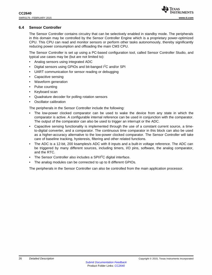
6.4 Sensor ControllerThe Sensor Controller contains circuitry that can be selectively enabled in standby mode. The peripheralsin this domain may be controlled by the Sensor Controller Engine which is a proprietary power-optimizedCPU. This CPU can read and monitor sensors or perform other tasks autonomously, thereby significantlyreducing power consumption and offloading the main CM3 CPU.
The Sensor Controller is set up using a PC-based configuration tool, called Sensor Controller Studio, andtypical use cases may be (but are not limited to):• Analog sensors using integrated ADC• Digital sensors using GPIOs and bit-banged I2C and/or SPI• UART communication for sensor reading or debugging• Capacitive sensing• Waveform generation• Pulse counting• Keyboard scan• Quadrature decoder for polling rotation sensors• Oscillator calibration
The peripherals in the Sensor Controller include the following:• The low-power clocked comparator can be used to wake the device from any state in which the
comparator is active. A configurable internal reference can be used in conjunction with the comparator.The output of the comparator can also be used to trigger an interrupt or the ADC.
• Capacitive sensing functionality is implemented through the use of a constant current source, a time-to-digital converter, and a comparator. The continuous time comparator in this block can also be usedas a higher-accuracy alternative to the low-power clocked comparator. The Sensor Controller will takecare of baseline tracking, hysteresis, filtering and other related functions.
• The ADC is a 12-bit, 200 ksamples/s ADC with 8 inputs and a built-in voltage reference. The ADC canbe triggered by many different sources, including timers, I/O pins, software, the analog comparator,and the RTC.
• The Sensor Controller also includes a SPI/I2C digital interface.• The analog modules can be connected to up to 8 different GPIOs.
The peripherals in the Sensor Controller can also be controlled from the main application processor.
26 Detailed Description Copyright © 2015, Texas Instruments IncorporatedSubmit Documentation Feedback
Product Folder Links: CC2640

CC2640www.ti.com SWRS176 –FEBRUARY 2015
Table 6-1. GPIOs Connected to the Sensor Controller (1)
Analog capable 7x7 RGZ DIO# 5x5 RHB DIO# 4x4 RSM DIO#Y 30 14Y 29 13Y 28 12Y 27 11 9Y 26 9 8Y 25 10 7Y 24 8 6Y 23 7 5N 7 4 2N 6 3 1N 5 2 0N 4 1N 3 0N 2N 1N 0
(1) Depending on the package size, up to 16 pins can be connected to the Sensor Controller. Up to 8 ofthem can be connected to analog modules
6.5 MemoryThe flash memory provides nonvolatile storage for code and data. The flash memory is in-systemprogrammable.
The SRAM (static RAM) can be used for both storage of data and execution of code and is split into two4-KB blocks and two 6-KB blocks. Retention of the RAM contents in standby mode can be enabled ordisabled individually for each block to minimize power consumption. In addition, if flash cache is disabled,the 8-KB cache can be used as a general-purpose RAM.
The ROM provides preprogrammed embedded TI RTOS kernel, Driverlib and lower layer protocol stacksoftware (Bluetooth Low Energy Controller). It also contains a bootloader that can be used to reprogramthe device using SPI or UART.
6.6 DebugThe on-chip debug support is done through a dedicated cJTAG (IEEE 1149.7) or JTAG (IEEE 1149.1)interface.
Copyright © 2015, Texas Instruments Incorporated Detailed Description 27Submit Documentation Feedback
Product Folder Links: CC2640

CC2640SWRS176 –FEBRUARY 2015 www.ti.com
6.7 Power ManagementTo minimize power consumption, the CC2640 supports a number of power modes and powermanagement features (see Table 6-2).
Table 6-2. Power Modes
Software Configurable Power ModesMode Reset Pin Held
Active Idle Standby ShutdownCPU Active Off Off Off OffFlash On Available Off Off OffSRAM On On On Off OffRadio Available Available Off Off OffSupply System On On Duty Cycled Off OffCurrent 1.45 mA + 31 µA/MHz 550 µA 1 µA 0.15 µA 0.1 µAWake-up Time to CPU Active (1) – 14 µs 151 µs 1015 µs 1015 µsRegister Retention Full Full Partial No NoSRAM Retention Full Full Full No No
XOSC_HF or XOSC_HF orHigh-Speed Clock Off Off OffRCOSC_HF RCOSC_HFXOSC_LF or XOSC_LF or XOSC_LF orLow-Speed Clock Off OffRCOSC_LF RCOSC_LF RCOSC_LF
Peripherals Available Available Off Off OffSensor Controller Available Available Available Off OffWake-up on RTC Available Available Available Off OffWake-up on Pin Edge Available Available Available Available OffWake-up on Reset Pin Available Available Available Available Available
(1) Not including RTOS overhead
In Active mode, the application CM3 CPU is actively executing code. Active mode provides normaloperation of the processor and all of the peripherals that are currently enabled. The system clock can beany available clock source (see Table 6-2).
In Idle mode, all active peripherals can be clocked, but the Application CPU core and memory are notclocked and no code is executed. Any interrupt event will bring the processor back into Active mode.
In Standby, only the AON (Always-on) domain is active. An external wake event, RTC event, or SensorController event is required to bring the device back to Active. MCU peripherals with retention do not needto be reconfigured when waking up again and the CPU will continue execution from where it went intoStandby. All GPIOs are latched in Standby.
In Shutdown, the device is entirely turned off, including the AON domain and Sensor Controller, I/Os arelatched with the value they had before entering Shutdown. A change of state on any I/O pin defined as a"wake from Shutdown pin" will wake up the device and function as a reset trigger. The CPU candifferentiate between reset in this way and reset-by-reset pin or power-on-reset by reading the reset statusregister. The only state retained in this mode is the latched I/O state and the Flash memory contents.
The Sensor Controller is an autonomous processor that can control the peripherals in the SensorController independently of the main CPU. This means that the main CPU does not have to wake up to forexample execute an ADC sample or poll a digital sensor over SPI, and saves both current and wake-uptime that would otherwise be wasted. The Sensor Controller Studio enables the user to configure theSensor Controller and choose which peripherals are controlled and which conditions will wake up the mainCPU.
28 Detailed Description Copyright © 2015, Texas Instruments IncorporatedSubmit Documentation Feedback
Product Folder Links: CC2640

CC2640www.ti.com SWRS176 –FEBRUARY 2015
6.8 Clock SystemsThe CC2640 supports two external and two internal clock sources.
A 24 MHz crystal is required as the frequency reference for the radio. This signal is doubled internally tocreate a 48 MHz clock.
The 32 kHz crystal is optional. Bluetooth low energy requires a slow-speed clock with better than ±500ppm accuracy if the device is to enter any sleep mode while maintaining a connection. The internal 32 kHzRC oscillator can in some use cases be compensated to meet the requirements. The low-speed crystaloscillator is designed for use with a 32 kHz watch-type crystal.
The internal high-speed oscillator (48 MHz) can be used as a clock source for the CPU subsystem.
The internal low-speed oscillator (32.768 kHz) can be used as a reference if the low-power crystaloscillator is not used.
The 32 kHz clock source can be used as external clocking reference through GPIO.
6.9 General Peripherals and ModulesThe I/O controller controls the digital I/O pins and contains multiplexer circuitry to allow a set of peripheralsto be assigned to I/O pins in a flexible manner. All digital I/Os are interrupt and wake-up capable, have aprogrammable pullup and pulldown function and can generate an interrupt on a negative or positive edge(configurable). When configured as an output, pins can function as either push-pull or open-drain. FiveGPIOs have high drive capabilities (marked in bold in Section 4).
The SSIs are synchronous serial interfaces that are compatible with SPI, MICROWIRE, and TexasInstruments synchronous serial interfaces. The SSIs support both SPI master and slave up to 4 MHz.
The UART implements a universal asynchronous receiver/transmitter function. It supports flexible baud-rate generation up to a maximum of 3 Mbps and is compatible with the Bluetooth HCI specifications.
Timer 0 is a general-purpose timer module (GPTM), which provides two 16-bit timers. The GPTM can beconfigured to operate as a single 32-bit timer, dual 16-bit timers or as a PWM module.
Timer 1, Timer 2, and Timer 3 are also GPTMs. Each of these timers is functionally equivalent to Timer 0.
In addition to these four timers, the RF core has its own timer to handle timing for RF protocols; the RFtimer can be synchronized to the RTC.
The I2C interface is used to communicate with devices compatible with the I2C standard. The I2C interfaceis capable of 100 kHz and 400 kHz operation, and can serve as both I2C master and I2C slave.
The TRNG module provides a true, nondeterministic noise source for the purpose of generating keys,initialization vectors (IVs), and other random number requirements. The TRNG is built on 24 ringoscillators that create unpredictable output to feed a complex nonlinear combinatorial circuit.
The watchdog timer is used to regain control if the system fails due to a software error after an externaldevice fails to respond as expected. The watchdog timer can generate an interrupt or a reset when apredefined time-out value is reached.
The device includes a direct memory access (µDMA) controller. The µDMA controller provides a way tooffload data transfer tasks from the CM3 CPU, allowing for more efficient use of the processor and theavailable bus bandwidth. The µDMA controller can perform transfer between memory and peripherals. TheµDMA controller has dedicated channels for each supported on-chip module and can be programmed toautomatically perform transfers between peripherals and memory as the peripheral is ready to transfermore data. Some features of the µDMA controller include the following (this is not an exhaustive list):• Highly flexible and configurable channel operation of up to 32 channels• Transfer modes: Memory-to-memory, memory-to-peripheral, peripheral-to-memory, and peripheral-to-
peripheral• Data sizes of 8, 16, and 32 bits
Copyright © 2015, Texas Instruments Incorporated Detailed Description 29Submit Documentation Feedback
Product Folder Links: CC2640

CC2640SWRS176 –FEBRUARY 2015 www.ti.com
The AON domain contains circuitry that is always enabled, except for in Shutdown (where the digitalsupply is off). This circuitry includes the following:• The RTC can be used to wake the device from any state where it is active. The RTC contains three
compare and one capture registers. With software support, the RTC can be used for clock andcalendar operation. The RTC is clocked from the 32 kHz RC oscillator or crystal. The RTC can also becompensated to tick at the correct frequency even when the internal 32 kHz RC oscillator is usedinstead of a crystal.
• The battery monitor and temperature sensor are accessible by software and give a battery statusindication as well as a coarse temperature measure.
6.10 System ArchitectureDepending on the product configuration, CC26xx can function either as a Wireless Network Processor(WNP – an IC running the wireless protocol stack, with the application running on a separate MCU), or asa System-on-Chip (SoC), with the application and protocol stack running on the ARM CM3 core inside thedevice.
In the first case, the external host MCU communicates with the device using SPI or UART. In the secondcase, the application must be written according to the application framework supplied with the wirelessprotocol stack.
30 Detailed Description Copyright © 2015, Texas Instruments IncorporatedSubmit Documentation Feedback
Product Folder Links: CC2640
Antenna(50 Ohm)
1 pF
1 pF2.4 nH
2.4-2.7 nH
6.8 pF
6.2-6.8 nH
Antenna(50 Ohm)
1.2 pF
15 nH2 nH
1.2 pF
Antenna(50 Ohm)
1.2 pF
2 nH
1.2 pF
Antenna(50 Ohm)
1.2 pF
2 nH
1.2 pF
Pin 1 (RF P)
Pin 2 (RF N)
Pin 3 (RXTX)
Pin 1 (RF P)
Pin 2 (RF N)
Pin 1 (RF P)
Pin 2 (RF N)
Red = Not necessary if internal bias is used
Red = Not necessary if internal bias is used
Differential operation
Single ended operation
Single ended operation with 2 antennas
Pin 3 (RXTX)
15 nH
15 nH
CC 26 xx
( GND exposed die
attached pad )
Pin 3/4 (RXTX)
Pin 1 (RF P)
Pin 2 (RF N)
24MHz XTAL
(Load caps on chip)
10uF
10uH
Optional inductor.
Only needed for
DCDC operation
12 pF
12 pF
12 pF
12 pF
2 nH 2 nH
1 pF
input decoupling10uF ± 22uF
To VDDR pins
VDDS_DCDC
DCDC_SW
Red = Not necessary if internal bias is used
CC2640www.ti.com SWRS176 –FEBRUARY 2015
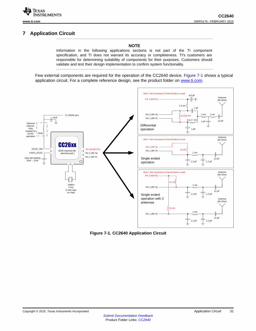
7 Application Circuit
NOTEInformation in the following applications sections is not part of the TI componentspecification, and TI does not warrant its accuracy or completeness. TI's customers areresponsible for determining suitability of components for their purposes. Customers shouldvalidate and test their design implementation to confirm system functionality.
Few external components are required for the operation of the CC2640 device. Figure 7-1 shows a typicalapplication circuit. For a complete reference design, see the product folder on www.ti.com.
Figure 7-1. CC2640 Application Circuit
Copyright © 2015, Texas Instruments Incorporated Application Circuit 31Submit Documentation Feedback
Product Folder Links: CC2640

CC 26 xx
( GND exposed die
attached pad )
Pin 3/4 (RXTX)
Pin 1 (RF P)
Pin 2 (RF N)
24MHz XTAL
(Load caps on chip)
10uF
10uH
VDDS_DCDC input decoupling
10uF ± 22uF
To all VDDR Pins
VDDS_DCDC Pin
DCDC_SW PinCC 26 xx
( GND exposed die
attached pad )
Pin 3/4 (RXTX)
Pin 1 (RF P)
Pin 2 (RF N)
24MHz XTAL
(Load caps on chip)
2.2uF
1.7V ± 1.95V to all VDDR- and VDDS Pins except VDDS_DCDC
VDDS_DCDC Pin
DCDC_SW Pin
Ext regulator
1.8V ± 3.8V to all VDDS Pins
Internal DCDC regulator External regulator
CC 26 xx
( GND exposed die
attached pad )
Pin 3/4 (RXTX)
Pin 1 (RF P)
Pin 2 (RF N)
24MHz XTAL
(Load caps on chip)
VDDS_DCDC input decoupling
10uF ± 22uF
To all VDDR Pins
VDDS_DCDC Pin
DCDC_SW Pin
1.8V ± 3.8V Supply voltage
10uF
NC
To all VDDS Pins
Internal LDO regulator
CC2640SWRS176 –FEBRUARY 2015 www.ti.com
Figure 7-2. Supply Voltage Configurations
Power supply decoupling capacitors are not shown. Digital I/Os not included. Pin positions, andcomponent values are not final. For detailed overview of power supply decoupling and wiring, see the TIreference designs and the CC26xx technical reference manual (Section 8.2).
Figure 7-1 shows that the RF front end can be used both differentially and single-endedly with the optionof having internal or external biasing. These options allow for various trade-offs between cost, board-space, and RF performance. Differential operation with external bias gives the best performance whilesingle-ended operation with internal bias gives the least amount of external components and the lowestpower consumption.
32 Application Circuit Copyright © 2015, Texas Instruments IncorporatedSubmit Documentation Feedback
Product Folder Links: CC2640

CC2640www.ti.com SWRS176 –FEBRUARY 2015
8 Device and Documentation Support
8.1 Device Support
8.1.1 Development SupportTI offers an extensive line of development tools, including tools to evaluate the performance of theprocessors, generate code, develop algorithm implementations, and fully integrate and debug softwareand hardware modules.
The following products support development of the CC2640 device applications:
Software Tools:
SmartRF™ Studio 7:
SmartRF Studio is a PC application that helps designers of radio systems to easily evaluate the RF-IC atan early stage in the design process.• Test functions for sending and receiving radio packets, continuous wave transmit and receive• Evaluate RF performance on custom boards by wiring it to a supported evaluation board or debugger• Can also be used without any hardware, but then only to generate, edit and export radio configuration
settings• Can be used in combination with several development kits for Texas Instruments’ CCxxxx RF-ICs
Sensor Controller Studio:
Sensor Controller Studio provides a development environment for the CC26xx Sensor Controller. TheSensor Controller is a proprietary, power-optimized CPU in the CC26xx, which can perform simplebackground tasks autonomously and independent of the System CPU state.• Allows for Sensor Controller task algorithms to be implemented using a C-like programming language• Outputs a Sensor Controller Interface driver, which incorporates the generated Sensor Controller
machine code and associated definitions• Allows for rapid development by using the integrated Sensor Controller task testing and debugging
functionality. This allows for live visualization of sensor data and algorithm verification.
IDEs and Compilers:
Code Composer Studio:• Integrated development environment with project management tools and editor• Code Composer Studio (CCS) 6.1 and later has built-in support for the CC26xx device family• Best support for XDS debuggers; XDS100v3, XDS110 and XDS200• High integration with TI-RTOS with support for TI-RTOS Object View
IAR Embedded Workbench for ARM• Integrated development environment with project management tools and editor• IAR EWARM 7.30.3 and later has built-in support for the CC26xx device family• Broad debugger support, supporting XDS100v3, XDS200, IAR I-Jet and Segger J-Link• Integrated development environment with project management tools and editor• RTOS plugin available for TI-RTOS
For a complete listing of development-support tools for the CC2640 platform, visit the Texas Instrumentswebsite at www.ti.com. For information on pricing and availability, contact the nearest TI field sales officeor authorized distributor.
Copyright © 2015, Texas Instruments Incorporated Device and Documentation Support 33Submit Documentation Feedback
Product Folder Links: CC2640

CC2640SWRS176 –FEBRUARY 2015 www.ti.com
8.1.2 Device NomenclatureTo designate the stages in the product development cycle, TI assigns prefixes to all part numbers and/ordate-code. Each device has one of three prefixes/identifications: X, P, or null (no prefix) (for example,CC2640 is in production; therefore, no prefix/identification is assigned).
Device development evolutionary flow:
X Experimental device that is not necessarily representative of the final device's electricalspecifications and may not use production assembly flow.
P Prototype device that is not necessarily the final silicon die and may not necessarily meetfinal electrical specifications.
null Production version of the silicon die that is fully qualified.
Production devices have been characterized fully, and the quality and reliability of the device have beendemonstrated fully. TI's standard warranty applies.
Predictions show that prototype devices (X or P) have a greater failure rate than the standard productiondevices. Texas Instruments recommends that these devices not be used in any production systembecause their expected end-use failure rate still is undefined. Only qualified production devices are to beused.
TI device nomenclature also includes a suffix with the device family name. This suffix indicates thepackage type (for example, RSM).
For orderable part numbers of CC2640 devices in the RSM, RHB or RGZ package types, see thePackage Option Addendum of this document, the TI website (www.ti.com), or contact your TI salesrepresentative.
34 Device and Documentation Support Copyright © 2015, Texas Instruments IncorporatedSubmit Documentation Feedback
Product Folder Links: CC2640

CC2640www.ti.com SWRS176 –FEBRUARY 2015
8.2 Documentation SupportThe following documents describe the CC2640. Copies of these documents are available on the Internetat www.ti.com.
SWCU117 Technical Reference Manual. Texas Instruments CC26xx Family of Products
SWRS058 Silicon Errata. Texas Instruments CC26xx™ Family of Products
8.2.1 Community ResourcesThe following links connect to TI community resources. Linked contents are provided "AS IS" by therespective contributors. They do not constitute TI specifications and do not necessarily reflect TI's views;see TI's Terms of Use.
TI E2E™ Online Community TI's Engineer-to-Engineer (E2E) Community. Created to fostercollaboration among engineers. At e2e.ti.com, you can ask questions, share knowledge,explore ideas and help solve problems with fellow engineers.
TI Embedded Processors Wiki Texas Instruments Embedded Processors Wiki. Established to helpdevelopers get started with Embedded Processors from Texas Instruments and to fosterinnovation and growth of general knowledge about the hardware and software surroundingthese devices.
8.3 Additional InformationTexas Instruments offers a wide selection of cost-effective, low-power RF solutions for proprietary andstandard-based wireless applications for use in industrial and consumer applications. The selectionincludes RF transceivers, RF transmitters, RF front ends, and Systems-on-Chips as well as varioussoftware solutions for the sub-1-GHz and 2.4-GHz frequency bands.
In addition, Texas Instruments provides a large selection of support collateral such as development tools,technical documentation, reference designs, application expertise, customer support, third-party anduniversity programs.
The Low-Power RF E2E Online Community provides technical support forums, videos and blogs, and thechance to interact with engineers from all over the world.
With a broad selection of product solutions, end-application possibilities, and a range of technical support,Texas Instruments offers the broadest low-power RF portfolio.
8.3.1 Texas Instruments Low-Power RF WebsiteTexas Instruments' Low-Power RF website has all the latest products, application and design notes, FAQsection, news and events updates. Go to www.ti.com/lprf.
8.3.2 Low-Power RF Online Community• Forums, videos, and blogs• RF design help• E2E interaction
Join at: www.ti.com/lprf-forum.
Copyright © 2015, Texas Instruments Incorporated Device and Documentation Support 35Submit Documentation Feedback
Product Folder Links: CC2640

CC2640SWRS176 –FEBRUARY 2015 www.ti.com
8.3.3 Texas Instruments Low-Power RF Developer NetworkTexas Instruments has launched an extensive network of low-power RF development partners to helpcustomers speed up their application development. The network consists of recommended companies, RFconsultants, and independent design houses that provide a series of hardware module products anddesign services, including:• RF circuit, low-power RF, and ZigBee design services• Low-power RF and ZigBee module solutions and development tools• RF certification services and RF circuit manufacturing
For help with modules, engineering services or development tools:
Search the Low-Power RF Developer Network to find a suitable partner. www.ti.com/lprfnetwork
8.3.4 Low-Power RF eNewsletterThe Low-Power RF eNewsletter is up-to-date on new products, news releases, developers’ news, andother news and events associated with low-power RF products from TI. The Low-Power RF eNewsletterarticles include links to get more online information.
Sign up at: www.ti.com/lprfnewsletter
8.4 TrademarksIAR Embedded Workbench is a registered trademark of IAR Systems AB.SimpleLink, SmartRF, Code Composer Studio, CC26xx, E2E are trademarks of Texas Instruments.ARM7 is a trademark of ARM Limited.ARM, Cortex are registered trademarks of ARM Limited (or its subsidiaries).ARM Thumb is a registered trademark of ARM Limited.Bluetooth is a registered trademark of Bluetooth SIG, Inc.CoreMark is a registered trademark of Embedded Microprocessor Benchmark Consortium.IEEE Std 1241 is a trademark of Institute of Electrical and Electronics Engineers, Incorporated.ZigBee is a registered trademark of ZigBee Alliance, Inc.
8.5 Electrostatic Discharge CautionThis integrated circuit can be damaged by ESD. Texas Instruments recommends that all integrated circuits be handled withappropriate precautions. Failure to observe proper handling and installation procedures can cause damage.
ESD damage can range from subtle performance degradation to complete device failure. Precision integrated circuits may be moresusceptible to damage because very small parametric changes could cause the device not to meet its published specifications.
8.6 Export Control NoticeRecipient agrees to not knowingly export or re-export, directly or indirectly, any product or technical data(as defined by the U.S., EU, and other Export Administration Regulations) including software, or anycontrolled product restricted by other applicable national regulations, received from Disclosing party underthis Agreement, or any direct product of such technology, to any destination to which such export or re-export is restricted or prohibited by U.S. or other applicable laws, without obtaining prior authorization fromU.S. Department of Commerce and other competent Government authorities to the extent required bythose laws.
8.7 GlossarySLYZ022 — TI Glossary.
This glossary lists and explains terms, acronyms and definitions.
36 Device and Documentation Support Copyright © 2015, Texas Instruments IncorporatedSubmit Documentation Feedback
Product Folder Links: CC2640

CC2640www.ti.com SWRS176 –FEBRUARY 2015
9 Mechanical Packaging and Orderable Information
9.1 Packaging InformationThe following pages include mechanical packaging and orderable information. This information is the mostcurrent data available for the designated devices. This data is subject to change without notice andrevision of this document. For browser-based versions of this data sheet, refer to the left-hand navigation.
Copyright © 2015, Texas Instruments Incorporated Mechanical Packaging and Orderable Information 37Submit Documentation Feedback
Product Folder Links: CC2640

PACKAGE OPTION ADDENDUM
www.ti.com 5-Sep-2015
Addendum-Page 1
PACKAGING INFORMATION
Orderable Device Status(1)
Package Type PackageDrawing
Pins PackageQty
Eco Plan(2)
Lead/Ball Finish(6)
MSL Peak Temp(3)
Op Temp (°C) Device Marking(4/5)
Samples
CC2640F128RGZR ACTIVE VQFN RGZ 48 2500 Green (RoHS& no Sb/Br)
CU NIPDAU Level-3-260C-168 HR -40 to 85 CC2640F128
CC2640F128RGZT ACTIVE VQFN RGZ 48 250 Green (RoHS& no Sb/Br)
CU NIPDAU Level-3-260C-168 HR -40 to 85 CC2640F128
CC2640F128RHBR ACTIVE VQFN RHB 32 3000 Green (RoHS& no Sb/Br)
CU NIPDAU | Call TI Level-3-260C-168 HR -40 to 85 CC2640F128
CC2640F128RHBT ACTIVE VQFN RHB 32 250 Green (RoHS& no Sb/Br)
CU NIPDAU | Call TI Level-3-260C-168 HR -40 to 85 CC2640F128
CC2640F128RSMR ACTIVE VQFN RSM 32 3000 Green (RoHS& no Sb/Br)
CU NIPDAU Level-3-260C-168 HR -40 to 85 CC2640F128
CC2640F128RSMT ACTIVE VQFN RSM 32 250 Green (RoHS& no Sb/Br)
CU NIPDAU Level-3-260C-168 HR -40 to 85 CC2640F128
(1) The marketing status values are defined as follows:ACTIVE: Product device recommended for new designs.LIFEBUY: TI has announced that the device will be discontinued, and a lifetime-buy period is in effect.NRND: Not recommended for new designs. Device is in production to support existing customers, but TI does not recommend using this part in a new design.PREVIEW: Device has been announced but is not in production. Samples may or may not be available.OBSOLETE: TI has discontinued the production of the device.
(2) Eco Plan - The planned eco-friendly classification: Pb-Free (RoHS), Pb-Free (RoHS Exempt), or Green (RoHS & no Sb/Br) - please check http://www.ti.com/productcontent for the latest availabilityinformation and additional product content details.TBD: The Pb-Free/Green conversion plan has not been defined.Pb-Free (RoHS): TI's terms "Lead-Free" or "Pb-Free" mean semiconductor products that are compatible with the current RoHS requirements for all 6 substances, including the requirement thatlead not exceed 0.1% by weight in homogeneous materials. Where designed to be soldered at high temperatures, TI Pb-Free products are suitable for use in specified lead-free processes.Pb-Free (RoHS Exempt): This component has a RoHS exemption for either 1) lead-based flip-chip solder bumps used between the die and package, or 2) lead-based die adhesive used betweenthe die and leadframe. The component is otherwise considered Pb-Free (RoHS compatible) as defined above.Green (RoHS & no Sb/Br): TI defines "Green" to mean Pb-Free (RoHS compatible), and free of Bromine (Br) and Antimony (Sb) based flame retardants (Br or Sb do not exceed 0.1% by weightin homogeneous material)
(3) MSL, Peak Temp. - The Moisture Sensitivity Level rating according to the JEDEC industry standard classifications, and peak solder temperature.
(4) There may be additional marking, which relates to the logo, the lot trace code information, or the environmental category on the device.
(5) Multiple Device Markings will be inside parentheses. Only one Device Marking contained in parentheses and separated by a "~" will appear on a device. If a line is indented then it is a continuationof the previous line and the two combined represent the entire Device Marking for that device.

PACKAGE OPTION ADDENDUM
www.ti.com 5-Sep-2015
Addendum-Page 2
(6) Lead/Ball Finish - Orderable Devices may have multiple material finish options. Finish options are separated by a vertical ruled line. Lead/Ball Finish values may wrap to two lines if the finishvalue exceeds the maximum column width.
Important Information and Disclaimer:The information provided on this page represents TI's knowledge and belief as of the date that it is provided. TI bases its knowledge and belief on informationprovided by third parties, and makes no representation or warranty as to the accuracy of such information. Efforts are underway to better integrate information from third parties. TI has taken andcontinues to take reasonable steps to provide representative and accurate information but may not have conducted destructive testing or chemical analysis on incoming materials and chemicals.TI and TI suppliers consider certain information to be proprietary, and thus CAS numbers and other limited information may not be available for release.
In no event shall TI's liability arising out of such information exceed the total purchase price of the TI part(s) at issue in this document sold by TI to Customer on an annual basis.

TAPE AND REEL INFORMATION
*All dimensions are nominal
Device PackageType
PackageDrawing
Pins SPQ ReelDiameter
(mm)
ReelWidth
W1 (mm)
A0(mm)
B0(mm)
K0(mm)
P1(mm)
W(mm)
Pin1Quadrant
CC2640F128RGZR VQFN RGZ 48 2500 330.0 16.4 7.3 7.3 1.1 12.0 16.0 Q2
CC2640F128RGZT VQFN RGZ 48 250 180.0 16.4 7.3 7.3 1.1 12.0 16.0 Q2
CC2640F128RHBR VQFN RHB 32 3000 330.0 12.4 5.3 5.3 1.1 8.0 12.0 Q2
CC2640F128RHBT VQFN RHB 32 250 180.0 12.4 5.3 5.3 1.1 8.0 12.0 Q2
CC2640F128RSMR VQFN RSM 32 3000 330.0 12.4 4.25 4.25 1.15 8.0 12.0 Q2
CC2640F128RSMT VQFN RSM 32 250 180.0 12.4 4.25 4.25 1.15 8.0 12.0 Q2
PACKAGE MATERIALS INFORMATION
www.ti.com 3-Aug-2015
Pack Materials-Page 1

*All dimensions are nominal
Device Package Type Package Drawing Pins SPQ Length (mm) Width (mm) Height (mm)
CC2640F128RGZR VQFN RGZ 48 2500 367.0 367.0 38.0
CC2640F128RGZT VQFN RGZ 48 250 210.0 185.0 35.0
CC2640F128RHBR VQFN RHB 32 3000 367.0 367.0 35.0
CC2640F128RHBT VQFN RHB 32 250 210.0 185.0 35.0
CC2640F128RSMR VQFN RSM 32 3000 367.0 367.0 35.0
CC2640F128RSMT VQFN RSM 32 250 210.0 185.0 35.0
PACKAGE MATERIALS INFORMATION
www.ti.com 3-Aug-2015
Pack Materials-Page 2


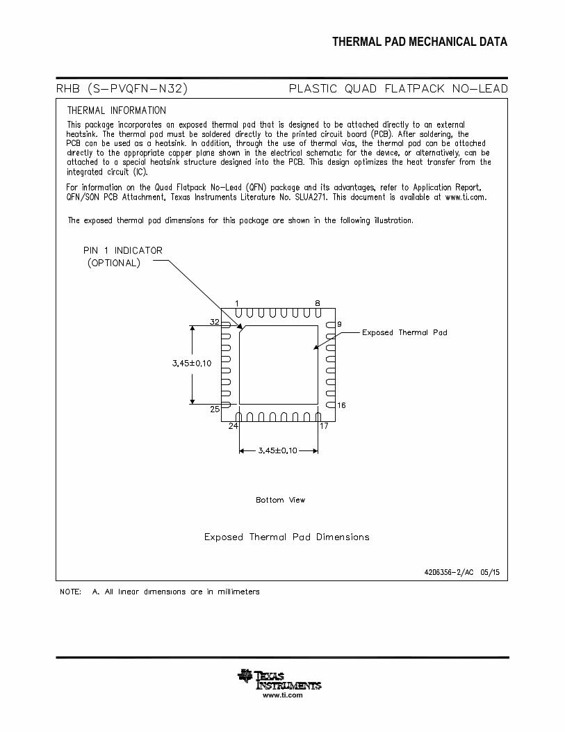


IMPORTANT NOTICE
Texas Instruments Incorporated and its subsidiaries (TI) reserve the right to make corrections, enhancements, improvements and otherchanges to its semiconductor products and services per JESD46, latest issue, and to discontinue any product or service per JESD48, latestissue. Buyers should obtain the latest relevant information before placing orders and should verify that such information is current andcomplete. All semiconductor products (also referred to herein as “components”) are sold subject to TI’s terms and conditions of salesupplied at the time of order acknowledgment.TI warrants performance of its components to the specifications applicable at the time of sale, in accordance with the warranty in TI’s termsand conditions of sale of semiconductor products. Testing and other quality control techniques are used to the extent TI deems necessaryto support this warranty. Except where mandated by applicable law, testing of all parameters of each component is not necessarilyperformed.TI assumes no liability for applications assistance or the design of Buyers’ products. Buyers are responsible for their products andapplications using TI components. To minimize the risks associated with Buyers’ products and applications, Buyers should provideadequate design and operating safeguards.TI does not warrant or represent that any license, either express or implied, is granted under any patent right, copyright, mask work right, orother intellectual property right relating to any combination, machine, or process in which TI components or services are used. Informationpublished by TI regarding third-party products or services does not constitute a license to use such products or services or a warranty orendorsement thereof. Use of such information may require a license from a third party under the patents or other intellectual property of thethird party, or a license from TI under the patents or other intellectual property of TI.Reproduction of significant portions of TI information in TI data books or data sheets is permissible only if reproduction is without alterationand is accompanied by all associated warranties, conditions, limitations, and notices. TI is not responsible or liable for such altereddocumentation. Information of third parties may be subject to additional restrictions.Resale of TI components or services with statements different from or beyond the parameters stated by TI for that component or servicevoids all express and any implied warranties for the associated TI component or service and is an unfair and deceptive business practice.TI is not responsible or liable for any such statements.Buyer acknowledges and agrees that it is solely responsible for compliance with all legal, regulatory and safety-related requirementsconcerning its products, and any use of TI components in its applications, notwithstanding any applications-related information or supportthat may be provided by TI. Buyer represents and agrees that it has all the necessary expertise to create and implement safeguards whichanticipate dangerous consequences of failures, monitor failures and their consequences, lessen the likelihood of failures that might causeharm and take appropriate remedial actions. Buyer will fully indemnify TI and its representatives against any damages arising out of the useof any TI components in safety-critical applications.In some cases, TI components may be promoted specifically to facilitate safety-related applications. With such components, TI’s goal is tohelp enable customers to design and create their own end-product solutions that meet applicable functional safety standards andrequirements. Nonetheless, such components are subject to these terms.No TI components are authorized for use in FDA Class III (or similar life-critical medical equipment) unless authorized officers of the partieshave executed a special agreement specifically governing such use.Only those TI components which TI has specifically designated as military grade or “enhanced plastic” are designed and intended for use inmilitary/aerospace applications or environments. Buyer acknowledges and agrees that any military or aerospace use of TI componentswhich have not been so designated is solely at the Buyer's risk, and that Buyer is solely responsible for compliance with all legal andregulatory requirements in connection with such use.TI has specifically designated certain components as meeting ISO/TS16949 requirements, mainly for automotive use. In any case of use ofnon-designated products, TI will not be responsible for any failure to meet ISO/TS16949.
Products ApplicationsAudio www.ti.com/audio Automotive and Transportation www.ti.com/automotiveAmplifiers amplifier.ti.com Communications and Telecom www.ti.com/communicationsData Converters dataconverter.ti.com Computers and Peripherals www.ti.com/computersDLP® Products www.dlp.com Consumer Electronics www.ti.com/consumer-appsDSP dsp.ti.com Energy and Lighting www.ti.com/energyClocks and Timers www.ti.com/clocks Industrial www.ti.com/industrialInterface interface.ti.com Medical www.ti.com/medicalLogic logic.ti.com Security www.ti.com/securityPower Mgmt power.ti.com Space, Avionics and Defense www.ti.com/space-avionics-defenseMicrocontrollers microcontroller.ti.com Video and Imaging www.ti.com/videoRFID www.ti-rfid.comOMAP Applications Processors www.ti.com/omap TI E2E Community e2e.ti.comWireless Connectivity www.ti.com/wirelessconnectivity
Mailing Address: Texas Instruments, Post Office Box 655303, Dallas, Texas 75265Copyright © 2015, Texas Instruments Incorporated