cascaded commutation circuit for a hybrid dc breaker … · 1 . cascaded commutation circuit for a...
TRANSCRIPT
1
Cascaded Commutation Circuit for a Hybrid DC Breaker with Dynamic
Control on Fault Current and DC Breaker Voltage
1Global Energy Interconnection Research Institute, Floor 9, Building B, Future Technology
Park, Changping District, Beijing 102200, People’s Republic of China 2Supply Design Ltd, Rosyth Business Centre, 16 Cromarty Campus, Rosyth, Fife, UK 3Department of Electronic & Electrical Engineering, Institute for Energy & Environment,
University of Strathclyde, Royal College Building,
This paper has not been submitted for journal or conference publication.
ABSTRACT This paper proposed a cascaded commutation circuit based on current commutation approach
for low-to-medium voltage DC fault current interruption, without snubber circuits, which slows
the fault current di/dt prior to current-zero and the rate of rise of the transient recovery voltage
dv/dt across the mechanical breaker contacts after current zero. The proposed dynamic control of
the fault current di/dt and circuit breaker voltage dVVCB/dt increase the fault current interruption
capability at the first and second current-zeros. Detailed mathematical equations are presented
to evaluate the operational waveform profile and the validity of the cascaded commutation
principle is confirmed by simulation and experimental results at 600Vdc, 110A and 330A.
Keywords: Hybrid DC Breaker, current commutation, current-zero, and fault interruption.
List of abbreviations ABB Asea Brown Boveri Ltd AC Alternating current CBs Circuit breakers 𝐶𝐶 Capacitance (F)
Yunhai Shan1
Tee C. Lim2
Stephen J. Finney3
Weixiao Guang1
[email protected] Barry W. Williams3
Derrick Holliday3 [email protected]
Xiao Ding1
2
𝐶𝐶𝐶𝐶 Commutation capacitance (F) 𝐶𝐶𝐶𝐶1,2,3 Cascaded commutation capacitance (F) 𝐶𝐶𝑠𝑠 Snubber capacitance (F) 𝐶𝐶𝑏𝑏𝑏𝑏𝑏𝑏𝑏𝑏 Capacitor bank (F) 𝑑𝑑𝑑𝑑 𝑑𝑑𝑑𝑑⁄ Decline rate of current before current-zero (kA/μs) 𝑑𝑑𝑑𝑑 𝑑𝑑𝑑𝑑⁄ Rise rate of voltage across the opening contacts immediately
after current-zero (kV/μs) 𝑑𝑑𝑑𝑑𝑉𝑉𝐶𝐶𝑉𝑉 𝑑𝑑𝑑𝑑⁄ Rise rate of voltage across the VCB immediately after
current-zero (kV/μs) DC Direct current HVDC High voltage direct current 𝑑𝑑𝐶𝐶1/2/3 Cascaded counter current (A) 𝑑𝑑𝑇𝑇 Current through the solid-state switches n Number of devices T1-T2-T3-T4-T5-T6 Solid-state switches TC1/2/3/4/5/6 Cascaded time intervals (μs) 𝑑𝑑𝐶𝐶𝐶𝐶1 Voltage cross the commutation capacitor 𝐶𝐶𝐶𝐶1 𝑑𝑑𝐶𝐶𝐶𝐶1,2 Voltage cross the series-connected commutation capacitor
𝐶𝐶𝐶𝐶1 and 𝐶𝐶𝐶𝐶2 𝑑𝑑𝐶𝐶𝐶𝐶1,2,3 Voltage cross the series-connected commutation capacitor
𝐶𝐶𝐶𝐶1, 𝐶𝐶𝐶𝐶2 and 𝐶𝐶𝐶𝐶3.

3
I. INTRODUCTION The necessity of DC breaker topologies in low to medium voltage applications is paramount to
the success of developing full DC systems either in localised grid infrastructure [1, 2] or
commercial applications in avionics, automotive and telecommunications [3]. Fast interruption
time, reliable and successful fault interruption are the main factors that contributes to the
system rating of the downstream power electronics. Over de-rating on the power electronics to
compromise on slow-switching DC breakers contributes to higher cost and lower efficiency
[4]. Arc-flash hazard analysis in low and medium voltage DC systems has been extensively
evaluated in [5, 6]. In particular to DC circuit breaker, arcing will occur when current-zero is
not achieved during the breaker interruption process [7, 8].
(a) Mechanical circuit breaker techniques
DC fault current limitation through helical arc control and mechanical circuit breaker has been
proposed in [9] and [10] respectively. Both studies utilise specific design on the mechanical
circuit breaker to either control the arc formation [9] or use of Thomson coil [10] to limit and
interrupt the fault current. However, the mechanical circuit breaker in [9] need to factor in the
large internal blades structure to enhance arc and fault current control. Allowing arc formation
can lead to subsequent structure failure and higher maintenance requirement. Although the
response time of the mechanical breaker in [10] is lesser than 2ms, the full interruption time
that is associated with the coil damping duration are larger than 10ms. This damping duration
need to be considered in rapid fault current interruption. The mechanical circuit breaker
technique in [11] demonstrated fast interruption time in micro-seconds range. The technique is
based on generating a reverse current and an intense axial magnetic field by two helical flux
compression generators. Although fast interruption time is achievable, the technique is limited
by low probability of successful fault interruption due to single current-zero generation and
reliability constraint by the requirement of significant magnetic field.
(b) Solid-state circuit breaker techniques
Alternate DC circuit breaker approaches that provide rapid fault current interruption has been
reviewed in [12-14]. These approaches are based on solid-state circuit breakers which depend
on the turning-off of the semiconductors to interrupt DC fault current. Fault current interruption
time lesser than 1ms can be achieved and the system structures are normally simple with lesser
components count. However, the main limiting factors that incurred with these approaches are
the on-state power losses and the cooling requirements that are associated with the
semiconductors. Although wide-band gap devices in [15, 16] has been proposed to reduce the

4
losses and cooling requirements, the semiconductors position on the DC line will need to
sustain the DC input voltage and the induced inductive voltage during fault current interruption.
High di/dt due to rapid fault current interruption will result in significant induced inductive
voltage. The semiconductors will have to be series-connected to sustain these overvoltage and
dynamic voltage sharing techniques [17] need to be integrated to prevent device failure.
(c) Hybrid circuit breaker techniques
The hybrid DC circuit breaker based on forced commutation principle has been extensively
research in HVDC applications [18-21]. The main principle underlying these approaches is to
introduce a current-zero to the mechanical circuit breaker before it attempts to interrupt the
fault current, thereby reducing the possibility of arcing and decreases the fault current
interruption time. Current-zero is achieved either through the series-connected semiconductor
device [18] with the mechanical circuit breaker or the forced current commutation from the
shunt-connected circuitry across the mechanical circuit breaker [19, 20]. The two stage
operation demonstrated in [21] commutated the fault current into the capacitor in a controlled
approach to achieve low voltage across the DC breaker during initial contact separation.
Although successful fault interruption can be achieved with reduce voltage across the DC
breaker as stated in [22], the semiconductors used in [21] need to be rated with respect to the
Metal Oxide Varistor (MOV) clamping voltage. MOV is used in the final stage to limit the
voltage across the DC breaker, which its clamping voltage can be twice of the DC input source.
The fault current interruption time from hybrid DC circuit breaker is dependent on the
mechanical circuit breaker opening under arc-less condition. These are generally longer than
solid-state circuit breaker techniques and also consists of circuitry with more components count
to achieve the current-zero condition. However, in DC applications where fault current
interruption time is between the range of 2 to 5ms [23], hybrid DC circuit breaker techniques
is preferred as the conduction loss is primarily dependent on the mechanical circuit breaker if
forced current commutation circuitry is shunt across the circuit breaker. This is much lower
than solid-state DC breaker and the physical disconnection of the current path is more reliable
with mechanical circuit breaker. Also, the cooling requirement for the semiconductors are less
as they are only operational during the fault condition.
The conditions associated with successful fault current interruption on DC circuit breaker has
been evaluated in [22]. A lower fault current di/dt or dVVCB/dt across the circuit breaker increase
the successful interruption probability. This paper enhances the work carried out in [22] and
proposed a cascaded forced current commutation circuitry that slows the fault current di/dt
prior to current-zero and a low dVVCB/dt voltage profile across the circuit breaker during the
5
interruption process. The volume and cost of the proposed commutation circuit can be reduced
with recent technological advances in power semiconductors devices [24, 25]. The availability
of 6.5kV IGBTs [26] allows lesser cascaded voltage stages and this made the proposed hybrid
DC circuit breaker well-suited in low to medium voltage level (1.2kV to 15kV) applications.
Applications in high voltage level (>15kV) can still be established with increased cascaded
voltage stages or utilizing next generation wide-band gap devices capable in excess of 10kV
voltage rating [16, 25, 27, 28]. However, the cost comparisons on the proposed approach with
others techniques and devices are not evaluated in this paper. The economic comparison on DC
breaker topologies is presented in [29].
This paper focus and evaluate on the approach and technique that allows the control of the fault
current di/dt and circuit breaker voltage dVVCB/dt. The test-rigs involved in the evaluation are
presented in [30].
Section II in this paper defines the operating principles of the proposed commutation circuit
with associated mathematical equations to confirm the waveform profiles. Section III presents
the simulation and experimental results of successful current interruption at 110A and 330A.
6
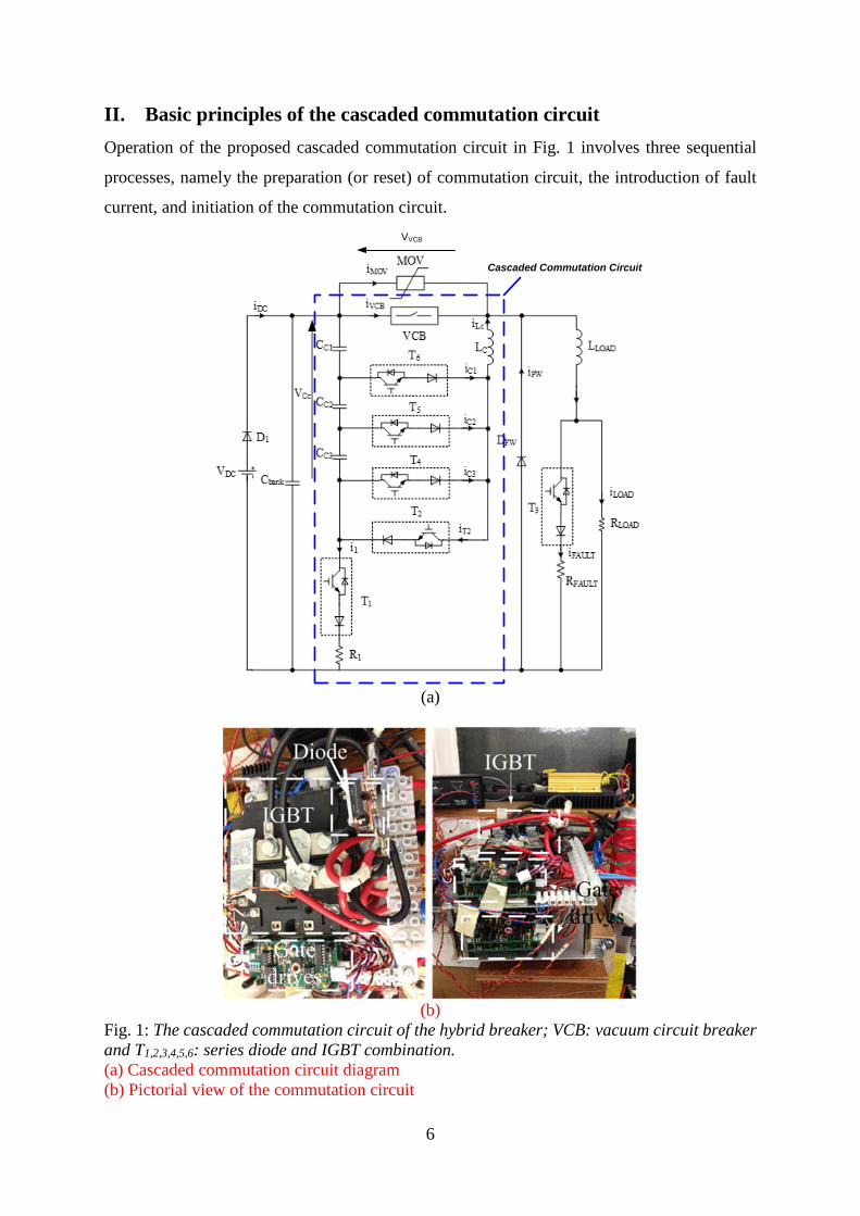
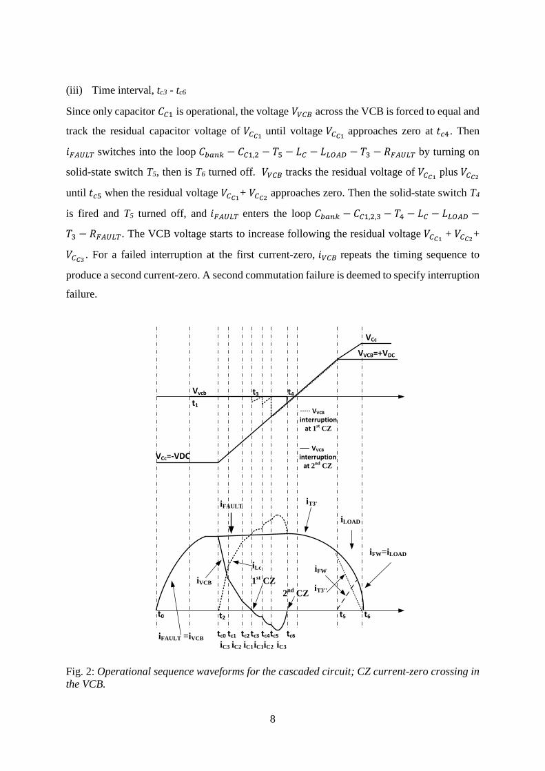
II. Basic principles of the cascaded commutation circuit Operation of the proposed cascaded commutation circuit in Fig. 1 involves three sequential
processes, namely the preparation (or reset) of commutation circuit, the introduction of fault
current, and initiation of the commutation circuit.
Cascaded Commutation Circuit
VVCB
(a)
(b)
Fig. 1: The cascaded commutation circuit of the hybrid breaker; VCB: vacuum circuit breaker and T1,2,3,4,5,6: series diode and IGBT combination. (a) Cascaded commutation circuit diagram (b) Pictorial view of the commutation circuit
7
The circuit consist of series-connected capacitors, such that 𝐶𝐶𝐶𝐶1 = 𝐶𝐶𝐶𝐶2 = 𝐶𝐶𝐶𝐶3 are in connection
with solid-state switches T4-T5-T6. The proposed circuitry allow n+1 capacitors to be connected
in series for higher DC voltage application and/or refined control of the dynamic dV/dt across
the VCB. In this paper, three capacitors are series-connected for the circuit analysis and
evaluation.
The three solid-state switches are controlled by sequential time intervals, overlapping for a
short duration (1μs in this paper) to ensure commutation current continuity, as shown in Fig.
3(H). Under normal load conditions, only the VCB and T1 are closed, transmitting power to
load and to charge the commutation capacitors 𝐶𝐶𝐶𝐶1 − 𝐶𝐶𝐶𝐶2 − 𝐶𝐶𝐶𝐶3 with an initial voltage totalling
𝑑𝑑𝐷𝐷𝐶𝐶, respectively while the other switches, T2 to T6, are open. A DC fault is emulated by turning
on T3, so that the energy stored in the capacitor bank 𝐶𝐶𝑏𝑏𝑏𝑏𝑏𝑏𝑏𝑏 is released through the load inductor
𝐿𝐿𝐿𝐿𝐿𝐿𝐿𝐿𝐷𝐷 into the fault resistor 𝑅𝑅𝐹𝐹𝐿𝐿𝐹𝐹𝐿𝐿𝑇𝑇, to produce a high current through the VCB before the
electrodes open. For commutation preparation, the commutation capacitors 𝐶𝐶𝐶𝐶1,2,3 are reversed
charged by turning on T2 after receiving the trip signal. Since 𝐶𝐶𝐶𝐶1 = 𝐶𝐶𝐶𝐶2 = 𝐶𝐶𝐶𝐶3, the voltage
cross each capacitor is equal (𝑑𝑑𝐶𝐶𝐶𝐶1 = 𝑑𝑑𝐶𝐶𝐶𝐶2 = 𝑑𝑑𝐶𝐶𝐶𝐶3). The fault clearance interruption procedure
is shown in Fig. 2. For analysis convenience, the VCB arc voltage is ignored, being a low
voltage.
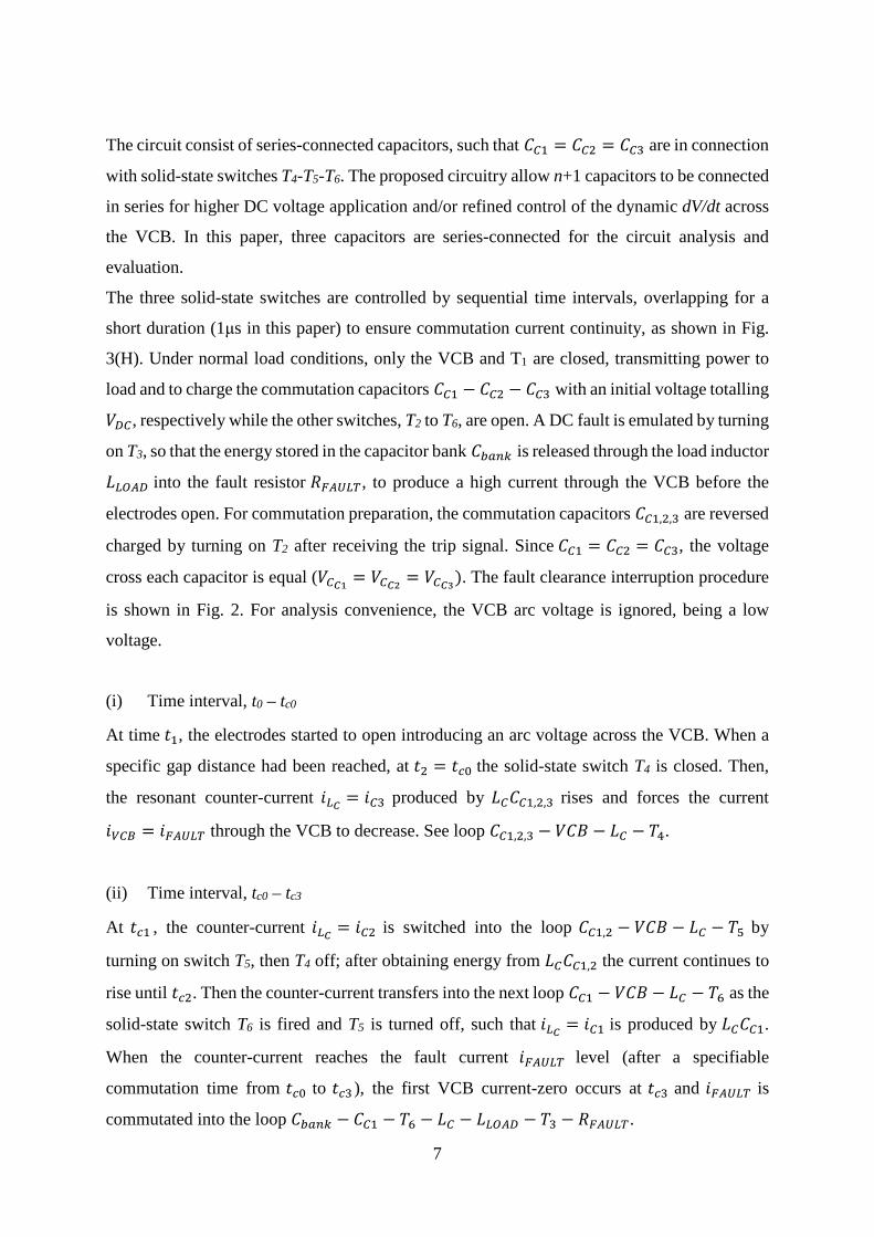
(i) Time interval, t0 – tc0
At time 𝑑𝑑1, the electrodes started to open introducing an arc voltage across the VCB. When a
specific gap distance had been reached, at 𝑑𝑑2 = 𝑑𝑑𝑐𝑐0 the solid-state switch T4 is closed. Then,
the resonant counter-current 𝑑𝑑𝐿𝐿𝐶𝐶 = 𝑑𝑑𝐶𝐶3 produced by 𝐿𝐿𝐶𝐶𝐶𝐶𝐶𝐶1,2,3 rises and forces the current
𝑑𝑑𝑉𝑉𝐶𝐶𝑉𝑉 = 𝑑𝑑𝐹𝐹𝐿𝐿𝐹𝐹𝐿𝐿𝑇𝑇 through the VCB to decrease. See loop 𝐶𝐶𝐶𝐶1,2,3 − 𝑑𝑑𝐶𝐶𝑉𝑉 − 𝐿𝐿𝐶𝐶 − 𝑇𝑇4.
(ii) Time interval, tc0 – tc3
At 𝑑𝑑𝑐𝑐1 , the counter-current 𝑑𝑑𝐿𝐿𝐶𝐶 = 𝑑𝑑𝐶𝐶2 is switched into the loop 𝐶𝐶𝐶𝐶1,2 − 𝑑𝑑𝐶𝐶𝑉𝑉 − 𝐿𝐿𝐶𝐶 − 𝑇𝑇5 by
turning on switch T5, then T4 off; after obtaining energy from 𝐿𝐿𝐶𝐶𝐶𝐶𝐶𝐶1,2 the current continues to
rise until 𝑑𝑑𝑐𝑐2. Then the counter-current transfers into the next loop 𝐶𝐶𝐶𝐶1 − 𝑑𝑑𝐶𝐶𝑉𝑉 − 𝐿𝐿𝐶𝐶 − 𝑇𝑇6 as the
solid-state switch T6 is fired and T5 is turned off, such that 𝑑𝑑𝐿𝐿𝐶𝐶 = 𝑑𝑑𝐶𝐶1 is produced by 𝐿𝐿𝐶𝐶𝐶𝐶𝐶𝐶1.
When the counter-current reaches the fault current 𝑑𝑑𝐹𝐹𝐿𝐿𝐹𝐹𝐿𝐿𝑇𝑇 level (after a specifiable
commutation time from 𝑑𝑑𝑐𝑐0 to 𝑑𝑑𝑐𝑐3 ), the first VCB current-zero occurs at 𝑑𝑑𝑐𝑐3 and 𝑑𝑑𝐹𝐹𝐿𝐿𝐹𝐹𝐿𝐿𝑇𝑇 is
commutated into the loop 𝐶𝐶𝑏𝑏𝑏𝑏𝑏𝑏𝑏𝑏 − 𝐶𝐶𝐶𝐶1 − 𝑇𝑇6 − 𝐿𝐿𝐶𝐶 − 𝐿𝐿𝐿𝐿𝐿𝐿𝐿𝐿𝐷𝐷 − 𝑇𝑇3 − 𝑅𝑅𝐹𝐹𝐿𝐿𝐹𝐹𝐿𝐿𝑇𝑇.
8
(iii) Time interval, tc3 - tc6
Since only capacitor 𝐶𝐶𝐶𝐶1 is operational, the voltage 𝑑𝑑𝑉𝑉𝐶𝐶𝑉𝑉 across the VCB is forced to equal and
track the residual capacitor voltage of 𝑑𝑑𝐶𝐶𝐶𝐶1 until voltage 𝑑𝑑𝐶𝐶𝐶𝐶1 approaches zero at 𝑑𝑑𝑐𝑐4 . Then
𝑑𝑑𝐹𝐹𝐿𝐿𝐹𝐹𝐿𝐿𝑇𝑇 switches into the loop 𝐶𝐶𝑏𝑏𝑏𝑏𝑏𝑏𝑏𝑏 − 𝐶𝐶𝐶𝐶1,2 − 𝑇𝑇5 − 𝐿𝐿𝐶𝐶 − 𝐿𝐿𝐿𝐿𝐿𝐿𝐿𝐿𝐷𝐷 − 𝑇𝑇3 − 𝑅𝑅𝐹𝐹𝐿𝐿𝐹𝐹𝐿𝐿𝑇𝑇 by turning on
solid-state switch T5, then is T6 turned off. 𝑑𝑑𝑉𝑉𝐶𝐶𝑉𝑉 tracks the residual voltage of 𝑑𝑑𝐶𝐶𝐶𝐶1 plus 𝑑𝑑𝐶𝐶𝐶𝐶2
until 𝑑𝑑𝑐𝑐5 when the residual voltage 𝑑𝑑𝐶𝐶𝐶𝐶1+ 𝑑𝑑𝐶𝐶𝐶𝐶2 approaches zero. Then the solid-state switch T4
is fired and T5 turned off, and 𝑑𝑑𝐹𝐹𝐿𝐿𝐹𝐹𝐿𝐿𝑇𝑇 enters the loop 𝐶𝐶𝑏𝑏𝑏𝑏𝑏𝑏𝑏𝑏 − 𝐶𝐶𝐶𝐶1,2,3 − 𝑇𝑇4 − 𝐿𝐿𝐶𝐶 − 𝐿𝐿𝐿𝐿𝐿𝐿𝐿𝐿𝐷𝐷 −
𝑇𝑇3 − 𝑅𝑅𝐹𝐹𝐿𝐿𝐹𝐹𝐿𝐿𝑇𝑇. The VCB voltage starts to increase following the residual voltage 𝑑𝑑𝐶𝐶𝐶𝐶1 + 𝑑𝑑𝐶𝐶𝐶𝐶2+
𝑑𝑑𝐶𝐶𝐶𝐶3 . For a failed interruption at the first current-zero, 𝑑𝑑𝑉𝑉𝐶𝐶𝑉𝑉 repeats the timing sequence to
produce a second current-zero. A second commutation failure is deemed to specify interruption
failure.
Fig. 2: Operational sequence waveforms for the cascaded circuit; CZ current-zero crossing in the VCB.
t0 t2
t3
1st CZ2nd CZ
iFAULT =iVCB
iVCB
iFAULT
iLc iFW
t1
iT3'
VCc=-VDC
VVCB=+VDC
VCc
t4
t5 t6
iT3''
iLOAD
iFW=iLOAD
Vvcb
VVCB interruption
at 1st CZ
VVCB interruption
at 2nd CZ
tc0 tc1 tc2 tc3 tc4tc5 tc6
iC3 iC2 iC1iC1iC2 iC3

9
Cbank
CC1 LCVCB
LLOAD
RFAULT
T6
T5
T3
iVCB
iC1
iC2
T4iC3
CC2
CC3
(A) (B)
iFAULT Cbank
CC1 LCVCB
LLOAD
RFAULT
T3
iVCB
iC1
iC2
T4iC3
CC2
CC3
iFAULT
iLc iLc
Cbank
CC1 LCVCB
LLOAD
RFAULT
T5
T3
iVCB
iC1
iC2
iC3
CC2
CC3
iFAULTCbank
CC1 LCVCB
LLOAD
RFAULT
T6
T3
iVCB
iC1
iC2
iC3
CC2
CC3
iFAULT
(C) (D)
iLciLc
Cbank
CC1 LC LLOAD
RFAULT
T6
T3
iC1
iC2
iC3
CC2
CC3
iLc
iFAULT Cbank
CC1 LC LLOAD
RFAULT
T3
iC1
iC2
iC3
CC2
CC3
iLc
T5
iFAULT
(E) (F)
10
Fig. 3: Interruption sequence of the cascaded commutation circuit.
The mathematical description of the interruption sequences during commutation is based on
the timing diagram in Fig. 3. For simplified analysis, the inductors are assumed linear, the
voltage drops across all solid-state switches and the VCB state are zero during the on-state; due
to large 𝐶𝐶𝑏𝑏𝑏𝑏𝑏𝑏𝑏𝑏, its voltage is considered constant, charged to 𝑑𝑑𝐷𝐷𝐶𝐶; the commutation capacitors
have no circuit leakage paths when inactive; and finally, the VCB fault current 𝑑𝑑𝐹𝐹𝐿𝐿𝐹𝐹𝐿𝐿𝑇𝑇 is
unchanged during the commutation process, since the commutation time is shorter than the
fault-path time constant. A detailed solution is obtained by solving the differential equations
corresponding to each interval; while the end state of one interval is the initial state of the
following interval, thereby maintaining continuity between successive intervals.
(A) Prior to commutation circuit operation
Fig. 3(A) depicts the cascaded circuit when the VCB fault current has reached its expected
value. The VCB electrodes have separated a specific distance. The commutation capacitor
𝐶𝐶𝐶𝐶1,2,3 has been reversed charging, so that the commutation circuit is ready to produce a
counter-current through the VCB. In Fig. 3(H), to maintain cascaded commutation circuit
continuity, solid-state switches T4-T5-T6 are controlled through a sequence of six intervals with
1μs overlapping (intervals TC1-TC2-TC3-TC4-TC5-TC6). Intervals TC3 and TC4 use the same signal.
Overlap ensures continuity, that is 𝑑𝑑𝑐𝑐1 = 𝑑𝑑𝑐𝑐1_, 𝑑𝑑𝑐𝑐2 = 𝑑𝑑𝑐𝑐2_, 𝑑𝑑𝑐𝑐4 = 𝑑𝑑𝑐𝑐4_, 𝑑𝑑𝑐𝑐5 = 𝑑𝑑𝑐𝑐5_.
T4
T5
T6
0
0
0
tC0 tC1
tC1_ tC2
tC2_ tC3 tC4
tC4_ tC5
tC5_ tC6 t5 t6... ... ... t
t
t
(B)
(C)
(D) (E)
(F)
(G)
TC1
TC2
TC3 TC4
TC5
1μs overlapping
Cbank
CC1 LC LLOAD
RFAULT
T3
iC1
iC2
iC3
CC2
CC3
iLc
T4
iFAULT
(G) (H)
11
(B) Time interval, 𝑑𝑑𝑐𝑐0 ≤ 𝑑𝑑 ≤ 𝑑𝑑𝑐𝑐1
At time 𝑑𝑑2 = 𝑑𝑑𝑐𝑐0, switch T4 is turned on to introduce counter-current 𝑑𝑑𝐿𝐿𝐶𝐶 through the VCB,
forcing the current 𝑑𝑑𝑉𝑉𝐶𝐶𝑉𝑉 through the VCB to decrease. The relationships between 𝑑𝑑𝐹𝐹𝐿𝐿𝐹𝐹𝐿𝐿𝑇𝑇 , 𝑑𝑑𝑉𝑉𝐶𝐶𝑉𝑉
and 𝑑𝑑𝐶𝐶 is:
𝑑𝑑𝐹𝐹𝐿𝐿𝐹𝐹𝐿𝐿𝑇𝑇 = 𝑑𝑑𝑉𝑉𝐶𝐶𝑉𝑉 + 𝑑𝑑𝐿𝐿𝐶𝐶 (A) (1)
where𝑑𝑑𝐿𝐿𝐶𝐶 = 𝑑𝑑𝐶𝐶3 and𝐶𝐶𝐶𝐶1 = 𝐶𝐶𝐶𝐶2 = 𝐶𝐶𝐶𝐶2, thus the current 𝑑𝑑𝐶𝐶3 through circuit loop 𝐶𝐶𝐶𝐶1,2,3 − 𝑑𝑑𝐶𝐶𝑉𝑉 −
𝐿𝐿𝐶𝐶 − 𝑇𝑇4 is defined by:
1𝐶𝐶𝐶𝐶1,2,3
𝑑𝑑𝐶𝐶3𝑑𝑑𝑑𝑑 + 𝐿𝐿𝐶𝐶𝑑𝑑𝑑𝑑𝐶𝐶3𝑑𝑑𝑑𝑑
= 0 (2)
with the initial conditions
𝑑𝑑𝐶𝐶3(𝑑𝑑𝑐𝑐0) = 0 (A) and 𝑑𝑑𝐶𝐶𝐶𝐶(𝑑𝑑𝑐𝑐0) = −𝑑𝑑𝐷𝐷𝐶𝐶 (V)
which yield:
𝑑𝑑𝐶𝐶3(𝑑𝑑) = 𝑉𝑉𝐷𝐷𝐶𝐶𝑍𝑍
sin𝜔𝜔0𝑑𝑑 (A) (3)
and 𝑑𝑑𝐶𝐶𝐶𝐶1,2,3(𝑑𝑑) = −𝑑𝑑𝐷𝐷𝐶𝐶 cos𝜔𝜔0𝑑𝑑 (V) (4)
0 ≤ 𝜔𝜔0𝑑𝑑 ≤ 𝜋𝜋 (rad)
where 𝜔𝜔0 = 1 𝐿𝐿𝐶𝐶𝐶𝐶𝐶𝐶1,2,3⁄ (rad/s)
𝑍𝑍 = 𝐿𝐿𝐶𝐶 𝐶𝐶𝐶𝐶1,2,3⁄ (Ω)
𝐶𝐶𝐶𝐶1,2,3 = ⅓𝐶𝐶𝐶𝐶1 = ⅓𝐶𝐶𝐶𝐶2 = ⅓𝐶𝐶𝐶𝐶3 (F)
At the end of this interval, the voltage across the commutation capacitors 𝐶𝐶𝐶𝐶1,2,3 is 𝑑𝑑𝐶𝐶𝐶𝐶1,2,3 =
𝑑𝑑𝐶𝐶𝐶𝐶1,2,3(𝑑𝑑𝑐𝑐1), that is 𝑑𝑑𝐶𝐶𝐶𝐶1 = 𝑑𝑑𝐶𝐶𝐶𝐶2 = 𝑑𝑑𝐶𝐶𝐶𝐶3 = ⅓𝑑𝑑𝐶𝐶𝐶𝐶1,2,3(𝑑𝑑𝑐𝑐1); and the commutation current is 𝑑𝑑𝐶𝐶 =
𝑑𝑑𝐶𝐶3(𝑑𝑑𝑐𝑐1); thus the equation describing this interval 𝑇𝑇𝐶𝐶1 is:
𝑇𝑇𝐶𝐶1=𝑑𝑑𝑐𝑐1 − 𝑑𝑑𝑐𝑐0 =−sin−1𝑖𝑖𝐶𝐶3
(𝑡𝑡𝑐𝑐1)𝑍𝑍𝑉𝑉𝐷𝐷𝐶𝐶
𝜔𝜔0 (5)
(C) Time interval, 𝑑𝑑𝑐𝑐1 ≤ 𝑑𝑑 ≤ 𝑑𝑑𝑐𝑐2
T5 is turned on and T4 off at 𝑑𝑑𝑐𝑐1, then the commutation current 𝑑𝑑𝐿𝐿𝐶𝐶 diverts into the loop 𝐶𝐶𝐶𝐶1,2 −
𝑑𝑑𝐶𝐶𝑉𝑉 − 𝐿𝐿𝐶𝐶 − 𝑇𝑇5; thus equalling current 𝑑𝑑𝐶𝐶2 which can be expressed by the differential equation:
1𝐶𝐶𝐶𝐶1,2
𝑑𝑑𝐶𝐶2𝑑𝑑𝑑𝑑 + 𝐿𝐿𝐶𝐶𝑑𝑑𝑑𝑑𝐶𝐶2𝑑𝑑𝑑𝑑
= 0 (6)
with initial conditions
𝑑𝑑𝐶𝐶2(𝑑𝑑𝑐𝑐1) = 𝑑𝑑𝐶𝐶3(𝑑𝑑𝑐𝑐1) (A) and 𝑑𝑑𝐶𝐶𝐶𝐶1,2(𝑑𝑑𝑐𝑐1) = ⅔𝑑𝑑𝐶𝐶𝐶𝐶1,2,3(𝑑𝑑𝑐𝑐1) (V)

12
which yield:
𝑑𝑑𝐶𝐶2(𝑑𝑑) = 𝑑𝑑𝐶𝐶3(𝑑𝑑𝑐𝑐1) cos𝜔𝜔0′𝑑𝑑 −2𝑉𝑉𝐶𝐶𝐶𝐶1,2,3(𝑡𝑡𝑐𝑐1)
3𝑍𝑍′sin𝜔𝜔0′𝑑𝑑 (A) (7)
and 𝑑𝑑𝐶𝐶𝐶𝐶1,2,(𝑑𝑑) = 𝑍𝑍′𝑖𝑖𝐶𝐶3(𝑑𝑑𝑐𝑐1) sin𝜔𝜔0′𝑑𝑑 + ⅔𝑑𝑑𝐶𝐶𝐶𝐶1,2,3(𝑑𝑑𝑐𝑐1)cos𝜔𝜔0𝑑𝑑 (V) (8)
0 ≤ 𝜔𝜔0𝑑𝑑 ≤ 𝜋𝜋 (rad)
where 𝜔𝜔0′ = 1 𝐿𝐿𝐶𝐶𝐶𝐶𝐶𝐶1,2⁄ (rad/s)
𝑍𝑍′ = 𝐿𝐿𝐶𝐶 𝐶𝐶𝐶𝐶1,2⁄ (Ω)
𝐶𝐶𝐶𝐶1,2 = ½𝐶𝐶𝐶𝐶1 = ½𝐶𝐶𝐶𝐶2 = ½𝐶𝐶𝐶𝐶3 (F)
At the end of this interval, the voltage across the commutation capacitor 𝐶𝐶𝐶𝐶1,2 is 𝑑𝑑𝐶𝐶𝐶𝐶1,2 =
𝑑𝑑𝐶𝐶𝐶𝐶1,2,(𝑑𝑑𝑐𝑐2), where 𝑑𝑑𝐶𝐶𝐶𝐶1 = 𝑑𝑑𝐶𝐶𝐶𝐶2 = ½𝑑𝑑𝐶𝐶𝐶𝐶1,2(𝑑𝑑𝑐𝑐2), 𝑑𝑑𝐶𝐶𝐶𝐶3 = ⅓𝑑𝑑𝐶𝐶𝐶𝐶1,2,3(𝑑𝑑𝑐𝑐1); and the commutation
current is 𝑑𝑑𝐿𝐿𝐶𝐶 = 𝑑𝑑𝐶𝐶2(𝑑𝑑𝑐𝑐2); thus the equation for the time of this interval 𝑇𝑇𝐶𝐶2 is:
𝑇𝑇𝐶𝐶2=𝑑𝑑𝑐𝑐2 − 𝑑𝑑𝑐𝑐1 =
−sin−1𝑉𝑉𝐶𝐶𝐶𝐶1,2(𝑡𝑡𝑐𝑐1)×𝑖𝑖𝐶𝐶2(𝑡𝑡𝑐𝑐2)+𝐿𝐿𝐶𝐶×𝑖𝑖𝐶𝐶2(𝑡𝑡𝑐𝑐1)×𝜔𝜔0′×𝐴𝐴
(𝐶𝐶𝐶𝐶1,2×𝑉𝑉𝐶𝐶𝐶𝐶1,2(𝑡𝑡𝑐𝑐1)
2+𝐿𝐿𝐶𝐶×𝑖𝑖𝐶𝐶2(𝑡𝑡𝑐𝑐1)
2)×𝜔𝜔0′
𝜔𝜔0′
(9)
where 𝐴𝐴 = 𝐶𝐶𝐶𝐶1,2×(𝑉𝑉𝐶𝐶𝐶𝐶1,2(𝑡𝑡𝑐𝑐1))2+𝐿𝐿𝐶𝐶×(𝑖𝑖𝐶𝐶2(𝑡𝑡𝑐𝑐1))2−𝐿𝐿𝑐𝑐×(𝑖𝑖𝐶𝐶2(𝑡𝑡𝑐𝑐2))2
𝐿𝐿𝐶𝐶
(D) Time interval,𝑑𝑑𝑐𝑐2 ≤ 𝑑𝑑 ≤ 𝑑𝑑𝑐𝑐3
Solid-state switch T6 is fired and T5 is turned off at time 𝑑𝑑𝑐𝑐2, then the commutation current 𝑑𝑑𝐿𝐿𝐶𝐶
enters the loop 𝐶𝐶𝐶𝐶1 − 𝑑𝑑𝐶𝐶𝑉𝑉 − 𝐿𝐿𝐶𝐶 − 𝑇𝑇6. The resulting current 𝑑𝑑𝐶𝐶1 is defined by:
1𝐶𝐶𝐶𝐶1
𝑑𝑑𝐶𝐶1𝑑𝑑𝑑𝑑 + 𝐿𝐿𝐶𝐶𝑑𝑑𝑑𝑑𝐶𝐶1𝑑𝑑𝑑𝑑
= 0 (10)
with the initial conditions
𝑑𝑑𝐶𝐶1(𝑑𝑑𝑐𝑐2) = 𝑑𝑑𝐶𝐶2(𝑑𝑑𝑐𝑐2) (A) and 𝑑𝑑𝐶𝐶𝐶𝐶1(𝑑𝑑𝑐𝑐2) =𝑉𝑉𝐶𝐶𝐶𝐶1,2(𝑡𝑡𝑐𝑐2)
2 (V)
which yield:
𝑑𝑑𝐶𝐶1(𝑑𝑑) = 𝑑𝑑𝐶𝐶2(𝑑𝑑𝑐𝑐2) cos𝜔𝜔0′′𝑑𝑑 −𝑉𝑉𝐶𝐶𝐶𝐶1,2(𝑡𝑡𝑐𝑐2)
2𝑍𝑍′′sin𝜔𝜔0′′𝑑𝑑 (A) (11)
and 𝑑𝑑𝐶𝐶𝐶𝐶1(𝑑𝑑) = 𝑍𝑍′′𝑑𝑑𝐶𝐶2(𝑑𝑑𝑐𝑐2) sin𝜔𝜔0′′𝑑𝑑 +𝑉𝑉𝐶𝐶𝐶𝐶1,2(𝑡𝑡𝑐𝑐2)
2 cos𝜔𝜔0′′𝑑𝑑 (V) (12)
0 ≤ 𝜔𝜔0𝑑𝑑 ≤ 𝜋𝜋 (rad)
where 𝜔𝜔0′′ = 1 𝐿𝐿𝐶𝐶𝐶𝐶𝐶𝐶1⁄ (rad/s)
𝑍𝑍′′ = 𝐿𝐿𝐶𝐶 𝐶𝐶𝐶𝐶1⁄ (Ω)
𝐶𝐶𝐶𝐶1 = 𝐶𝐶𝐶𝐶2 = 𝐶𝐶𝐶𝐶3 (F)
13
When the commutation current 𝑑𝑑𝐶𝐶1 rises to equal the fault current, in the commutation period
𝑑𝑑𝑐𝑐0 to 𝑑𝑑𝑐𝑐3, there is sufficient time for vacuum recovery, having introduced a VCB current-zero.
Since the period of each interval has been calculated, it is possible to achieve the first current-
zero occurring at time 𝑑𝑑𝑐𝑐3. This means 𝑑𝑑𝐶𝐶1(𝑑𝑑𝑐𝑐3)=𝑑𝑑𝐹𝐹𝐿𝐿𝐹𝐹𝐿𝐿𝑇𝑇(𝑑𝑑𝑐𝑐3) and the commutation capacitor
𝐶𝐶𝐶𝐶1voltage is 𝑑𝑑𝐶𝐶𝐶𝐶1 = 𝑑𝑑𝐶𝐶𝐶𝐶1(𝑑𝑑𝑐𝑐3), and the other capacitor voltages are 𝑑𝑑𝐶𝐶𝐶𝐶2 = ½𝑑𝑑𝐶𝐶𝐶𝐶1,2(𝑑𝑑𝑐𝑐2) and
𝑑𝑑𝐶𝐶𝐶𝐶3 = ⅓𝑑𝑑𝐶𝐶𝐶𝐶1,2,3(𝑑𝑑𝑐𝑐1). The period of this interval 𝑇𝑇𝐶𝐶3 is:
𝑇𝑇𝐶𝐶3=𝑑𝑑𝑐𝑐3 − 𝑑𝑑𝑐𝑐2 =
−sin−1𝑉𝑉𝐶𝐶𝐶𝐶1(𝑡𝑡𝑐𝑐1)×𝑖𝑖𝐹𝐹𝐴𝐴𝐹𝐹𝐿𝐿𝐹𝐹(𝑡𝑡𝑐𝑐3)+𝐿𝐿𝐶𝐶×𝑖𝑖𝐶𝐶1(𝑡𝑡𝑐𝑐2)×𝜔𝜔0′′×𝐴𝐴′
(𝐶𝐶𝐶𝐶1×𝑉𝑉𝐶𝐶𝐶𝐶1(𝑡𝑡𝑐𝑐2)
2+𝐿𝐿𝐶𝐶×𝑖𝑖𝐶𝐶1(𝑡𝑡𝑐𝑐2)
2)×𝜔𝜔0′′
𝜔𝜔0′′
(13)
where 𝐴𝐴′ = 𝐶𝐶𝐶𝐶1×(𝑉𝑉𝐶𝐶𝐶𝐶1(𝑡𝑡𝑐𝑐1))2+𝐿𝐿𝐶𝐶×(𝑖𝑖𝐶𝐶1(𝑡𝑡𝑐𝑐2))2−𝐿𝐿𝑐𝑐×(𝑖𝑖𝐹𝐹𝐴𝐴𝐹𝐹𝐿𝐿𝐹𝐹(𝑡𝑡𝑐𝑐3))2
𝐿𝐿𝐶𝐶
In summary, the commutation current 𝑑𝑑𝐿𝐿𝐶𝐶 , before current-zero, can be described by the
piecewise function:
𝑑𝑑𝐶𝐶 =
⎩⎪⎪⎨
⎪⎪⎧ 𝑑𝑑𝐶𝐶3(𝑑𝑑)𝑑𝑑𝐶𝐶3(𝑑𝑑) =
𝑑𝑑𝐷𝐷𝐶𝐶𝑍𝑍
sin𝜔𝜔0𝑑𝑑 (𝑑𝑑𝑐𝑐0 ≤ 𝑑𝑑 ≤ 𝑑𝑑𝑐𝑐1)
𝑑𝑑𝐶𝐶2(𝑑𝑑) = 𝑑𝑑𝐶𝐶3(𝑑𝑑𝑐𝑐1) cos𝜔𝜔0′𝑑𝑑 −2𝑑𝑑𝐶𝐶𝐶𝐶1,2,3(𝑑𝑑𝑐𝑐1)
3𝑍𝑍′sin𝜔𝜔0′𝑑𝑑 (𝑑𝑑𝑐𝑐1 ≤ 𝑑𝑑 ≤ 𝑑𝑑𝑐𝑐2)
𝑑𝑑𝐶𝐶1(𝑑𝑑) = 𝑑𝑑𝐶𝐶2(𝑑𝑑𝑐𝑐2) cos𝜔𝜔0′′𝑑𝑑 −𝑑𝑑𝐶𝐶𝐶𝐶1,2(𝑑𝑑𝑐𝑐2)
2𝑍𝑍′′sin𝜔𝜔0′′𝑑𝑑 (𝑑𝑑𝑐𝑐2 ≤ 𝑑𝑑 ≤ 𝑑𝑑𝑐𝑐3) ⎭
⎪⎪⎬
⎪⎪⎫
(14)
(E) Time interval,𝑑𝑑𝑐𝑐3 ≤ 𝑑𝑑 ≤ 𝑑𝑑𝑐𝑐4
𝑑𝑑𝐹𝐹𝐿𝐿𝐹𝐹𝐿𝐿𝑇𝑇 is commutated into the loop 𝐶𝐶𝑏𝑏𝑏𝑏𝑏𝑏𝑏𝑏 − 𝐶𝐶𝐶𝐶1 − 𝑇𝑇6 − 𝐿𝐿𝐶𝐶 − 𝐿𝐿𝐿𝐿𝐿𝐿𝐿𝐿𝐷𝐷 − 𝑇𝑇3 − 𝑅𝑅𝐹𝐹𝐿𝐿𝐹𝐹𝐿𝐿𝑇𝑇; but is still
equal to 𝑑𝑑𝐶𝐶1 which can be expressed by the differential equation:
1𝐶𝐶𝐶𝐶1
𝑑𝑑𝐶𝐶1𝑑𝑑𝑑𝑑 + 𝐿𝐿𝐶𝐶𝑑𝑑𝑑𝑑𝐶𝐶1𝑑𝑑𝑑𝑑
+ 𝐿𝐿𝐿𝐿𝐿𝐿𝐿𝐿𝐷𝐷𝑑𝑑𝑑𝑑𝐶𝐶1𝑑𝑑𝑑𝑑
+ 𝑑𝑑𝐶𝐶1𝑅𝑅𝐹𝐹𝐿𝐿𝐹𝐹𝐿𝐿𝑇𝑇 = 𝑑𝑑𝐷𝐷𝐶𝐶 (15)
where the voltage across 𝐶𝐶𝑏𝑏𝑏𝑏𝑏𝑏𝑏𝑏 can be considered a DC source due to large 𝐶𝐶𝑏𝑏𝑏𝑏𝑏𝑏𝑏𝑏, with
the initial conditions
𝑑𝑑𝐶𝐶1(𝑑𝑑𝑐𝑐3)=𝑑𝑑𝐹𝐹𝐿𝐿𝐹𝐹𝐿𝐿𝑇𝑇(𝑑𝑑𝑐𝑐3)(A) and 𝑑𝑑𝐶𝐶𝐶𝐶1 = 𝑑𝑑𝐶𝐶𝐶𝐶1(𝑑𝑑𝑐𝑐3) (V)
Practically 𝑅𝑅𝐹𝐹𝐿𝐿𝐹𝐹𝐿𝐿𝑇𝑇 < 2𝐿𝐿𝐿𝐿𝐿𝐿𝐴𝐴𝐷𝐷𝐶𝐶𝐶𝐶1
, which yields:
𝑑𝑑𝐶𝐶1(𝑑𝑑) = 2𝐾𝐾1′𝑒𝑒−𝛿𝛿2𝑡𝑡 cos(𝜔𝜔3′𝑑𝑑 − 𝜃𝜃′) (A) (16)
𝑑𝑑𝐶𝐶𝐶𝐶1(𝑑𝑑) = 2𝐾𝐾1′𝐶𝐶𝐶𝐶1𝜔𝜔4′
[cos(𝛽𝛽2′ − 𝜃𝜃′) −𝑒𝑒−𝛿𝛿2𝑡𝑡 cos(𝜔𝜔3′𝑑𝑑 − 𝜃𝜃′ + 𝛽𝛽2′)] +𝑑𝑑𝐶𝐶𝐶𝐶1(𝑑𝑑𝑐𝑐3) (V) (17)
where 𝛿𝛿2 = 𝑅𝑅𝐹𝐹𝐴𝐴𝐹𝐹𝐿𝐿𝐹𝐹2(𝐿𝐿𝐿𝐿𝐿𝐿𝐴𝐴𝐷𝐷+𝐿𝐿𝐶𝐶)
; 𝜔𝜔3′2 = 1
(𝐿𝐿𝐿𝐿𝐿𝐿𝐴𝐴𝐷𝐷+𝐿𝐿𝐶𝐶)𝐶𝐶𝐶𝐶1− 𝑅𝑅𝐹𝐹𝐴𝐴𝐹𝐹𝐿𝐿𝐹𝐹
2(𝐿𝐿𝐿𝐿𝐿𝐿𝐴𝐴𝐷𝐷+𝐿𝐿𝐶𝐶)2
𝜔𝜔4′ = 𝛿𝛿22 + 𝜔𝜔3′2 ; 𝛽𝛽2′ = tan−1 𝜔𝜔3′
𝛿𝛿2

14
𝐾𝐾1′ = (𝑑𝑑𝐹𝐹𝐿𝐿𝐹𝐹𝐿𝐿𝑇𝑇(𝑑𝑑𝑐𝑐3)
2)2 + (
𝑑𝑑𝐷𝐷𝐶𝐶 − 𝑑𝑑𝐶𝐶𝐶𝐶1(𝑑𝑑𝑐𝑐3)𝐿𝐿𝐿𝐿𝐿𝐿𝐿𝐿𝐷𝐷 + 𝐿𝐿𝐶𝐶
− 𝛿𝛿2𝑑𝑑𝐹𝐹𝐿𝐿𝐹𝐹𝐿𝐿𝑇𝑇(𝑑𝑑𝑐𝑐3)
2𝜔𝜔3′)2
𝜃𝜃′ = tan−1𝑑𝑑𝐷𝐷𝐶𝐶 − 𝑑𝑑𝐶𝐶𝐶𝐶1(𝑑𝑑𝑐𝑐3)𝐿𝐿𝐿𝐿𝐿𝐿𝐿𝐿𝐷𝐷 + 𝐿𝐿𝐶𝐶
− 𝛿𝛿2𝑑𝑑𝐹𝐹𝐿𝐿𝐹𝐹𝐿𝐿𝑇𝑇(𝑑𝑑𝑐𝑐3)
𝜔𝜔3′𝑑𝑑𝐹𝐹𝐿𝐿𝐹𝐹𝐿𝐿𝑇𝑇(𝑑𝑑𝑐𝑐3)
Only capacitor 𝐶𝐶𝐶𝐶1 is introduced into this circuit, the VCB voltage 𝑑𝑑𝑉𝑉𝐶𝐶𝑉𝑉 is clamped to the
residual voltage 𝑑𝑑𝐶𝐶𝐶𝐶1 until the end of this interval, 𝑑𝑑𝑐𝑐4.
(F) Time interval, 𝑑𝑑𝑐𝑐4 ≤ 𝑑𝑑 ≤ 𝑑𝑑𝑐𝑐5
After turning switch T5 on and T6 off, the fault current 𝑑𝑑𝐹𝐹𝐿𝐿𝐹𝐹𝐿𝐿𝑇𝑇 diverts into loop 𝐶𝐶𝑏𝑏𝑏𝑏𝑏𝑏𝑏𝑏 − 𝐶𝐶𝐶𝐶1,2 −
𝑇𝑇5 − 𝐿𝐿𝐶𝐶 − 𝐿𝐿𝐿𝐿𝐿𝐿𝐿𝐿𝐷𝐷 − 𝑇𝑇3 − 𝑅𝑅𝐹𝐹𝐿𝐿𝐹𝐹𝐿𝐿𝑇𝑇 . This means 𝑑𝑑𝐶𝐶2 becomes the continuity energy, and is
defined by:
1𝐶𝐶𝐶𝐶1,2
𝑑𝑑𝐶𝐶2𝑑𝑑𝑑𝑑 + 𝐿𝐿𝐶𝐶𝑑𝑑𝑑𝑑𝐶𝐶2𝑑𝑑𝑑𝑑
+ 𝐿𝐿𝐿𝐿𝐿𝐿𝐿𝐿𝐷𝐷𝑑𝑑𝑑𝑑𝐶𝐶2𝑑𝑑𝑑𝑑
+ 𝑑𝑑𝐶𝐶2𝑅𝑅𝐹𝐹𝐿𝐿𝐹𝐹𝐿𝐿𝑇𝑇 = 𝑑𝑑𝐷𝐷𝐶𝐶 (18)
where the voltage across 𝐶𝐶𝑏𝑏𝑏𝑏𝑏𝑏𝑏𝑏 can be considered a constant DC source due to large
𝐶𝐶𝑏𝑏𝑏𝑏𝑏𝑏𝑏𝑏, with the initial conditions
𝑑𝑑𝐶𝐶2(𝑑𝑑𝑐𝑐4)=𝑑𝑑𝐹𝐹𝐿𝐿𝐹𝐹𝐿𝐿𝑇𝑇(𝑑𝑑𝑐𝑐4)(A)
𝑑𝑑𝐶𝐶𝐶𝐶1,2(𝑑𝑑𝑐𝑐4) = 𝑑𝑑𝐶𝐶𝐶𝐶1(𝑑𝑑𝑐𝑐4) + 𝑑𝑑𝐶𝐶𝐶𝐶2(𝑑𝑑𝑐𝑐4) (V)
where 𝑑𝑑𝐶𝐶𝐶𝐶2(𝑑𝑑𝑐𝑐4) = ½𝑑𝑑𝐶𝐶𝐶𝐶1,2(𝑑𝑑𝑐𝑐2), which yields
𝑑𝑑𝐶𝐶𝐶𝐶1,2(𝑑𝑑𝑐𝑐4) = 𝑑𝑑𝐶𝐶𝐶𝐶1(𝑑𝑑𝑐𝑐4) + ½𝑑𝑑𝐶𝐶𝐶𝐶1,2(𝑑𝑑𝑐𝑐2) (V)
for 𝑅𝑅𝐹𝐹𝐿𝐿𝐹𝐹𝐿𝐿𝑇𝑇 < 2𝐿𝐿𝐿𝐿𝐿𝐿𝐴𝐴𝐷𝐷𝐶𝐶𝐶𝐶1,2
, thus:
𝑑𝑑𝐶𝐶1,2(𝑑𝑑) = 2𝐾𝐾1′′𝑒𝑒−𝛿𝛿2𝑡𝑡 cos(𝜔𝜔3′′𝑑𝑑 − 𝜃𝜃′′) (A) (19)
𝑑𝑑𝐶𝐶𝐶𝐶1,2(𝑑𝑑) =2𝐾𝐾1′′
𝐶𝐶𝐶𝐶1,2𝜔𝜔4′′[cos(𝛽𝛽2′′ − 𝜃𝜃′′)−𝑒𝑒−𝛿𝛿2𝑡𝑡 cos(𝜔𝜔3′′𝑑𝑑 − 𝜃𝜃′′+ 𝛽𝛽2′′)]
+𝑑𝑑𝐶𝐶𝐶𝐶1,2(𝑑𝑑𝑐𝑐4) (V) (20)
where 𝛿𝛿2 = 𝑅𝑅𝐹𝐹𝐴𝐴𝐹𝐹𝐿𝐿𝐹𝐹2(𝐿𝐿𝐿𝐿𝐿𝐿𝐴𝐴𝐷𝐷+𝐿𝐿𝐶𝐶)
; 𝜔𝜔3′′2 = 1
(𝐿𝐿𝐿𝐿𝐿𝐿𝐴𝐴𝐷𝐷+𝐿𝐿𝐶𝐶)𝐶𝐶𝐶𝐶1,2− 𝑅𝑅𝐹𝐹𝐴𝐴𝐹𝐹𝐿𝐿𝐹𝐹
2(𝐿𝐿𝐿𝐿𝐿𝐿𝐴𝐴𝐷𝐷+𝐿𝐿𝐶𝐶)2
𝜔𝜔4′′ = 𝛿𝛿22 + 𝜔𝜔3′′2 ; 𝛽𝛽2′′ = tan−1 𝜔𝜔3′′
𝛿𝛿2
𝐾𝐾1′′ = (𝑑𝑑𝐹𝐹𝐿𝐿𝐹𝐹𝐿𝐿𝑇𝑇(𝑑𝑑𝑐𝑐4)
2)2 + (
𝑑𝑑𝐷𝐷𝐶𝐶 − 𝑑𝑑𝐶𝐶𝐶𝐶1,2(𝑑𝑑𝑐𝑐4)𝐿𝐿𝐿𝐿𝐿𝐿𝐿𝐿𝐷𝐷 + 𝐿𝐿𝐶𝐶
− 𝛿𝛿2𝑑𝑑𝐹𝐹𝐿𝐿𝐹𝐹𝐿𝐿𝑇𝑇(𝑑𝑑𝑐𝑐4)
2𝜔𝜔3′′)2
15
𝜃𝜃′′ = tan−1𝑑𝑑𝐷𝐷𝐶𝐶 − 𝑑𝑑𝐶𝐶𝐶𝐶1,2(𝑑𝑑𝑐𝑐4)𝐿𝐿𝐿𝐿𝐿𝐿𝐿𝐿𝐷𝐷 + 𝐿𝐿𝐶𝐶
− 𝛿𝛿2𝑑𝑑𝐹𝐹𝐿𝐿𝐹𝐹𝐿𝐿𝑇𝑇(𝑑𝑑𝑐𝑐4)
𝜔𝜔3′′𝑑𝑑𝐹𝐹𝐿𝐿𝐹𝐹𝐿𝐿𝑇𝑇(𝑑𝑑𝑐𝑐4)
Now, 𝑑𝑑𝑉𝑉𝐶𝐶𝑉𝑉 tracks the residual voltage 𝑑𝑑𝐶𝐶𝐶𝐶1 plus 𝑑𝑑𝐶𝐶𝐶𝐶2 until time 𝑑𝑑𝑐𝑐5.
(G) Time interval,𝑑𝑑𝑐𝑐5 ≤ 𝑑𝑑 ≤ 𝑑𝑑𝑐𝑐6
In this interval, 𝑑𝑑𝐹𝐹𝐿𝐿𝐹𝐹𝐿𝐿𝑇𝑇 enters loop 𝐶𝐶𝑏𝑏𝑏𝑏𝑏𝑏𝑏𝑏 − 𝐶𝐶𝐶𝐶1,2,3 − 𝑇𝑇4 − 𝐿𝐿𝐶𝐶 − 𝐿𝐿𝐿𝐿𝐿𝐿𝐿𝐿𝐷𝐷 − 𝑇𝑇3 − 𝑅𝑅𝐹𝐹𝐿𝐿𝐹𝐹𝐿𝐿𝑇𝑇 by
switching the T4 on and T5 off. By considering 𝐶𝐶𝐶𝐶1,2,3 as one effective capacitor the topology
is the test circuit. The current 𝑑𝑑𝐶𝐶3 for describing the fault current can be expressed by the
differential equation:
1𝐶𝐶𝐶𝐶1,2,3
𝑑𝑑𝐶𝐶3𝑑𝑑𝑑𝑑 + 𝐿𝐿𝐶𝐶𝑑𝑑𝑑𝑑𝐶𝐶3𝑑𝑑𝑑𝑑
+ 𝐿𝐿𝐿𝐿𝐿𝐿𝐿𝐿𝐷𝐷𝑑𝑑𝑑𝑑𝐶𝐶3𝑑𝑑𝑑𝑑
+ 𝑑𝑑𝐶𝐶3𝑅𝑅𝐹𝐹𝐿𝐿𝐹𝐹𝐿𝐿𝑇𝑇 = 𝑑𝑑𝐷𝐷𝐶𝐶 (21)
where the voltage across 𝐶𝐶𝑏𝑏𝑏𝑏𝑏𝑏𝑏𝑏 is considered DC due to large 𝐶𝐶𝑏𝑏𝑏𝑏𝑏𝑏𝑏𝑏. with the initial
conditions
𝑑𝑑𝐶𝐶3(𝑑𝑑𝑐𝑐5)=𝑑𝑑𝐹𝐹𝐿𝐿𝐹𝐹𝐿𝐿𝑇𝑇(𝑑𝑑𝑐𝑐5)(A)
𝑑𝑑𝐶𝐶𝐶𝐶1,2,3(𝑑𝑑𝑐𝑐5) = 𝑑𝑑𝐶𝐶𝐶𝐶1,2(𝑑𝑑𝑐𝑐5) + 𝑑𝑑𝐶𝐶𝐶𝐶3(𝑑𝑑𝑐𝑐5) (V)
where 𝑑𝑑𝐶𝐶𝐶𝐶3(𝑑𝑑𝑐𝑐5) = ⅓𝑑𝑑𝐶𝐶𝐶𝐶1,2,3(𝑑𝑑𝑐𝑐1), which yields
𝑑𝑑𝐶𝐶𝐶𝐶1,2,3(𝑑𝑑𝑐𝑐5) = 𝑑𝑑𝐶𝐶𝐶𝐶1,2(𝑑𝑑𝑐𝑐5) + ⅓𝑑𝑑𝐶𝐶𝐶𝐶1,2,3(𝑑𝑑𝑐𝑐1)(V)
for 𝑅𝑅𝐹𝐹𝐿𝐿𝐹𝐹𝐿𝐿𝑇𝑇 < 2𝐿𝐿𝐿𝐿𝐿𝐿𝐴𝐴𝐷𝐷𝐶𝐶𝐶𝐶1,2,3
:
𝑑𝑑𝐶𝐶3(𝑑𝑑) = 2𝐾𝐾1′′′𝑒𝑒−𝛿𝛿2𝑡𝑡 cos(𝜔𝜔3′′′𝑑𝑑 − 𝜃𝜃′′′) (A) (22)
𝑑𝑑𝐶𝐶𝐶𝐶1,2,3(𝑑𝑑) =2𝐾𝐾1′′′
𝐶𝐶𝐶𝐶1,2,3𝜔𝜔4′′′cos(𝛽𝛽2′′′ − 𝜃𝜃′′′)
− 2𝐾𝐾1′′′𝐶𝐶𝐶𝐶1,2,3𝜔𝜔4′′′
𝑒𝑒−𝛿𝛿2𝑡𝑡 cos(𝜔𝜔3′′′𝑑𝑑 − 𝜃𝜃′′′+ 𝛽𝛽2′′′)] + 𝑑𝑑𝐶𝐶𝐶𝐶1,2,3(𝑑𝑑𝑐𝑐5) (V)
where 𝛿𝛿2 = 𝑅𝑅𝐹𝐹𝐴𝐴𝐹𝐹𝐿𝐿𝐹𝐹2(𝐿𝐿𝐿𝐿𝐿𝐿𝐴𝐴𝐷𝐷+𝐿𝐿𝐶𝐶)
; 𝜔𝜔3′′′2 = 1
(𝐿𝐿𝐿𝐿𝐿𝐿𝐴𝐴𝐷𝐷+𝐿𝐿𝐶𝐶)𝐶𝐶𝐶𝐶1,2,3− 𝑅𝑅𝐹𝐹𝐴𝐴𝐹𝐹𝐿𝐿𝐹𝐹
2(𝐿𝐿𝐿𝐿𝐿𝐿𝐴𝐴𝐷𝐷+𝐿𝐿𝐶𝐶)2
𝜔𝜔4′′′ = 𝛿𝛿22 + 𝜔𝜔3′′′2 ; 𝛽𝛽2′′′ = tan−1 𝜔𝜔3′′′
𝛿𝛿2
𝐾𝐾1′′′ = (𝑑𝑑𝐹𝐹𝐿𝐿𝐹𝐹𝐿𝐿𝑇𝑇(𝑑𝑑𝑐𝑐5)
2)2 + (
𝑑𝑑𝐷𝐷𝐶𝐶 − 𝑑𝑑𝐶𝐶𝐶𝐶1,2,3(𝑑𝑑𝑐𝑐5)𝐿𝐿𝐿𝐿𝐿𝐿𝐿𝐿𝐷𝐷 + 𝐿𝐿𝐶𝐶
− 𝛿𝛿2𝑑𝑑𝐹𝐹𝐿𝐿𝐹𝐹𝐿𝐿𝑇𝑇(𝑑𝑑𝑐𝑐5)
2𝜔𝜔3′′′)2
𝜃𝜃′′′ = tan−1𝑑𝑑𝐷𝐷𝐶𝐶 − 𝑑𝑑𝐶𝐶𝐶𝐶1,2,3(𝑑𝑑𝑐𝑐5)
𝐿𝐿𝐿𝐿𝐿𝐿𝐿𝐿𝐷𝐷 + 𝐿𝐿𝐶𝐶− 𝛿𝛿2𝑑𝑑𝐹𝐹𝐿𝐿𝐹𝐹𝐿𝐿𝑇𝑇(𝑑𝑑𝑐𝑐5)
𝜔𝜔3′′′𝑑𝑑𝐹𝐹𝐿𝐿𝐹𝐹𝐿𝐿𝑇𝑇(𝑑𝑑𝑐𝑐5)

16
The VCB voltage tracks the residual voltage 𝑑𝑑𝐶𝐶𝐶𝐶1 + 𝑑𝑑𝐶𝐶𝐶𝐶2 + 𝑑𝑑𝐶𝐶𝐶𝐶3 until interruption finishes.
Then the commutation capacitors are reset, ready for the next interruption. The VCB voltage
is dominated by the commutation capacitor voltage, thus it can be expressed by the following
piecewise function: 𝑑𝑑𝑉𝑉𝐶𝐶𝑉𝑉
=
⎩⎪⎪⎨
⎪⎪⎧𝑑𝑑𝐶𝐶𝐶𝐶1(𝑑𝑑) =
2𝐾𝐾1′𝐶𝐶𝐶𝐶1𝜔𝜔4′
[cos(𝛽𝛽2′ − 𝜃𝜃′) −𝑒𝑒−𝛿𝛿2𝑡𝑡 cos(𝜔𝜔3′𝑑𝑑 − 𝜃𝜃′+ 𝛽𝛽2′)] +𝑑𝑑𝐶𝐶𝐶𝐶1(𝑑𝑑𝑐𝑐3) (𝑑𝑑𝑐𝑐3 ≤ 𝑑𝑑 ≤ 𝑑𝑑𝑐𝑐4)
𝑑𝑑𝐶𝐶𝐶𝐶1,2(𝑑𝑑) =2𝐾𝐾1′′
𝐶𝐶𝐶𝐶1,2𝜔𝜔4′′[cos(𝛽𝛽2′′ − 𝜃𝜃′′) −𝑒𝑒−𝛿𝛿2𝑡𝑡 cos(𝜔𝜔3′′𝑑𝑑 − 𝜃𝜃′′ + 𝛽𝛽2′′)] + 𝑑𝑑𝐶𝐶𝐶𝐶1,2(𝑑𝑑𝑐𝑐4) (𝑑𝑑𝑐𝑐4 ≤ 𝑑𝑑 ≤ 𝑑𝑑𝑐𝑐5)
𝑑𝑑𝐶𝐶𝐶𝐶1,2,3(𝑑𝑑) =2𝐾𝐾1′′′
𝐶𝐶𝐶𝐶1,2,3𝜔𝜔4′′′[cos(𝛽𝛽2′′′ − 𝜃𝜃′′′) −𝑒𝑒−𝛿𝛿2𝑡𝑡 cos(𝜔𝜔3′′′𝑑𝑑 − 𝜃𝜃′′′ + 𝛽𝛽2′′′)] + 𝑑𝑑𝐶𝐶𝐶𝐶1,2,3(𝑑𝑑𝑐𝑐5) (𝑑𝑑𝑐𝑐5 ≤ 𝑑𝑑 ≤ 𝑑𝑑𝑐𝑐6)
⎭⎪⎪⎬
⎪⎪⎫
(23)
The fault current also can be represented by a piecewise function:
𝑑𝑑𝐹𝐹𝐿𝐿𝐹𝐹𝐿𝐿𝑇𝑇 = 𝑑𝑑𝐶𝐶1(𝑑𝑑) = 2𝐾𝐾1′𝑒𝑒−𝛿𝛿2𝑡𝑡 cos(𝜔𝜔3′𝑑𝑑 − 𝜃𝜃′) (𝑑𝑑𝑐𝑐3 ≤ 𝑑𝑑 ≤ 𝑑𝑑𝑐𝑐4) 𝑑𝑑𝐶𝐶1,2(𝑑𝑑) = 2𝐾𝐾1′′𝑒𝑒−𝛿𝛿2𝑡𝑡 cos(𝜔𝜔3′′𝑑𝑑 − 𝜃𝜃′′) (𝑑𝑑𝑐𝑐4 ≤ 𝑑𝑑 ≤ 𝑑𝑑𝑐𝑐5)
𝑑𝑑𝐶𝐶3(𝑑𝑑) = 2𝐾𝐾1′′′𝑒𝑒−𝛿𝛿2𝑡𝑡 cos(𝜔𝜔3′′′𝑑𝑑 − 𝜃𝜃′′′) (𝑑𝑑𝑐𝑐5 ≤ 𝑑𝑑 ≤ 𝑑𝑑𝑐𝑐6) (24)
In order to define the time intervals after VCB current zero, the performance of commutation
capacitor voltage and current is investigated further. By comparing equations (23) to (24); they
are similar expression except the initial conditions, including 𝑑𝑑𝐹𝐹𝐿𝐿𝐹𝐹𝐿𝐿𝑇𝑇, commutation capacitance
𝐶𝐶𝐶𝐶, and initial capacitor voltage 𝑑𝑑𝐶𝐶. Since the fault path has a large time constant compared to
the commutation circuit, the fault current 𝑑𝑑𝐹𝐹𝐿𝐿𝐹𝐹𝐿𝐿𝑇𝑇 can be considered constant during the
commutation period.
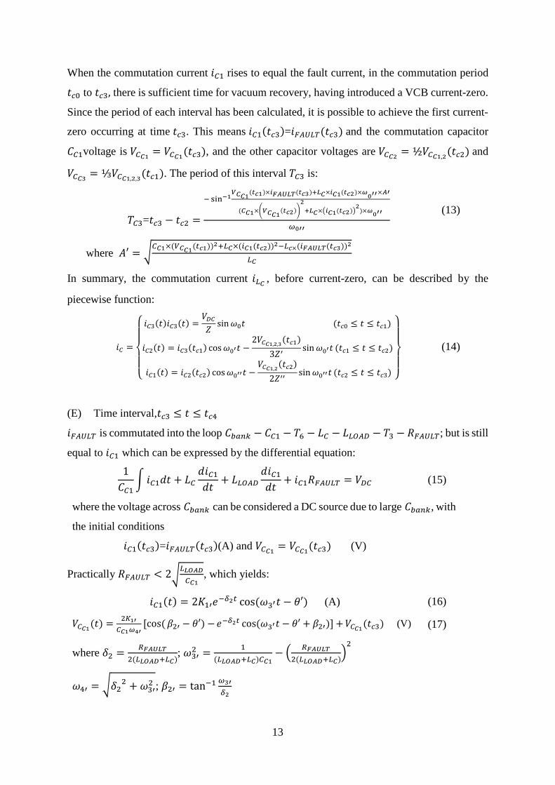
Fig. 4(a) shows the commutation capacitor voltage and current. The current 𝑑𝑑𝐶𝐶 through the
commutation capacitor equals the fault current 𝑑𝑑𝐹𝐹𝐿𝐿𝐹𝐹𝐿𝐿𝑇𝑇 . Due to the stored magnetic energy
transfer and the residual voltage of the commutation capacitor, there is an initial increase in 𝑑𝑑𝐶𝐶
after the current-zero. Since the solid-state switches offer uni-directional conduction, the
commutation capacitor should be fully charged and is kept unchanged when 𝑑𝑑𝐶𝐶 reduces to zero.
17
Fig. 4: Commutation capacitor voltage and current profiles. (a) The performance of commutation capacitor current and voltage after current-zero and (b) Maximum discharge time with two initial commutation capacitor voltages as a function of commutation capacitance. (𝐼𝐼𝐹𝐹𝐿𝐿𝐹𝐹𝐿𝐿𝑇𝑇 = 100A,𝑑𝑑𝐷𝐷𝐶𝐶 = 600V, 𝐿𝐿𝐶𝐶 = 49.4µH,𝐿𝐿𝐿𝐿𝐿𝐿𝐿𝐿𝐷𝐷 = 1.7mF,𝑅𝑅𝐹𝐹𝐿𝐿𝐹𝐹𝐿𝐿𝑇𝑇 = 6Ω)
The most significant design aspect is the period immediately following the current-zero in the
VCB. Thus it is convenience to specify the duration from the initial residual capacitor voltage
to when it retains zero charge. Due to the complexity of the commutation capacitor voltage
equation, it is difficult to directly define a time interval equation. Capacitor voltage 𝑑𝑑𝐶𝐶
approaches zero when 𝑑𝑑𝐶𝐶 increases to its maximum. The approximate equation for the time
interval after current-zero is obtained by equating the current differential equation (24) with
zero, which gives:
𝑇𝑇𝐶𝐶 = −ln(−𝑒𝑒
2𝑗𝑗𝜃𝜃(𝛿𝛿2 + 𝜔𝜔3𝑗𝑗)𝛿𝛿2 − 𝜔𝜔3𝑗𝑗
)𝑗𝑗
2𝜔𝜔3 (25)
where 𝑗𝑗 = √−1
Hence
𝑇𝑇𝐶𝐶4=𝑑𝑑𝑐𝑐4 − 𝑑𝑑𝑐𝑐3 = −ln(−𝑒𝑒
2𝑗𝑗𝜃𝜃′(𝛿𝛿2+𝜔𝜔3′𝑗𝑗)𝛿𝛿2−𝜔𝜔3′𝑗𝑗
)𝑗𝑗
2𝜔𝜔3′ (26)
𝑇𝑇𝐶𝐶5=𝑑𝑑𝑐𝑐5 − 𝑑𝑑𝑐𝑐4 = −ln(−𝑒𝑒
2𝑗𝑗𝜃𝜃′′(𝛿𝛿2+𝜔𝜔3′′𝑗𝑗)𝛿𝛿2−𝜔𝜔3′′𝑗𝑗
)𝑗𝑗
2𝜔𝜔3′′ (27)
The plots in Fig. 4(b) are for equation (26) with two initial residual capacitor voltages. The
time interval increases with an increase in commutation capacitance and its initial residual
voltage.
Since these time intervals are based on maximum discharge ability for each commutation
capacitor voltage, it ensures 𝑑𝑑𝑉𝑉𝐶𝐶𝑉𝑉 produces second current-zero if interruption failure occurs at
the first current-zero.
Cc
Tim
e (s
)
(a) (b)
0
0iC
VCc
t (s)
Curr
ent (
A)
Vol
tage
(V)
Initial increase
Full charged
100
50
0 9 10 5−× 1.8 10 4−× 2.7 10 4−× 3.6 10 4−× 4.5 10 4−× 0 9 10 5−× 1.8 10 4−× 2.7 10 4−× 3.6 10 4−× 4.5 10 4−×0
8 10 5−×
1.6 10 4−×
2.4 10 4−×
3.2 10 4−×
4 10 4−×
Vc=-150Vc=-300
VV
VCc=-150VCc=-300
iC=0
18
There are six sequential time intervals, TC1-TC2-TC3-TC4-TC5-TC6, in the operation cycle of the
cascaded commutation circuit. TC3 and TC4 are from the same signal impulse, which triggers
switches T3-T4-T5 in the correct sequence. The first three time intervals TC1-TC2-TC3 involve the
𝑑𝑑𝑑𝑑/𝑑𝑑𝑑𝑑 reduction while the remainder are for improving the re-applied 𝑑𝑑𝑑𝑑𝑉𝑉𝐶𝐶𝑉𝑉 𝑑𝑑𝑑𝑑⁄ . Since TC3 and
TC4 are derived from the same signal, they can be considered ‘joined’, linking the reducing
current before current-zero and the increasing voltage after current-zero. They maintain
continuity during commutation. This means, commutation current 𝑑𝑑𝐿𝐿𝐶𝐶 has to rise to 𝑑𝑑𝐹𝐹𝐿𝐿𝐹𝐹𝐿𝐿𝑇𝑇 in
first two time intervals. Assuming the fault current is commutated into the VCB at the end of
the first interval; the interruption process can be expressed as follows:
𝑇𝑇𝐶𝐶10=𝑑𝑑𝑐𝑐1 − 𝑑𝑑𝑐𝑐0 =−sin−1𝑖𝑖𝐹𝐹𝐴𝐴𝐹𝐹𝐿𝐿𝐹𝐹
(𝑡𝑡𝑐𝑐1)𝑍𝑍𝑉𝑉𝐷𝐷𝐶𝐶
𝜔𝜔0 (28)
where 𝜔𝜔0 = 1 𝐿𝐿𝐶𝐶𝐶𝐶𝐶𝐶1,2,3⁄ (rad/s)
If 𝑑𝑑𝐹𝐹𝐿𝐿𝐹𝐹𝐿𝐿𝑇𝑇 is commutated at 𝑑𝑑𝑐𝑐2 , equation (9) for describing the time interval 𝑇𝑇𝐶𝐶2 can be
rewritten as:
𝑇𝑇𝐶𝐶20=𝑑𝑑𝑐𝑐2 − 𝑑𝑑𝑐𝑐1 =
−sin−1𝑉𝑉𝐶𝐶𝐶𝐶1,2(𝑡𝑡𝑐𝑐1)×𝑖𝑖𝐹𝐹𝐴𝐴𝐹𝐹𝐿𝐿𝐹𝐹(𝑡𝑡𝑐𝑐2)+𝐿𝐿𝐶𝐶×𝑖𝑖𝐹𝐹𝐴𝐴𝐹𝐹𝐿𝐿𝐹𝐹(𝑡𝑡𝑐𝑐2)×𝜔𝜔0′×𝐴𝐴
(𝐶𝐶𝐶𝐶1,2×𝑉𝑉𝐶𝐶𝐶𝐶1,2(𝑡𝑡𝑐𝑐1)
2+𝐿𝐿𝐶𝐶×𝑖𝑖𝐹𝐹𝐴𝐴𝐹𝐹𝐿𝐿𝐹𝐹(𝑡𝑡𝑐𝑐2)
2)×𝜔𝜔0′
𝜔𝜔0′
(29)
where 𝐴𝐴 = 𝐶𝐶𝐶𝐶1,2×(𝑉𝑉𝐶𝐶𝐶𝐶1,2(𝑡𝑡𝑐𝑐1))2+𝐿𝐿𝐶𝐶×(𝑖𝑖𝐹𝐹𝐴𝐴𝐹𝐹𝐿𝐿𝐹𝐹(𝑡𝑡𝑐𝑐2))2−𝐿𝐿𝑐𝑐×(𝑖𝑖𝐹𝐹𝐴𝐴𝐹𝐹𝐿𝐿𝐹𝐹(𝑡𝑡𝑐𝑐2))2
𝐿𝐿𝐶𝐶
𝑑𝑑𝐶𝐶𝐶𝐶1,2(𝑑𝑑𝑐𝑐1) = −⅔𝑑𝑑𝐷𝐷𝐶𝐶 cos𝜔𝜔0𝑑𝑑𝑐𝑐1
𝑑𝑑𝐹𝐹𝐿𝐿𝐹𝐹𝐿𝐿𝑇𝑇(𝑑𝑑𝑐𝑐1) = 𝑑𝑑𝐹𝐹𝐿𝐿𝐹𝐹𝐿𝐿𝑇𝑇(𝑑𝑑𝑐𝑐2) due to large time constant of the fault path. Now considering 𝑑𝑑𝑐𝑐0 as
a start point, 𝑇𝑇𝐶𝐶1 = 𝑑𝑑𝑐𝑐1 − 𝑑𝑑𝑐𝑐0 = 𝑑𝑑, the total duration can be defined as:
𝑇𝑇𝐶𝐶1,2=𝑑𝑑𝑐𝑐2 − 𝑑𝑑𝑐𝑐0 = 𝑇𝑇𝐶𝐶2 + 𝑇𝑇𝐶𝐶1 = 𝑇𝑇𝐶𝐶20 + 𝑑𝑑 (30)
To specify the time interval becomes a trade-off between 𝑇𝑇𝐶𝐶1 and 𝑇𝑇𝐶𝐶2.
The graphs in Fig. 5 represent equations (29) to (31) for the different conditions but at a fixed
600V DC source. Based on the fixed fault current of 100A and commutation parameters
including 𝐿𝐿𝐶𝐶 = 49.4µH and 𝐶𝐶𝐶𝐶1 = 40µF , Fig. 5(a) compares the total duration 𝑇𝑇𝐶𝐶1,2 and
second time interval 𝑇𝑇𝐶𝐶20, as well as the first current-zero time 𝑇𝑇𝐶𝐶10 of the test circuit. It reveals
how the 𝑑𝑑𝑑𝑑/𝑑𝑑𝑑𝑑 is reduced by the cascaded circuit. The horizontal axis represents the first time
interval, 𝑇𝑇𝐶𝐶1 = 𝑑𝑑𝑐𝑐1 − 𝑑𝑑𝑐𝑐0 = 𝑑𝑑 . The second time interval reduces as the first time interval
increases, meaning a longer first time interval will result in less time for the second interval,
thereby reducing𝑇𝑇𝐶𝐶1,2. To maximise the cascaded circuit commutation time, the second time
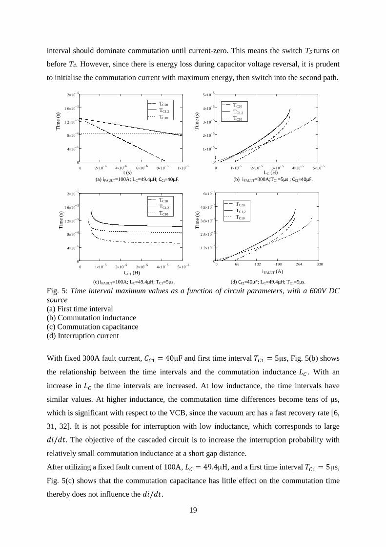
19
interval should dominate commutation until current-zero. This means the switch T5 turns on
before T4. However, since there is energy loss during capacitor voltage reversal, it is prudent
to initialise the commutation current with maximum energy, then switch into the second path.
Fig. 5: Time interval maximum values as a function of circuit parameters, with a 600V DC source (a) First time interval (b) Commutation inductance (c) Commutation capacitance (d) Interruption current
With fixed 300A fault current, 𝐶𝐶𝐶𝐶1 = 40µF and first time interval 𝑇𝑇𝐶𝐶1 = 5µs, Fig. 5(b) shows
the relationship between the time intervals and the commutation inductance 𝐿𝐿𝐶𝐶 . With an
increase in 𝐿𝐿𝐶𝐶 the time intervals are increased. At low inductance, the time intervals have
similar values. At higher inductance, the commutation time differences become tens of μs,
which is significant with respect to the VCB, since the vacuum arc has a fast recovery rate [6,
31, 32]. It is not possible for interruption with low inductance, which corresponds to large
𝑑𝑑𝑑𝑑/𝑑𝑑𝑑𝑑. The objective of the cascaded circuit is to increase the interruption probability with
relatively small commutation inductance at a short gap distance.
After utilizing a fixed fault current of 100A, 𝐿𝐿𝐶𝐶 = 49.4µH, and a first time interval 𝑇𝑇𝐶𝐶1 = 5µs,
Fig. 5(c) shows that the commutation capacitance has little effect on the commutation time
thereby does not influence the 𝑑𝑑𝑑𝑑/𝑑𝑑𝑑𝑑.
TC20
TC1,2
TC10
0 2 10 6−× 4 10 6−× 6 10 6−× 8 10 6−× 1 10 5−×0
4 10 6−×
8 10 6−×
1.2 10 5−×
1.6 10 5−×
2 10 5−×
TC20
TC1,2
TC10
t (s)
Tim
e (s
)
Tim
e (s
)
Tim
e (s
)
LC (H)
CC1 (H) iFAULT (A)
Tim
e (s
)TC20
TC1,2
TC10
TC20
TC1,2
TC10
(a) (b)
(c) (d)
iFAULT=100A; LC=49.4μH; CC1=40μF. iFAULT=300A;TC1=5μs ; CC1=40μF.
0 1 10 5−× 2 10 5−× 3 10 5−× 4 10 5−× 5 10 5−×0
1 10 5−×
2 10 5−×
3 10 5−×
4 10 5−×
5 10 5−×
0 1 10 5−× 2 10 5−× 3 10 5−× 4 10 5−× 5 10 5−×0
4 10 6−×
8 10 6−×
1.2 10 5−×
1.6 10 5−×
2 10 5−×
iFAULT=100A; LC=49.4μH; TC1=5μs. CC1=40μF; LC=49.4μH; TC1=5μs.
0 66 132 198 264 3300
1.2 10 5−×
2.4 10 5−×
3.6 10 5−×
4.8 10 5−×
6 10 5−×
20
With a first time interval of 5μs and commutation parameters 𝐿𝐿𝐶𝐶 = 49.4µH and 𝐶𝐶𝐶𝐶1 = 40µF,
the relationship between the time intervals and the fault current is shown in Fig. 5(d). The time
intervals display an ever-increasing trend with an increase in the fault current; but are similar
at low 𝑑𝑑𝐹𝐹𝐿𝐿𝐹𝐹𝐿𝐿𝑇𝑇.
In summary, although there are six time intervals, TC1-TC2-TC3-TC4-TC5-TC6, in the cascaded
circuit, only TC1-TC2-TC3-TC4-TC5 need to be specified because TC6 is a long signal impulse
lasting until the end of the interruption. TC3-TC4 are from same signal, thus there are only four
signals to be processed. In order to specify these time intervals, the first two intervals should
be defined first by utilizing equations (29) and (30). The remaining two can be obtained from
equation (26) in terms of different initial conditions.
21
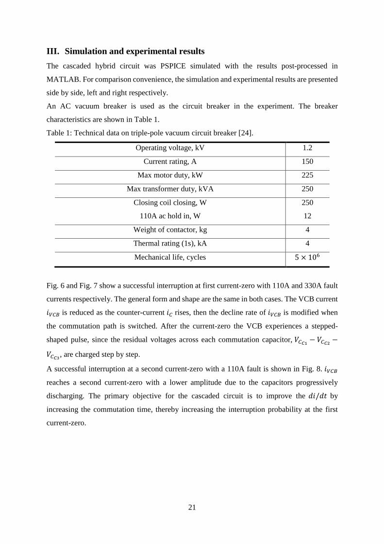
III. Simulation and experimental results The cascaded hybrid circuit was PSPICE simulated with the results post-processed in
MATLAB. For comparison convenience, the simulation and experimental results are presented
side by side, left and right respectively.
An AC vacuum breaker is used as the circuit breaker in the experiment. The breaker
characteristics are shown in Table 1.
Table 1: Technical data on triple-pole vacuum circuit breaker [24].
Operating voltage, kV 1.2
Current rating, A 150
Max motor duty, kW 225
Max transformer duty, kVA 250
Closing coil closing, W
110A ac hold in, W
250
12
Weight of contactor, kg 4
Thermal rating (1s), kA 4
Mechanical life, cycles 5 × 10⁶
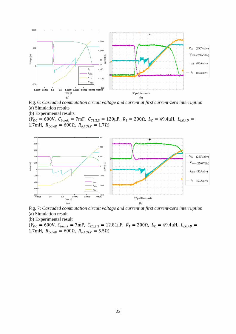
Fig. 6 and Fig. 7 show a successful interruption at first current-zero with 110A and 330A fault
currents respectively. The general form and shape are the same in both cases. The VCB current
𝑑𝑑𝑉𝑉𝐶𝐶𝑉𝑉 is reduced as the counter-current 𝑑𝑑𝐶𝐶 rises, then the decline rate of 𝑑𝑑𝑉𝑉𝐶𝐶𝑉𝑉 is modified when
the commutation path is switched. After the current-zero the VCB experiences a stepped-
shaped pulse, since the residual voltages across each commutation capacitor, 𝑑𝑑𝐶𝐶𝐶𝐶1 − 𝑑𝑑𝐶𝐶𝐶𝐶2 −
𝑑𝑑𝐶𝐶𝐶𝐶3, are charged step by step.
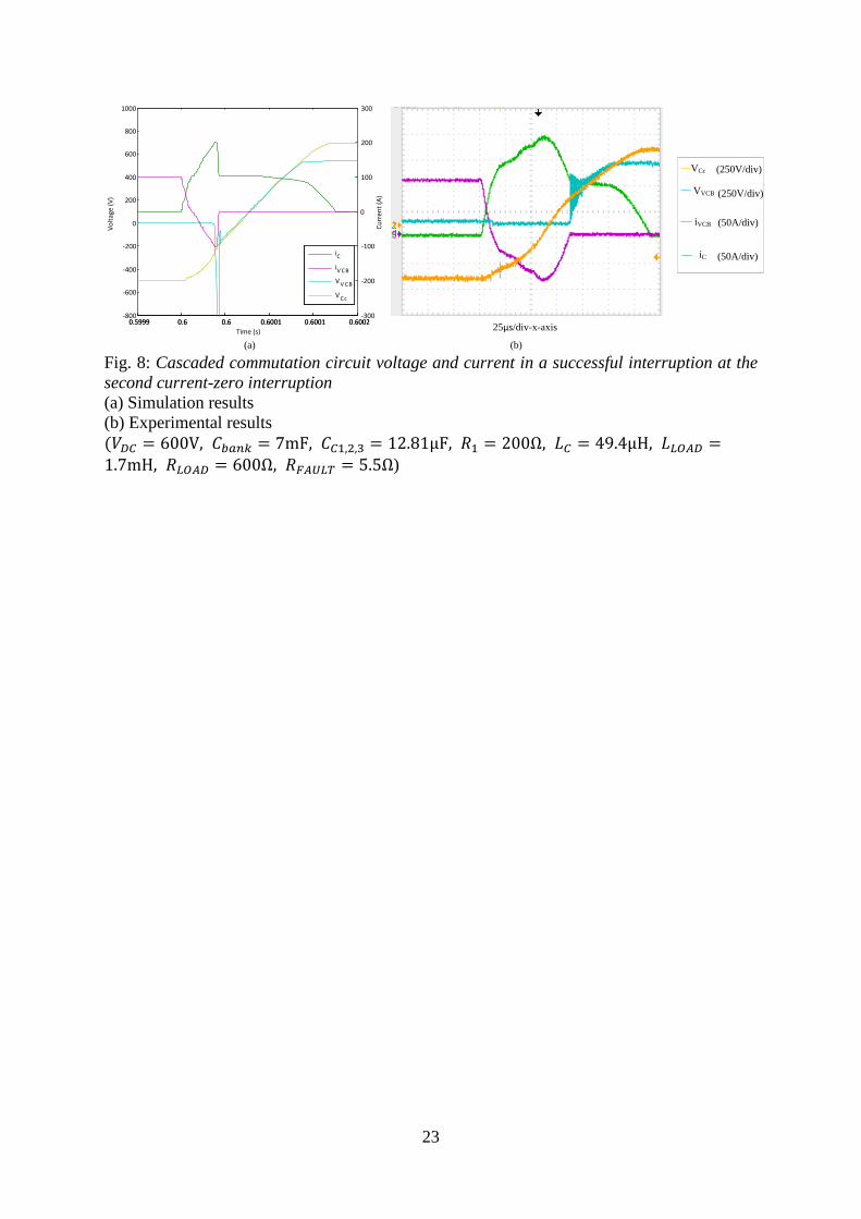
A successful interruption at a second current-zero with a 110A fault is shown in Fig. 8. 𝑑𝑑𝑉𝑉𝐶𝐶𝑉𝑉
reaches a second current-zero with a lower amplitude due to the capacitors progressively
discharging. The primary objective for the cascaded circuit is to improve the 𝑑𝑑𝑑𝑑/𝑑𝑑𝑑𝑑 by
increasing the commutation time, thereby increasing the interruption probability at the first
current-zero.
22
Fig. 6: Cascaded commutation circuit voltage and current at first current-zero interruption (a) Simulation results (b) Experimental results (𝑑𝑑𝐷𝐷𝐶𝐶 = 600V, 𝐶𝐶𝑏𝑏𝑏𝑏𝑏𝑏𝑏𝑏 = 7mF, 𝐶𝐶𝐶𝐶1,2,3 = 120µF, 𝑅𝑅1 = 200Ω, 𝐿𝐿𝐶𝐶 = 49.4µH, 𝐿𝐿𝐿𝐿𝐿𝐿𝐿𝐿𝐷𝐷 =1.7mH, 𝑅𝑅𝐿𝐿𝐿𝐿𝐿𝐿𝐷𝐷 = 600Ω, 𝑅𝑅𝐹𝐹𝐿𝐿𝐹𝐹𝐿𝐿𝑇𝑇 = 1.7Ω)
Fig. 7: Cascaded commutation circuit voltage and current at first current-zero interruption (a) Simulation result (b) Experimental result (𝑑𝑑𝐷𝐷𝐶𝐶 = 600V, 𝐶𝐶𝑏𝑏𝑏𝑏𝑏𝑏𝑏𝑏 = 7mF, 𝐶𝐶𝐶𝐶1,2,3 = 12.81µF, 𝑅𝑅1 = 200Ω, 𝐿𝐿𝐶𝐶 = 49.4µH, 𝐿𝐿𝐿𝐿𝐿𝐿𝐿𝐿𝐷𝐷 =1.7mH, 𝑅𝑅𝐿𝐿𝐿𝐿𝐿𝐿𝐷𝐷 = 600Ω, 𝑅𝑅𝐹𝐹𝐿𝐿𝐹𝐹𝐿𝐿𝑇𝑇 = 5.5Ω)
0.5999 0.5999 0.6 0.6 0.6000 0.6001 0.6002 0.6003 0.6003
-500
0
500
1000
Time (s)
Volta
ge (V
)
0.5999 0.5999 0.6 0.6 0.6000 0.6001 0.6002 0.6003 0.6003-300
-180
-60
60
180
300
Curr
ent (
A)
iCiV C B
V Cc
V V C B
50μs/div-x-axis
(250V/div)VCc
(250V/div)VVCB
(80A/div)iVCB
iC (80A/div)
0
(a) (b)
0.5999 0.6 0.6 0.6001 0.6001 0.6002-800
-600
-400
-200
0
200
400
600
800
1000
Time (s)
Volta
ge (V
)
0.5999 0.6 0.6 0.6001 0.6001 0.6002-300
-200
-100
0
100
200
300
Curr
ent (
A)
iCiV CB
VV CB
VCc
(250V/div)VCc
(250V/div)VVCB
(50A/div)iVCB
iC (50A/div)
25μs/div-x-axis
(a) (b)
23
Fig. 8: Cascaded commutation circuit voltage and current in a successful interruption at the second current-zero interruption (a) Simulation results (b) Experimental results (𝑑𝑑𝐷𝐷𝐶𝐶 = 600V, 𝐶𝐶𝑏𝑏𝑏𝑏𝑏𝑏𝑏𝑏 = 7mF, 𝐶𝐶𝐶𝐶1,2,3 = 12.81µF, 𝑅𝑅1 = 200Ω, 𝐿𝐿𝐶𝐶 = 49.4µH, 𝐿𝐿𝐿𝐿𝐿𝐿𝐿𝐿𝐷𝐷 =1.7mH, 𝑅𝑅𝐿𝐿𝐿𝐿𝐿𝐿𝐷𝐷 = 600Ω, 𝑅𝑅𝐹𝐹𝐿𝐿𝐹𝐹𝐿𝐿𝑇𝑇 = 5.5Ω)
0.5999 0.6 0.6 0.6001 0.6001 0.6002-800
-600
-400
-200
0
200
400
600
800
1000
Time (s)
Volta
ge (V
)
0.5999 0.6 0.6 0.6001 0.6001 0.6002-300
-200
-100
0
100
200
300
Curr
ent (
A)
iCiV CB
VV CB
VCc
(250V/div)VCc
(250V/div)VVCB
(50A/div)iVCB
iC (50A/div)
25μs/div-x-axis
(a) (b)

24
IV. CONCLUSION This paper proposed a cascaded commutation circuit, without snubber circuits, inspiration by
a saturable reactor which slowed the di/dt prior to current-zero and then produced a low voltage
amplitude pulse. The validity of cascaded commutation principle was confirmed by simulation
and experimentally. The experimental results are conducted at a lower power level in order to
validate the commutation circuit performance.
Successful fault current interruption at the first and second current-zeros is achieved with
decreased 𝑑𝑑𝑑𝑑/𝑑𝑑𝑑𝑑 and 𝑑𝑑𝑑𝑑𝑉𝑉𝐶𝐶𝑉𝑉 𝑑𝑑𝑑𝑑⁄ .The proposed cascaded commutation circuitry shows only
three cascaded voltage stages but this can be increased, depending on the voltage resolution of
the dVVCB/dt and the DC system voltage. T2 and T4 in Fig. 1 can be combined into a single back-
to-back configuration, saving two diodes, but is not shown in this paper to give circuit analysis
simplicity. The proposed circuit architecture consist of a single IGBT device in each cascaded
voltage stage, which its voltage rating is associated with its capacitor voltage level. Lower
IGBT voltage devices can be used to reduce the power losses during the commutation process
but will result in more cascaded voltage stages. However, the voltage resolution of dVVCB/dt is
increased.
Conventional series connected capacitors required shunted resistors for voltage balancing and
discharge of the capacitors energy when the power system is disconnected. However, when
this technique is employed in the proposed circuit, the capacitors voltage need to be trickled
charge by T1 to maintain its DC voltages as DC fault does not occur frequently. This approach
is currently employed in the proposed circuit. The alternative approach in the proposed
technique is not using shunt resistor but overrate the capacitor voltage rating according to the
capacitor tolerances. This eliminates the trickle charge process but required auxiliary circuit to
discharge the capacitor energy when repair or maintenance work to the system is necessary.
Timing control on the respective gate signals in the three level cascaded voltage stages are
accomplished by a mid-range 16-bit micro-controller (dsPIC30F2020), utilizing only 60% of
the controller capability. The controller algorithm is not presented as the primary focus is to
demonstrate the proposed commutation circuit performance. Isolation of the IGBT gate drives
between each voltage stages can be accomplished by utilizing fibre-optic technologies, greatly
enhancing the reliability of the cascaded commutation circuit.
The proposed technique is analysed and demonstrated under uni-directional DC current flow
system. However, its feasibility in bidirectional DC current flow system is possible by
replacing the diodes (T2, T4, T5 and T6) in the cascaded commutation circuit with IGBTs. This
25
allows bidirectional current flow in the commutation circuit. Alternative control mechanism is
needed for bidirectional DC current fault interruption. Detailed operational structure of the
proposed technique for bidirectional current interruption is not presented in this paper.
Total failure in operation of the devices during fault condition can result DC arcing in the
mechanical DC breaker. Failure Mode Evaluation Analysis (FMEA) on the proposed
commutation circuit is not presented in this paper and is proposed for future works.
V. ACKNOWLEDGEMENT The authors gratefully acknowledge the support of EPSRC grant EP/K035096/1: Underpinning
Power Electronics 2012 – Converters theme.
26
REFERENCE [1] C. Meyer, S. Schroder, and R. W. D. Doncker, "Solid-state circuit breakers and current
limiters for medium-voltage systems having distributed power systems," IEEE Transactions on Power Electronics, vol. 19, pp. 1333-1340, 2004.
[2] R. Sirsi, S. Prasad, A. Sonawane, and A. Lokhande, "Efficiency comparison of AC distribution system and DC distribution system in microgrid," in 2016 International Conference on Energy Efficient Technologies for Sustainability (ICEETS), 2016, pp. 325-329.
[3] R. Mehl and P. Meckler, "Comparison of advantages and disadvantages of electronic and mechanical Protection systems for higher Voltage DC 400 V," in Telecommunications Energy Conference 'Smart Power and Efficiency' (INTELEC), Proceedings of 2013 35th International, 2013, pp. 1-7.
[4] M. Corti, E. Tironi, and G. Ubezio, "DC Networks Including Multiport DC/DC Converters: Fault Analysis," IEEE Transactions on Industry Applications, vol. 52, pp. 3655-3662, 2016.
[5] J. C. Das, "Arc-Flash Hazard Calculations in LV and MV DC Systems Part—II: Analysis," Industry Applications, IEEE Transactions on, vol. 50, pp. 1698-1705, 2014.
[6] M. Walter and C. Franck, "Improved Method for Direct Black-Box Arc Parameter Determination and Model Validation," Power Delivery, IEEE Transactions on, vol. 29, pp. 580-588, 2014.
[7] M. B. Schulman and P. G. Slade, "Sequential modes of drawn vacuum arcs between butt contacts for currents in the 1 kA to 16 kA range," Components, Packaging, and Manufacturing Technology, Part A, IEEE Transactions on, vol. 18, pp. 417-422, 1995.
[8] R. Zhigang, M. Ruiguang, S. Hao, N. Jiaqi, C. Zhexin, and N. Chunping, "Experimental investigation of arc characteristics in medium-voltage DC circuit breaker," in TENCON 2013 - 2013 IEEE Region 10 Conference (31194), 2013, pp. 1-4.
[9] H. Y. Elzagzoug, J. W. Spencer, and A. G. Deakin, "DC Current Limitation Principle Using a Helical Arc Arrangement," Power Delivery, IEEE Transactions on, vol. 30, pp. 122-128, 2015.
[10] P. Chang, I. Husain, A. Huang, B. Lequesne, and R. Briggs, "A fast mechanical switch for medium voltage hybrid DC and AC circuit breakers," in Energy Conversion Congress and Exposition (ECCE), 2015 IEEE, 2015, pp. 5211-5218.
[11] J. Jadidian, "A Compact Design for High Voltage Direct Current Circuit Breaker," IEEE Transactions on Plasma Science, vol. 37, pp. 1084-1091, 2009.
[12] K. A. Corzine and R. W. Ashton, "A New Z-Source DC Circuit Breaker," Power Electronics, IEEE Transactions on, vol. 27, pp. 2796-2804, 2012.
[13] M. Kempkes, I. Roth, and M. Gaudreau, "Solid-state circuit breakers for Medium Voltage DC power," in Electric Ship Technologies Symposium (ESTS), 2011 IEEE, 2011, pp. 254-257.
[14] S. Juvekar, B. Compton, and S. Bhattacharya, "A fast acting DC solid state fault isolation device (FID) with Si and SiC devices for MVDC distribution system," in Energy Conversion Congress and Exposition (ECCE), 2012 IEEE, 2012, pp. 2005-2010.
[15] Z. J. Shen, G. Sabui, M. Zhenyu, and S. Zhikang, "Wide-Bandgap Solid-State Circuit Breakers for DC Power Systems: Device and Circuit Considerations," Electron Devices, IEEE Transactions on, vol. 62, pp. 294-300, 2015.
[16] J. Millan, P. Godignon, X. Perpina, A. Perez-Tomas, and J. Rebollo, "A Survey of Wide Bandgap Power Semiconductor Devices," Power Electronics, IEEE Transactions on, vol. 29, pp. 2155-2163, 2014.
27
[17] T. C. Lim, B. W. Williams, S. J. Finney, and P. R. Palmer, "Series-Connected IGBTs Using Active Voltage Control Technique," Power Electronics, IEEE Transactions on, vol. 28, pp. 4083-4103, 2013.
[18] P. Chang, A. Q. Huang, and S. Xiaoqing, "Current commutation in a medium voltage hybrid DC circuit breaker using 15 kV vacuum switch and SiC devices," in Applied Power Electronics Conference and Exposition (APEC), 2015 IEEE, 2015, pp. 2244-2250.
[19] W. Yifei, R. Mingzhe, W. Yi, Y. Fei, L. Mei, and L. Yang, "Development of a new topology of dc hybrid circuit breaker," in Electric Power Equipment - Switching Technology (ICEPE-ST), 2013 2nd International Conference on, 2013, pp. 1-4.
[20] L. Luhui, Z. Jinwu, W. Chen, J. Zhuangxian, W. Jin, and C. Bo, "A Hybrid DC Vacuum Circuit Breaker for Medium Voltage: Principle and First Measurements," Power Delivery, IEEE Transactions on, vol. 30, pp. 2096-2101, 2015.
[21] Y. W. Yifei Wu, Mingzhe Rong, Fei Yang, Chunping Niu, Mei Li, Yang Hu "Research on a novel two-stage direct current hybrid circuit breaker," AIP Review of Scientific Instruments, vol. 85, 2014.
[22] Y. Shan, T. C. Lim, B. W. Williams, and S. J. Finney, "Successful fault current interruption on DC circuit breaker," IET Power Electronics, vol. 9, pp. 207-218, 2016.
[23] ABB, "The Hybrid HVDC Breaker An innovation breakthrough enabling reliable HVDC grids."
[24] K. Shenai, "Power Electronic Module: Enabling the 21st-century energy economy," Power Electronics Magazine, IEEE, vol. 1, pp. 27-32, 2014.
[25] J. Dries, "SiC Research and Development at United Silicon Carbide Inc.?Looking Beyond 650?1,200 V Diodes and Transistors [Happenings]," Power Electronics Magazine, IEEE, vol. 2, pp. 12-15, 2015.
[26] J. F. Donlon, E. R. Motto, E. Wiesner, E. Thal, K. Hatori, Y. Sakai, S. Kitamura, T. Motomiya, K. Ota, Y. Kitajima, S. Iura, H. Yamaguchi, and K. Kurachi, "The next generation 6.5kV IGBT," in Energy Conversion Congress and Exposition (ECCE), 2014 IEEE, 2014, pp. 2897-2900.
[27] L. Zhenxian, N. Puqi, and F. Wang, "Development of Advanced All-SiC Power Modules," Power Electronics, IEEE Transactions on, vol. 29, pp. 2289-2295, 2014.
[28] S. Madhusoodhanan, K. Hatua, S. Bhattacharya, S. Leslie, R. Sei-Hyung, M. Das, A. Agarwal, and D. Grider, "Comparison study of 12kV n-type SiC IGBT with 10kV SiC MOSFET and 6.5kV Si IGBT based on 3L-NPC VSC applications," in Energy Conversion Congress and Exposition (ECCE), 2012 IEEE, 2012, pp. 310-317.
[29] C. Meyer, M. Kowal, and R. W. De Doncker, "Circuit breaker concepts for future high-power DC-applications," in Industry Applications Conference, 2005. Fourtieth IAS Annual Meeting. Conference Record of the 2005, 2005, pp. 860-866 Vol. 2.
[30] Y. Shan, "Direct Current Hybrid Vacuum Breaker," PhD thesis, University of Strathclyde, 2014.
[31] M. M. Walter and C. M. Franck, "Optimal Test Current Shape for Accurate Arc Characteristic Determination," Power Delivery, IEEE Transactions on, vol. 29, pp. 1798-1805, 2014.
[32] G. A. Farrall, "Recovery of Dielectric Strength after Current Interruption in Vacuum," Plasma Science, IEEE Transactions on, vol. 6, pp. 360-369, 1978.