cadence virtuoso schematic composer introduction contentsvlsi/ece559_fall09/lab/559tut_1... ·...
TRANSCRIPT
1
ECE 559 Lab Tutorial 1
Cadence Virtuoso Schematic Composer Introduction
Contents 1 Introduction ............................................................................................................................. 2
2 Getting Started ......................................................................................................................... 2
3 Online Documentation ............................................................................................................. 2
4 Virtuoso Schematic Composer Basics ..................................................................................... 3
4.1 Launch Virtuoso Schematic Composer ............................................................................ 34.2 Setup User Preferences..................................................................................................... 44.3 Library Manager ............................................................................................................... 54.4 Creating a New Library .................................................................................................... 64.5 Creating a New Cellview ................................................................................................. 6
5 Drawing a Schematic for a CMOS Inverter ............................................................................ 7
5.1 Adding Instances .............................................................................................................. 75.2 Editing Instance Properties............................................................................................. 105.3 Displaying Instance Properties ....................................................................................... 105.4 Deleting Instances .......................................................................................................... 115.5 Adding Pins .................................................................................................................... 115.6 Adding Wires ................................................................................................................. 125.7 Naming Nets ................................................................................................................... 12
6 Checking and Saving Your Schematic .................................................................................. 13
7 Creating and Editing a Symbol for Your Schematic ............................................................. 14
8 Creating Parameterized Inverter ............................................................................................ 16
8.1 Creating Schematic ........................................................................................................ 168.2 Creating Symbol ............................................................................................................. 168.3 Adding CDF parameter .................................................................................................. 17
9 Create a New Schematic to be Simulated .............................................................................. 18
9.1 InverterTest Schematic ................................................................................................... 189.2 Hierarchy Editing ........................................................................................................... 20
10 Printing from Cadence ........................................................................................................... 22
2
1 I n t r o d u c t i o n
The purpose of the first lab tutorial is to help you become familiar with the schematic editor, Virtuoso Schematic Composer. You will create a schematic and a symbol for a static CMOS inverter. After completion of this tutorial, you should be able to:
- Insert instances into your design - Connect instances together using wires - Change instance properties - Name nets - Add pins to your design - Create and edit a symbol cellview - Check and save your design - Do a hierarchical design using cells that you have designed - Use buses and tap wires from buses. 2
G e t t i n g S t a r t e d• Log into your workstation. You should already have access to the workstations
using your login and password that are provided by TA. You should not use your career login and password as in general you would not have access to the tools that you need. If you have problems logging in, please consult your TA.
• Open a terminal window.
• Enter source /package/eda/bin/vlsi_setup in any UNIX terminal window and press enter. Note that you only need to do this the first time you start using Cadence.
• The above command copies the files cds.lib, .cdsinit, and .cdsenv files. These files contain the path of the library files and the environment settings. It also copies the .cshrc file which contains the commands used to source the toolset.
3
O n l i n e D o c u m e n t a t i o nNote that this tutorial and the following series cover only the very fundamental concepts of creating CMOS schematics, symbols and layouts, simulating circuits,

3
performing layout verification and parasitic extraction from layout using Cadence. Please refer to the online documentation should you require additional information.
• To access the online documentation, type ic5141doc in a terminal window.
• In the online documentation, more detailed information can be found under the
Virtuoso Composer product. Under Manuals, there are the Virtuoso Schematic Editor Tutorial and the Virtuoso Schematic Editor User Guide that you may find helpful. 4
V i r t u o s o S c h e m a t i c C o m p o s e r B a s i c sThe Virtuoso Schematic Composer is used to create the schematic of your design. In the schematic, it will contain devices (transistors) connected together with nets (wire connections).
4 . 1 L a u n c h V i r t u o s o S c h e m a t i c C o m p o s e r• Enter grid icfb in a terminal window command prompt. A window should
appear with the title icfb at the top. This window is known as the Command Interpreter Window (CIW). It is the main control window for the schematic composer software. Various properties can also be changed in this window. Other commands that can be used to launch the CIW, depending on the tools that you require, include: icde – includes the basic IC design entry package icds – includes design and simulation tools icms – a larger set of tools for mixed signal design msfb – supports an IC design flow without place and route icfb – complete front-to-back design set
4
• The CIW displays a running history of the commands that you execute and their results. It also shows status and error messages from the schematic composer software.
• When commands are run, the CIW will display prompts for action.
• Please note that typing icfb will also open the CIW window but that will only open files in read-only formats.
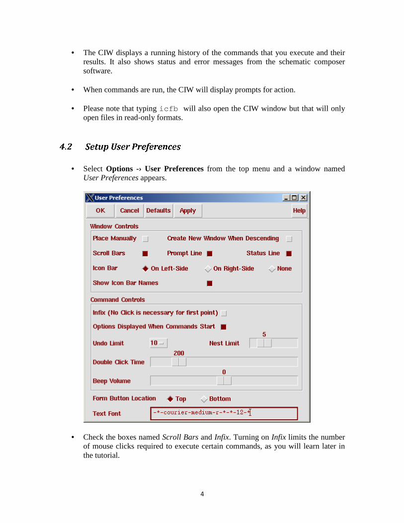
4 . 2 S e t u p U s e r P r e f e r e n c e s• Select Options -› User Preferences from the top menu and a window named
User Preferences appears.
• Check the boxes named Scroll Bars and Infix. Turning on Infix limits the number of mouse clicks required to execute certain commands, as you will learn later in the tutorial.

5
• Set the Undo Limit to 10. Click OK to exit. 4 . 3 L i b r a r y M a n a g e r
The Library Manager allows you to manage (create, copy, move, delete) libraries. It is recommended that all changes in the libraries be done here to preserve the integrity of all the files associated with your design. • To run Library Manager, click on Tools -› Library Manager.
• Cadence uses the term library to mean both reference libraries, which contain defined components for a specific technology, and design libraries, in which you create your own designs. The designs are called cells.
• Each cell can have multiple representations, such as a symbol or a schematic. These representations are called cellviews.
• There should be several libraries already present in the Library column. Click on any of the libraries. It will list some cells in the Cell column that belongs to this library. You should see a library called NCSU_Analog_Parts. This will probably be the most often used library for this course, as you will find out later on.
6
• The cellviews associated with the cell will appear in the View column if you click on any of the cells listed.
• The pathnames of these libraries are defined in the cds.lib file. The paths can be altered manually with a text editor if required.
• It is also possible to open designs from the library manager. To do this, either right click on the cellview and select Open from the menu that appears or simply double click on the cellview name. 4 . 4
C r e a t i n g a N e w L i b r a r y• To create a new library, click on File -› New -› Library (you can do this in either
the icfb window or the Library Manager). A new window appears and type tutorial in the Name. If you see a library named tutorial already there, you don’t need to create it.
• Under Technology Library, click on Attach to existing techfile. The technology file (techfile) stores all the instances, process and rules files required for schematic and layout design. Select TSMC 0.30u CMOS025 as your techfile and click OK . 4 . 5
C r e a t i n g a N e w C e l l v i e w• To create a new cell view, click on File -› New -› Cellview (you can do this in
either the icfb window or the Library Manager). A window appears and select tutorial for the Library Name field, and type in inverter for the Cell Name. The View Name should be schematic and the Tool field should be Composer-Schematic. Click OK when done.
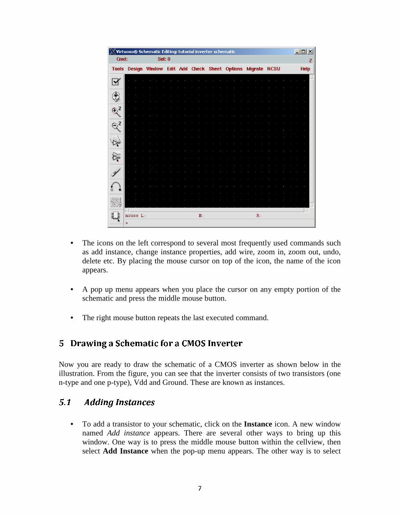
• A new window named Virtuoso Schematic Editing: tutorial inverter schematic should appear. This is the schematic window or cellview. Note that the last parts of the window name correspond to the library (tutorial) and the cellview (inverter) that you are currently working on.
• Take a look at the command menu on top and the icons on the left. Clicking on the top (drop down) menu will reveal more command options. If there is an arrow to the right of the command option in the drop down menu, it means that there are more options under it.
• Next to certain command options, there are some letters next to it. These are bindkeys (or more commonly known as hot-keys) that invoke the command using simple key presses. They will become handy when you get more familiar with the schematic editor and the bindkeys.
7
• The icons on the left correspond to several most frequently used commands such as add instance, change instance properties, add wire, zoom in, zoom out, undo, delete etc. By placing the mouse cursor on top of the icon, the name of the icon appears.
• A pop up menu appears when you place the cursor on any empty portion of the schematic and press the middle mouse button.
• The right mouse button repeats the last executed command. 5 D r a w i n g a S c h e m a t i c f o r a C M O S I n v e r t e r
Now you are ready to draw the schematic of a CMOS inverter as shown below in the illustration. From the figure, you can see that the inverter consists of two transistors (one n-type and one p-type), Vdd and Ground. These are known as instances. 5 . 1
A d d i n g I n s t a n c e s• To add a transistor to your schematic, click on the Instance icon. A new window
named Add instance appears. There are several other ways to bring up this window. One way is to press the middle mouse button within the cellview, then select Add Instance when the pop-up menu appears. The other way is to select

8
Add -› Instance from the top menu. The last but probably the most convenient way is to use hot-key (in this case, press ‘i’ on the keyboard).
• In this new window, click on the Browse button to browse available libraries. Another new window named Component Browser.
• In the new window, select the NCSU_Analog_Parts library, then select N_Transistors and then nmos4. Now move the mouse cursor back to the schematic window and you will find a symbol representing an n-type transistor attached to the cursor.
• You can rotate or flip the instance (sideways or upside down) by clicking the Rotate, Sideways and Upside Down buttons in the window before placement.

9
• If you have accidentally chosen the wrong instance, press the Esc key or click the Cancel button on the Add Instance window.
• Move the cursor to a desired location on the schematic window and click the mouse button to put the transistor in place.
• After the placement of the n-type transistor, it will continue to prompt you to add another instance (same instance by default). This will allow you to place multiple instances onto your cellview. Return to the Component Browser and under the same library, select P_Transistors and then pmos4. Place a p-type transistor in the schematic window.
• Continue to add the remaining instances (Vdd and Gnd) into your cellview from the NCSU_Analog_Parts library under Supply_Net.
• Press the Esc key to stop adding more instances.
• You can simply click and drag the instance around to re-position them on your cellview.
1 0
5 . 2
E d i t i n g I n s t a n c e P r o p e r t i e s• To modify the properties of an instance, such as the width and length of the n-type
transistor, select the n-type transistor and click the Property icon on the left or selecting Edit -› Properties -› Objects from the drop down menu (hot-key is ‘q’).
• A new window named Edit Object Properties appears. The Library Name, Cell Name and View Name are displayed near the middle section. Ensure that these values correspond to the right instance before modifying the properties.
• For the Instance Name field, it can be changed to any value for easy identification between instances.
• For the CDF Parameters change the Width to 0.45u and the Length to 0.3u (u represents micrometers and n represents nanometers). Use the Tab key or mouse to move between fields and do not press the Enter key unless you are done.
• To change the properties for another instance, click on the instance and the Edit Object Properties window will be updated to the new instance.
• As an exercise, change the properties of the p-type transistor such that the width is 0.9u and the length is 0.3u.
• After done editing, click OK or press Enter to quit.
• Note that other instance properties can be edited in the same manner. 5 . 3 D i s p l a y i n g I n s t a n c e P r o p e r t i e s• It is possible to make the instance properties that you specified above visible in
the schematic. This provides a quick view to the property values that you entered for each instance.
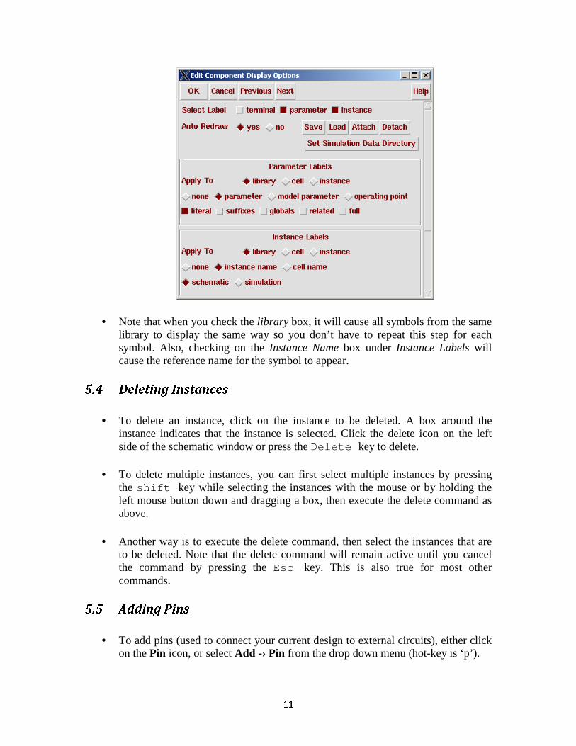
• To change the display options, click on Edit -› Component Display. A new window will appear.
• In the schematic, click on a component that you want to display values for.
• In the Component Display window, check the boxes as indicated in the figure below.
1 1
• Note that when you check the library box, it will cause all symbols from the same library to display the same way so you don’t have to repeat this step for each symbol. Also, checking on the Instance Name box under Instance Labels will cause the reference name for the symbol to appear. 5 . 4
D e l e t i n g I n s t a n c e s• To delete an instance, click on the instance to be deleted. A box around the
instance indicates that the instance is selected. Click the delete icon on the left side of the schematic window or press the Delete key to delete.
• To delete multiple instances, you can first select multiple instances by pressing the shift key while selecting the instances with the mouse or by holding the left mouse button down and dragging a box, then execute the delete command as above.
• Another way is to execute the delete command, then select the instances that are to be deleted. Note that the delete command will remain active until you cancel the command by pressing the Esc key. This is also true for most other commands. 5 . 5
A d d i n g P i n s• To add pins (used to connect your current design to external circuits), either click
on the Pin icon, or select Add -› Pin from the drop down menu (hot-key is ‘p’).
1 2
• A new window named Add Pin appears.
o Type In for the Pin Names field. o Select input for the Direction tab. o Leave other settings at their default state.
• Move the mouse cursor back to the schematic window and you will find a symbol
representing a pin attached to the cursor, similar to the placing of an instance.
• You can rotate or flip the symbol (sideways or upside down) by clicking the Rotate, Sideways and Upside Down buttons in the window before placement.
• As an exercise, add an output pin named Out. The Direction tab should be set to output this time. 5 . 6
A d d i n g W i r e s• To add wires to connect the instances together, click on the Wire (narrow) icon on
the left. Alternatively, click the middle mouse button within the cellview and select Wire (narrow) in the pop up. You might have noticed that there is a similar icon named Wire (wide). It is used to create buses.
• A new window named Add Wire appears. Leave the Draw Mode as route unless you absolutely need to draw non-rectilinear wires.
• Click on the wire starting point (for example, at the red boxes indicating an instance pin). Move the mouse cursor and click again for each wire segment.
• You might notice that as you move the mouse cursor, a small diamond shape appears over the connection object closest to the pointer. To end the wire, press s to snap to the nearest object that shows a diamond shape. Another way is to click a schematic pin, an instance pin, or another wire or double-click on a new wire endpoint.
• Finish up the schematic by connecting the instances together with wires.
• You should now have a schematic similar to the one in the diagram (schematic of CMOS inverter). 5 . 7
N a m i n g N e t s
• You might have noticed that in the schematic, the input pin is not connected to the schematic. By naming the net (or wire), it is possible to indicate that there is an
1 3
electrical connection between other nets or pins. This could help in reducing the amount of wire cluttering that makes the schematic hard to read.
• To name a net, select Add -› Wire Name from the drop down menu or select Add Name from the pop up menu. A new window named Add Wire Name appears. Type in In for the Names field and move the mouse cursor to the net that is to be named In.
• It is possible to add several names to different nets at one time. To do this, simply type the names separated by a space in the Names field and the names will be added in order when you click on the various nets. 6
C h e c k i n g a n d S a v i n g Y o u r S c h e m a t i cOnce you think that your schematic is complete, you will need to run a check on it. This check only checks for very rudimentary problems (such as unconnected pins or dangling wires) and for many more subtle or obscure problems that may cause trouble later on in programs that try to use your schematic.
• To check your schematic, click on the Check and Save icon. The results of the check are displayed in the CIW. If everything goes well, you should see a message in the CIW: Schematic check completed with no errors. “tutorial schematic inverter“ saved.
• As an exercise, delete a wire segment from your schematic and do a check. A window named Schematic Check will “appear indicating the number of errors and warnings found. Click Close.
• In the cellview, flashing markers highlight the areas that are causing the errors or warnings.
• To understand the cause of errors, select the drop down menu item Check -› Find Marker . A new window appears showing the list of errors and warnings.
• Clicking on a particular error and warning from the list will highlight the markers that correspond to that particular error or warning highlighted on the schematic. Click Delete to remove the marker from the cellview.
• There might be situations, for example, where you do not need to use a certain pin on an instance and would just want to leave it “floating”. The checker will indicate a warning that the pin is floating. To ignore the warning and to prevent it from appearing repeatedly, select the warning from the list and click Ignore. That
1 4
particular warning will not appear in the next check. To make the warning reappear, click Restore All in the same window.
• Fix the schematic, do a check and save it. 7 C r e a t i n g a n d E d i t i n g a S y m b o l f o r Y o u r S c h e m a t i c
At this point, you should have a schematic “view” of a CMOS inverter “cell” that passes the check without errors. You will now generate a symbol “view” for the inverter “cell”.
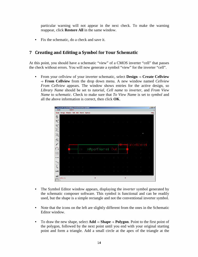
• From your cellview of your inverter schematic, select Design -› Create Cellview -› From Cellview from the drop down menu. A new window named Cellview From Cellview appears. The window shows entries for the active design, so Library Name should be set to tutorial, Cell name to inverter, and From View Name to schematic. Check to make sure that To View Name is set to symbol and all the above information is correct, then click OK .
• The Symbol Editor window appears, displaying the inverter symbol generated by the schematic composer software. This symbol is functional and can be readily used, but the shape is a simple rectangle and not the conventional inverter symbol.
• Note that the icons on the left are slightly different from the ones in the Schematic Editor window.
• To draw the new shape, select Add -› Shape -› Polygon. Point to the first point of the polygon, followed by the next point until you end with your original starting point and form a triangle. Add a small circle at the apex of the triangle at the

1 5
output end by selecting Add -› Shape -› Circle. Point and click to define the center of the circle and move to size the circle by moving the mouse.
• Carefully delete the inner box. Do not delete the outside box that runs through the pin squares.
• Select the top and bottom sides of the outside box and move them out to the points on the triangle (click and drag), so that the entire triangle is inside the box. This box determines the boundaries of the symbol (i.e., determines what area you click on the schematic to select the symbol)
• The final result should look like this:
• Check and save the symbol by using the Design -› Check and Save command from the drop down menu.
• If you take a look at the inverter cell in the tutorial library, you can see that it has now a schematic cellview and a symbol cellview.
• Close the Symbol Editor.
Now you have completed a discrete CMOS inverter design, with its own symbol, and the instance parameters as specified. The next step is to perform a simulation on the inverter to verify that it works and to evaluate its performance.

1 6
8 C r e a t i n g P a r a m e t e r i z e d I n v e r t e r
In the previous example, we created inverter schematic and symbol with fixed sizes (wp/lp = 600n/240n, wn/ln=300n/240n). What if you need another inverter with different sizes? Of course, you can create new inverter with different sizes but it’ll be easier to manage your project if you have a generalized inverter cell that you can specify the sizes in the higher level design. In this section, you will generate an inverter cell and symbol with the sizes parameterized. 8 . 1
C r e a t i n g S c h e m a t i cCreating a parameterized cell view is basically the same as the previous example except property setting.
• Create a new cellview
o Library : tutorial o Cell name : inverterp o View name : schematic o Tool : Composer-schematic
• Draw an inverter schematic (The width and length of transistors will be set at the
next step).
• In the property window of pfet (click pfet and use short cut key ‘q’), set width and length as follows
o width : pPar(“wp”) o length: pPar(“lp”)
• In the property window of nfet (click nfet and use short cut key ‘q’), set width and
length as follows
o width : pPar(“wn”) o length: pPar(“ln”)
• Check and Save the schematic 8 . 2 C r e a t i n g S y m b o l• Create a symbol as explained in section 7.
• To add NLPlabel, select Add -› Label and set the options as shown in the following picture.

1 7
• Repeat adding NLPLabel for nfet with the Label field ‘[@wn:%:][@ln:/%:]’.
• Check and Save the symbol.
• The final picture should look like as below figure.
8 . 3 A d d i n g C D F p a r a m e t e r• In the CIW, select Tools -› CDF -› Edit…

1 8
• Set CDF Type to base.
• Library Name should be set to tutorial, Cell name to inverterp (use browse button to select the library and cell name).
• Click Add button and Add CDF Parameter window will pop up if the parameters do not exist, otherwise select edit and select the parameter you would like to modify.
• Set paramType to float, storeDefault to yes, name to wp, prompt to wp and defValue to the default value you want.
• Repeat adding CDF parameters for lp, wn and ln.
• Now the parameterized inverter is ready to be used. 9 C r e a t e a N e w S c h e m a t i c t o b e s i m u l a t e d9 . 1
I n v e r t e r T e s t S c h e m a t i c• Under the same library (tutorial), create a new cellview named InverterTest.
• Use the Add Instance command to place your inverterp symbol in the cellview. It should be found under the tutorial library.

1 9
• If you open the property window of inverterp, you can find 4 CDF parameters. If the values for those parameters are not specified, set those parameters to wp/wn =900n/300n and wn/ln = 450n/300n.
• Use the Add Instance command to place two capacitors in the cellview from the NCSU_Analog_Parts library and give them a value of 10fF (when you type in the value in the property window, just type 10f).
• For this tutorial, we will create two bit wide buses for input, internal nodes and output. To add a bus, click the Wire (wide) icon. Draw the bus as you would draw any normal (narrow) wire.
• After creating the bus, the bus must be named. The same command to add wire names for narrow wires is used, however the syntax for naming the bus is slightly different.
• Bus names is in the form Name<a:b>, where a and b denotes the range of bits of the bus. Several two bit buses that will be created in this tutorial include In<0:1>, internal<0:1> and Out<0:1>.
• Similar to the previous tutorial, it is possible to add several names to different buses at one time. To do this, make sure the Bus Expansion button is off and simply type the names of the buses separated by a space in the Names field. The names will be added in order when you click on the various nets. As an exercise, create and name the buses similar to the ones in the final schematic.

2 0
• To draw or tap wires to and from the buses, draw wires from the buses and name them correspondingly to their bits. To name the individual bit lines, type in the bus name (e.g. In<0:1> or simply <0:1>) and turn on Bus Expansion in the Add Wire Name window. The Bus Expansion button is used to extract individual bit names from the bus. When you start placing the names on the wires, you will notice that the first name will be In<0> (or <0>), the next will be In<1> (or <1>), and so on.
• Setting the Placement button to multiple allows you to place an array of names, rather than one at a time.
• Complete, check and save the schematic so that it looks like the schematic shown below. Don’t forget to add the pins In<0:1> and Out<0:1>. Note that a Vdd instance is added (from the analogLib library) without any connection to the schematic. This is required to specify a global Vdd source for simulation. 9 . 2
H i e r a r c h y E d i t i n g• Suppose that you wanted to explore the schematic of the inverter. You can
traverse a design hierarchy to view or edit your inverter design by selecting the inverter, then select Design -› Hierarchy -› Descend Edit / Read (hotkeys are E/ e). Select schematic for the View Name. Click OK in the new window that appears.
• Now the cellview should change to the schematic view of your inverter, showing the transistors and the connections. If there are more levels to descend, you can continue to do so from here.

2 1

2 2
• Note that if you make and save any changes to the schematic in the lower levels, the whole design (top level) will be changed, including other designs that use this symbol.
• To return up one level or to the top view, use Design -› Hierarchy -› Return /Return To Top (hotkey is B). 1 0
P r i n t i n g f r o m C a d e n c e• To print out any type of cellview, select Design -› Plot -› Submit. In the new
window that appears, turn off the header option unless you want one. If you are creating a plot file for the color plotter, always turn this off.
• Click on the Plot Options box. In the Plot Options window, turn on the Center Plot option and choose an appropriate paper size:
For the laser printers, choose paper size A. Make sure the scale settings are set to fit within the paper size.
• Disable the mail log to option, or make sure that the username is one you want the mail sent to.
• You can print the generated plot file using
o lp -d printer-name filename
o p r i n t e r n a m e s M S E E 1 8 9 l a b : m s 1 8 9 c h 1 a n d m s 1 8 9 c h 2P O T R 3 6 0 l a b : p o t r 3 6 0 p 1 a n d p o t r 3 6 0 p 2