by rapid thermal processing - mdpi
TRANSCRIPT
crystals
Article
Imprinting the Polytype Structure of Silicon Carbideby Rapid Thermal Processing
Jörg Pezoldt 1,* and Volker Cimalla 2
1 Nanotechnology, Institute of Micro- and Nanoelectronics and Institute of Micro- and NanotechnologiesMacroNano, TU Ilmenau, P.O. Box 100565, 98684 Ilmenau, Germany
2 Fraunhofer IAF, Fraunhofer Institute for Applied Solid State Physics, Tullastraße 72, 79108 Freiburg,Germany; [email protected]
* Correspondence: [email protected]
Received: 30 April 2020; Accepted: 15 June 2020; Published: 18 June 2020�����������������
Abstract: Silicon carbide is a material with a multistable crystallographic structure, i.e., a polytypicmaterial. Different polytypes exhibit different band gaps and electronic properties with nearly identicalbasal plane lattice constants, making them interesting for heterostructures without concentrationgradients. The controlled formation of this heterostructure is still a challenge. The ability to adjust adefined temperature–time profile using rapid thermal processing was used to imprint the polytypetransitions by controlling the nucleation and structural evolution during the temperature ramp-upand the steady state. The influence of the linear heating-up rate velocity during ramp-up andsteady-state temperature on the crystal structure of amorphized ion-implanted silicon carbide layerswas studied and used to form heteropolytype structures. Integrating the structural selection propertiesof the non-isothermal annealing stage of the ion-implanted layers into an epitaxial growth processallows the imprinting of polytype patterns in epitaxial layers due to the structural replication of thepolytype pattern during epitaxial growth. The developed methodology paves the way for structuralselection and vertical and lateral polytype patterning. In rapid thermal chemical vapor deposition,the adjustment of the process parameters or the buffer layer allowed the nucleation and growth ofwurtzite silicon carbide.
Keywords: silicon carbide; rapid thermal processing; ion-implantation; epitaxy; CVD; sublimation;polytypism; phase transition; polytype transition; polytype control.
1. Introduction
Silicon carbide (SiC) is a wide band gap semiconductor material with properties making itunique for many applications. The wide band gap (ranging from 2.4 eV for the pure cubic structure(3C-SiC) to 3.4 eV for the pure wurtzite structure (2H-SiC)), good electron mobility, high saturationdrift velocity, high breakdown electric field, and high thermal conductivity catapulted the siliconcarbide into industrial mass production for the fabrication of competitive high-power, high-frequency,and high-temperature devices on large area substrates after a long and punishing developmentalperiod [1–9].
In processing technologies, the control of the thermal budget and the time–temperature profilesare used to imprint desired morphological signatures: For example, concentration gradients, surfaces,and interfaces as well as the crystal structure and defect densities in the constituting layers andareas. The techniques allowing control of the time-dependent temperature profile are rapid thermalprocessing technologies [10,11]. In the case of SiC, rapid thermal processing was mostly applied toimplant annealing [12–14], ohmic [15–17] and Schottky contact formation [16,18], carbonization ofsilicon substrates [19,20], SiC on Si epitaxial growth by rapid thermal chemical vapor deposition [21,22],
Crystals 2020, 10, 523; doi:10.3390/cryst10060523 www.mdpi.com/journal/crystals
Crystals 2020, 10, 523 2 of 21
as well as to liquid phase epitaxy of SiC on Si [23,24]. The investigations using the rapid thermalprocessing-based formation or growth of SiC were focused on pseudosubstrates for heteroepitaxialgrowth of SiC [21,25], III-nitrides [26], and ZnO [27], and the fabrication of heterobipolar deviceapplications [28,29]. Less attention was given to the possibility of the defined adjustment of a desiredtemperature–time profile, which allows control of the nucleation and structural evolution during theramp-up and steady state. This is important, especially in the case of materials with a multistablecrystal structure, which may occur in the form of different polymorphic or polytypic structures [30].
Polytypism is a special one-dimensional form of polymorphism and is a general behaviorof layered and close-packed structures, such as SiC. The structural reason is the possibility ofdifferent modes of stacking of one or more structural compatible units (structural modules).The phenomena of polytypism and polymorphism are substantially different from the physicalpoint of view. Polymorphic modifications of a given material are characterized by a stability rangein a phase diagram described by temperature, pressure, and composition. The transition from onepolymorph to another is a first-order phase transformation. On the contrary, except for very fewsmall period modifications, no such physical factors have been found to govern the formation ofpolytypes. Different polytypes of a given material can be formed under identical temperature, pressure,and concentration conditions. For polytypes, the “syntactic coalescence” of different polytypes, i.e.,the simultaneous coexistence of more than one polytype within a crystal or an epitaxial layer [30–37],or polytype inclusion formation after completing a technological process step [37–48] or deviceoperation [48–51] is a common effect. On the other hand, because of the different physical propertiesof the different polytypes, silicon carbide represents a family of semiconductor materials. They arenatural superlattices [52], except the short period 3C and 2H polytypes. The very low differencesof the lattice constants and thermal expansion coefficients of the different SiC polytypes in the basalplane allows, for example, the formation of chemically homogeneous heterojunctions by combiningthem into different types of heteropolytype structures [37,53–58]. The realization of them would allowthe formation of two-dimensional electron gases [59–62], heterojunction bipolar transistors [63,64],quantum wells [37,57,65–67], and heterocrystalline or heteropolytypic superlattices [68–73]. The mainchallenge to be solved on the way is the controlled design of a sharp interface between the constituentpolytypes in the heterostructure or the multilayers. This is a challenge up to now [37,57,74,75].These new types of structures offer, with their specific properties, new types of application fields.Therefore, the development of methods to control the formation or the growth of different polytypesaccording to a well-defined pattern is very intriguing for artificial crystal structure design anddevice applications.
In thin film-based technologies, such as microelectronics, there is a continuing demand for thedevelopment of new process techniques in order to reduce the number of steps required for devicefabrication. Selective deposition, i.e., local deposition of a desired phase on a desired substrate area,has recently attracted considerable attention [76]. In combination with the self-formation of planarand three-dimensional structures [77], it allows the engineering of materials and device structuresin two and three dimensions. Selective deposition is generally discussed in terms of area selectivity,with local deposition of one phase on desired areas of a substrate surface. However, materials with amultivariable structure offer additional possibilities for phase-selective deposition, transformation,or self-formation. Namely, the simultaneous selective deposition of two or more chemically identicalphases having different physical properties on different regions of a patterned substrate or, alternatively,their controlled transformation in desired areas into another crystal structure [37,53–58] could pave theway for the development of new structure and device formation technologies.
The aim of this paper was to present that rapid thermal processing (RTP) allows the developmentof an exact adjustable process cycle for structural control based on phase-selective formation of adesired polytype and the self-formation of the same polytype pattern in the grown epitaxial layer bystructural replication during epitaxial growth by sublimation. The process foundation is the interplaybetween ion implantation, annealing, and epitaxial growth during high-temperature RTP sublimation
Crystals 2020, 10, 523 3 of 21
growth. For structural control at low temperatures, the silicon to carbon ration and the replication ofthe polytype structure of the buffer layer formed on the silicon substrate are the key to nucleate andgrow an unusual silicon carbide polytype 2H.
2. Materials and Methods
For the experimental investigations, on-axis C-face (0001)-oriented 6H-SiC and 15R-SiC sublimationgrown single crystals were used. The C-face orientation was chosen, because the polytype growthtransition occurs at high temperatures at a lower growth rate than on the Si-face [55] and can beinduced easier and controlled on this polar face [33,55,78].
Processing and epitaxial growth was carried out with two different types of rapid thermalprocessing (RTP) equipment. The equipment, hereinafter referred to as high-temperature RTP,allows thermal processing at temperatures above the melting point of silicon. The processingtechnologies, referred to as low-temperature RTP, allows processing temperatures up to the meltingpoint of silicon. The first type is based on direct heating of graphite constructions, whereas thesecond type uses halogen lamps as heating elements, i.e., the standard RTP technology used in siliconmanufacturing technology.
Single-dose ion implantation of Al+ and Ar+ ions directly into C-face (0001)-oriented 6H-SiCsubstrates was carried out at energies of 80 keV to study the polytype phase formation’s dependenceon the ion implantation and annealing conditions as well as the impact of doping and non-dopingimpurities. The ion implantation doses were 5 × 10¹⁴, 1 × 10¹⁵, 5 × 10¹⁵. 1 × 10¹⁶, and 5 × 1016 cm−2.The annealing was carried out in a wide temperature range between 800 and 2200 K using a graphitedouble stripe heater in an argon-silicon atmosphere at 1 atm to suppress surface graphitization.The design of the graphite heater allows the adjustment of the linear heating-up ramp rate in a widerange. The annealing time was 10 s for annealing temperatures between 800 and 1400 K and 5 sfor higher annealing temperatures. To guarantee that the recrystallization occurred mainly at thesteady state of the temperature–time cycle, a high linear heating-up ramp rate of 700 K s−1 was chosen.For the investigation of the influence of the heating-up ramp rate on the polytype phase formation fora selected sample set (Al+, 1 × 10¹⁵ and 5 × 1015 cm−2, 80 kV), the heating-up ramp rates were chosenas 30, 120, 600, and 700 K s−1. The samples were annealed to 2200 K. The overall annealing procedurewas chosen so that the effective annealing time [79] was the same for all three linear heating-up ramps.
The influence of the structural modification of the ion-implanted substrates on the polytype phaseformation in the epitaxial layers grown on them was investigated using the modified sublimationsandwich method. The epitaxial growth was carried out on C-face (0001)-oriented 6H- and 15R-SiCsubstrates using a graphite crucible with a low thermal mass and resistive heating. The low thermalcapacity of the crucible allowed rapid heating-up, with ramp rates between 20 and 200 K s−1 and shortprocessing times. The crystal growth was carried out at 2100 K and a heating-up ramp rate of 30 K/sand process times of 30 s, 45 s, 1 min, and 2 min at the final temperature. The growth was carried outunder vacuum conditions. The base pressure was 10−6 Torr. The ion implantation was carried outdirectly in the substrates using Ar+ ions and an acceleration energy of 80 keV. The dose was set to3 × 1015 cm−2 to ensure complete amorphization of the implanted layer. To compare the growth onnon-treated and ion-implanted surface in the growth experiments, only one half of the crystal wasimplanted. For the demonstration of polytype pattering, local ion implantation through a shadowmask with openings of 50 × 50 µm2 was carried out at the same ion implantation conditions.
The low-temperature rapid thermal processing was carried out in a homemade rapid thermalprocessing reactor described in detail in [80]. For the rapid thermal chemical vapor deposition (RTCVD)on Si(111), SiH4–C3H8–H2 chemistry was used. The silicon wafer was cleaned using the standard RCA(Radio Corporation of America) cleaning procedure finished with an HF dip. After the transfer of theSi(111) samples into the rapid thermal processing reactor, they were in situ annealed at 1273 K for60 s in a hydrogen atmosphere. The hydrogen flow was set to 1000 sccm. Prior to the chemical vapordeposition of SiC, a carbonization step was carried out to form a 3C-SiC(111) buffer layer using 0.15 %
Crystals 2020, 10, 523 4 of 21
C3H8 in 1000 sccm H2. The substrate temperature for this process step was 1520 K at a linear heating-upramp rate of 50 K s−1. The chosen process conditions for the carbonization cause the formation ofsingle crystalline 3C-SiC(111) with a thickness of approximately 3 nm [20,22,81]. For the subsequentRTCVD of SiC, the flow rates of SiH4 and C3H8 were in the range of 0.5 and 50 sccm. The atomic ratioof silicon and carbon (Si/C) in the gas phase was varied in the range between 0.1 and 0.8. The flow rateof hydrogen was 1000 sccm. The heating ramp-up velocity was 50 K/s and for the steady state time,60 s was taken. The process temperature was varied in the range between 1370–1620 K.
The structure of the ion-implanted and annealed crystals as well as the grown layers wasinvestigated by reflection high energy electron diffraction (RHEED). The penetration depth of theelectrons strongly depends on the angle of incidence, the surface morphology, and the diffractioncondition and is in the range of 1 to 100 nm. The determination of the polytype structure was carried outby analyzing the diffraction spot geometry and symmetry using the methodology described in [82–85].
The growth rate was determined from the measured thickness of the epitaxial layers taking intoaccount the duration of the growth process. The thickness of the grown epitaxial layers was carriedout by step height measurements in the case of sublimation growth and by ellipsometry for RTCVDgrown films.
3. High-Temperature Rapid Thermal Processing of Ion-Implanted SiC
3.1. Phase Formation by Rapid Thermal Annealing of Ion Implanted Layers
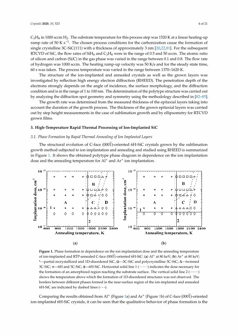
The structural evolution of C-face (0001)-oriented 6H-SiC crystals grown by the sublimationgrowth method subjected to ion implantation and annealing and studied using RHEED is summarizedin Figure 1. It shows the obtained polytype phase diagram in dependence on the ion implantationdose and the annealing temperature for Al+ and Ar+ ion implantation.
Crystals 2020, 10, x FOR PEER REVIEW 4 of 21
cause the formation of single crystalline 3C-SiC(111) with a thickness of approximately 3 nm [20,22,81]. For the subsequent RTCVD of SiC, the flow rates of SiH4 and C3H8 were in the range of 0.5 and 50 sccm. The atomic ratio of silicon and carbon (Si/C) in the gas phase was varied in the range between 0.1 and 0.8. The flow rate of hydrogen was 1000 sccm. The heating ramp-up velocity was 50 K/s and for the steady state time, 60 s was taken. The process temperature was varied in the range between 1370–1620 K.
The structure of the ion-implanted and annealed crystals as well as the grown layers was investigated by reflection high energy electron diffraction (RHEED). The penetration depth of the electrons strongly depends on the angle of incidence, the surface morphology, and the diffraction condition and is in the range of 1 to 100 nm. The determination of the polytype structure was carried out by analyzing the diffraction spot geometry and symmetry using the methodology described in [82–85].
The growth rate was determined from the measured thickness of the epitaxial layers taking into account the duration of the growth process. The thickness of the grown epitaxial layers was carried out by step height measurements in the case of sublimation growth and by ellipsometry for RTCVD grown films.
3. High-Temperature Rapid Thermal Processing of Ion-Implanted SiC
3.1. Phase Formation by Rapid Thermal Annealing of Ion Implanted Layers
The structural evolution of C-face (0001)-oriented 6H-SiC crystals grown by the sublimation growth method subjected to ion implantation and annealing and studied using RHEED is summarized in Figure 1. It shows the obtained polytype phase diagram in dependence on the ion implantation dose and the annealing temperature for Al+ and Ar+ ion implantation.
(a)
(b)
Figure 1. Phase formation in dependence on the ion implantation dose and the annealing temperature of ion-implanted and RTP-annealed C-face (0001)-oriented 6H-SiC: (a) Al+ at 80 keV; (b) Ar+ at 80 keV; * - partial recrystallized and 1D-disordered SiC, □ - 3C-SiC and polycrystalline 3C-SiC; Δ - twinned 3C-SiC; + - 6H and 3C-SiC; ◊ - 6H-SiC. Horizontal solid line 1 (______) indicates the dose necessary for the formation of an amorphized region reaching the substrate surface. The vertical solid line 2 (______) shows the temperature above which the formation of 1D-disordered structures was not observed. The borders between different phases formed in the near-surface region of the ion-implanted and annealed 6H-SiC are indicated by dashed lines (- - -).
Figure 1. Phase formation in dependence on the ion implantation dose and the annealing temperatureof ion-implanted and RTP-annealed C-face (0001)-oriented 6H-SiC: (a) Al+ at 80 keV; (b) Ar+ at 80 keV;*—partial recrystallized and 1D-disordered SiC, �—3C-SiC and polycrystalline 3C-SiC; ∆—twinned3C-SiC; +—6H and 3C-SiC; ♦—6H-SiC. Horizontal solid line 1 (______) indicates the dose necessary forthe formation of an amorphized region reaching the substrate surface. The vertical solid line 2 (______)shows the temperature above which the formation of 1D-disordered structures was not observed. Theborders between different phases formed in the near-surface region of the ion-implanted and annealed6H-SiC are indicated by dashed lines (- - -).
Comparing the results obtained from Al+ (Figure 1a) and Ar+ (Figure 1b) of C-face (0001)-orientedion-implanted 6H-SiC crystals, it can be seen that the qualitative behavior of phase formation is the
Crystals 2020, 10, 523 5 of 21
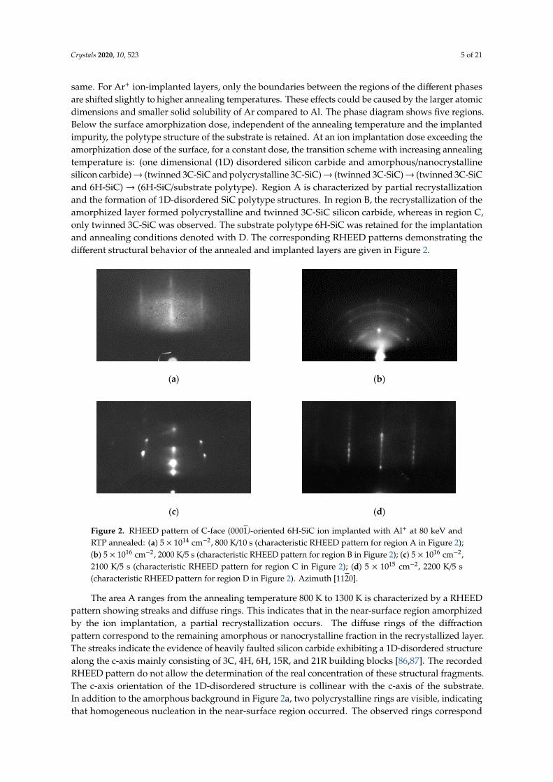
same. For Ar+ ion-implanted layers, only the boundaries between the regions of the different phasesare shifted slightly to higher annealing temperatures. These effects could be caused by the larger atomicdimensions and smaller solid solubility of Ar compared to Al. The phase diagram shows five regions.Below the surface amorphization dose, independent of the annealing temperature and the implantedimpurity, the polytype structure of the substrate is retained. At an ion implantation dose exceeding theamorphization dose of the surface, for a constant dose, the transition scheme with increasing annealingtemperature is: (one dimensional (1D) disordered silicon carbide and amorphous/nanocrystallinesilicon carbide)→ (twinned 3C-SiC and polycrystalline 3C-SiC)→ (twinned 3C-SiC)→ (twinned 3C-SiCand 6H-SiC)→ (6H-SiC/substrate polytype). Region A is characterized by partial recrystallizationand the formation of 1D-disordered SiC polytype structures. In region B, the recrystallization of theamorphized layer formed polycrystalline and twinned 3C-SiC silicon carbide, whereas in region C,only twinned 3C-SiC was observed. The substrate polytype 6H-SiC was retained for the implantationand annealing conditions denoted with D. The corresponding RHEED patterns demonstrating thedifferent structural behavior of the annealed and implanted layers are given in Figure 2.
Crystals 2020, 10, x FOR PEER REVIEW 5 of 21
Comparing the results obtained from Al+ (Figure 1a) and Ar+ (Figure 1b) of C-face (0001)-oriented ion-implanted 6H-SiC crystals, it can be seen that the qualitative behavior of phase formation is the same. For Ar+ ion-implanted layers, only the boundaries between the regions of the different phases are shifted slightly to higher annealing temperatures. These effects could be caused by the larger atomic dimensions and smaller solid solubility of Ar compared to Al. The phase diagram shows five regions. Below the surface amorphization dose, independent of the annealing temperature and the implanted impurity, the polytype structure of the substrate is retained. At an ion implantation dose exceeding the amorphization dose of the surface, for a constant dose, the transition scheme with increasing annealing temperature is: (one dimensional (1D) disordered silicon carbide and amorphous/nanocrystalline silicon carbide) → (twinned 3C-SiC and polycrystalline 3C-SiC) → (twinned 3C-SiC) → (twinned 3C-SiC and 6H-SiC) → (6H-SiC/substrate polytype). Region A is characterized by partial recrystallization and the formation of 1D-disordered SiC polytype structures. In region B, the recrystallization of the amorphized layer formed polycrystalline and twinned 3C-SiC silicon carbide, whereas in region C, only twinned 3C-SiC was observed. The substrate polytype 6H-SiC was retained for the implantation and annealing conditions denoted with D. The corresponding RHEED patterns demonstrating the different structural behavior of the annealed and implanted layers are given in Figure 2.
(a)
(b)
(c)
(d)
Figure 2. RHEED pattern of C-face (0001)-oriented 6H-SiC ion implanted with Al+ at 80 keV and RTP annealed: (a) 5 × 1014 cm−2, 800 K / 10 s (characteristic RHEED pattern for region A in Figure 2); (b) 5 × 1016 cm−2, 2000 K / 5 s (characteristic RHEED pattern for region B in Figure 2); (c) 5 × 1016 cm−2, 2100 K / 5 s (characteristic RHEED pattern for region C in Figure 2); (d) 5 × 1015 cm−2, 2200 K / 5 s (characteristic RHEED pattern for region D in Figure 2). Azimuth [1120].
The area A ranges from the annealing temperature 800 K to 1300 K is characterized by a RHEED pattern showing streaks and diffuse rings. This indicates that in the near-surface region amorphized by the ion implantation, a partial recrystallization occurs. The diffuse rings of the diffraction pattern correspond to the remaining amorphous or nanocrystalline fraction in the recrystallized layer. The streaks indicate the evidence of heavily faulted silicon carbide exhibiting a 1D-disordered structure along the c-axis mainly consisting of 3C, 4H, 6H, 15R, and 21R building blocks [86,87]. The recorded
Figure 2. RHEED pattern of C-face (0001)-oriented 6H-SiC ion implanted with Al+ at 80 keV andRTP annealed: (a) 5 × 1014 cm−2, 800 K/10 s (characteristic RHEED pattern for region A in Figure 2);(b) 5 × 1016 cm−2, 2000 K/5 s (characteristic RHEED pattern for region B in Figure 2); (c) 5 × 1016 cm−2,2100 K/5 s (characteristic RHEED pattern for region C in Figure 2); (d) 5 × 1015 cm−2, 2200 K/5 s(characteristic RHEED pattern for region D in Figure 2). Azimuth [1120].
The area A ranges from the annealing temperature 800 K to 1300 K is characterized by a RHEEDpattern showing streaks and diffuse rings. This indicates that in the near-surface region amorphizedby the ion implantation, a partial recrystallization occurs. The diffuse rings of the diffractionpattern correspond to the remaining amorphous or nanocrystalline fraction in the recrystallized layer.The streaks indicate the evidence of heavily faulted silicon carbide exhibiting a 1D-disordered structurealong the c-axis mainly consisting of 3C, 4H, 6H, 15R, and 21R building blocks [86,87]. The recordedRHEED pattern do not allow the determination of the real concentration of these structural fragments.The c-axis orientation of the 1D-disordered structure is collinear with the c-axis of the substrate.In addition to the amorphous background in Figure 2a, two polycrystalline rings are visible, indicatingthat homogeneous nucleation in the near-surface region occurred. The observed rings correspond
Crystals 2020, 10, 523 6 of 21
to homogeneous nucleated 3C-SiC frequently observed during the annealing of amorphous siliconcarbide layers [88–91]. With an increasing annealing temperature, the intensity of the polycrystallinerings and the streaks along the <h0l0> direction increases (not shown here). This indicates thatthe amorphous fraction of the implanted layer continuously decreases with an increasing annealingtemperature. The dimensions of the crystallites estimated from the full width of the half maximumfrom the diffraction rings were in the range of 2–7 nm. This crystallite size increases with the increasingannealing temperature.
The intermediate temperature range is divided into two different regions depending on theimplantation dose. They are denoted with B and C. For ion implantation doses equal or above5 × 1015 cm−2 (region B in Figure 1), only polycrystalline diffraction rings and diffraction spotscorresponding to twinned single crystalline 3C-SiC were observed on the RHEED pattern (Figure 2b).The twinned 3C would be formed during the epitaxial recrystallization of the amorphized SiC layerstarting at the amorphous–crystalline interface, whereas the polycrystalline fraction occurs due to thecompeting mechanism of solid phase epitaxial recrystallization, the homogenous nucleation and growth,which lead to the formation of polycrystalline layers due to the random nucleation orientation [92].Bohn et al. [93] observed the existence of a critical temperature for epitaxial recrystallization ofamorphized ion-implanted silicon carbide layers. Nevertheless, the existence of this mechanism is stillunder debate [92,94–97]. According to [93], the critical temperature for the epitaxial recrystallizationwas determined to be in the temperature range between 1670 and 1720 K. This critical temperaturedivides the region above the line 1 into two parts. At recrystallization temperatures below the criticaltemperature, the reason for the formation of the polycrystalline fraction could be the homogenousnucleation in the amorphous layer. For annealing temperatures above the critical temperature,the formation of the polycrystalline fraction is shifted to higher implantation doses and may be causedby impurity accommodation at the growth front, changing the crystallization mechanism in a similarway as the observations for Si revealed [98].
The region C in Figure 1 corresponds to the spotty RHEED pattern, shown in Figure 2c, indicatingthe formation of twinned 3C-SiC. In this region, polycrystalline diffraction features were not recorded.Therefore, at implantation doses between 1 × 10¹⁵ and 1 × 1016 cm−2 and annealing temperatures between1700 and 2000 K, the homogeneous nucleation of 3C-SiC can be suppressed. The necessary annealingtemperature is dose dependent (see Figure 2) and increases with an increasing ion implantation dose.The annealing temperature of region C exceeds the critical temperature of the epitaxial recrystallizationobtained in [93]. Therefore, it could be concluded that the 3C was formed during a solid phase epitaxialregrowth process, in wich the structural replication of the substrate polytype is blocked.
In the region D, characterized by annealing temperatures exceeding 2000 K, the polytype structureof the recrystallized layer resembles the polytype structure of the substrate (Figures 1 and 2d). It isnoticeable that higher implantation doses increase the annealing temperature necessary for therestoration of the substrate polytype structure. This might be caused by segregation effects and byhigher stresses induced by higher impurity concentrations. In an intermediate region between thephase regions C and D, the formation of two coexisting polytypes 3C and 6H is possible.
3.2. Influence of the Ramp Rate on the Structure of the Recrystallized Layer
The dependence of the crystal structure of the amorphized and recrystallized layers on theannealing temperature can be used to imprint desired 3C polytype patterns in α-SiC substrates.This was realized in [54]. This polytype patterning of the substrate can be applied to phase-selectivedeposition or the imprinting of a polytype pattern into a growing epitaxial layer. The precondition forstructural polytype imprinting is the well-known effect of the inheritance of the polytype structure fromthe substrate into the epitaxial layer [99–102]. For the design of a suitable process, the time–temperatureprofiles of the annealing and the epitaxial growth processes of SiC layers have to fulfill specificrequirements. Firstly, the polytype pattern formed in the substrate has to be retained during the
Crystals 2020, 10, 523 7 of 21
heating-up stage in the eptaxial growth process and, secondly, the polytype pattern has to be replicatedby the growing epitaxial layer.
Typically, the heating-up rates achieved in common growth equipment are slower than in the usedRTP graphite stripe heater system. For this reason, it is important to know how the phase formationduring recrystallization of the amorphized layer is affected by the heating rate. Furthermore, the structuralstability of the formed phase in the recrystallized layer has to be taken into account, because 3C-SiC isa metastable polytype and transforms into α-SiC at temperatures between 2000 and 2100 K [103–107].Therefore, an investigation is needed to understand the phase formation under non-isothermal conditions,i.e., the influence of the heating ramp on the phase formation in the recrystallizing layer as well as theeffect of the annealing time on the structural stability of the formed 3C-SiC has to be studied. The tuningof these two factors is important for the design of reliable process sequences for the realization of animprinted polytype pattern in the epitaxial layer by phase-selective growth.
For the investigation of these two process parameters, the following experiment was designed.A set of C-face (0001)-oriented 6H-SiC crystals ion-implanted with Al+ and doses 1 × 1015 cm−2
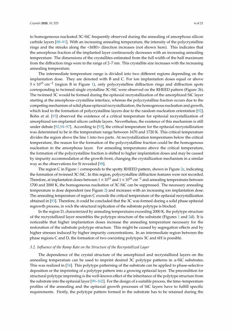
and 5 × 1015 cm−2 at 80 keV were annealed to 2200 K with linear heating-up ramp rates of 30, 120,and 600 K/s. The chosen annealing temperature leads to the formation of the substrate polytypeduring the isothermal annealing experiments (see region D in Figure 2a,b). Furthermore, the annealingprocedure was chosen so that the effective annealing time [79] was the same for all three heating-upramps. The RHEED patterns obtained from the samples are shown in Figure 3.
It is noticeable that the RHEED pattern obtained for slower heating ramps shows only the twinnedcubic structure (Figure 3a,b), whereas for the highest linear heating-up ramp rates of 600 and 700 K s−1,the polytype of the substrate was obtained (Figure 3c,f). A more detailed investigation of the RHEEDpattern ascertained that there are similarities in the fine structure of the RHEED pattern between therate-dependent annealing experiments, with a final annealing temperature of 2200 K and the RHEEDpattern obtained from the 6H-SiC crystals implanted with the same dose but annealed at differenttemperatures with a linear heating-up ramp rate of 700 K s−1. The results of the latter annealingconditions are given in Figure 3d–f. Figure 3a,d exhibit the same key diffraction features in the RHEEDpattern, namely, twinned 3C-SiC and polycrystalline 3C-SiC. The same holds for Figure 3b,e, in whichonly diffraction spots related to twinned 3C-SiC are visible. It is worth mentioning here that theRHEED pattern in Figure 3d,e were recorded from samples ion-implanted with the same dose butannealed with a linear heating-up ramp rate of 700 K s−1 to the final annealing temperatures of 1700and 1900 K, respectively. In Figure 3c,f, only diffraction spots stemming from 6H-SiC can be found.Therefore, linear heating-up ramp rates of 600 K s−1 are able to form the polytype structure of thesubstrate in the ion-implanted and amorphized SiC layer during the recrystallization process.
The recrystallization process of an amorphous layer can be described by the Avrami–Johnson–Mehl–Kolmogorov equation [108–111]:
dXdt
= [K(T) t]m(1−X), (1)
where X is the crystallized fraction in the amorphized layer, t is the annealing time, T is the annealingtemperature, m is the growth exponent, and K(T) is the rate constant. The rate constant is determined by:
K(T) = Ko exp(−
Ea
kT
), (2)
where Ko is a constant, k is the Boltzmann constant, and Ea is the overall activation energy. For the caseof a linear ramped profile (T = at + b) with a subsequent constant annealing temperature, the followingequations can be obtained.
Crystals 2020, 10, 523 8 of 21
Case 1: Linear ramping to a desired temperature (t < t1 = [Tmax − b]/a):
X(t) = 1− exp[−
∫ t
0(Ko t)m exp
(−
m Ea
k (at + b)
)dt
], (3)
Crystals 2020, 10, x FOR PEER REVIEW 7 of 21
time–temperature profiles of the annealing and the epitaxial growth processes of SiC layers have to fulfill specific requirements. Firstly, the polytype pattern formed in the substrate has to be retained during the heating-up stage in the eptaxial growth process and, secondly, the polytype pattern has to be replicated by the growing epitaxial layer.
For the investigation of these two process parameters, the following experiment was designed. A set of C-face (0001)-oriented 6H-SiC crystals ion-implanted with Al+ and doses 1 × 1015 cm−2 and 5 × 1015 cm−2 at 80 keV were annealed to 2200 K with linear heating-up ramp rates of 30, 120, and 600 K/s. The chosen annealing temperature leads to the formation of the substrate polytype during the isothermal annealing experiments (see region D in Figure 2a,b). Furthermore, the annealing procedure was chosen so that the effective annealing time [79] was the same for all three heating-up ramps. The RHEED patterns obtained from the samples are shown in Figure 3.
(a)
(d)
(b)
(e)
(c)
(f)
Figure 3. RHEED pattern of C-face (0001)-oriented 6H-SiC ion-implanted with Al+ with a dose of 5 × 1015 cm−2 at 80 keV and RTP annealed: (a) 30 K s−1 to 2200 K; (b) 120 K s−1 to 2200 K; (c) 600 K s−1 to 2200 K; (d) 700 K s−1 to 1700 K; (e) 700 K s−1 to 1900 K; (f) 700 K s−1 to 2200 K. Azimuth [1120].
It is noticeable that the RHEED pattern obtained for slower heating ramps shows only the twinned cubic structure (Figure 3a,b), whereas for the highest linear heating-up ramp rates of 600 and 700 K s−1, the polytype of the substrate was obtained (Figure 3 c,f). A more detailed investigation
Figure 3. RHEED pattern of C-face (0001)-oriented 6H-SiC ion-implanted with Al+ with a dose of 5 ×1015 cm−2 at 80 keV and RTP annealed: (a) 30 K s−1 to 2200 K; (b) 120 K s−1 to 2200 K; (c) 600 K s−1 to2200 K; (d) 700 K s−1 to 1700 K; (e) 700 K s−1 to 1900 K; (f) 700 K s−1 to 2200 K. Azimuth [1120].
Case 2: Linear ramping to a desired temperature with a steady state temperature plateau(t < t1 = Tmax − b)/a):
X(t) = 1− exp[−
∫ t
0
{(Ko t)m exp
(−
m Ea
k (at + b)
)−
Kmo
m + 1
(tm+1
− tm+11
)exp
(−
m Ea
k (at + b)
)Km
om + 1
}dt
]. (4)
The crystallization kinetics of deposited amorphous and amorphized by ion implantation siliconcarbide was studied in [112–117]. The activation energy of the recrystallization process scattersbetween 2.1 and 8.9 eV depending on the amorphous material and the substrate. For silicon andsilicon carbide substrates for deposited amorphous SiC [113,114] and amorphized by ion implantationSiC [116], the activation energy of the crystallization process was found to be in a narrow rangebetween 4.9 and 5.1 eV. The only exception is [117], where an activation energy of 2.1 eV was found
Crystals 2020, 10, 523 9 of 21
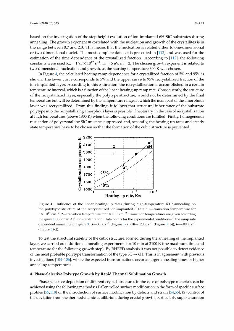
based on the investigation of the step height evolution of ion-implanted 6H-SiC substrates duringannealing. The growth exponent m correlated with the nucleation and growth of the crystallites is inthe range between 0.7 and 2.3. This means that the nucleation is related either to one-dimensionalor two-dimensional nuclei. The most complete data set is presented in [112] and was used for theestimation of the time dependence of the crystallized fraction. According to [112], the followingconstants were used Ko = 1.95 × 10¹² s−1, Ea = 5 eV, m = 2. The chosen growth exponent is related totwo-dimensional nucleation and growth, as the starting temperature 300 K was chosen.
In Figure 4, the calculated heating ramp dependence for a crystallized fraction of 5% and 95% isshown. The lower curve corresponds to 5% and the upper curve to 95% recrystallized fraction of theion-implanted layer. According to this estimation, the recrystallization is accomplished in a certaintemperature interval, which is a function of the linear heating-up ramp rate. Consequently, the structureof the recrystallized layer, especially the polytype structure, would not be determined by the finaltemperature but will be determined by the temperature range, at which the main part of the amorphouslayer was recrystallized. From this finding, it follows that structural inheritance of the substratepolytype into the recrystallizing amorphous layer is possible, if necessary, in the case of recrystallizationat high temperatures (above 1300 K) when the following conditions are fulfilled. Firstly, homogeneousnucleation of polycrystalline SiC must be suppressed and, secondly, the heating-up rates and steadystate temperature have to be chosen so that the formation of the cubic structure is prevented.
Crystals 2020, 10, x FOR PEER REVIEW 9 of 21
ion-implanted layer. According to this estimation, the recrystallization is accomplished in a certain temperature interval, which is a function of the linear heating-up ramp rate. Consequently, the structure of the recrystallized layer, especially the polytype structure, would not be determined by the final temperature but will be determined by the temperature range, at which the main part of the amorphous layer was recrystallized. From this finding, it follows that structural inheritance of the substrate polytype into the recrystallizing amorphous layer is possible, if necessary, in the case of recrystallization at high temperatures (above 1300 K) when the following conditions are fulfilled. Firstly, homogeneous nucleation of polycrystalline SiC must be suppressed and, secondly, the heating-up rates and steady state temperature have to be chosen so that the formation of the cubic structure is prevented.
Figure 4. Influence of the linear heating-up rates during high-temperature RTP annealing on the polytypic structure of the recrystallized ion-implanted 6H-SiC: 1 – transition temperature for 1 × 1015 cm−2; 2 - transition temperature for 5 × 1015 cm−2. Transition temperatures are given according to Figure 1 (a) for an Al+ ion-implantation. Data points for the experimental conditions of the ramp rate dependent annealing in Figure 3: ▲ – 30 K s−1 (Figure 3 (a)); ■ – 120 K s−1 (Figure 3 (b)); ♦ - 600 K s−1 (Figure 3 (c)).
To test the structural stability of the cubic structure, formed during the annealing of the implanted layer, we carried out additional annealing experiments for 10 min at 2100 K (the maximum time and temperature for the following growth step). By RHEED analysis it was not possible to detect evidence of the most probable polytype transformation of the type 3C → 6H. This is in agreement with previous investigations [104–106], where the expected transformations occur at larger annealing times or higher annealing temperatures.
4. Phase-Selective Polytype Growth by Rapid Thermal Sublimation Growth
Phase-selective deposition of different crystal structures in the case of polytype materials can be achieved using the following methods: (1) Controlled surface modification in the form of specific surface profiles [55,118] or the introduction of surface modification by defects and strain [54,55]; (2) control of the deviation from the thermodynamic equilibrium during crystal growth, particularly supersaturation and substrate temperature [55,119–121]; (3) change of the surface polarity [78]; (4) modification of the structural stability by the introduction of impurities in the growth zone [122–129]; (5) modification of the polytype structure of the substrate by stimulation of desired phase transitions [54,55,130]; or (6) deposition on isostructural materials [131].
Imprinting the polytype structure by phase-selective deposition of different polytypes on a patterned substrate by ion implantation and subsequent annealing belong to the fifth and sixth group of these process possibilities. The substrate temperature during sublimation growth occurs at temperatures in the range from 1900 to 2400 K. Therefore, reverse polytype transformations of the type 3C → α-SiC of the transformed areas of the patterned substrate are, in principle, possible. To
Figure 4. Influence of the linear heating-up rates during high-temperature RTP annealing onthe polytypic structure of the recrystallized ion-implanted 6H-SiC: 1—transition temperature for1 × 1015 cm−2; 2—transition temperature for 5× 1015 cm−2. Transition temperatures are given accordingto Figure 1 (a) for an Al+ ion-implantation. Data points for the experimental conditions of the ramp ratedependent annealing in Figure 3: N—30 K s−1 (Figure 3 (a)); �—120 K s−1 (Figure 3 (b)); �—600 K s−1
(Figure 3 (c)).
To test the structural stability of the cubic structure, formed during the annealing of the implantedlayer, we carried out additional annealing experiments for 10 min at 2100 K (the maximum time andtemperature for the following growth step). By RHEED analysis it was not possible to detect evidenceof the most probable polytype transformation of the type 3C→ 6H. This is in agreement with previousinvestigations [104–106], where the expected transformations occur at larger annealing times or higherannealing temperatures.
4. Phase-Selective Polytype Growth by Rapid Thermal Sublimation Growth
Phase-selective deposition of different crystal structures in the case of polytype materials can beachieved using the following methods: (1) Controlled surface modification in the form of specific surfaceprofiles [55,118] or the introduction of surface modification by defects and strain [54,55]; (2) control ofthe deviation from the thermodynamic equilibrium during crystal growth, particularly supersaturation
Crystals 2020, 10, 523 10 of 21
and substrate temperature [55,119–121]; (3) change of the surface polarity [78]; (4) modification of thestructural stability by the introduction of impurities in the growth zone [122–129]; (5) modificationof the polytype structure of the substrate by stimulation of desired phase transitions [54,55,130];or (6) deposition on isostructural materials [131].
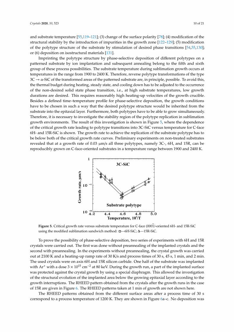
Imprinting the polytype structure by phase-selective deposition of different polytypes on apatterned substrate by ion implantation and subsequent annealing belong to the fifth and sixthgroup of these process possibilities. The substrate temperature during sublimation growth occurs attemperatures in the range from 1900 to 2400 K. Therefore, reverse polytype transformations of the type3C→ α-SiC of the transformed areas of the patterned substrate are, in principle, possible. To avoid this,the thermal budget during heating, steady state, and cooling down has to be adjusted to the occurrenceof the non-desired solid state phase transition, i.e., at high substrate temperatures, low growthdurations are desired. This requires reasonably high heating-up velocities of the growth crucible.Besides a defined time–temperature profile for phase-selective deposition, the growth conditionshave to be chosen in such a way that the desired polytype structure would be inherited from thesubstrate into the epitaxial layer. Furthermore, both polytypes have to be able to grow simultaneously.Therefore, it is necessary to investigate the stability region of the polytype replication in sublimationgrowth environments. The result of this investigation is shown in Figure 5, where the dependenceof the critical growth rate leading to polytype transitions into 3C-SiC versus temperature for C-face6H- and 15R-SiC is shown. The growth rate to achieve the replication of the substrate polytype has tobe below both of the critical growth rate curves. Preliminary experiments on non-treated substratesrevealed that at a growth rate of 0.03 µm/s all three polytypes, namely 3C-, 6H, and 15R, can bereproducibly grown on C-face-oriented substrates in a temperature range between 1900 and 2400 K.
Crystals 2020, 10, x FOR PEER REVIEW 10 of 21
avoid this, the thermal budget during heating, steady state, and cooling down has to be adjusted to the occurrence of the non-desired solid state phase transition, i.e., at high substrate temperatures, low growth durations are desired. This requires reasonably high heating-up velocities of the growth crucible. Besides a defined time–temperature profile for phase-selective deposition, the growth conditions have to be chosen in such a way that the desired polytype structure would be inherited from the substrate into the epitaxial layer. Furthermore, both polytypes have to be able to grow simultaneously. Therefore, it is necessary to investigate the stability region of the polytype replication in sublimation growth environments. The result of this investigation is shown in Figure 5, where the dependence of the critical growth rate leading to polytype transitions into 3C-SiC versus temperature for C-face 6H- and 15R-SiC is shown. The growth rate to achieve the replication of the substrate polytype has to be below both of the critical growth rate curves. Preliminary experiments on non-treated substrates revealed that at a growth rate of 0.03 µm/s all three polytypes, namely 3C-, 6H, and 15R, can be reproducibly grown on C-face-oriented substrates in a temperature range between 1900 and 2400 K.
Figure 5. Critical growth rate versus substrate temperature for C-face (0001)-oriented 6H- and 15R-SiC using the modified sublimation sandwich method: □ – 6H-SiC; Δ – 15R-SiC.
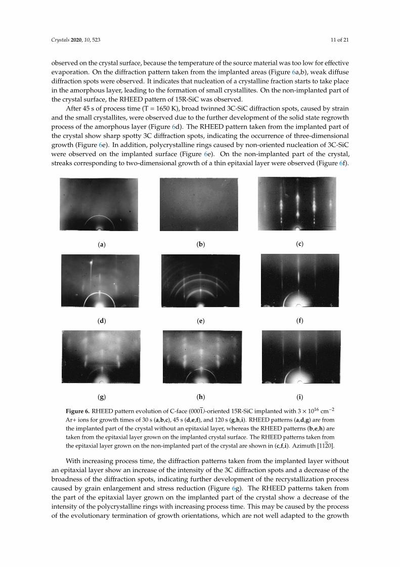
To prove the possibility of phase-selective deposition, two series of experiments with 6H and 15R crystals were carried out. The first was done without preannealing of the implanted crystals and the second with preannealing. In the experiments without preannealing, the crystal growth was carried out at 2100 K and a heating-up ramp rate of 30 K/s and process times of 30 s, 45 s, 1 min, and 2 min. The used crystals were on axis 6H and 15R silicon carbide. One half of the substrate was implanted with Ar+ with a dose 3 × 1015 cm−2 at 80 keV. During the growth run, a part of the implanted surface was protected against the crystal growth by using a special diaphragm. This allowed the investigation of the structural evolution of the implanted area below the growing epitaxial layer according to the growth interruptions. The RHEED pattern obtained from the crystals after the growth runs in the case of 15R are given in Figure 6. The RHEED patterns taken at 1 min of growth are not shown here.
The RHEED patterns obtained from the different surface areas after a process time of 30 s correspond to a process temperature of 1200 K. They are shown in Figure 6a–c. No deposition was observed on the crystal surface, because the temperature of the source material was too low for effective evaporation. On the diffraction pattern taken from the implanted areas (Figure 6a,b), weak diffuse diffraction spots were observed. It indicates that nucleation of a crystalline fraction starts to take place in the amorphous layer, leading to the formation of small crystallites. On the non-implanted part of the crystal surface, the RHEED pattern of 15R-SiC was observed.
3C-SiC
Substrate polytype
Figure 5. Critical growth rate versus substrate temperature for C-face (0001)-oriented 6H- and 15R-SiCusing the modified sublimation sandwich method: �—6H-SiC; ∆—15R-SiC.
To prove the possibility of phase-selective deposition, two series of experiments with 6H and 15Rcrystals were carried out. The first was done without preannealing of the implanted crystals and thesecond with preannealing. In the experiments without preannealing, the crystal growth was carriedout at 2100 K and a heating-up ramp rate of 30 K/s and process times of 30 s, 45 s, 1 min, and 2 min.The used crystals were on axis 6H and 15R silicon carbide. One half of the substrate was implantedwith Ar+ with a dose 3 × 1015 cm−2 at 80 keV. During the growth run, a part of the implanted surfacewas protected against the crystal growth by using a special diaphragm. This allowed the investigationof the structural evolution of the implanted area below the growing epitaxial layer according to thegrowth interruptions. The RHEED pattern obtained from the crystals after the growth runs in the caseof 15R are given in Figure 6. The RHEED patterns taken at 1 min of growth are not shown here.
The RHEED patterns obtained from the different surface areas after a process time of 30 scorrespond to a process temperature of 1200 K. They are shown in Figure 6a–c. No deposition was
Crystals 2020, 10, 523 11 of 21
observed on the crystal surface, because the temperature of the source material was too low for effectiveevaporation. On the diffraction pattern taken from the implanted areas (Figure 6a,b), weak diffusediffraction spots were observed. It indicates that nucleation of a crystalline fraction starts to take placein the amorphous layer, leading to the formation of small crystallites. On the non-implanted part ofthe crystal surface, the RHEED pattern of 15R-SiC was observed.
After 45 s of process time (T = 1650 K), broad twinned 3C-SiC diffraction spots, caused by strainand the small crystallites, were observed due to the further development of the solid state regrowthprocess of the amorphous layer (Figure 6d). The RHEED pattern taken from the implanted part ofthe crystal show sharp spotty 3C diffraction spots, indicating the occurrence of three-dimensionalgrowth (Figure 6e). In addition, polycrystalline rings caused by non-oriented nucleation of 3C-SiCwere observed on the implanted surface (Figure 6e). On the non-implanted part of the crystal,streaks corresponding to two-dimensional growth of a thin epitaxial layer were observed (Figure 6f).Crystals 2020, 10, x FOR PEER REVIEW 11 of 21
(a) (b) (c)
(d) (e) (f)
(g) (h) (i)
Figure 6. RHEED pattern evolution of C-face (0001)-oriented 15R-SiC implanted with 3 × 1016 cm−2 Ar+ ions for growth times of 30 s (a,b,c), 45 s (d,e,f), and 120 s (g,h,i). RHEED patterns (a,d,g) are from the implanted part of the crystal without an epitaxial layer, whereas the RHEED patterns (b,e,h) are taken from the epitaxial layer grown on the implanted crystal surface. The RHEED patterns taken from the epitaxial layer grown on the non-implanted part of the crystal are shown in (c,f,i). Azimuth [1120].
After 45 s of process time (T = 1650 K), broad twinned 3C-SiC diffraction spots, caused by strain and the small crystallites, were observed due to the further development of the solid state regrowth process of the amorphous layer (Figure 6d). The RHEED pattern taken from the implanted part of the crystal show sharp spotty 3C diffraction spots, indicating the occurrence of three-dimensional growth (Figure 6e). In addition, polycrystalline rings caused by non-oriented nucleation of 3C-SiC were observed on the implanted surface (Figure 6e). On the non-implanted part of the crystal, streaks corresponding to two-dimensional growth of a thin epitaxial layer were observed (Figure 6f).
With increasing process time, the diffraction patterns taken from the implanted layer without an epitaxial layer show an increase of the intensity of the 3C diffraction spots and a decrease of the broadness of the diffraction spots, indicating further development of the recrystallization process caused by grain enlargement and stress reduction (Figure 6g). The RHEED patterns taken from the part of the epitaxial layer grown on the implanted part of the crystal show a decrease of the intensity of the polycrystalline rings with increasing process time. This may be caused by the process of the evolutionary termination of growth orientations, which are not well adapted to the growth conditions [132] (Figure 6h). In the case of epitaxial growth on the non-implanted part of the crystal surface, 15R-SiC diffraction spots could be observed due to roughness development of the growing surface. This indicates that the polytype of the substrate was inherited to the epitaxial layer (Figure 6i). A similar behavior was found in the case of 6H-SiC.
In the case of epitaxial growth on crystals preannealed at temperatures leading to the formation of 3C-SiC in the implanted layer, the evolution of the RHEED pattern on the implanted and non-
Figure 6. RHEED pattern evolution of C-face (0001)-oriented 15R-SiC implanted with 3 × 1016 cm−2
Ar+ ions for growth times of 30 s (a,b,c), 45 s (d,e,f), and 120 s (g,h,i). RHEED patterns (a,d,g) are fromthe implanted part of the crystal without an epitaxial layer, whereas the RHEED patterns (b,e,h) aretaken from the epitaxial layer grown on the implanted crystal surface. The RHEED patterns taken fromthe epitaxial layer grown on the non-implanted part of the crystal are shown in (c,f,i). Azimuth [1120].
With increasing process time, the diffraction patterns taken from the implanted layer withoutan epitaxial layer show an increase of the intensity of the 3C diffraction spots and a decrease of thebroadness of the diffraction spots, indicating further development of the recrystallization processcaused by grain enlargement and stress reduction (Figure 6g). The RHEED patterns taken fromthe part of the epitaxial layer grown on the implanted part of the crystal show a decrease of theintensity of the polycrystalline rings with increasing process time. This may be caused by the processof the evolutionary termination of growth orientations, which are not well adapted to the growth
Crystals 2020, 10, 523 12 of 21
conditions [132] (Figure 6h). In the case of epitaxial growth on the non-implanted part of the crystalsurface, 15R-SiC diffraction spots could be observed due to roughness development of the growingsurface. This indicates that the polytype of the substrate was inherited to the epitaxial layer (Figure 6i).A similar behavior was found in the case of 6H-SiC.
In the case of epitaxial growth on crystals preannealed at temperatures leading to the formation of3C-SiC in the implanted layer, the evolution of the RHEED pattern on the implanted and non-implantedareas were comparable to the RHEED pattern’s development during the growth without preannealing.The only difference was the existence of 3C-SiC diffraction spots on the RHEED pattern receivedfrom the implanted areas at 45 s of process time. These patterns do not change in time in the case ofdiffraction from the area without epitaxial growth.
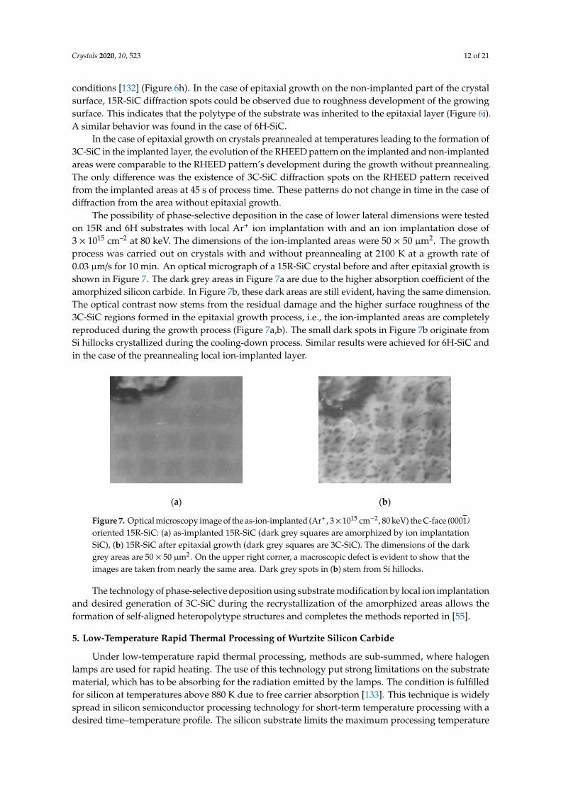
The possibility of phase-selective deposition in the case of lower lateral dimensions were testedon 15R and 6H substrates with local Ar+ ion implantation with and an ion implantation dose of3 × 1015 cm–2 at 80 keV. The dimensions of the ion-implanted areas were 50 × 50 µm2. The growthprocess was carried out on crystals with and without preannealing at 2100 K at a growth rate of0.03 µm/s for 10 min. An optical micrograph of a 15R-SiC crystal before and after epitaxial growth isshown in Figure 7. The dark grey areas in Figure 7a are due to the higher absorption coefficient of theamorphized silicon carbide. In Figure 7b, these dark areas are still evident, having the same dimension.The optical contrast now stems from the residual damage and the higher surface roughness of the3C-SiC regions formed in the epitaxial growth process, i.e., the ion-implanted areas are completelyreproduced during the growth process (Figure 7a,b). The small dark spots in Figure 7b originate fromSi hillocks crystallized during the cooling-down process. Similar results were achieved for 6H-SiC andin the case of the preannealing local ion-implanted layer.
Crystals 2020, 10, x FOR PEER REVIEW 12 of 21
implanted areas were comparable to the RHEED pattern’s development during the growth without preannealing. The only difference was the existence of 3C-SiC diffraction spots on the RHEED pattern received from the implanted areas at 45 s of process time. These patterns do not change in time in the case of diffraction from the area without epitaxial growth.
The possibility of phase-selective deposition in the case of lower lateral dimensions were tested on 15R and 6H substrates with local Ar+ ion implantation with and an ion implantation dose of 3 × 1015 cm-2 at 80 keV. The dimensions of the ion-implanted areas were 50 × 50 µm2. The growth process was carried out on crystals with and without preannealing at 2100 K at a growth rate of 0.03 µm/s for 10 min. An optical micrograph of a 15R-SiC crystal before and after epitaxial growth is shown in Figure 7. The dark grey areas in Figure 7a are due to the higher absorption coefficient of the amorphized silicon carbide. In Figure 7b, these dark areas are still evident, having the same dimension. The optical contrast now stems from the residual damage and the higher surface roughness of the 3C-SiC regions formed in the epitaxial growth process, i.e., the ion-implanted areas are completely reproduced during the growth process (Figure 7a,b). The small dark spots in Figure 7b originate from Si hillocks crystallized during the cooling-down process. Similar results were achieved for 6H-SiC and in the case of the preannealing local ion-implanted layer.
(a)
(b)
Figure 7. Optical microscopy image of the as-ion-implanted (Ar+, 3 × 1015 cm−2, 80 keV) the C-face (000 1 ) oriented 15R-SiC: (a) as-implanted 15R-SiC (dark grey squares are amorphized by ion implantation SiC), (b) 15R-SiC after epitaxial growth (dark grey squares are 3C-SiC). The dimensions of the dark grey areas are 50 × 50 µm2. On the upper right corner, a macroscopic defect is evident to show that the images are taken from nearly the same area. Dark grey spots in (b) stem from Si hillocks.
The technology of phase-selective deposition using substrate modification by local ion implantation and desired generation of 3C-SiC during the recrystallization of the amorphized areas allows the formation of self-aligned heteropolytype structures and completes the methods reported in [55].
5. Low-Temperature Rapid Thermal Processing of Wutzite Silicon Carbide
Under low-temperature rapid thermal processing, methods are sub-summed, where halogen lamps are used for rapid heating. The use of this technology put strong limitations on the substrate material, which has to be absorbing for the radiation emitted by the lamps. The condition is fulfilled for silicon at temperatures above 880 K due to free carrier absorption [133]. This technique is widely spread in silicon semiconductor processing technology for short-term temperature processing with a desired time–temperature profile. The silicon substrate limits the maximum processing temperature to 1720 K. 3C-SiC is typically formed if this technology or standard chemical vapor deposition for the growth of silicon carbide on silicon is used [19–22,134–140]. Far less publications can be found, which are devoted to the formation or growth of the hexagonal modifications of SiC on Si [32,141–146]. Therefore, there are a lack of methods to achieve the growth of hexagonal polytypes on silicon,
Figure 7. Optical microscopy image of the as-ion-implanted (Ar+, 3× 1015 cm−2, 80 keV) the C-face (0001)oriented 15R-SiC: (a) as-implanted 15R-SiC (dark grey squares are amorphized by ion implantationSiC), (b) 15R-SiC after epitaxial growth (dark grey squares are 3C-SiC). The dimensions of the darkgrey areas are 50 × 50 µm2. On the upper right corner, a macroscopic defect is evident to show that theimages are taken from nearly the same area. Dark grey spots in (b) stem from Si hillocks.
The technology of phase-selective deposition using substrate modification by local ion implantationand desired generation of 3C-SiC during the recrystallization of the amorphized areas allows theformation of self-aligned heteropolytype structures and completes the methods reported in [55].
5. Low-Temperature Rapid Thermal Processing of Wurtzite Silicon Carbide
Under low-temperature rapid thermal processing, methods are sub-summed, where halogenlamps are used for rapid heating. The use of this technology put strong limitations on the substratematerial, which has to be absorbing for the radiation emitted by the lamps. The condition is fulfilledfor silicon at temperatures above 880 K due to free carrier absorption [133]. This technique is widelyspread in silicon semiconductor processing technology for short-term temperature processing with adesired time–temperature profile. The silicon substrate limits the maximum processing temperature
Crystals 2020, 10, 523 13 of 21
to 1720 K. 3C-SiC is typically formed if this technology or standard chemical vapor deposition forthe growth of silicon carbide on silicon is used [19–22,134–140]. Far less publications can be found,which are devoted to the formation or growth of the hexagonal modifications of SiC on Si [32,141–146].Therefore, there are a lack of methods to achieve the growth of hexagonal polytypes on silicon,especially the rare polytype 2H. This possibility is a precondition to realize phase-selective epitaxy ofSiC on Si. The challenge can be addressed using different approaches: (1) The growth of 2H-SiC undernon-equilibrium conditions [32,121,141,145,147]; (2) the growth of 2H-SiC under specific nucleationand growth conditions [122,126,148–152]; and (3) growth of 2H-SiC on isostructural non-silicon carbidematerials [131].
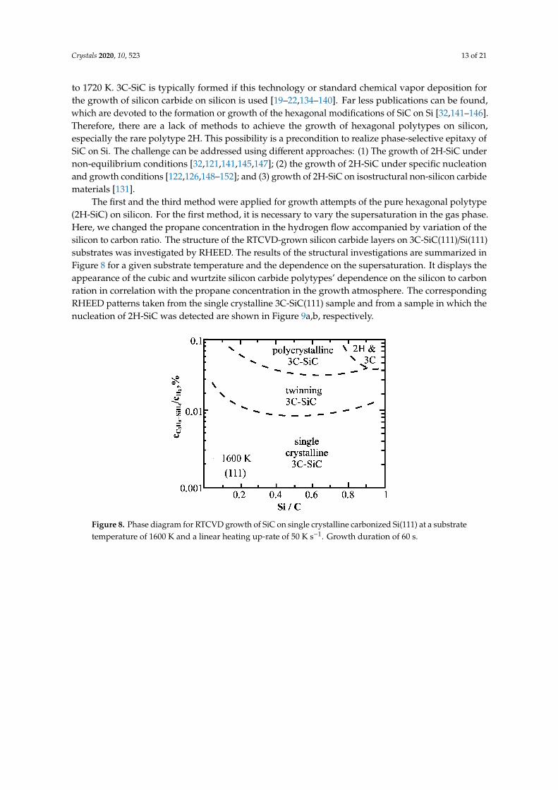
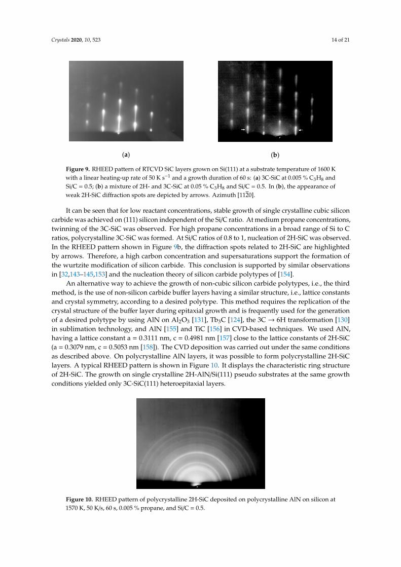
The first and the third method were applied for growth attempts of the pure hexagonal polytype(2H-SiC) on silicon. For the first method, it is necessary to vary the supersaturation in the gas phase.Here, we changed the propane concentration in the hydrogen flow accompanied by variation of thesilicon to carbon ratio. The structure of the RTCVD-grown silicon carbide layers on 3C-SiC(111)/Si(111)substrates was investigated by RHEED. The results of the structural investigations are summarized inFigure 8 for a given substrate temperature and the dependence on the supersaturation. It displays theappearance of the cubic and wurtzite silicon carbide polytypes’ dependence on the silicon to carbonration in correlation with the propane concentration in the growth atmosphere. The correspondingRHEED patterns taken from the single crystalline 3C-SiC(111) sample and from a sample in which thenucleation of 2H-SiC was detected are shown in Figure 9a,b, respectively.
Figure 8. Phase diagram for RTCVD growth of SiC on single crystalline carbonized Si(111) at a substratetemperature of 1600 K and a linear heating up-rate of 50 K s−1. Growth duration of 60 s.
Crystals 2020, 10, 523 14 of 21
Crystals 2020, 10, x FOR PEER REVIEW 13 of 21
especially the rare polytype 2H. This possibility is a precondition to realize phase-selective epitaxy of SiC on Si. The challenge can be addressed using different approaches: (1) The growth of 2H-SiC under non-equilibrium conditions [32,121,141,145,147]; (2) the growth of 2H-SiC under specific nucleation and growth conditions [122,126,148–152]; and (3) growth of 2H-SiC on isostructural non-silicon carbide materials [131].
The first and the third method were applied for growth attempts of the pure hexagonal polytype (2H-SiC) on silicon. For the first method, it is necessary to vary the supersaturation in the gas phase. Here, we changed the propane concentration in the hydrogen flow accompanied by variation of the silicon to carbon ratio. The structure of the RTCVD-grown silicon carbide layers on 3C-SiC(111)/Si(111) substrates was investigated by RHEED. The results of the structural investigations are summarized in Figure 8 for a given substrate temperature and the dependence on the supersaturation. It displays the appearance of the cubic and wurtzite silicon carbide polytypes’ dependence on the silicon to carbon ration in correlation with the propane concentration in the growth atmosphere. The corresponding RHEED patterns taken from the single crystalline 3C-SiC(111) sample and from a sample in which the nucleation of 2H-SiC was detected are shown in Figure 9a,b, respectively.
Figure 8. Phase diagram for RTCVD growth of SiC on single crystalline carbonized Si(111) at a substrate temperature of 1600 K and a linear heating up-rate of 50 K s-1. Growth duration of 60 s.
(a)
(b)
Figure 9. RHEED pattern of RTCVD SiC layers grown on Si(111) at a substrate temperature of 1600 K with a linear heating-up rate of 50 K s−1 and a growth duration of 60 s: (a) 3C-SiC at 0.005 % C3H8 and Si/C = 0.5; (b) a mixture of 2H- and 3C-SiC at 0.05 % C3H8 and Si/C = 0.5. In (b), the appearance of weak 2H-SiC diffraction spots are depicted by arrows. Azimuth [1120].
1600 K
Figure 9. RHEED pattern of RTCVD SiC layers grown on Si(111) at a substrate temperature of 1600 Kwith a linear heating-up rate of 50 K s−1 and a growth duration of 60 s: (a) 3C-SiC at 0.005 % C3H8 andSi/C = 0.5; (b) a mixture of 2H- and 3C-SiC at 0.05 % C3H8 and Si/C = 0.5. In (b), the appearance ofweak 2H-SiC diffraction spots are depicted by arrows. Azimuth [1120].
It can be seen that for low reactant concentrations, stable growth of single crystalline cubic siliconcarbide was achieved on (111) silicon independent of the Si/C ratio. At medium propane concentrations,twinning of the 3C-SiC was observed. For high propane concentrations in a broad range of Si to Cratios, polycrystalline 3C-SiC was formed. At Si/C ratios of 0.8 to 1, nucleation of 2H-SiC was observed.In the RHEED pattern shown in Figure 9b, the diffraction spots related to 2H-SiC are highlightedby arrows. Therefore, a high carbon concentration and supersaturations support the formation ofthe wurtzite modification of silicon carbide. This conclusion is supported by similar observationsin [32,143–145,153] and the nucleation theory of silicon carbide polytypes of [154].
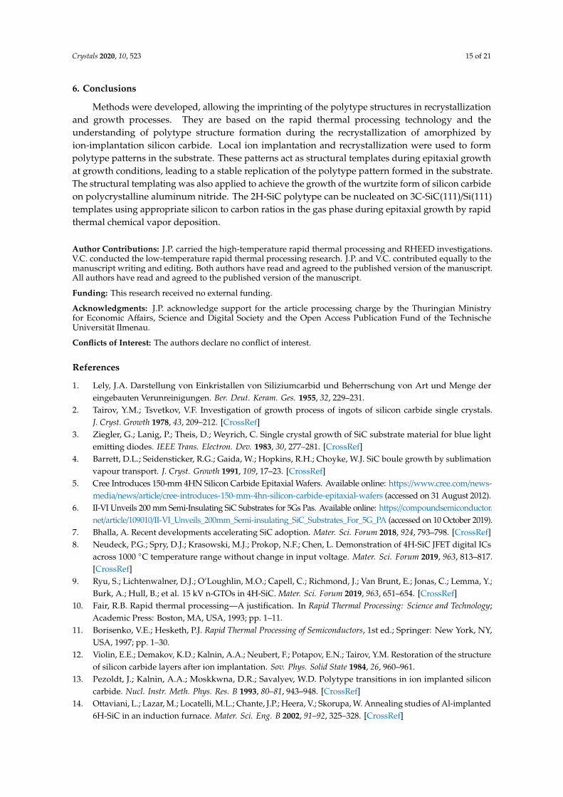
An alternative way to achieve the growth of non-cubic silicon carbide polytypes, i.e., the thirdmethod, is the use of non-silicon carbide buffer layers having a similar structure, i.e., lattice constantsand crystal symmetry, according to a desired polytype. This method requires the replication of thecrystal structure of the buffer layer during epitaxial growth and is frequently used for the generationof a desired polytype by using AlN on Al2O3 [131], Tb3C [124], the 3C→ 6H transformation [130]in sublimation technology, and AlN [155] and TiC [156] in CVD-based techniques. We used AlN,having a lattice constant a = 0.3111 nm, c = 0.4981 nm [157] close to the lattice constants of 2H-SiC(a = 0.3079 nm, c = 0.5053 nm [158]). The CVD deposition was carried out under the same conditionsas described above. On polycrystalline AlN layers, it was possible to form polycrystalline 2H-SiClayers. A typical RHEED pattern is shown in Figure 10. It displays the characteristic ring structureof 2H-SiC. The growth on single crystalline 2H-AlN/Si(111) pseudo substrates at the same growthconditions yielded only 3C-SiC(111) heteroepitaxial layers.
Crystals 2020, 10, x FOR PEER REVIEW 14 of 21
It can be seen that for low reactant concentrations, stable growth of single crystalline cubic silicon carbide was achieved on (111) silicon independent of the Si/C ratio. At medium propane concentrations, twinning of the 3C-SiC was observed. For high propane concentrations in a broad range of Si to C ratios, polycrystalline 3C-SiC was formed. At Si/C ratios of 0.8 to 1, nucleation of 2H-SiC was observed. In the RHEED pattern shown in Figure 9b, the diffraction spots related to 2H-SiC are highlighted by arrows. Therefore, a high carbon concentration and supersaturations support the formation of the wurtzite modification of silicon carbide. This conclusion is supported by similar observations in [32,143–145,153] and the nucleation theory of silicon carbide polytypes of [154].
An alternative way to achieve the growth of non-cubic silicon carbide polytypes, i.e., the third method, is the use of non-silicon carbide buffer layers having a similar structure, i.e., lattice constants and crystal symmetry, according to a desired polytype. This method requires the replication of the crystal structure of the buffer layer during epitaxial growth and is frequently used for the generation of a desired polytype by using AlN on Al2O3 [131], Tb3C [124], the 3C → 6H transformation [130] in sublimation technology, and AlN [155] and TiC [156] in CVD-based techniques. We used AlN, having a lattice constant a = 0.3111 nm, c = 0.4981 nm [157] close to the lattice constants of 2H-SiC (a = 0.3079 nm, c = 0.5053 nm [158]). The CVD deposition was carried out under the same conditions as described above. On polycrystalline AlN layers, it was possible to form polycrystalline 2H-SiC layers. A typical RHEED pattern is shown in Figure 10. It displays the characteristic ring structure of 2H-SiC. The growth on single crystalline 2H-AlN/Si(111) pseudo substrates at the same growth conditions yielded only 3C-SiC(111) heteroepitaxial layers.
Figure 10. RHEED pattern of polycrystalline 2H-SiC deposited on polycrystalline AlN on silicon at 1570 K, 50 K/s, 60 s, 0,005 % propane, and Si/C = 0,5.
6. Conclusions
Methods were developed, allowing the imprinting of the polytype structures in recrystallization and growth processes. They are based on the rapid thermal processing technology and the understanding of polytype structure formation during the recrystallization of amorphized by ion-implantation silicon carbide. Local ion implantation and recrystallization were used to form polytype patterns in the substrate. These patterns act as structural templates during epitaxial growth at growth conditions, leading to a stable replication of the polytype pattern formed in the substrate. The structural templating was also applied to achieve the growth of the wurtzite form of silicon carbide on polycrystalline aluminum nitride. The 2H-SiC polytype can be nucleated on 3C-SiC(111)/Si(111) templates using appropriate silicon to carbon ratios in the gas phase during epitaxial growth by rapid thermal chemical vapor deposition.
Author Contributions: J.P. carried the high-temperature rapid thermal processing and RHEED investigations. V.C. conducted the low-temperature rapid thermal processing research. J.P. and V.C. contributed equally to the manuscript writing and editing. Both authors have read and agreed to the published version of the manuscript.
Funding: This research received no external funding.
Figure 10. RHEED pattern of polycrystalline 2H-SiC deposited on polycrystalline AlN on silicon at1570 K, 50 K/s, 60 s, 0.005 % propane, and Si/C = 0.5.
Crystals 2020, 10, 523 15 of 21
6. Conclusions
Methods were developed, allowing the imprinting of the polytype structures in recrystallizationand growth processes. They are based on the rapid thermal processing technology and theunderstanding of polytype structure formation during the recrystallization of amorphized byion-implantation silicon carbide. Local ion implantation and recrystallization were used to formpolytype patterns in the substrate. These patterns act as structural templates during epitaxial growthat growth conditions, leading to a stable replication of the polytype pattern formed in the substrate.The structural templating was also applied to achieve the growth of the wurtzite form of silicon carbideon polycrystalline aluminum nitride. The 2H-SiC polytype can be nucleated on 3C-SiC(111)/Si(111)templates using appropriate silicon to carbon ratios in the gas phase during epitaxial growth by rapidthermal chemical vapor deposition.
Author Contributions: J.P. carried the high-temperature rapid thermal processing and RHEED investigations.V.C. conducted the low-temperature rapid thermal processing research. J.P. and V.C. contributed equally to themanuscript writing and editing. Both authors have read and agreed to the published version of the manuscript.All authors have read and agreed to the published version of the manuscript.
Funding: This research received no external funding.
Acknowledgments: J.P. acknowledge support for the article processing charge by the Thuringian Ministryfor Economic Affairs, Science and Digital Society and the Open Access Publication Fund of the TechnischeUniversität Ilmenau.
Conflicts of Interest: The authors declare no conflict of interest.
References
1. Lely, J.A. Darstellung von Einkristallen von Siliziumcarbid und Beherrschung von Art und Menge dereingebauten Verunreinigungen. Ber. Deut. Keram. Ges. 1955, 32, 229–231.
2. Tairov, Y.M.; Tsvetkov, V.F. Investigation of growth process of ingots of silicon carbide single crystals.J. Cryst. Growth 1978, 43, 209–212. [CrossRef]
3. Ziegler, G.; Lanig, P.; Theis, D.; Weyrich, C. Single crystal growth of SiC substrate material for blue lightemitting diodes. IEEE Trans. Electron. Dev. 1983, 30, 277–281. [CrossRef]
4. Barrett, D.L.; Seidensticker, R.G.; Gaida, W.; Hopkins, R.H.; Choyke, W.J. SiC boule growth by sublimationvapour transport. J. Cryst. Growth 1991, 109, 17–23. [CrossRef]
5. Cree Introduces 150-mm 4HN Silicon Carbide Epitaxial Wafers. Available online: https://www.cree.com/news-media/news/article/cree-introduces-150-mm-4hn-silicon-carbide-epitaxial-wafers (accessed on 31 August 2012).
6. II-VI Unveils 200 mm Semi-Insulating SiC Substrates for 5Gs Pas. Available online: https://compoundsemiconductor.net/article/109010/II-VI_Unveils_200mm_Semi-insulating_SiC_Substrates_For_5G_PA (accessed on 10 October 2019).
7. Bhalla, A. Recent developments accelerating SiC adoption. Mater. Sci. Forum 2018, 924, 793–798. [CrossRef]8. Neudeck, P.G.; Spry, D.J.; Krasowski, M.J.; Prokop, N.F.; Chen, L. Demonstration of 4H-SiC JFET digital ICs
across 1000 ◦C temperature range without change in input voltage. Mater. Sci. Forum 2019, 963, 813–817.[CrossRef]
9. Ryu, S.; Lichtenwalner, D.J.; O’Loughlin, M.O.; Capell, C.; Richmond, J.; Van Brunt, E.; Jonas, C.; Lemma, Y.;Burk, A.; Hull, B.; et al. 15 kV n-GTOs in 4H-SiC. Mater. Sci. Forum 2019, 963, 651–654. [CrossRef]
10. Fair, R.B. Rapid thermal processing—A justification. In Rapid Thermal Processing: Science and Technology;Academic Press: Boston, MA, USA, 1993; pp. 1–11.
11. Borisenko, V.E.; Hesketh, P.J. Rapid Thermal Processing of Semiconductors, 1st ed.; Springer: New York, NY,USA, 1997; pp. 1–30.
12. Violin, E.E.; Demakov, K.D.; Kalnin, A.A.; Neubert, F.; Potapov, E.N.; Tairov, Y.M. Restoration of the structureof silicon carbide layers after ion implantation. Sov. Phys. Solid State 1984, 26, 960–961.
13. Pezoldt, J.; Kalnin, A.A.; Moskkwna, D.R.; Savalyev, W.D. Polytype transitions in ion implanted siliconcarbide. Nucl. Instr. Meth. Phys. Res. B 1993, 80–81, 943–948. [CrossRef]
14. Ottaviani, L.; Lazar, M.; Locatelli, M.L.; Chante, J.P.; Heera, V.; Skorupa, W. Annealing studies of Al-implanted6H-SiC in an induction furnace. Mater. Sci. Eng. B 2002, 91–92, 325–328. [CrossRef]
Crystals 2020, 10, 523 16 of 21
15. Wang, Z.; Liu, W.; Wang, C. Recent progress in ohmic contacts to silicon carbide for high-temperatureapplications. J. Electron. Mater. 2016, 45, 267–284. [CrossRef]
16. Porter, L.M.; Davis, R.F. A critical review of ohmic and rectifying contacts for silicon carbide. Mater. Sci.Eng. B 1995, 34, 83–105. [CrossRef]
17. Vasilevskiy, K.; Zekentes, K.; Wright, N. Processing and characterization of ohmic contacts to silicon carbide.Adv. Res. Found. 2018, 37, 27–126.
18. Roccaforte, F.; Brezeanu, G.; Ganmon, P.M.; Giannazzo, F.; Rascuna, S.; Saggio, M. Schottky contacts to siliconcarbide: Physics, technology and applications. Adv. Res. Found. 2018, 37, 127–190.
19. Steckl, A.J.; Li, J.P. Rapid thermal chemical vapour deposition growth of nanometer-thin SiC on silicon.Thin Solid Films 1992, 216, 149–154. [CrossRef]
20. Cimalla, V.; Karagodina, K.V.; Pezoldt, J.; Eichhorn, G. Growth of thin ß-SiC layers by carbonization of Sisurfaces by rapid thermal processing. Mater. Sci. Eng. B 1995, 29, 170–175. [CrossRef]
21. Steckl, A.J.; Li, J.P. Epitaxial growth of beta-SiC on Si by RTCVD with C3H8 and SiH4. IEEE Trans. Electron Dev.1992, 39, 64–74. [CrossRef]
22. Cimalla, V.; Pezoldt, J.; Ecke, G.; Eichhorn, G. The buffer layer in RTCVD of SiC. Inst. Phys. Conf. Ser.1996, 142, 153–156.
23. Skorupa, W.; Panknin, D.; Anwand, W.; Voelskow, M.; Ferro, G.; Monteil, Y.; Leycuras, A.; Pezoldt, J.;McMahon, R.; Smith, M.; et al. Flash lamp supported deposition of 3C-SiC (FLASiC)—A promising techniqueto produce high quality cubic SiC layers. Mater. Sci. Forum 2004, 457–460, 175–180. [CrossRef]
24. Pezoldt, J.; Morales, F.M.; Stauden, T.; Förster, C.; Polychroniadis, E.; Stoemenos, J.; Panknin, D.; Skorupa, W.Growth acceleration in FLASiC assisted short time liquid phase epitaxy by melt modification. Mater. Sci. Forum2006, 527–529, 295–298. [CrossRef]
25. Pezoldt, J.; Kups, T.; Stauden, T.; Schröter, B. Polarity determination and control of SiC grown on Si. Mater.Sci. Eng. B 2009, 165, 28–33. [CrossRef]
26. As, D.J.; Frey, T.; Schikora, D.; Lischka, K.; Cimalla, V.; Pezoldt, J.; Goldhahn, R.; Kaiser, S.; Gebhardt, W.Cubic GaN epilayers grown by molecular beam epitaxy on thin ß-SiC/Si(001) substrates. Appl. Phys. Lett.2000, 76, 1686–1688. [CrossRef]
27. Lorenz, M.; Hochmuth, H.; Jammoul, A.; Ferro, G.; Förster, C.; Pezoldt, J.; Perez, J.Z.; Benndorf, G.; Lenzner, J.;Schmidt-Grund, R.; et al. Luminescence of ZnO thin films grown on pulsed laser deposition on 3C-SiCbufferred Si. Wiss. Techn. Ber. FZR 2005, 433, 74–82.
28. Chiew, S.P.; McBride, G.; Amstrong, B.M.; Grimshaw, J.; Gamble, H.S.; Trocha-Grimshaw, J. Growth ofbeta-SiC layers by rapid thermal chemical vapour deposition. Microelectron. Eng. 1994, 25, 177–182.[CrossRef]
29. Yih, P.H.; Li, J.P.; Steckl, A.J. SiC/Si heterojunction diodes fabricated by self-selective and by blanket rapidthermal chemical vapour deposition. IEEE Trans. Electron. Dev. 1994, 41, 281–287. [CrossRef]
30. Verma, A.R.; Krishna, P. Polymorphism and Polytypism in Crystals; John Wiley & Sons: New York, NY, USA,1966; pp. 8–91.
31. Von Münch, W.; Pfaffeneder, I. Epitaxial deposition of silicon carbide from silicon tetrachloride and hexane.Thin Solid Films 1976, 31, 39–51. [CrossRef]
32. Shinozaki, S.S.; Sato, H. Microstructure of SiC prepared by chemical vapour deposition. J. Am. Ceram. Soc.1978, 61, 425–429. [CrossRef]
33. Kalnin, A.A.; Luchinin, V.V.; Neubert, F.; Tairov, Y.M. Crystal structure formation during synthesis ofsubstances with multiple structurally stable states. Sov. Phys. Tech. Phys. 1984, 29, 807–809.
34. Fisher, G.R.; Barnes, P. Towards a unified view of polytypism in silicon carbide. Philos. Mag. B 1990, 61, 217–236.[CrossRef]
35. Agrosi, G.; Tempesta, G.; Capitani, G.C.; Scandale, E.; Siche, D. Multi-analytical study of syntactic coalescenceof polytypes in a 6H-SiC sample. J. Cryst. Growth 2009, 311, 4784–4790. [CrossRef]
36. Avrov, D.D.; Lebedev, A.O.; Tairov, Y.M. Polytype inclusions and polytype stability in silicon-carbide crystals.Semiconductors 2016, 50, 494–501. [CrossRef]
37. Lebedev, A.A. Heterojunctions and superlattices based on silicon carbide. Semicond. Sci. Technol.2006, 21, R17–R34. [CrossRef]
38. Pezoldt, J. Are polytype transitions possible during boron diffusion? Mater. Sci. Eng. B 1995, 29, 99–104.[CrossRef]
Crystals 2020, 10, 523 17 of 21
39. Pezoldt, J.; Stottko, B.; Kupris, G.; Ecke, G. Sputtering effects in hexagonal silicon carbide. Mater. Sci. Eng.1995, 29, 94–98. [CrossRef]
40. Camara, N.; Thuaire, A.; Bano, E.; Zekentes, K. Forward-bias degradation in 4H-SiC p+nn+ diodes: Influenceof mesa etching. Phys. Status Solidi A 2005, 202, 660–664. [CrossRef]
41. Moskvina, D.R.; Pezoldt, J.; Potapov, E.N.; Tairov, Y.M. Polytypic phase transitions induced by ionimplantation. Sov. Phys. Semicond. 1989, 23, 1388–1389.
42. Pezoldt, J.; Moskvina, D.R. Nonequilibrium phase transition in silicon carbide crystals. Sov. Tech. Phys. Lett.1992, 18, 432–433.
43. Ohno, T.; Koboyashi, N. Difference of secondary defect formation by high energy B+ and Al+ implantationinto 4H-SiC. J. Appl. Phys. 2002, 91, 4136–4142. [CrossRef]
44. Okojie, R.S.; Zhang, M.; Pirouz, P.; Tumakha, S.; Jessen, G.; Brillson, L.J. Observation of 4H-SiC to 3C-SiCpolytypic transformation during oxidation. Appl. Phys. Lett. 2001, 79, 3056–3058. [CrossRef]
45. Tumakha, S.; Brillson, L.J.; Jessen, G.H.; Okojie, R.S.; Lukco, D.; Zhang, M.; Pirouz, P. Chemically dependenttraps and polytypes at Pt/Ti contacts to 4H and 6H–SiC and metallization. J. Vac. Sci. Technol. B2002, 20, 554–560. [CrossRef]
46. Tumakha, S.; Goss, S.H.; Brillson, L.J.; Okojie, R.S. Electronic states at annealed metal/4H-SiC interfaces.J. Vac. Sci. Technol. 2005, 23, 594–598. [CrossRef]
47. Brigden, C.T.; Farnan, I.; Hania, P.R. Multi-nuclear NMR study of polytype and defect distribution in neutronirradiated silicon carbide. J. Nucl. Mater. 2014, 444, 92–100. [CrossRef]
48. Brigden, C.T.; Farnan, I.; Hania, P.R. Corrigendum to “Multi-nuclear NMR study of polytype and defectdistribution in neutron irradiated silicon carbide” [J. Nucl. Mater. 444 (2014) 92–100]. J. Nucl. Mater.2014, 446, 257. [CrossRef]
49. Ziegler, G.; Theis, D. A new degradation phenomena in blue light emitting silicon carbide diodes. IEEE Trans.Electron. Dev. 1981, 28, 425–427. [CrossRef]
50. Skowronski, M.; Ha, S. Degradation of hexagonal silicon-carbide-based bipolar devices. J. Appl. Phys.2006, 99, 011101. [CrossRef]
51. Konishi, K.; Fujita, R.; Mori, Y.; Shima, A. Inducing defects in 3.3 kV SiC MOSFETs by annealing after ionimplantation and evaluating their effect on bipolar degradation of the MOSFETs. Semicond. Sci. Technol.2018, 33, 125014. [CrossRef]
52. Dubrovskii, G.B. Superstructure, energy spectrum, and polytypism of silicon carbide crystals. Sov. Phys.Solid State 1972, 13, 2107.
53. Powell, J.A.; Petit, J.B.; Edgar, J.H.; Jenkins, I.G.; Matus, L.G.; Yang, J.W.; Pirouz, P.; Choyke, W.J.; Clemen, L.;Yoganathan, M. Controlled growth of 3C-SiC and 6H-SiC films on low-tilt-angle vicinal (0001). Appl. Phys.Lett. 1991, 59, 333–335. [CrossRef]
54. Pezoldt, J.; Kalnin, A.A.; Savelyev, W.D. Application of nonequilibrium phase transition to heteropolytypestructure creation. Nucl. Instr. Meth. Phys. Res. B 1992, 65, 361–365. [CrossRef]
55. Kalnin, A.A.; Neubert, F.; Pezoldt, J. Polytype patterning in epitaxial layers on the basis of non-equilibriumphase transitions. Diam. Relat. Mater. 1994, 3, 346–352. [CrossRef]
56. Pezoldt, J.; Kalnin, A.A.; Savelyev, W.D. Desired β-SiC inclusions in α-SiC epitaxial layers by ion implantationassisted information centre creation. Z. Kristallogr. 1994, 8, 550.
57. Fissel, A. Artificially layered heteropolytype structure based on SiC polytypes: Molecular beam epitaxy,characterization and properties. Phys. Rep. 2003, 379, 149–255. [CrossRef]
58. Pezoldt, J.; Morales, F.M.; Kalnin, A.A. Local control of SiC polytypes. Phys. Status Solidi A 2007, 204, 1056–1062.[CrossRef]
59. Chandrashekhar, M.V.; Thomas, C.I.; Lu, J.; Spencer, M.G. Observation of a two dimensional electron gasformed in a polarization doped C-face 3C/4H SiC heteropolytypic junction. Appl. Phys. Lett. 2007, 91, 033503.[CrossRef]
60. Lu, J.; Thomas, C.I.; Chandrashekhar, V.S.; Spencer, M.G. Measurement of spontaneous polarization inC-face 3C-SiC/6H-SiC heterostructures with two-dimensional electron gas by capacitance-voltage method.J. Appl. Phys. 2009, 105, 106108. [CrossRef]
61. Polyakov, V.M.; Schwierz, F. Formation of two-dimensional electron gases in polytypic heterostructures.J. Appl. Phys. 2005, 98, 023709. [CrossRef]
Crystals 2020, 10, 523 18 of 21
62. Matsushita, Y.-I.; Oshiyama, A. Interstitial channels that control band gaps and effective masses in tetrahedrallybonded semiconductors. Phys. Rev. Lett. 2014, 112, 136403. [CrossRef]
63. Gao, G.-B.; Morkoc, H. Material-based comparison for power heterojunction bipolar transistors. IEEE Trans.Electron. Dev. 1991, 38, 2410–2416. [CrossRef]
64. Gao, G.-B.; Morkoc, H. High frequency performance of SiC heterojunction bipolar transistors. IEEE Trans.Electron. Dev. 1994, 41, 1092–1097.
65. Iwata, H.; Lindefelt, U.; Öberg, S.; Briddon, P.R. A new type of quantum wells: Stacking faults in siliconcarbide. Microelectr. J. 2003, 34, 371–374. [CrossRef]
66. Davydov, S.Y.; Lebedev, A.A.; Posrednik, O.V. Estimation of the exciton transition energy in NH/3C/NH(N = 2, 4, 6, 8) heterostructures based on silicon carbide polytypes. Semiconductors 2006, 40, 549–553.[CrossRef]
67. Davydov, S.Y.; Posrednik, O.V. The energy levels in quantum wells formed at the contacts between cubic andhexagonal polytypes of silicon carbide. Tech. Phys. Lett. 2005, 31, 746–748. [CrossRef]
68. Bechstedt, F.; Käckell, P. Heterocrystalline structures: New types of superlattices? Phys. Rev. Lett.1995, 75, 2180–2183. [CrossRef] [PubMed]
69. Miao, M.S.; Lambrecht, W.R.L. Electronic structure of thin heterocrystalline superlattices in SiC and AlN.Phys. Rev. B 2003, 68, 155320. [CrossRef]
70. Deak, P.; Buruzs, A.; Gali, A.; Frauenheim, T.; Choyke, W.J. Silicon carbide: A playground for 1D-modulationelectronics. Mater. Sci. Forum 2006, 527–529, 355–358. [CrossRef]
71. Matsushita, Y.-I.; Furuya, S.; Oshiyama, A. Electron confinement due to stacking control of atomic layersin SiC polytypes: Role of floating states and spontaneous polarization. J. Phys. Soc. Jpn. 2014, 83, 094713.[CrossRef]
72. Sugihara, Y.; Ichida, K.; Oshiyama, A. Electron and hole confinement in hetero-crystalline SiC superlattice.J. Phys. Soc. Jpn. 2015, 84, 084709. [CrossRef]
73. Pezoldt, J. Heteropolytypic superlattices. Mater. Sci. Forum 2016, 858, 278–282. [CrossRef]74. Lebedev, A.A.; Zamorianskaya, M.V.; Davydov, S.Y.; Kirilenko, D.A.; Lebedev, S.P.; Sorokin, L.M.;
Shustov, D.B.; Scheglov, M.P. Investigation of the transition layer in 3C-SiC/6H-SiC heterostructures.Semiconductors 2013, 47, 1539–1543. [CrossRef]
75. Davydov, S.Y.; Lebedev, A.A.; Usikov, A.S. On specific features of silicon carbide heteropolytype epitaxy.Sci. Tech. J. Inf. Technol. Mech. Opt. 2015, 15, 632–639. [CrossRef]
76. Carlsson, J.O. Selective vapour phase deposition on patterned substrates. Crit. Rev. Solid State1990, 16, 217–236. [CrossRef]
77. Janusonis, S.; Janusoniene, V. Self—Formation of the artificial planar systems: Theory and applications.Solid State Phenom. 2004, 97–98, 259–491. [CrossRef]
78. Stein, R.A.; Lanig, P.; Leibenzeder, S. Influence of surface energy on the growth of 6H- and 4H-SiC polytypesby sublimation. Mater. Sci. Eng. B 1992, 11, 69–71. [CrossRef]
79. Arbel, A.; Natan, M. Effective diffusion time during rapid thermal processing. J. Appl. Phys. 1987, 61, 1209–1210.[CrossRef]
80. Leitz, G.; Pezoldt, J.; Patzschke, I.; Zöllner, J.-P.; Eichhorn, G. Investigation of dynamical temperaturebehaviour in RTP. Mater. Res. Symp. Proc. 1992, 303, 171–178. [CrossRef]
81. Cimalla, V.; Stauden, T.; Eichhorn, G.; Pezoldt, J. Influence of the heating ramp on the heteroepitaxial growthof SiC on Si. Mater. Sci. Eng. B 1999, 61–62, 553–558. [CrossRef]
82. Michel, P.; Gauthier, J.P. Etude du polytypisme des cristaux de carbure de silicium par diffraction electroniquepar reflexion. J. Appl. Cryst. 1976, 9, 318–324. [CrossRef]
83. Gauthier, J.P.; Duc, B.M.; Michel, P. Polytypisme du carbure de silicium: Diffraction electronique et simulationoptique. J. Appl. Cryst. 1977, 10, 111–117. [CrossRef]
84. Neubert, F.; Pezoldt, J. Investigation of the surface of silicon carbide with electron diffraction. Isv. LETI1983, 322, 58–64. (In Russian)
85. Scharmann, F.; Pezoldt, J. RHEED: A Tool for Structural Investigations of thin polytypic SiC layers. Mater.Sci. Forum 2002, 389–393, 463–466. [CrossRef]
86. Shinozaki, S.; Sato, H. One-dimensional disordered structure and polytypism in SiC. Mater. Res. Bull.1975, 10, 257–260.
Crystals 2020, 10, 523 19 of 21
87. Shinozaki, S.; Kinsman, K.R. Aspects of “one dimensional disorder” in silicon carbide. Acta Metall.1978, 26, 769–776. [CrossRef]
88. Sakata, T.; Mori, H.; Yasuda, H.; Fujita, H. Crystallization of platinum implanted amorphous SiC. J. Electron.Microsc. 1992, 41, 185–189.
89. Mori, H.; Sakata, T. High-resolution electron microscopy study on crystallization of gold implantedamorphous SiC. Nucl. Instr. Meth. Phys. Res. B 1994, 94, 73–80. [CrossRef]
90. Dubey, M.; Singh, G. Recrystallization of SiC thin films. J. Phys. D Appl. Phys. 1974, 7, 1482–1484. [CrossRef]91. Bentley, J.; Romana, L.J.; Horton, L.L.; McHargue, C.J. Distribution and characterization of iron in implanted
silicon carbide. Mater. Res. Soc. Symp. Proc. 1992, 235, 363–368. [CrossRef]92. Heera, V.; Kögler, R.; Skorupa, W.; Stoemenos, J. Complete recrystallization of amorphous silicon carbide
layers by ion radiation. Appl. Phys. Lett. 1995, 67, 1999–2001. [CrossRef]93. Bohn, H.G.; Williams, J.M.; McHargue, C.J.; Begun, G.M. Recrystallization of ion-implanted α-SiC. J. Mater.
Res. 1987, 2, 107–116. [CrossRef]94. Heindl, J.; Strunk, H.P.; Heft, A.; Bachmann, T.; Glaser, E.; Wendler, E.; Wesch, W. Ion-implantation and
annealing of 6H-SiC. Inst. Phys. Conf. Ser. 1995, 146, 435–438.95. Pacaud, Y.; Skorupa, W.; Stoemenos, J. Microstructural characterization of amorphized and recrystallized
6H-SiC. Nucl. Instr. Meth. Phys. Res. B 1996, 120, 181–185. [CrossRef]96. Bae, I.-T.; Ishimaru, M.; Hirotsu, Y.; Sickafus, K.E. Solid phase epitaxy of amorphous silicon carbide:
Ion fluence dependence. J. Appl. Phys. 2004, 96, 1451–1457. [CrossRef]97. Eryu, O.; Abe, K.; Nakashima, K.; Harima, H. Kinetics of sold phase regrowth of self-ion-implanted
amorphous SiC during low temperature furnace annealing. Nucl. Instr. Meth. Phys. Res. B 2003, 206, 969–973.[CrossRef]
98. Williams, J.S. Solid phase epitaxial regrowth phenomena in silicon. Nucl. Instr. Meth. Res. 1983, 209–210,219–228. [CrossRef]
99. Savaraliev, G.K.; Tairov, Y.M.; Tsvetkov, V.F.; Chernov, M.A. On the transfer of structural information duringhomoepitaxy in silicon carbide. Pizma v Zh. Tekh. Fiz. 1976, 2, 699–701. (In Russian)
100. Vodakov, Y.A.; Mokhov, E.N.; Roenkov, A.D.; Saidbekov, D.T. Effect of crystallographic orientation onthe polytype stabilization and transformation of silicon carbide. Phys. Status Solidi A 1979, 51, 209–215.[CrossRef]
101. Kong, H.S.; Glass, J.T.; Davis, R.F. Chemical vapour deposition and characterization of 6H-SiC thin films onoff-axis 6H-SiC substrates. J. Appl. Phys. 1988, 64, 2672–2679. [CrossRef]
102. Kimoto, T.; Nishino, H.; Yoo, W.S.; Matsunami, H. Growth mechanism of 6H-SiC in step-controlled epitaxy.J. Appl. Phys. 1993, 73, 726–732. [CrossRef]
103. Jagodzinski, H. Transition from cubic to hexagonal silicon carbide as a solid state reaction. Sov. Phys.Crystallogr. 1972, 16, 1081–1090.
104. Tairov, Y.M.; Tsvetkov, V.F.; Chernov, M.A.; Taranets, V.A. Investigation of phase transformations andpolytype stability of ß-SiC. Phys. Status Solidi A 1977, 43, 363–369. [CrossRef]
105. Yoo, W.S.; Matsunami, H. Solid-state phase transformation in cubic silicon carbide. Jpn. J. Appl. Phys.1991, 30, 545–553. [CrossRef]
106. Püsche, R.; Hundhausen, M.; Ley, L.; Semmelroth, K.; Schmid, F.; Pensl, G.; Nagasawa, H. Temperatureinduced polytype conversion in cubic silicon carbide studied by Raman spectroscopy. J. Appl. Phys.2004, 96, 5569–5574. [CrossRef]
107. Boulle, A.; Abe, J.; Galben-Sandulache, I.G.; Chaussende, D. The 3C-6H polytypic transition in SiC as revealedby diffuse x-ray scattering. Appl. Phys. Lett. 2009, 94, 201904. [CrossRef]
108. Kolmogorov, A.N. On the statistical theory of metal recrystallization (in russian). Izv Akad Nauk SSSR Ser.Mat. 1937, 1, 355–359.
109. Avrami, M. Kinetics of phase change. I General theory. J. Chem. Phys. 1939, 7, 1103–1112. [CrossRef]110. Avrami, M. Kinetics of phase change II. Transformation time relation for random distribution of nuclei.
J. Chem. Phys. 1940, 8, 212–224. [CrossRef]111. Johnson, W.A.; Mehl, R.F. Reaction kinetics in processes of nucleation and growth. Trans. Am. Inst. Min.
Metall. Eng. 1939, 135, 416–458.112. Inoue, S.; Yoshi, K.; Umeno, M.; Kawabe, H. Crystallisation behavior of amorphous Si1−xCx films prepared
by r.f. sputtering. Thin Solid Films 1987, 151, 403–412. [CrossRef]
Crystals 2020, 10, 523 20 of 21
113. Calcagano, L.; Musumeci, P.; Roccaforte, F.; Bongiorno, C.; Foti, G. Crystallization mechanism of amorphoussilicon carbide. Appl. Surf. Sci. 2001, 184, 123–127. [CrossRef]
114. Kurtenbach, D.; Mitchell, B.S.; Zhang, H.; Ade, M.; Müller, E. Crystallization kinetics of amorphous siliconcarbide derived from polymeric precursors. Thermochim. Acta 1999, 337, 155–161. [CrossRef]
115. Schmidt, H.; Fotsing, E.R.; Borchardt, G.; Chassagnon, R.; Chevalier, S.; Bruns, M. Crystallization kinetics ofamorphous SiC films: Influence of substrate. Appl. Surf. Sci. 2005, 252, 1460–1470. [CrossRef]
116. Osterberg, D.O.; Youngsman, J.; Ubic, R.; Reimanis, I.E.; Butt, D.P. Recrystallization kinetics of 3C siliconcarbide implanted with 400 keV Cesium ions. J. Am. Ceram. Soc. 2013, 96, 3290–3295. [CrossRef]
117. Höfgen, A.; Heera, V.; Eichhorn, F.; Skorupa, W.; Möller, W. Annealing and recrystallization of amorphoussilicon carbide produced by ion implantation. Mater. Sci. Eng. B 1999, 61, 353–357.
118. Mokhov, E.N.; Saparin, G.V.; Roenkov, A.D.; Obyden, S.K.; Akhmedov, B.A. Transformation of SiC poytypesin growth on profiled substrates. Bull. Russ. Acad. Sci. Phys. 1993, 57, 1345–1349.
119. Kanaya, M.; Takahashi, J.; Fujiwara, Y.; Moritani, A. Controlled sublimation growth of single crystalline4H-SiC and 6H-SiC and identification of polytypes by X-ray diffraction. Appl. Phys. Lett. 1991, 58, 56–58.[CrossRef]
120. Spielmann, W. Epitaxiales Wachstum von SiC mit Hilfe von Methylsilan oder Silan und Propan. Z. Angew. Phys.1965, 19, 93–94.
121. Stan, M.A.; Patton, M.O.; Warner, J.D.; Yang, J.W.; Pirouz, P. Growth of 2H-SiC on 6H-SiC by pulsed laserablation. Appl. Phys. Lett. 1994, 64, 2667–2669. [CrossRef]
122. Lundquist, D. On the crystal structure of silicon carbide and its content of impurities. Acta Chem. Scand.1948, 2, 177–191. [CrossRef]
123. Vakhner, K.; Tairov, Y.M. Polytypism of SiC-Sc crystal grown from solutions. Sov. Phys. Solid State USSR1970, 12, 1213–1215.
124. Jepps, N.W.; Page, T.F. Polytypic transformation in silicon carbide. Progr. Cryst. Growth Charact.1983, 7, 259–307. [CrossRef]
125. Iwasaki, H.; Inoue, S.; Yoshinobu, H.; Tarutani, M.; Takai, Y.; Shimizu, R.; Ito, H.; Kimoto, T.; Matsunami, H.4H-SiC/6H-SiC interface structures studied by high-resolution transmission electron microscopy. Appl. Phys.Lett. 1993, 63, 2636–2637. [CrossRef]
126. Setaka, N.; Ejira, K. Influence of oxygen on growth of 2H-SiC whiskers. J. Am. Ceram. Soc. 1969, 52, 60–61.[CrossRef]
127. Neubert, F.; Smirnova, N.A. A possible source of structure information to form the 4H silicon carbidepolytype. Isv. LETI 1982, 302, 32–39. (In Russian)
128. Luchinin, V.V. Epitaxial growth of SiC in the presence of rare earth metals. Isv. LETI 1977, 211, 43–48.(In Russian)
129. Vodakov, Y.A.; Mokhov, E.N.; Roenkov, A.D.; Anikin, M.M. Effect of impurities on the polymorphism ofsilicon carbide. Sov. Tech. Phys. Lett. 1979, 5, 367–370.
130. Yoo, W.S.; Nishino, S.; Matsunami, H. Single crystal growth of hexagonal SiC on cubic SiC by intentionalpolytype control. J. Cryst. Growth 1990, 99, 278–283. [CrossRef]
131. Luchinin, V.V.; Tairov, Y.M. Heteroepitaxial composition with the rare 2H polytype of silicon carbide onaluminum-nitride-sapphire insulating substrate. Sov. Tech. Phys. Lett. 1984, 10, 366–367.
132. Van der Drift, A. Evolutionary selection a principle governing growth of orientation in vapour depositedlayers. Phillips Res. Rep. 1968, 22, 267–288.
133. Sato, T. Spectral emissivity of silicon. Jpn. J. Appl. Phys. 1967, 6, 339–347. [CrossRef]134. Liaw, P.; Davis, R.F. Epitaxial growth and characterization of ß-SiC thin films. J. Electrochem. Soc.
1985, 132, 642–648. [CrossRef]135. Wahab, Q.; Glass, R.C.; Ivanov, I.P.; Birch, J.; Sundgren, J.-E.; Willander, M. Growth of epitaxial 3C-SiC films
on (111) silicon substrates at 850 ◦C by reactive magnetron sputtering. J. Appl. Phys. 1993, 74, 1663–1669.[CrossRef]
136. Nagasawa, H.; Yaga, K. 3C-SiC single-crystal fims grown on 6-inch Si substrates. Phys. Status Solidi B1997, 202, 335–358. [CrossRef]
137. Fuyuki, T.; Hatayama, T.; Matsunam, H. Heterointerface control and epitaxial growth of 3C-SiC on Si by gassource molecular beam epitaxy. Phys. Status Solidi B 1997, 202, 359–378. [CrossRef]
Crystals 2020, 10, 523 21 of 21
138. Anzalone, R.; Severino, A.; D’Arrgo, G.; Bongiorno, C.; Abbondanza, G.; Foti, G.; Saddow, S.; La Via, F.Heteroepitaxy of 3C-SiC on different on-axis silicon substrates. J. Appl. Phys. 2009, 105, 084910. [CrossRef]
139. Ferro, G. 3C-SiC heteroepitaxial growth on silicon: The quest for Holy Grail. Crit. Rev. Solid State2014, 40, 56–76. [CrossRef]
140. Kukushkin, S.A.; Osipov, A.V. The theory and practice of SiC growth on Si and its applications to wide-gapsemiconductor films. J. Phys. D Appl. Phys. 2014, 47, 313001. [CrossRef]
141. Matsumoto, S.; Suzuki, H.; Ueda, R. Formation of 2H-type SiC films by reactive sputtering. Jpn. J. Appl. Phys.1972, 11, 607–608. [CrossRef]
142. Lu, Y.-M.; Hon, M.-H. The effect of argon addition on the microstructure, texture and phases of siliconcarbide prepared by chemical vapour deposition. Nipp. Seram. Kyokai Gakijutsu Ronbushi 1991, 99, 1175–1178.[CrossRef]
143. Sheldon, B.W.; Besmann, T.M.; More, K.I.; Moss, T.S. Epitaxial nucleation of polycrystalline silicon carbideduring chemical vapour deposition. J. Mater. Res. 1993, 8, 1086–1092. [CrossRef]
144. Sheldon, B.W.; Besmann, T.M.; More, K.I.; Moss, T.S. Erratum: Epitaxial nucleation of polycrystalline siliconcarbide during chemical vapour deposition [J. Mater. Res. 8, 1086 (1993)]. J. Mater. Res. 1993, 8, 2417–2418.[CrossRef]
145. Pezoldt, J.; Cimalla, V.; Stauden, T.; Ecke, G.; Eichhorn, G.; Scharmann, F.; Schipanski, D. Chemical conversionof Si to SiC by solid source MBE and RTCVD. Diam. Rel. Mater. 1997, 6, 1311–1315. [CrossRef]
146. Nussupov, K.K.; Beisenkhanov, N.B.; Bakranova, D.I.; Keinbai, S.; Turakhun, A.A.; Sultan, A.A.Low-temperature synthesis of α-SiC nanocrystals. Phys. Solid State 2019, 61, 2473–2479. [CrossRef]
147. Kusumori, T.; Muto, H.; Brito, M.E. Control of polytype formation in silicon carbide heteroepitaxial films bypulsed–laser deposition. Appl. Phys. Lett. 2004, 84, 1272–1274. [CrossRef]
148. Ryan, C.E.; Berman, I.; Marshall, R.C.; Considine, D.P.; Hawley, J.J. Vapour-liquid-solid and melt growth ofsilicon carbide. J. Cryst. Growth 1967, 1, 255–262. [CrossRef]
149. Powell, J.A. Crystal growth of 2H silicon carbide. J. Appl. Phys. 1969, 40, 4660–4662. [CrossRef]150. Adamsky, R.F.; Merz, K.M. Synthesis and crystallography of the wurtzite form of silicon carbide. Z. für Krist.
1959, 111, 350–361. [CrossRef]151. Li, J.-B.; Peng, G.; Chen, S.-R.; Chen, Z.-G.; Wu, J.-G. Formation and morphology of 2H-SiC whiskers by the
decomposition of silicon nitride. J. Amer. Ceram. Soc. 1990, 73, 919–922. [CrossRef]152. Imade, M.; Takeuchi, S.; Uemura, M.; Yoshimura, M.; Kitaoka, Y.; Sasaki, T.; Mori, Y.; Itoh, S.; Okuda, H.;
Yamazaki, M. Growth of single-phase 2H-SiC layers by vapour-liquid-solid process. Mater. Sci. Forum2010, 645–648, 45–48. [CrossRef]
153. Kitabatake, M.; Deguchi, M.; Hirao, T. Simulations and experiments of SiC heteroepitaxial growth on Si(001)surface. J. Appl. Phys. 1993, 74, 4438–4445. [CrossRef]
154. Fissel, A. Thermodynamic considerations of the epitaxial growth of SiC polytypes. J. Cryst. Growth2000, 212, 438–450. [CrossRef]
155. Tanaka, S.; King, S.W.; Kern, R.S.; Davis, R.F. Control of the polytypes (3C, 2H) of silicon carbide thin filmsdeposited on pseudomorphic aluminium nitride (0001) surfaces. Inst. Phys. Conf. Ser. 1996, 142, 109–112.
156. Chien, F.R.; Nutt, S.R.; Carulli, J.M.; Buchan, N.; Beetz, C.P.; Yoo, W.S. Heteroepitaxial growth of ß-SiC filmson TiC substrates: Interface structure and defects. J. Mater. Res. Soc. 2011, 9, 2086–2095. [CrossRef]
157. Nilsson, D.; Janzen, E.; Kakanakova-Georgieva, A. Lattice parameters of bulk, homoepitaxial andheteroepiutaxial material. J. Phys. D: Appl. Phys. 2016, 49, 175108. [CrossRef]
158. Schulz, H.; Thiemann, K.H. Structure parameters and polarity of wurtzite type compounds SiC-2H and ZnO.Solid State Commun. 1979, 32, 783–785. [CrossRef]
© 2020 by the authors. Licensee MDPI, Basel, Switzerland. This article is an open accessarticle distributed under the terms and conditions of the Creative Commons Attribution(CC BY) license (http://creativecommons.org/licenses/by/4.0/).