iron oxide films prepared by rapid thermal processing …orbit.dtu.dk/files/128328151/untitled.pdfcc...
TRANSCRIPT
General rights Copyright and moral rights for the publications made accessible in the public portal are retained by the authors and/or other copyright owners and it is a condition of accessing publications that users recognise and abide by the legal requirements associated with these rights.
• Users may download and print one copy of any publication from the public portal for the purpose of private study or research. • You may not further distribute the material or use it for any profit-making activity or commercial gain • You may freely distribute the URL identifying the publication in the public portal
If you believe that this document breaches copyright please contact us providing details, and we will remove access to the work immediately and investigate your claim.
Downloaded from orbit.dtu.dk on: May 06, 2018
Iron Oxide Films Prepared by Rapid Thermal Processing for Solar Energy Conversion
Wickman, B.; Bastos da Silva Fanta, Alice; Burrows, Andrew; Hellman, A.; Wagner, Jakob Birkedal;Iandolo, BeniaminoPublished in:Scientific Reports
Link to article, DOI:10.1038/srep40500
Publication date:2017
Document VersionPublisher's PDF, also known as Version of record
Link back to DTU Orbit
Citation (APA):Wickman, B., da Silva Fanta, A. B., Burrows, A., Hellman, A., Wagner, J. B., & Iandolo, B. (2017). Iron OxideFilms Prepared by Rapid Thermal Processing for Solar Energy Conversion. Scientific Reports, 7, [40500]. DOI:10.1038/srep40500
1Scientific RepoRts | 7:40500 | DOI: 10.1038/srep40500
www.nature.com/scientificreports
Iron Oxide Films Prepared by Rapid Thermal Processing for Solar Energy ConversionB. Wickman1, A. Bastos Fanta2, A. Burrows2, A. Hellman1, J. B. Wagner2 & B. Iandolo2
Hematite is a promising and extensively investigated material for various photoelectrochemical (PEC) processes for energy conversion and storage, in particular for oxidation reactions. Thermal treatments during synthesis of hematite are found to affect the performance of hematite electrodes considerably. Herein, we present hematite thin films fabricated via one-step oxidation of Fe by rapid thermal processing (RTP). In particular, we investigate the effect of oxidation temperature on the PEC properties of hematite. Films prepared at 750 °C show the highest activity towards water oxidation. These films show the largest average grain size and the highest charge carrier density, as determined from electron microscopy and impedance spectroscopy analysis. We believe that the fast processing enabled by RTP makes this technique a preferred method for investigation of novel materials and architectures, potentially also on nanostructured electrodes, where retaining high surface area is crucial to maximize performance.
Solar-to-chemical energy conversion is expected to play an ever-increasing role in satisfying our energy needs, as most scenarios contemplate reducing and eventually abandoning the use of fossil fuels1,2. Energy from the Sun can be stored in chemical bonds, i.e. by synthesizing fuels (for instance hydrogen and methanol), in a few different schemes3–5. Direct energy conversion and storage using photocatalytic or photoelectrochemical (PEC) devices is one attractive route in this respect. The n-type semiconductor hematite (α -Fe2O3, α omitted hereinafter for simplicity) is a promising material to carry out half-cell oxidation reactions6, in particular water oxidation7–9 (also called oxygen evolution reaction, OER). The complimentary reduction reaction can lead to synthesis of hydrogen, but also of other molecules such as ammonia or methanol. The most advantageous properties of Fe2O3 are: (i) a bandgap energy that allows for absorption of up to 40% of the solar spectrum10; (ii) favourable position of the top of the valence band with respect to the thermodynamic electrochemical potential of water oxidation11; (iii) high availability; and (iv) high resistance to (photo)corrosion in neutral and alkaline electrolytes12. Among the efficiency limiting factors for this material we find: (i) an order of magnitude mismatch between photon absorp-tion length and collection length for minority carriers (holes)13; (ii) a small photovoltage compared to the value of optical bandgap resulting in weaker-than-ideal oxidative power of holes14; and (iii) rather large overpotentials needed to initiate water oxidation15.
Fe2O3 is synthesized in the laboratory using a wide range of chemical and physical processes. The microstruc-ture and composition resulting from the chosen synthesis route have a crucial impact on the PEC properties7,16. A so far unavoidable fabrication step consists of thermal oxidation/calcination in order to convert Fe or Fe hydrox-ides into Fe2O3
9. Moreover, a second annealing step is performed at temperatures up to 750 °C or 800 °C, in order to maximize performance8. These heating steps are usually carried out in a tube or box furnace, a procedure that has the following disadvantages: (i) large temperature gradients, thus making temperature accuracy and control problematic; (ii) contamination from other materials, unless high purity dedicated furnaces are used; and (iii) relatively long ramp-up times. An alternative annealing technique is rapid thermal processing (RTP), where these issues are much less prominent17. In RTP, an array of lamps is used to generate heat18, and the emitting power of the lamps delivers high temperature accuracy at the specimen. Ramp-up rates are normally of the order of 10 °C s−1, but can also be as high as 400 °C s−1. This results in considerable time (and energy) savings as compared with tube/box furnace annealing. RTP is most often employed on semiconductors19 – in particular on Si and the III-V groups20–23, in order to generate oxide layers or induce doping, or on functional oxides such as YBCO24.
1Department of Physics, Chalmers University of Technology, SE-42196 Göteborg, Sweden. 2Center for electron nanoscopy, Technical University of Denmark, DK-2800 Kgs. Lyngby, Denmark. Correspondence and requests for materials should be addressed to B.I. (email: [email protected]).
received: 06 October 2016
accepted: 07 December 2016
Published: 16 January 2017
OPEN
www.nature.com/scientificreports/
2Scientific RepoRts | 7:40500 | DOI: 10.1038/srep40500
In this work, we report our first characterization of Fe2O3 films fabricated by a one-step RTP of Fe films as a model system for oxidation half-reactions, with a focus on O2 evolution from water splitting. Fe2O3 thin films are known to show a lower performance as compared to nanostructured photoanodes (such as “cauliflower-like” electrodes25) characterized by a larger surface area. Nonetheless, thin films are a more suitable system to study (photon induced) electrochemical processes since it is less difficult to interpret the experimental results26. We have focused on characterizing the physical and electrochemical properties of Fe2O3 films oxidized at differ-ent temperatures. First results indicate that one-step oxidation at 750 °C yields films with the best performance towards water oxidation. Furthermore, our physical and electrochemical characterization of the electrodes indi-cates a strong correlation between properties such as grain size and majority charge carrier density and PEC performance.
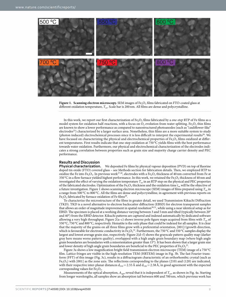
Results and DiscussionPhysical characterization. We deposited Fe films by physical vapour deposition (PVD) on top of fluorine doped tin oxide (FTO) covered glass – see Methods section for fabrication details. Then, we employed RTP to oxidize the Fe into Fe2O3. In previous work27,28, electrodes with a Fe2O3 thickness of 40 nm converted from Fe at 350 °C in a flow furnace yielded highest performance. In this work, we retained the Fe2O3 thickness of 40 nm and investigated the effect of varying the oxidation temperature Tox in an RTP step on the physical and PEC properties of the fabricated electrodes. Optimization of the Fe2O3 thickness and the oxidation time tox will be the objective of a future investigation. Figure 1 shows scanning electron microscope (SEM) images of films prepared using Tox in a range from 500 °C to 800 °C. All the films are dense and polycrystalline, in agreement with previous reports on Fe2O3 fabricated by furnace oxidation of Fe films29.
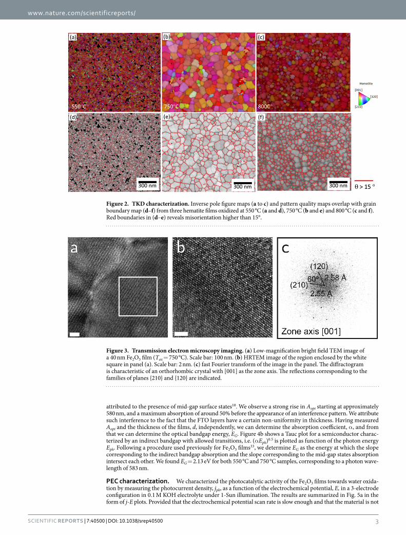
To characterize the microstructure of the films in greater detail, we used Transmission Kikuchi Diffraction (TKD). TKD is a novel alternative to electron backscatter diffraction (EBSD) for electron transparent samples that allows an order of magnitude improvement in spatial resolution30,31, while using a near identical setup as for EBSD. The specimen is placed at a working distance varying between 3 and 5 mm and tilted (typically between 20° and 40°) from the EBSD detector. Kikuchi patterns are captured and indexed automatically by dedicated software allowing a very high throughput. Figure 2(a–c) shows inverse pole figure maps acquired from films with Tox of 550 °C, 750 °C and 800 °C, respectively. Hematite is the only phase that could be indexed for all samples. It is clear that the majority of the grains on all three films grow with a preferential orientation, [001]//growth direction, which is favourable for electronic conductivity in Fe2O3
32. Furthermore, the 750 °C and 550 °C samples display the largest and lowest average grain size, respectively. Figure 2(d–f) shows the grayscale pattern quality map (darker gray here means worse pattern quality), overlapped with a high angle grain boundary map (where high angle grain boundaries are boundaries with a misorientation greater than 15°). It has been shown that a larger grain size and lower density of high angle grain boundaries are beneficial to the PEC properties of Fe2O3
25.Figure 3a shows a low magnification bright field transmission electron microscope (TEM) image of a 750 °C
film. Lattice fringes are visible in the high resolution TEM (HRTEM) image in Fig. 3b. The fast Fourier trans-form (FFT) of this image (Fig. 3c), results in a diffractogram characteristic of an orthorhombic crystal (such as Fe2O3) with [001] as the zone axis. The reflections corresponding to the planes (210) and (120) are indicated, with their respective inter-planar distances d210 = 2.55 Å and d120 = 2.58 Å, in good agreement with the expected corresponding values for Fe2O3.
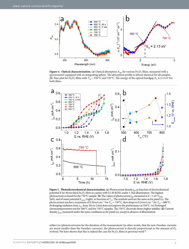
Measurements of the optical absorption, Aopt, reveal that it is independent of Tox, as shown in Fig. 4a. Starting from longer wavelengths, all samples show an absorption tail between 600 and 700 nm, which previous work has
Figure 1. Scanning electron microscopy. SEM images of Fe2O3 films fabricated on FTO-coated glass at different oxidation temperature, Tox. Scale bar is 200 nm. All films are dense and polycrystalline.
www.nature.com/scientificreports/
3Scientific RepoRts | 7:40500 | DOI: 10.1038/srep40500
attributed to the presence of mid-gap surface states10. We observe a strong rise in Aopt starting at approximately 580 nm, and a maximum absorption of around 50% before the appearance of an interference pattern. We attribute such interference to the fact that the FTO layers have a certain non-uniformity in thickness. Having measured Aopt and the thickness of the films, d, independently, we can determine the absorption coefficient, α , and from that we can determine the optical bandgap energy, EG. Figure 4b shows a Tauc plot for a semiconductor charac-terized by an indirect bandgap with allowed transitions, i.e. (α Eph)0.5 is plotted as function of the photon energy Eph. Following a procedure used previously for Fe2O3 films33, we determine EG as the energy at which the slope corresponding to the indirect bandgap absorption and the slope corresponding to the mid-gap states absorption intersect each other. We found EG = 2.13 eV for both 550 °C and 750 °C samples, corresponding to a photon wave-length of 583 nm.
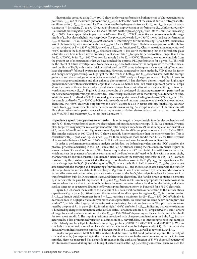
PEC characterization. We characterized the photocatalytic activity of the Fe2O3 films towards water oxida-tion by measuring the photocurrent density, jph, as a function of the electrochemical potential, E, in a 3-electrode configuration in 0.1 M KOH electrolyte under 1-Sun illumination. The results are summarized in Fig. 5a in the form of j-E plots. Provided that the electrochemical potential scan rate is slow enough and that the material is not
Figure 2. TKD characterization. Inverse pole figure maps (a to c) and pattern quality maps overlap with grain boundary map (d–f) from three hematite films oxidized at 550 °C (a and d), 750 °C (b and e) and 800 °C (c and f). Red boundaries in (d–e) reveals misorientation higher than 15°.
Figure 3. Transmission electron microscopy imaging. (a) Low-magnification bright field TEM image of a 40 nm Fe2O3 film (Tox = 750 °C). Scale bar: 100 nm. (b) HRTEM image of the region enclosed by the white square in panel (a). Scale bar: 2 nm. (c) fast Fourier transform of the image in the panel. The diffractogram is characteristic of an orthorhombic crystal with [001] as the zone axis. The reflections corresponding to the families of planes {210} and {120} are indicated.
www.nature.com/scientificreports/
4Scientific RepoRts | 7:40500 | DOI: 10.1038/srep40500
subject to (photo)corrosion for the duration of the measurement (in other words, that the non-Faradaic currents are much smaller than the Faradaic currents), the photocurrent is directly proportional to the amount of O2 evolved. We have shown that this is indeed the case for Fe2O3 films in previous work34.
Figure 4. Optical characterization. (a) Optical absorption Aopt for various Fe2O3 films, measured with a spectrometer equipped with an integrating sphere. The absorption profile is almost identical for all samples. (b) Tauc plot for Fe2O3 films with Tox = 550 °C and 750 °C. The energy of the optical bandgap EG is 2.13 eV for both films.
Figure 5. Photoelectrochemical characterization. (a) Photocurrent density jph as function of electrochemical potential E for 40 nm thick Fe2O3 films in contact with 0.1 M KOH, under 1-Sun illumination. The highest photoactivity is found for the 750 °C sample. (b) The values of photocurrent jph measured at E = 1.45 VRHE (left), and of onset potential Eonset (right), as function of Tox. The symbols used are the same as for panel (a). The photocurrent reaches a maximum of 0.56 mA cm−2 for Tox = 750 °C, then drops to 0.24 mA cm−2 for Tox = 800 °C. Prolonging oxidation time, tox, from 30 s to 2 min does not improve the performance at 550 °C. (c) Prolonged chronoamperometry test for 500 °C and for 750 °C samples. The 750 °C electrode shows higher stability. (d) Current density jdark measured under the same conditions as for panel (a), except in absence of illumination.
www.nature.com/scientificreports/
5Scientific RepoRts | 7:40500 | DOI: 10.1038/srep40500
Photoanodes prepared using Tox = 500 °C show the lowest performance, both in terms of photocurrent onset potential, Eonset and of maximum photocurrent, jmax, (i.e., before the onset of the current due to electrolysis with-out illumination). Eonset, is around 1.4 V vs. the reversible hydrogen electrode (RHE), and jmax is approximately 0.4 mA cm−2. Increasing Tox to 550 °C causes a substantial improvement in performance. Eonset shifts cathodically (i.e. towards more negative potentials) by about 300 mV. Neither prolonging tox from 30 s to 2 min, nor increasing Tox to 600 °C has an appreciable impact on the j-E curve. For Tox = 700 °C, we notice an improvement in the mag-nitude of jph, but also a slightly less steep slope. The photoanode with Tox = 750 °C shows the best performance: Eonset of around 1.1 V vs. RHE and jmax of 0.6 mA cm−2. Interestingly, further increasing Tox to 800 °C results in a loss of photoactivity, with an anodic shift of Eonset to 1.3 V vs. RHE. Figure 5b shows a comparison of the photo-current achieved at E = 1.45 V vs. RHE, as well as of Eonset, as function of Tox. Clearly, an oxidation temperature of 750 °C results in the highest value of jph, close to 0.6 mA cm−2. It is worth mentioning that the borosilicate glass substrates used here suffered severe cracking if kept at a certain Tox for specific periods of time; longer than 2 min for Tox < 700 °C, 5 s for Tox < 800 °C or even for merely 2 s for Tox = 800 °C. Therefore, we cannot conclude from the present set of measurements that we have reached the optimal PEC performance for a given Tox. This will be the object of future investigations. Nonetheless, a jph close to 0.6 mA cm−2 is comparable to the value meas-ured on films of Fe2O3 with similar thickness fabricated on FTO using techniques such as sputtering35 or atomic layer deposition36 followed by furnace annealing. However, compared to these methods, RTP allows for faster and energy-saving processing. We highlight that the trends in both jph and Eonset are consistent with the average grain size and density of grain boundaries as revealed by TKD analysis. Larger grain size in Fe2O3 is known to reduce charge recombination and thus enhance photocurrent7. It has also been demonstrated that high angle grain boundaries (with misorientation larger than 15°, as also defined here) can cause significant potential drops along the z-axis of the electrodes, which results in a stronger bias required to initiate water splitting, or in other words a more anodic Eonset
25. Figure 5c shows the results of a prolonged chronoamperometry test performed on the best and worst performing photoelectrodes. Here, we kept E constant while monitoring jph as function of time. While the sample oxidized at 500 °C shows a degradation of performance leading to a loss of 35% of jph after 12 h, the sample oxidized at Tox = 750 °C stabilizes within one hour and remains constant over the whole measurement. Therefore, the 750 °C electrode outperforms the 500 °C electrode also in terms stability. Finally, Fig. 5d show results from jdark measurements under the same conditions as for Fig. 5a, except in absence of illumination. All films show rather similar performance when acting as water oxidation electrocatalysts, with a current onset above 1.65 V vs. RHE and maximum jdark of less than 0.1 mA cm−2.
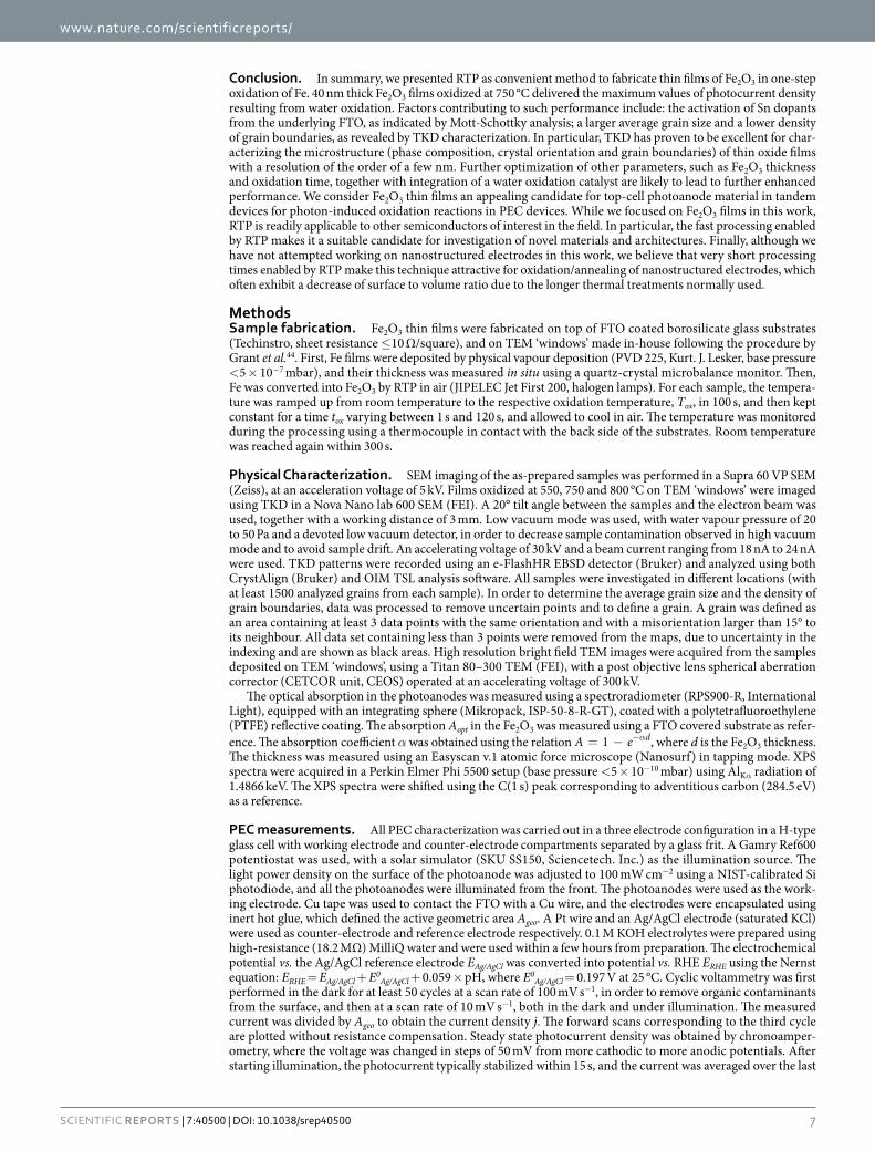
Impedance spectroscopy measurements. In order to gain a deeper insight into the electrochemistry of our Fe2O3 films, we performed extensive electrochemical impedance spectroscopy (EIS). We obtained Nyquist plots (negative imaginary vs. real component of the total complex impedance Z) for all samples at various values of E, under 1-Sun illumination. Figure 6a shows Nyquist plots for different photoanodes at E = 1.16 V vs. RHE. The samples oxidized at 500 °C and 800 °C show a notably higher impedance than the other electrodes. This is consistent with j-E profile of Fig. 5a, since Eonset for these samples is more anodic than 1.16 V vs. RHE. Nyquist plots recorded between 1.76 V and 0.76 V vs. RHE for all measured samples are shown in Figure S4.
In order to perform more quantitative analysis on this data, we defined equivalent circuits (ECs) based on the physical processes occurring in the Fe2O3 and at the Fe2O3/interface during the PEC measurements. Figure 6b shows the two ECs used in this work: The Hamann equivalent circuit36 used to fit plots with two semi-circles, which indicate the presence of two time constants; and the Randle circuit37 used to fit plots with one semi-circle, characterized by one time constant. The Hamann circuit contains the following elements: the FTO-Fe2O3 contact resistance, RS; the resistance associated with charge recombination losses in the Fe2O3, Rtrap; the capacitance of the space-charge layer in Fe2O3 (i.e. of the region of Fe2O3 where the built-in field is present), Cbulk; the capacitance associated with the charging and discharging of surface states, CSS; and the resistance associated with the transfer of charges from the surface states to the electrolyte, RSS. This EC was first introduced by Hamann and co-workers to describe water oxidation taking place via surface states at the Fe2O3/electrolyte interface, i.e. holes are first transferred from bulk Fe2O3 to surface states, and then to the electrolyte. The Randle circuit contains 3 elements: RS in series with the parallel impedance of Cbulk and Rtrap. Such an EC is more appropriate for a water oxidation process where there is direct transfer of holes from the semiconductor valence band to the electrolyte, and where surface states act as spectators. Examples of Nyquist plots fitting are shown in Figure S5 for a 750 °C electrode.
Figure 6(c–e) shows the results of the analysis of EIS data. First, we turn our attention to the surface states capacitance CSS in panel (c). We observed the same trend for all samples: for a given Tox, CSS is close to zero for E < Eonset; then, it quickly increases from E = Eonset, reaching a maximum for E = Eonset + 150–200 mV; finally, it decreases back to negligible values for yet more anodic potentials. We observed the same behaviour in previous studies38,39, which is the fingerprint for water oxidation taking place via surface states. This picture is corrobo-rated by the plot of RSS in panel (b): RSS is rather high (≥ 104 Ω cm2) for E < Eonset, indicating that water oxidation is hindered by charge recombination at the surface states. For a more anodic E, RSS drops between 3 and 4 orders of magnitude and reaches a minimum for E = Eonset + 150–200 mV depending on the electrode, and it levels off for even more anodic E. The trapping resistance associated with charge recombination in the bulk, Rtrap, is char-acterized by a less pronounced variation as a function of E. Nevertheless, it is interesting to note that samples with relatively similar j-E plots also have similar Rtrap profiles (550/600 °C, 700/750 °C, and 500/800 °C). We can conclude that water oxidation takes place via surface states for all samples independently of Tox. Furthermore, the data analysis indicates a strong correlation between trends in Eonset and CSS, as well as between jph and RSS.
Finally, we performed Mott-Schottky analysis to determine the flat band potential, Efb, and the density of charge donors Nd (corresponding to the charge carrier concentration in the semiconductor in the dark) for two samples. Here, we measured Z at a specific frequency in the dark as a function of E. We chose a frequency of 104 Hz, in order to avoid filling and un-filling of surface states at the Fe2O3/electrolyte interface. Then, we used the
www.nature.com/scientificreports/
6Scientific RepoRts | 7:40500 | DOI: 10.1038/srep40500
Randle EC to extract values of Cbulk as function of E. The following relation for Cbulk can be derived from electro-static considerations38:
ε ε= × − −A C N E E k T e( / ) (2/ ) ( / )bulk r d fb B2
0
where A is the area of the electrode exposed to the electrolyte, ε0 is the permittivity of vacuum, εr is the dielectric constant of the semiconductor, e is the elementary electronic charge, kB is the Boltzmann constant and T is the absolute temperature. We used here the same geometric area Ageo we had previously used to determine j. We deter-mined Nd and Efb from the slope and from the intersection of the (Ageo/Cbulk)2 vs. E plot with the horizontal axis, respectively. The slope corresponding to the 750 °C electrode is much less steep than that of the 550 °C electrode, denoting a higher Nd. In fact, the increase in Nd is striking, more than an order of magnitude: from 6.1 × 10¹⁹ to 7.23 × 1020 cm−3. While the former value is characteristic of Fe2O3 with a negligible amount of external impurities and where the major source of conduction electrons is oxygen vacancies40, the latter value is typical of Fe2O3 sam-ples with external impurities acting as electron donors41. Several reports have described an improvement in water oxidation photocurrent on Fe2O3 upon doping with elements with higher valence than Fe, for instance Ti, Si and Sn42. In particular, it has been shown that for sufficiently high temperatures (typically between 725 °C and 750 °C) Sn diffuses out of FTO and into the Fe2O3, thus doping the latter and enhancing the photocurrent43. Indeed, XPS measurements confirmed the diffusion of Sn from FTO into Fe2O3 for Tox = 750 °C, while this was not the case for Tox = 550 °C (see Figure S6). We conclude that an oxidation temperature of 750 °C is sufficient to incorporate Sn in the Fe2O3 film. We therefore ascribe the enhancement of jph upon increasing Tox from 550 °C to 750 °C to the combination of increased average grain size and higher majority charge carrier concentration. Finally, the 800 °C electrode shows a worse photoresponse than the 750 °C one in terms of both Eonset and jph, despite a yet higher Tox, as mentioned earlier. We identified two likely mechanisms for the lower jph. First, the average grain size is smaller, as evidenced by TKD analysis. Second, the FTO- Fe2O3 contact resistance RS is increased, as shown in Figure S7, which results in a lower electron conductivity in the electrode. Furthermore, we can ascribe the more anodic Eonset to the higher density of high angle grain boundaries, which is once again clear from TKD analysis.
From the Mott-Schottky plots we also concluded that Efb is slightly lower for the 750 °C sample than for the 550 °C sample (0.45 V and 0.51 V vs. RHE, respectively). The similar values of Efb indicate that the amplitude of the built-in field in Fe2O3 is hardly affected by Tox. Further confirmation that the thermodynamics of the solid/liquid junction is to a large extent independent of Tox comes from open circuit measurements both in the dark and under illumination, from which we determined that the photovoltage sustained by Fe2O3, Eph, is around 0.25 V for all samples (see Figure S8). While such a value is comparable with what has been recorded on other model systems based on Fe2O3 thin films14, it is considerably smaller than the magnitude of the optical bandgap, which highlights that there is substantial room for improvement.
Figure 6. Impedance spectroscopy characterization. (a) Nyquist plots for Fe2O3 electrodes with different Tox, in contact with 0.1 M KOH, under 1-Sun illumination, at E = 1.16 VRHE. (b) Equivalent circuits used to fit the EIS data. Top: the Hamann equivalent circuit used to fit Nyquist plots with two time constants. Bottom: the Randle circuit used to fit plots with one time constant. Panels (c–f) show results from the data fitting. (c) Surface states capacitance, CSS. (d) Trapping resistance Rtrap. (e) Charge transfer resistance RSS. (f) Mott-Schottky analysis performed on the 550 °C and 750 °C samples.
www.nature.com/scientificreports/
7Scientific RepoRts | 7:40500 | DOI: 10.1038/srep40500
Conclusion. In summary, we presented RTP as convenient method to fabricate thin films of Fe2O3 in one-step oxidation of Fe. 40 nm thick Fe2O3 films oxidized at 750 °C delivered the maximum values of photocurrent density resulting from water oxidation. Factors contributing to such performance include: the activation of Sn dopants from the underlying FTO, as indicated by Mott-Schottky analysis; a larger average grain size and a lower density of grain boundaries, as revealed by TKD characterization. In particular, TKD has proven to be excellent for char-acterizing the microstructure (phase composition, crystal orientation and grain boundaries) of thin oxide films with a resolution of the order of a few nm. Further optimization of other parameters, such as Fe2O3 thickness and oxidation time, together with integration of a water oxidation catalyst are likely to lead to further enhanced performance. We consider Fe2O3 thin films an appealing candidate for top-cell photoanode material in tandem devices for photon-induced oxidation reactions in PEC devices. While we focused on Fe2O3 films in this work, RTP is readily applicable to other semiconductors of interest in the field. In particular, the fast processing enabled by RTP makes it a suitable candidate for investigation of novel materials and architectures. Finally, although we have not attempted working on nanostructured electrodes in this work, we believe that very short processing times enabled by RTP make this technique attractive for oxidation/annealing of nanostructured electrodes, which often exhibit a decrease of surface to volume ratio due to the longer thermal treatments normally used.
MethodsSample fabrication. Fe2O3 thin films were fabricated on top of FTO coated borosilicate glass substrates (Techinstro, sheet resistance ≤ 10 Ω/square), and on TEM ‘windows’ made in-house following the procedure by Grant et al.44. First, Fe films were deposited by physical vapour deposition (PVD 225, Kurt. J. Lesker, base pressure < 5 × 10⁻⁷ mbar), and their thickness was measured in situ using a quartz-crystal microbalance monitor. Then, Fe was converted into Fe2O3 by RTP in air (JIPELEC Jet First 200, halogen lamps). For each sample, the tempera-ture was ramped up from room temperature to the respective oxidation temperature, Tox, in 100 s, and then kept constant for a time tox varying between 1 s and 120 s, and allowed to cool in air. The temperature was monitored during the processing using a thermocouple in contact with the back side of the substrates. Room temperature was reached again within 300 s.
Physical Characterization. SEM imaging of the as-prepared samples was performed in a Supra 60 VP SEM (Zeiss), at an acceleration voltage of 5 kV. Films oxidized at 550, 750 and 800 °C on TEM ‘windows’ were imaged using TKD in a Nova Nano lab 600 SEM (FEI). A 20° tilt angle between the samples and the electron beam was used, together with a working distance of 3 mm. Low vacuum mode was used, with water vapour pressure of 20 to 50 Pa and a devoted low vacuum detector, in order to decrease sample contamination observed in high vacuum mode and to avoid sample drift. An accelerating voltage of 30 kV and a beam current ranging from 18 nA to 24 nA were used. TKD patterns were recorded using an e-FlashHR EBSD detector (Bruker) and analyzed using both CrystAlign (Bruker) and OIM TSL analysis software. All samples were investigated in different locations (with at least 1500 analyzed grains from each sample). In order to determine the average grain size and the density of grain boundaries, data was processed to remove uncertain points and to define a grain. A grain was defined as an area containing at least 3 data points with the same orientation and with a misorientation larger than 15° to its neighbour. All data set containing less than 3 points were removed from the maps, due to uncertainty in the indexing and are shown as black areas. High resolution bright field TEM images were acquired from the samples deposited on TEM ‘windows’, using a Titan 80–300 TEM (FEI), with a post objective lens spherical aberration corrector (CETCOR unit, CEOS) operated at an accelerating voltage of 300 kV.
The optical absorption in the photoanodes was measured using a spectroradiometer (RPS900-R, International Light), equipped with an integrating sphere (Mikropack, ISP-50-8-R-GT), coated with a polytetrafluoroethylene (PTFE) reflective coating. The absorption Aopt in the Fe2O3 was measured using a FTO covered substrate as refer-ence. The absorption coefficient α was obtained using the relation = − α−A e1 d, where d is the Fe2O3 thickness. The thickness was measured using an Easyscan v.1 atomic force microscope (Nanosurf) in tapping mode. XPS spectra were acquired in a Perkin Elmer Phi 5500 setup (base pressure < 5 × 10⁻¹⁰ mbar) using AlKα radiation of 1.4866 keV. The XPS spectra were shifted using the C(1 s) peak corresponding to adventitious carbon (284.5 eV) as a reference.
PEC measurements. All PEC characterization was carried out in a three electrode configuration in a H-type glass cell with working electrode and counter-electrode compartments separated by a glass frit. A Gamry Ref600 potentiostat was used, with a solar simulator (SKU SS150, Sciencetech. Inc.) as the illumination source. The light power density on the surface of the photoanode was adjusted to 100 mW cm−2 using a NIST-calibrated Si photodiode, and all the photoanodes were illuminated from the front. The photoanodes were used as the work-ing electrode. Cu tape was used to contact the FTO with a Cu wire, and the electrodes were encapsulated using inert hot glue, which defined the active geometric area Ageo. A Pt wire and an Ag/AgCl electrode (saturated KCl) were used as counter-electrode and reference electrode respectively. 0.1 M KOH electrolytes were prepared using high-resistance (18.2 MΩ) MilliQ water and were used within a few hours from preparation. The electrochemical potential vs. the Ag/AgCl reference electrode EAg/AgCl was converted into potential vs. RHE ERHE using the Nernst equation: ERHE = EAg/AgCl + E0
Ag/AgCl + 0.059 × pH, where E0Ag/AgCl = 0.197 V at 25 °C. Cyclic voltammetry was first
performed in the dark for at least 50 cycles at a scan rate of 100 mV s−1, in order to remove organic contaminants from the surface, and then at a scan rate of 10 mV s−1, both in the dark and under illumination. The measured current was divided by Ageo to obtain the current density j. The forward scans corresponding to the third cycle are plotted without resistance compensation. Steady state photocurrent density was obtained by chronoamper-ometry, where the voltage was changed in steps of 50 mV from more cathodic to more anodic potentials. After starting illumination, the photocurrent typically stabilized within 15 s, and the current was averaged over the last

www.nature.com/scientificreports/
8Scientific RepoRts | 7:40500 | DOI: 10.1038/srep40500
20 s of the measurement. Open circuit voltage data was recorded for at least 20 min, both in the dark and under illumination, in order to ensure stabilization of the semiconductor/electrolyte interface. For the EIS measure-ments, the DC voltage was changed in steps of 50 mV from 1.76 VRHE and 0.46 VRHE, to avoid polarization effects. An AC voltage with root mean square amplitude of 10 mV and frequency varying between 105 Hz and 0.1 Hz was superimposed to the DC bias. Nyquist plots obtained under illumination were fitted using the software Echem Analyst (Gamry). Mott-Schottky analysis was performed in between 1.76 VRHE and 0.46 VRHE, with an AC voltage with a fixed frequency of 104 Hz.
References1. Armaroli, N. & Balzani, V. The future of energy supply: Challenges and opportunities. Angewandte Chemie - International Edition
46, 52–66 (2007).2. Vesborg, P. C. K. & Jaramillo, T. F. Addressing the terawatt challenge: scalability in the supply of chemical elements for renewable
energy. RSC Adv. 2, 7933 (2012).3. Herron, J. A., Kim, J., Upadhye, A. A., Huber, G. W. & Maravelias, C. T. A general framework for the assessment of solar fuel
technologies. Energy Environ. Sci. 8, 126–157 (2015).4. Shen, J. et al. Electrocatalytic reduction of carbon dioxide to carbon monoxide and methane at an immobilized cobalt
protoporphyrin. Nat. Commun. 6, 8177 (2015).5. Lan, R., Irvine, J. T. S. & Tao, S. Synthesis of ammonia directly from air and water at ambient temperature and pressure. Sci. Rep. 3,
Article number: 1145 (2013).6. Hellman, A., Iandolo, B., Wickman, B., Grönbeck, H. & Baltrusaitis, J. Electro-oxidation of water on hematite: Effects of surface
termination and oxygen vacancies investigated by first-principles. Surf. Sci. 640, 45–49 (2015).7. Sivula, K., Le Formal, F. & Grätzel, M. Solar water splitting: progress using hematite (α -Fe2O3 ) photoelectrodes. ChemSusChem 4,
432–49 (2011).8. Young, K. M. H., Klahr, B. M., Zandi, O. & Hamann, T. W. Photocatalytic water oxidation with hematite electrodes. Catal. Sci.
Technol. 3, 1660 (2013).9. Iandolo, B., Wickman, B., Zorić, I. & Hellman, A. The rise of hematite: origin and strategies to reduce the high onset potential for the
oxygen evolution reaction. J. Mater. Chem. A 3, 16896–16912 (2015).10. Marusak, L. A., Messier, R. & White, W. B. Optical absorption spectrum of hematite, α -Fe2O3 near IR to UV. J. Phys. Chem. Solids
41, 981–984 (1980).11. Katz, M. J. et al. Toward solar fuels: Water splitting with sunlight and ‘rust’? Coord. Chem. Rev. 256, 2521–2529 (2012).12. Yeh, L.-S. R. Iron Oxide Semiconductor Electrodes in Photoassisted Electrolysis of Water. J. Electrochem. Soc. 124, 833 (1977).13. Hamann, T. W. Splitting water with rust: hematite photoelectrochemistry. Dalton Trans. 41, 7830–4 (2012).14. Du, C. et al. Hematite-based water splitting with low turn-on voltages. Angew. Chemie - Int. Ed. 52, 12692–12695 (2013).15. Liu, Y. et al. Synergistic Effect of Surface Plasmonic particles and Surface Passivation layer on ZnO Nanorods Array for Improved
Photoelectrochemical Water Splitting. Sci. Rep. 6, 29907 (2016).16. Lin, Y., Yuan, G., Sheehan, S., Zhou, S. & Wang, D. Hematite-based solar water splitting: challenges and opportunities. Energy
Environ. Sci. 4, 4862 (2011).17. Roozeboom, F. Rapid thermal processing systems: A review with emphasis on temperature control. J. Vac. Sci. Technol. B
Microelectron. Nanom. Struct. 8, 1249 (1990).18. Hart, M. J. & Evans, A. G. R. Rapid thermal processing in semiconductor technology. Semicond. Sci. Technol. 3, 421–436 (1988).19. Borisenko, V. E. & Hesketh, P. J. Rapid Thermal Processing of Semiconductors. doi: 10.1007/978-1-4899-1804-8 (Springer US, 1997).20. Nulman, J., Krusius, J. P. & Gat, A. Rapid thermal processing of thin gate dielectrics. Oxidation of silicon. IEEE Electron Device Lett.
6, 205–207 (1985).21. Greiner, M. E. & Gibbons, J. F. Diffusion of silicon in gallium arsenide using rapid thermal processing: Experiment and model. Appl.
Phys. Lett. 44, 750 (1984).22. Rohatgi, A., Chen, Z., Doshi, P., Pham, T. & Ruby, D. High-efficiency silicon solar cells by rapid thermal processing. Appl. Phys. Lett.
65, 2087 (1994).23. Lovelett, R. J., Hanket, G. M., Shafarman, W. N., Birkmire, R. W. & Ogunnaike, B. A. Design and experimental implementation of an
effective control system for thin film Cu(InGa)Se2 production via rapid thermal processing. J. Process Control 46, 24–33 (2016).24. Tate, T. J. et al. Crystal regrowth of YBCO thin films by ion implantation and rapid thermal annealing. Phys. C Supercond. 235–240,
569–570 (1994).25. Warren, S. C. et al. Identifying champion nanostructures for solar water-splitting. Nat. Mater. 12, 842–9 (2013).26. Iandolo, B. et al. Correlating flat band and onset potentials for solar water splitting on model hematite photoanodes. RSC Adv. 5,
61021–61030 (2015).27. Iandolo, B., Antosiewicz, T. J., Hellman, A. & Zorić, I. On the mechanism for nanoplasmonic enhancement of photon to electron
conversion in nanoparticle sensitized hematite films. Phys. Chem. Chem. Phys. 15, 4947–54 (2013).28. Iandolo, B. & Zäch, M. Enhanced water splitting on thin-film hematite photoanodes functionalized with lithographically fabricated
Au nanoparticles. Aust. J. Chem. 65, 633–637 (2012).29. Hiralal, P. et al. Nanostructured hematite photoelectrochemical electrodes prepared by the low temperature thermal oxidation of
iron. Sol. Energy Mater. Sol. Cells 95, 1819–1825 (2011).30. Geiss, R., Keller, R., Sitzman, S. & Rice, P. New Method of Transmission Electron Diffraction to Characterize Nanomaterials in the
SEM. Microsc. Microanal. 17, 386–387 (2011).31. Keller, R. R. & Geiss, R. H. Transmission EBSD from 10 nm domains in a scanning electron microscope. J. Microsc. 245, 245–251
(2012).32. Iordanova, N., Dupuis, M. & Rosso, K. M. Charge transport in metal oxides: A theoretical study of hematite α -Fe2O3. J. Chem. Phys.
122, 144305 (2005).33. Misho, R. H. & Murad, W. A. Band gap measurements in thin films of hematite Fe2O3, pyrite FeS2 and troilite FeS prepared by
chemical spray pyrolysis. Sol. Energy Mater. Sol. Cells 27, 335–345 (1992).34. Iandolo, B. et al. Faradaic efficiency of O2 evolution on metal nanoparticle sensitized hematite photoanodes. Phys. Chem. Chem.
Phys. 16, 1271–5 (2014).35. Jia, L., Harbauer, K., Bogdanoff, P., Ellmer, K. & Fiechter, S. Sputtering Deposition of Ultra-thin α -Fe2O3 Films for Solar Water
Splitting. J. Mater. Sci. Technol. 31, 655–659 (2015).36. Klahr, B., Gimenez, S., Fabregat-Santiago, F., Hamann, T. & Bisquert, J. Water oxidation at hematite photoelectrodes: The role of
surface states. J. Am. Chem. Soc. 134, 4294–4302 (2012).37. Randles, J. E. B. Kinetics of rapid electrode reactions. Discuss. Faraday Soc. 1, 11 (1947).38. Iandolo, B. & Hellman, A. The role of surface states in the oxygen evolution reaction on hematite. Angew. Chemie - Int. Ed. 53,
13404–13408 (2014).39. Iandolo, B., Wickman, B., Svensson, E., Paulsson, D. & Hellman, A. Tailoring Charge Recombination in Photoelectrodes Using
Oxide Nanostructures. Nano Lett. 16, 2381–2386 (2016).

www.nature.com/scientificreports/
9Scientific RepoRts | 7:40500 | DOI: 10.1038/srep40500
40. Kumar, B. et al. Photochemical and Photoelectrochemical Reduction of CO2. Annu. Rev. Phys. Chem. 63, 541–569 (2012).41. Barroso, M., Pendlebury, S. R., Cowan, A. J. & Durrant, J. R. Charge carrier trapping, recombination and transfer in hematite (α -
Fe2O3) water splitting photoanodes. Chem. Sci. 4, 2724 (2013).42. Tamirat, A. G., Rick, J., Dubale, A. A., Su, W.-N. & Hwang, B.-J. Using hematite for photoelectrochemical water splitting: a review of
current progress and challenges. Nanoscale Horiz. 1, 243–267 (2016).43. Ling, Y. & Li, Y. Review of Sn-Doped Hematite Nanostructures for Photoelectrochemical Water Splitting. Part. Part. Syst. Charact.
31, 1113–1121 (2014).44. Grant, A. W., Hu, Q.-H. & Kasemo, B. Transmission electron microscopy windows for nanofabricated structures. Nanotechnology
15, 1175–1181 (2004).
AcknowledgementsThe research leading to these results has received funding from the People Programme (Marie Curie Actions) of the European Union’s Seventh Framework Programme (FP7/2007-2013) under REA Grant Agreement No. 609405 (COFUNDPostdocDTU). B.W. and A.H. thank Formas (project number 245-2014-1478) for financial support. B.I. thanks Dowon Bae for the assistance with the optical measurements.
Author ContributionsB.I., B.W. and A.H. designed the experiments. B.I. and B.W. fabricated the samples. B.I. performed the TEM, SEM, AFM and PEC characterization. A.B.F. performed the TKD imaging and analysis. B.W. performed the XPS characterization. B.I. wrote the first draft of the manuscript. All authors contributed to the final version of the manuscript.
Additional InformationSupplementary information accompanies this paper at http://www.nature.com/srepCompeting financial interests: The authors declare no competing financial interests.How to cite this article: Wickman, B. et al. Iron Oxide Films Prepared by Rapid Thermal Processing for Solar Energy Conversion. Sci. Rep. 7, 40500; doi: 10.1038/srep40500 (2017).Publisher's note: Springer Nature remains neutral with regard to jurisdictional claims in published maps and institutional affiliations.
This work is licensed under a Creative Commons Attribution 4.0 International License. The images or other third party material in this article are included in the article’s Creative Commons license,
unless indicated otherwise in the credit line; if the material is not included under the Creative Commons license, users will need to obtain permission from the license holder to reproduce the material. To view a copy of this license, visit http://creativecommons.org/licenses/by/4.0/ © The Author(s) 2017