by cephas e. small - university of...
TRANSCRIPT
1
INVERTED ORGANIC ELECTRONIC AND OPTOELECTRONIC DEVICES
By
CEPHAS E. SMALL
A DISSERTATION PRESENTED TO THE GRADUATE SCHOOL OF THE UNIVERSITY OF FLORIDA IN PARTIAL FULFILLMENT
OF THE REQUIREMENTS FOR THE DEGREE OF DOCTOR OF PHILOSOPHY
UNIVERSITY OF FLORIDA
2012

2
© 2012 Cephas E. Small

3
To my parents

4
ACKNOWLEDGMENTS
First of all, I give all praise to my Lord and Savior, Jesus Christ, who has guided
my life and has continually opened doors of opportunity for me to walk through. I
continue to put Him first and look forward to the new things that He will do in my life.
There are a number of people who I must thank for their contributions to my
graduate studies and to this dissertation work. It starts with my PhD advisor, Dr. Franky
So. From the very beginning, Dr. So showed a willingness and a desire to have me join
his research group. When I joined the group in 2006, I was this energetic, enthusiastic
graduate student that knew nothing about organic electronics. Believing that I could be
successful, Dr. So set high expectations for my work and was patient with me
throughout the entire process. He has showed me, through his own example, the level
of hard work, focus, and dedication that it takes to contribute to the research work at a
high level. I have become a better researcher and am better equipped to have success
in the next stage in my career as a result of his guidance. Although my years working
with him has been very challenging, I am grateful for everything he has taught me. I
would also like to thank Dr. Norton, Dr. Pearton, Dr. Xue, and Dr. Rinzler for serving on
my committee and providing feedback concerning my research.
I would also like to acknowledge several of the past and present members of Dr.
So's research group: Dr. Kaushik Roy Choudury, Dr. Jegadesan Subbiah, Dr. DoYoung
Kim, Dr. Stephen Tsang, Dr. Leo Cheung, Dr. Neetu Chopra, Dr. Jaewon Lee, Dr. Dong
Woo Song, Dr. Galileo Sarasqueta, Alok Gupta, Frederick Steffy, Mikail Shaikh, Nikhil
Bhandari, Pieter De Somer, Verena Giese, Song Chen, Michael Hartel, Jesse Manders,
Tzung Han Lai, Sujin Baek, Lordania Constantinou, and Eric Klump. I thank these
wonderful people for not only contributing to my research work, but also serving as an

5
extended family that has contributed to my growth and development. In addition, I thank
Dr. Mikhail Noginov, Dr. Carl Bonner, Dr. Suely Black, and the rest of the faculty and
staff at Norfolk State University's Center for Materials Research. I thank them for giving
me the opportunity to conduct basic research for the first time. It was at NSU that I
discovered my passion for research and science.
Lastly, I thank my family, who has continuously supported me in my academic
endeavors and has helped me to stay grounded in my faith. Their love was all the
motivation I would need to finish what I started.
6
TABLE OF CONTENTS
page
ACKNOWLEDGMENTS .................................................................................................. 4
LIST OF TABLES ............................................................................................................ 8
LIST OF FIGURES .......................................................................................................... 9
ABSTRACT ................................................................................................................... 13
CHAPTER
1 INTRODUCTION .................................................................................................... 15
1.1 Organic Semiconductors ................................................................................... 15
1.1.1 Classes of Organic Semiconductors........................................................ 15 1.1.2 Advantages and Disadvantages .............................................................. 16
1.2 Charge Transport and Injection in Organic Semiconductors ............................. 18
1.2.1 Charge Transport .................................................................................... 18 1.2.2 Charge Injection ...................................................................................... 19
1.3 Inverted Organic Electronic Devices ................................................................. 20 1.3.1 Organic Light-Emitting Diodes (OLEDs) .................................................. 20 1.3.2 Organic Photovoltaics (OPVs) ................................................................. 21
1.4 Dissertation Outline........................................................................................... 22
2 ELECTRON ACCEPTING INTERLAYERS AS SELECTIVE p-CONTACTS FOR INVERTED ORGANIC ELECTRONIC DEVICES ................................................... 27
2.1 Introductory Remarks ........................................................................................ 27
2.2 Experimental Details ......................................................................................... 31 2.2.1 Device Fabrication ................................................................................... 31 2.2.2 Device Characterization .......................................................................... 32
2.3 Results and Discussions ................................................................................... 34 2.3.1 J-V Characterization ................................................................................ 34
2.3.2 DI-SCLC Transient Measurement ........................................................... 35
2.3.3 MoO3-doped NPB Injection Layer For Improved Hole Injection ............... 36
2.4 Concluding Remarks ......................................................................................... 39
3 INTRODUCTION TO ORGANIC PHOTOVOLTAIC CELLS ................................... 50
3.1 Overview and History ........................................................................................ 50 3.2 Principles of Operation ...................................................................................... 53 3.3 Photovoltaic Cell Characterization .................................................................... 54
3.3.1 Current-Voltage Measurement ................................................................ 55 3.3.2 Spectral Response Measurement ........................................................... 55

7
3.4 Progress in Organic Photovoltaic Cell Performance ......................................... 57
3.4.1 Novel Conjugated Polymers for OPVs..................................................... 58 3.4.2 Inverted Device Geometry ....................................................................... 60
4 HIGH EFFICIENCY INVERTED POLYMER PHOTOVOLTAIC CELLS .................. 67
4.1 Introductory Remarks ........................................................................................ 67 4.2 Experimental Details ......................................................................................... 70
4.2.1 Device Fabrication ................................................................................... 70 4.2.2 Device Characterization .......................................................................... 71
4.3 Results and Discussions ................................................................................... 71 4.3.1 ZnO-PVP Nanocomposite Film Characterization .................................... 71 4.3.2 Inverted Polymer Photovoltaic Cell with ZnO-PVP Nanocomposite
ETL ............................................................................................................... 74 4.3 Concluding Remarks ......................................................................................... 78
5 LOSS MECHANISMS IN THICK-FILM LOW-BANDAP POLYMER SOLAR CELLS .................................................................................................................... 89
5.1 Introductory Remarks ........................................................................................ 89
5.2 Experimental Details ......................................................................................... 92 5.2.1 Device Fabrication ................................................................................... 92 5.2.2 Device Characterization .......................................................................... 93
5.3 Results and Discussions ................................................................................... 93 5.3.1 PDTG-TPD:PC71BM Solar Cell Performance .......................................... 93
5.3.2 Loss Mechanisms in Thick-Film PDTG-TPD:PC71BM Solar Cells ........... 97 5.4 Concluding Remarks ....................................................................................... 106
6 CONCLUSIONS ................................................................................................... 120
LIST OF REFERENCES ............................................................................................. 122
BIOGRAPHICAL SKETCH .......................................................................................... 136
8
LIST OF TABLES
Table page 4-1 Average solar cell performance for inverted PDTG-TPD:PC71BM devices with
5, 10, 20, or 30-minute UV-ozone treated ZnO-PVP composite ETLs under initial AM 1.5G solar illumination. ........................................................................ 79
5-1 Averaged solar cell performance for inverted PDTG-TPD:PC71BM devices with various active layer thickness under initial AM 1.5G solar illumination. ..... 107
5-2 Averaged solar cell performance for inverted P3HT:PC61BM devices with various active layer thickness under initial AM 1.5G solar illumination. ............ 107

9
LIST OF FIGURES
Figure page 1-1 Number of scientific publications contributing to the topics "organic
photovoltaics" and "organic light emitting diodes". ............................................. 24
1-2 Large-scale roll-to-roll manufacturing process for flexible organic electronic devices. .............................................................................................................. 24
1-3 Schematic energy diagram of a metal-organic semiconductor interface with an interface dipole formed at the interface. ........................................................ 25
1-4 Commercially available products based high-resolution OLED display technology. ......................................................................................................... 25
1-5 Comparison between a bottom-emitting and top-emitting OLED with a conventional or inverted structure. ...................................................................... 26
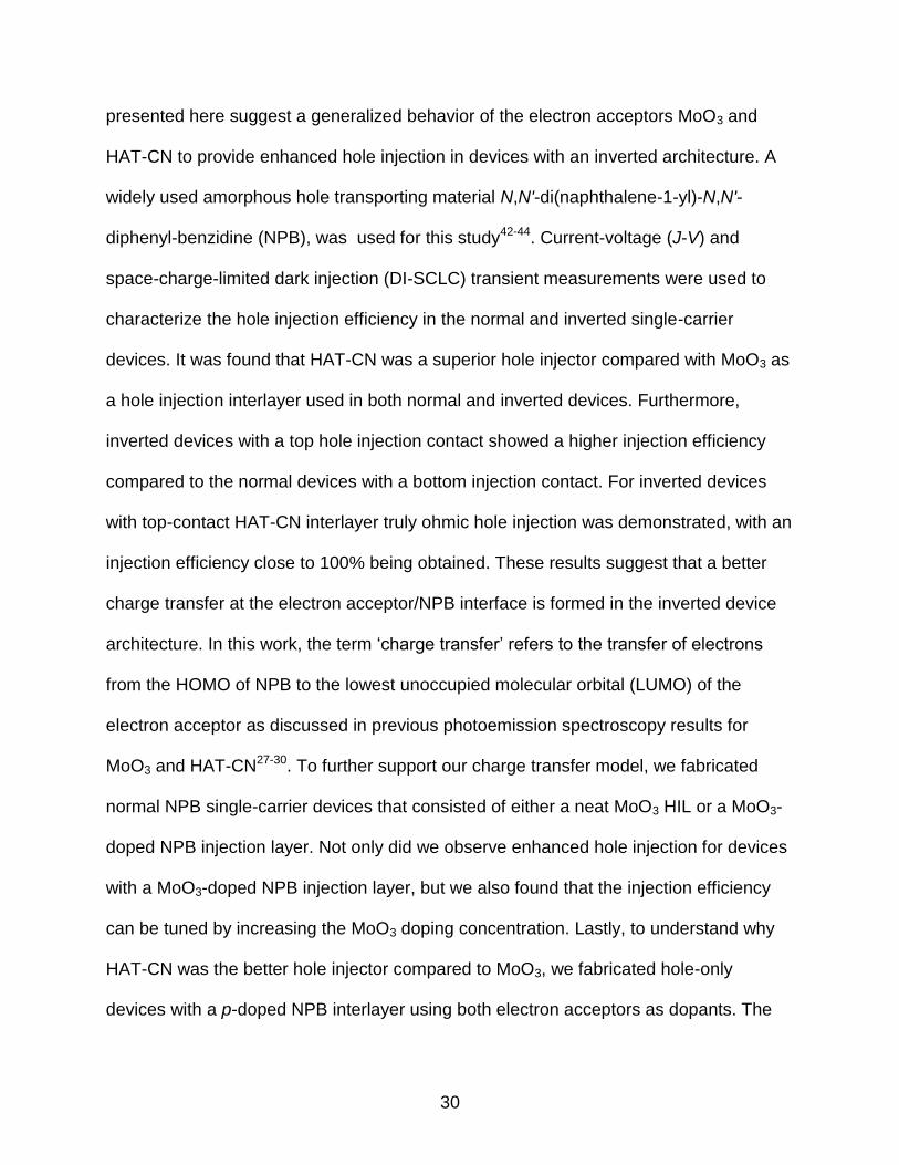
2-1 Molecular structure of electron acceptors and conducting polymers used as injection layers in conventional OLEDs. ............................................................. 41
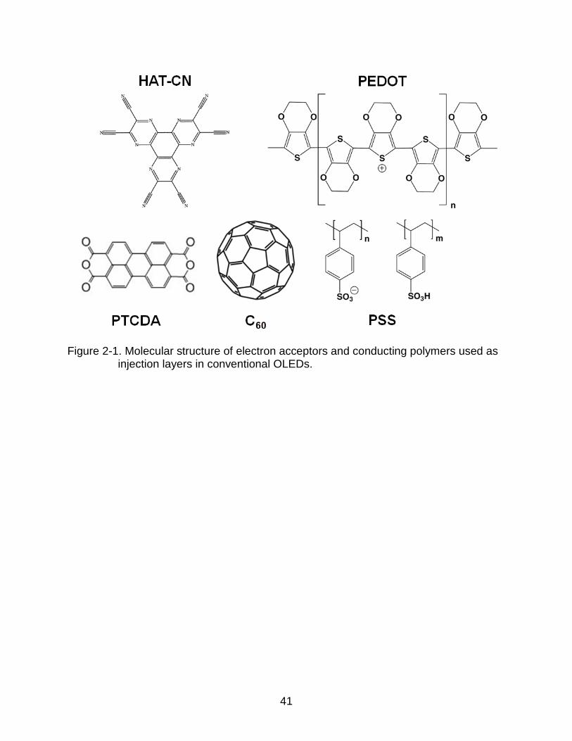
2-2 Energy level diagram at the NPB/HAT-CN/Au interface. .................................... 42
2-3 Schematic cross-section view of NPB single-carrier devices fabricated in this study. .................................................................................................................. 43
2-4 An ideal DI-SCLC transient current response for a trap-free organic semiconductor. ................................................................................................... 43
2-5 Current density and injection efficiency vs. electric field for conventional and inverted NPB hole-only devices using MoO3 or HAT-CN as HIL. ....................... 44
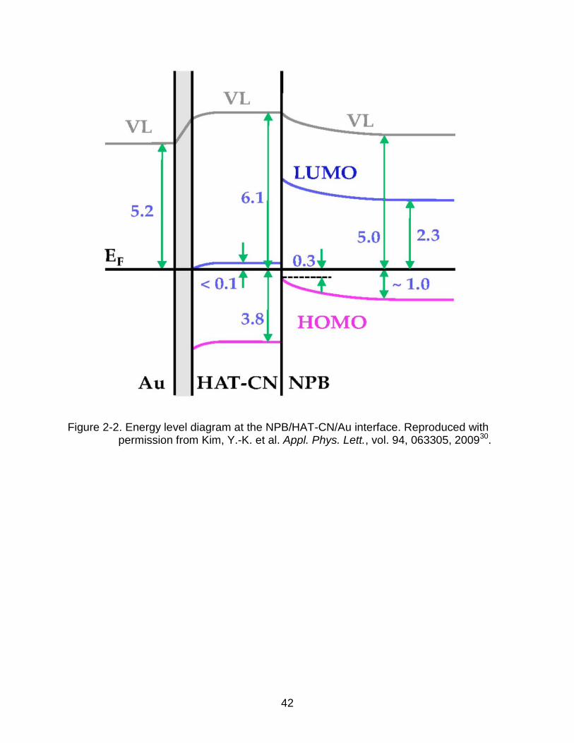
2-6 DI-current density transients measured at various applied voltages using MoO3 as HIL. ...................................................................................................... 45
2-7 DI-current density transients measured at various applied voltages using HAT-CN as HIL. .................................................................................................. 46
2-8 Injection efficiency, η, extracted from DI-SCLC transient current measurements vs. electric field for normal and inverted NPB single-carrier devices with either MoO3 or HAT-CN as injection layer. ..................................... 47
2-9 Hole mobility (µDI) as a function of electric field (F1/2) for normal and inverted NPB hole-only devices with either MoO3 or HAT-CN injection layer. ................. 47
10
2-10 Current density and injection efficiency plots for conventional NPB hole-only devices with either a neat MoO3 or MoO3-doped NPB HIL of varying doping concentration (1, 5, 10 mol%). ............................................................................ 48
2-11 Current density vs. applied electric field for MoO3–doped and HAT-CN–doped NPB single-carrier devices. ..................................................................... 49
2-12 Current density vs. electric field for normal NPB single-carrier devices with either ITO or Au anode. ...................................................................................... 49
3-1 Schematic illustrations for various solution processing methods used in the fabrication of large-scale and laboratory-scale polymer photovoltaic cells. ........ 62
3-2 Schematic diagram illustrating an organic donor-acceptor heterjunction, as well as the bilayer and bulk heterojunction concepts. ......................................... 62
3-3 Typical J-V characteristics for a photovoltaic cell tested in the dark (JD) and under illumination (JL). ........................................................................................ 63
3-4 Chemical structure for standard electron donor and acceptor materials used in the fabrication of organic photovoltaic cells. ................................................... 64
3-5 Schematic illustration showing the molecular orbital hybridization for a donor-acceptor (D-A) copolymer and the resulting reduction in the effective bandgap. ............................................................................................................ 65
3-6 Chemical structure for state-of-the-art donor-acceptor copolymers used for high efficiency polymer photovoltaic cells. .......................................................... 65
3-7 Normal vs. inverted device architectures for organic photovoltaic cells. ............. 66
4-1 The normal and inverted device geometries for P3HT:PCBM solar cells. .......... 79
4-2 An illustration of the process and the six processing steps employed during fabrication of the R2R coated modules. .............................................................. 80
4-3 AFM image (measuring 5 × 5 µm2) of a knife-over-edge coated ZnO nanoparticle film used in the fabrication of large-scale R2R-processed modules. ............................................................................................................. 80
4-4 Tapping mode AFM images for as-prepared and 10-min UV-ozone treated ZnO-PVP nanocomposite films. .......................................................................... 81
4-5 Tapping-mode AFM phase images for ZnO-PVP nanocomposite films before and after UV-ozone treatment (5 µm scale size). ............................................... 82
4-6 X-ray photoemission spectra (XPS) for the as-prepared and 10-minute UV-ozone treated ZnO-PVP nanocomposite films. ................................................... 83

11
4-7 UV-visible-NIR transmission spectra for the as-prepared and 10-minute UV-ozone treated ZnO-PVP nanocomposite films. ................................................... 84
4-8 Photo J-V characteristics for inverted PDTG-TPD:PC71BM solar cells highlighting the effect of prolonged light soaking on device performance under AM 1.5G solar illumination at 100 mW cm-2. ............................................ 84
4-9 Photo J-V characteristics and EQE spectra for inverted PDTG-TPD:PC71BM solar cells with UV-ozone treated ZnO-PVP nanocomposite ETL for various treatment times. .................................................................................................. 85
4-10 Dark J-V characteristics for inverted PDTG-TPD:PC71BM solar cells with UV-ozone treated ZnO-PVP nanocomposite ETL measured as-is and after being light soaked using either a 600 nm or 350 nm band-pass filter. ......................... 86
4-11 Certified I-V characteristics for an inverted PDTG-TPD:PC71BM solar cell with 10-minute UV-ozone treated ZnO-PVP nanocomposite ETL. The device was certified by NEWPORT Corporation. .................................................................. 87
4-12 Solar cell parameters versus time for encapsulated inverted PDTG-TPD:PC71BM with as-prepared and 10-minute UV-ozone treated ZnO-PVP nanocomposite ETLs. ......................................................................................... 88
5-1 Device structure for PDTG-TPD:PC71BM solar cells, P3HT:PC61BM solar cells, and corresponding single-carrier devices studied in this work. ................ 108
5-2 Photo J-V characteristics and EQE spectra for inverted PDTG-TPD:PC71BM solar cells with increasing active layer thickness. ............................................. 109
5-3 Photo J-V characteristics and EQE spectra for inverted P3HT:PC61BM solar cells with increasing active layer thickness. ...................................................... 110
5-4 Average fill factor and EQE versus active layer thickness for PDTG-TPD:PC71BM and P3HT:PC61BM solar cells. ................................................... 111
5-5 Current density times active layer thickness (J × L) versus electric field curves for PDTG-TPD:PC71BM hole-only devices with 100 nm and 409 nm-thick layers........................................................................................................ 112
5-6 Field-dependent EQE spectra for PDTG-TPD:PC71BM solar cells with increasing active layer thickness. ..................................................................... 113
5-7 Normalized photocurrent density (JL) as a function of internal electric field for inverted PDTG-TPD:PC71BM solar cells with increasing active layer thickness. ......................................................................................................... 114
5-8 UV-Vis-NIR spectra and fraction of photons absorbed vs. active layer thickness for PDTG-TPD:PC71BM and P3HT:PC61BM solar cells. ................... 115

12
5-9 Normalized Jph−Veff curves for under 100 mW cm-2 illumination for the devices studied. ................................................................................................ 116
5-10 Light intensity dependence of the photocurrent and fill factor for 105 nm-thick and 409 m-thick PDTG-TPD:PC71BM solar cells. ............................................. 117
5-11 Calculated number of photons absorbed in the PDTG-TPD:PC71BM layer under AM1.5G illumination and photocurrent loss as a function of layer thickness. ......................................................................................................... 118
5-12 The critical active layer thickness corresponding to the onset of SCL photocurrent (Lc) in low bandgap polymer solar cells versus bandgap of the polymer. ............................................................................................................ 119

13
Abstract of Dissertation Presented to the Graduate School of the University of Florida in Partial Fulfillment of the Requirements for the Degree of Doctor of Philosophy
INVERTED ORGANIC ELECTRONIC AND OPTOELECTRONIC DEVICES
By
Cephas E. Small
December 2012
Chair: Franky So Major: Materials Science and Engineering
The research and development of organic electronics for commercial application
has received much attention due to the unique properties of organic semiconductors
and the potential for low-cost high-throughput manufacturing. For improved large-scale
processing compatibility and enhanced device stability, an inverted geometry has been
employed for devices such as organic light emitting diodes and organic photovoltaic
cells. These improvements are attributed to the added flexibility to incorporate more air-
stable materials into the inverted device geometry. However, early work on organic
electronic devices with an inverted geometry typically showed reduced device
performance compared to devices with a conventional structure.
In the case of organic light emitting diodes, inverted devices typically show high
operating voltages due to insufficient carrier injection. Here, a method for enhancing
hole injection in inverted organic electronic devices is presented. By incorporating an
electron accepting interlayer into the inverted device, a substantial enhancement in hole
injection efficiency was observed as compared to conventional devices. Through a
detailed carrier injection study, it is determined that the injection efficiency

14
enhancements in the inverted devices are due to enhanced charge transfer at the
electron acceptor/organic semiconductor interface.
A similar situation is observed for organic photovoltaic cells, in which devices with
an inverted geometry show limited carrier extraction in early studies. In this work,
enhanced carrier extraction is demonstrated for inverted polymer solar cells using a
surface-modified ZnO-polymer composite electron-transporting layer. The insulating
polymer in the composite layer inhibited aggregation of the ZnO nanoparticles, while the
surface-modification of the composite interlayer improved the electronic coupling with
the photoactive layer. As a result, inverted polymer solar cells with power conversion
efficiencies of over 8% were obtained. To further study carrier extraction in inverted
polymer solar cells, the active layer thickness dependence of the efficiency was
investigated. For devices with active layer thickness < 200 nm, power conversion
efficiencies over 8% was obtained. This result is important for demonstrating improved
large-scale processing compatibility. Above 200 nm, significant reduction in cell
efficiency were observed. A detailed study of the loss processes that contributed to the
reduction in efficiency for thick-film devices are presented.

15
CHAPTER 1 INTRODUCTION
1.1 Organic Semiconductors
Although research focused on the use of organic semiconductors for electronic
and optoelectronic application started as a mere academic curiosity, today low-cost
commercially-viable technology based on these novel materials have become a reality.
Rapid progress in the field of organic electronics and optoelectronics is in large part due
to do the significant research contributions from academia, research laboratories and
industry. As an example, the number of scientific publications contributing to the
subjects 'organic photovoltaic cells' and 'organic light emitting diodes' by year, which is
displayed in Figure 1-1, clearly highlights the significant increase in contributions for
these research areas per year. Initially, the interest in organic electronics and
optoelectronics was aimed at studying conjugated molecules that exhibited interesting
electrical and optical properties. Development of these novel organic semiconductors
has continued to be a core focus of the research. This chapter will introduce the reader
to organic semiconductors: the different classes of these materials, their properties, and
the use of these materials in optoelectronic devices. Lastly, the research scope for this
dissertation will be presented.
1.1.1 Classes of Organic Semiconductors
Organic semiconductors can be categorized into two classes: small molecular-
weight molecules and conjugated polymers. Small molecules are discrete units with
several to a few hundred atoms. Consequently, the molecular weight for these materials
are well-defined. Organic small-molecules are typically processed at high vacuum by
thermal evaporation/sublimation for thin-film fabrication. By controlling the substrate

16
heating temperature during processing, amorphous, polycrystalline, and single-crystal
small molecule thin films can be produced. Due to their ease of processing and the
diverse electrical and optical properties of these materials, organic small molecules
have been used as hole-transporting, electron transporting, and photoactive materials in
organic thin-film transistors (OTFTs), organic light-emitting diodes (OLEDs) and organic
photovoltaics (OPVs).
In contrast to organic small molecules, conjugated polymers have a molecular
structure consisting of long chains of repeat units called monomers. The molecular
weights for conjugated polymers are typically very large and vary from polymer to
polymer. These materials are processed from solution using various processing
methods such as spin coating, drop casting, or ink-jet printing. The use of solution
processing permits the control of numerous processing conditions that impact the thin-
film morphology, such as the choice of solvent and annealing conditions. However, the
solution processing of organic layer stacks can be difficult due to the requirement of
orthogonal solvents for the organic layers. Controlling the morphology of solution-
processed polymer films and developing novel solution-processing procedures for
fabricating organic layer stacks is still a subject of ongoing research and is critical for
various device applications.
1.1.2 Advantages and Disadvantages
Organic semiconductors, due to their intrinsic properties, has many advantages
that are suitable for electronic and optoelectronic applications. For one, organic
semiconductors have a low material cost and can be processed using low-cost
fabrication methods. For example, high vacuum thermal evaporation of small molecules
is a simple process that is more energy efficient than processing methods using for thin-

17
film inorganic semiconductors, such as sputtering and plasma-enhanced chemical
vapor deposition (PECVD). The cost for fabrication is reduced even further when
solution processing methods are employed. These low-cost fabrication methods are
compatible with large-scale roll-to-roll (R2R) manufacturing on rigid or flexible
substrates, allowing organic-based devices to be produced at high throughput. Figure 1-
2 shows the large-scale manufacture of flexible organic electronics produced by
different parties. Another key advantage to organic semiconductors is the ability to
tailor the properties of these material through intelligent chemical modification. This has
lead to increased charge carrier mobility in OTFTs, efficient color tuning OLEDs, and
enhanced light harvesting in OPVs.
Interestingly, the intrinsic properties of organic semiconductors also introduce a
number of disadvantages that hinder the performance of electronic and optoelectronic
devices. These materials have much lower carrier mobilities and intrinsic carrier
concentrations compared to inorganic semiconductors. Consequently, the device
performance of organic electronic and optoelectronic devices becomes limited by the
low electrical conductivity of organic semiconductors. Another issue is the inability to
obtain high purity levels in organic materials. As a result, a high trap density due to
impurities and structural defects is common for organic semiconductors. Lastly, organic
materials degrade in ambient condition due to oxidation and exposure to moisture. To
produce devices with enhanced stability and lifetime, it becomes necessary to design
suitable encapsulation technology. This adds additional complexity to the fabrication of
organic electronic devices.

18
1.2 Charge Transport and Injection in Organic Semiconductors
1.2.1 Charge Transport
The transport of electrons and holes in organic solids can be described by three
different models based on either a microscopic or macroscopic view of charge
conduction. In the microscopic view, charge carrier hop between adjacent molecules to
facilitate charge transport. In this hopping model, the charge hopping rate is a function
of the reorganization energy () and the electron coupling factor (Vab)1. If and Vab are
known, the diffusion coefficient ( ) can be calculated as
(1-1)
where is the hopping distance. The carrier mobility can then be estimated from the
Einstein relation:
(1-2)
where is electron charge, is the Boltzmann constant, and is the absolute
temperature.
In the macroscopic view, charge conduction occurs by drift via an external field
along disordered hopping sites in the organic semiconductor. For this charge transport
model, first proposed by Poole and Frenkel, the field-dependent carrier mobility is given
as
(1-3)
where is the Poole-Frenkel slope, is the zero field mobility, is the
electric field, and is the dielectric constant. The Poole-Frenkel model has been widely
used to experimentally determine carrier mobilities in organic semiconductors and is

19
employed in Chapter 2 to quantify carrier mobility for the hole transporting materials
studied in that work.
Another charge transport model worth mentioning is the Gaussian disorder model
(GDM), which assumes that the transport energy states in the organic semiconductor
have a Gaussian distribution. Since the charge hopping in this model is field-assisted
and thermally activated in the disordered system, the carrier mobility is a function of
electric field, temperature, and energetic and positional disorder2. The energetic
disorder can be conceptualized as the width of the Gaussian distribution, while the
positional disorder is the geometric randomness cause by structural defects3.
1.2.2 Charge Injection
Figure 1-3 shows the energy diagram for a metal-organic semiconductor interface
based on the Mott-Schottky model4. When an organic semiconductor is in contact with a
metal, an energy barrier is formed at the organic semiconductor-metal interface. The
energy barriers for electron and hole injection ( , ) are determined by the electron
affinity ( ), the ionization potential ( ), and the vacuum level shift due to the formation
of an interface dipole ( ):
(1-4)
(1-5)
where is the metal work function. Reducing the electron and hole energy barriers to
carrier injection is critically important to the efficient operation of OLEDs. However, this
can be a challenge since the work function of the metal electrode typically does not
match the transport level of interest for the organic semiconductor. Novel approaches
for reducing the energy barrier include introducing interlayers between the metal and
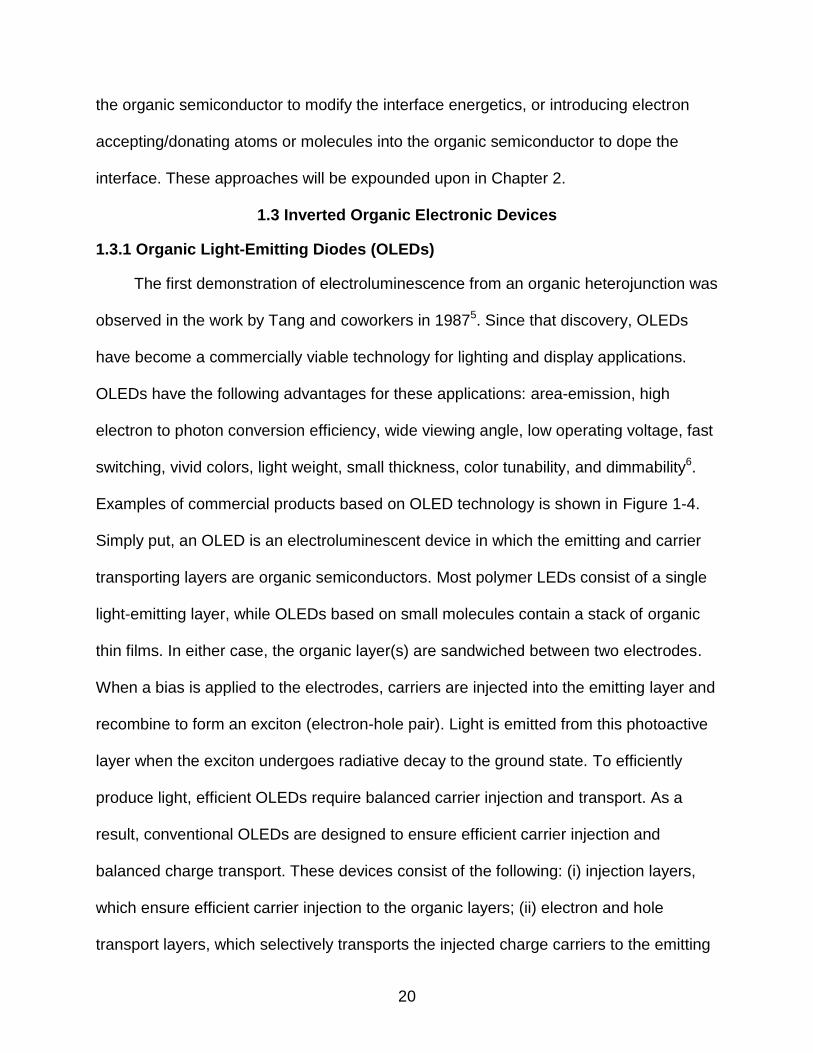
20
the organic semiconductor to modify the interface energetics, or introducing electron
accepting/donating atoms or molecules into the organic semiconductor to dope the
interface. These approaches will be expounded upon in Chapter 2.
1.3 Inverted Organic Electronic Devices
1.3.1 Organic Light-Emitting Diodes (OLEDs)
The first demonstration of electroluminescence from an organic heterojunction was
observed in the work by Tang and coworkers in 19875. Since that discovery, OLEDs
have become a commercially viable technology for lighting and display applications.
OLEDs have the following advantages for these applications: area-emission, high
electron to photon conversion efficiency, wide viewing angle, low operating voltage, fast
switching, vivid colors, light weight, small thickness, color tunability, and dimmability6.
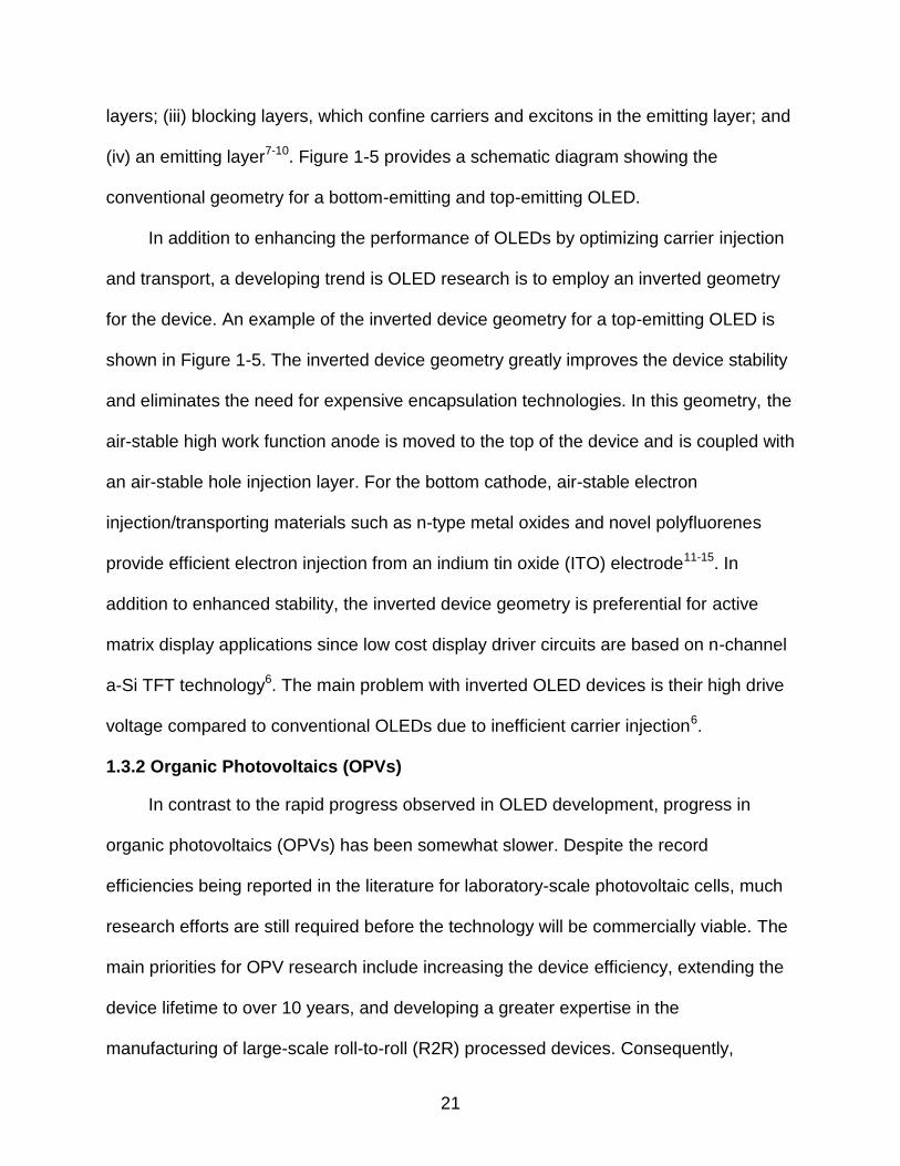
Examples of commercial products based on OLED technology is shown in Figure 1-4.
Simply put, an OLED is an electroluminescent device in which the emitting and carrier
transporting layers are organic semiconductors. Most polymer LEDs consist of a single
light-emitting layer, while OLEDs based on small molecules contain a stack of organic
thin films. In either case, the organic layer(s) are sandwiched between two electrodes.
When a bias is applied to the electrodes, carriers are injected into the emitting layer and
recombine to form an exciton (electron-hole pair). Light is emitted from this photoactive
layer when the exciton undergoes radiative decay to the ground state. To efficiently
produce light, efficient OLEDs require balanced carrier injection and transport. As a
result, conventional OLEDs are designed to ensure efficient carrier injection and
balanced charge transport. These devices consist of the following: (i) injection layers,
which ensure efficient carrier injection to the organic layers; (ii) electron and hole
transport layers, which selectively transports the injected charge carriers to the emitting
21
layers; (iii) blocking layers, which confine carriers and excitons in the emitting layer; and
(iv) an emitting layer7-10. Figure 1-5 provides a schematic diagram showing the
conventional geometry for a bottom-emitting and top-emitting OLED.
In addition to enhancing the performance of OLEDs by optimizing carrier injection
and transport, a developing trend is OLED research is to employ an inverted geometry
for the device. An example of the inverted device geometry for a top-emitting OLED is
shown in Figure 1-5. The inverted device geometry greatly improves the device stability
and eliminates the need for expensive encapsulation technologies. In this geometry, the
air-stable high work function anode is moved to the top of the device and is coupled with
an air-stable hole injection layer. For the bottom cathode, air-stable electron
injection/transporting materials such as n-type metal oxides and novel polyfluorenes
provide efficient electron injection from an indium tin oxide (ITO) electrode11-15. In
addition to enhanced stability, the inverted device geometry is preferential for active
matrix display applications since low cost display driver circuits are based on n-channel
a-Si TFT technology6. The main problem with inverted OLED devices is their high drive
voltage compared to conventional OLEDs due to inefficient carrier injection6.
1.3.2 Organic Photovoltaics (OPVs)
In contrast to the rapid progress observed in OLED development, progress in
organic photovoltaics (OPVs) has been somewhat slower. Despite the record
efficiencies being reported in the literature for laboratory-scale photovoltaic cells, much
research efforts are still required before the technology will be commercially viable. The
main priorities for OPV research include increasing the device efficiency, extending the
device lifetime to over 10 years, and developing a greater expertise in the
manufacturing of large-scale roll-to-roll (R2R) processed devices. Consequently,

22
researchers worldwide have attempted to enhance cell efficiency through employing
novel material design and device concepts. Furthermore, improving device stability by
developing more effective encapsulation technology and investigating the issues
involved in manufacturing large-scale OPV modules have become a focus of the work.
Interestingly, employing an inverted device geometry for OPV cells has lead to
enhanced cell efficiency, increased device stability, and improved R2R processing
compatibility. A more detailed introduction to organic photovoltaic cells will be provided
in Chapter 4.
1.4 Dissertation Outline
There are two main topics presented in this dissertation. First, a method for
enhancing carrier injection in inverted organic electronic devices is presented. This
result is of critical importance for OLEDs, since reducing the drive voltage of inverted
devices is required for display applications. In the second, the factors affecting carrier
extraction are determined for inverted polymer photovoltaic cells. In Chapter 1, the
reader is presented a general introduction to organic electronics. This chapter describes
the properties of organic semiconductors, discusses models used to describe charge
carrier transport and injection in these materials, and highlights the motivation behind
using the inverted device geometry for organic electronic devices. In Chapter 2, a
detailed study of carrier injection in inverted organic electronic devices using electron
accepting interlayers is presented. In addition to demonstrating ohmic hole injection in
inverted devices, the origin of this enhanced hole injection is experimentally
investigated.
The subsequent chapters of this dissertation focuses on inverted organic
photovoltaic cells. Chapter 3 provides an introduction to organic photovoltaics,

23
describing the history, operating principles, and experimental methods used to
characterize photovoltaic cells. Furthermore, recent process in this research field is
discussed, including the use of the inverted device geometry. In Chapter 4, high
efficiency inverted polymer photovoltaic cells are demonstrated. By incorporating a
ZnO-polymer composite film as the electron transporting layer, enhanced charge
collection is observed in the devices. Using the same device geometry, the thickness
dependence of the efficiency is investigated in Chapter 5. The loss processes
responsible for limited device performance in inverted polymer solar cells with thick
active layer are investigated. A theoretical model designed to help explain the role that
space-charge effects play in increasing photocurrent loss is presented. Finally, Chapter
6 summarizes the results of this work and provides a brief outlook on future work.

24
Figure 1-1. Number of scientific publications contributing to the topics "organic
photovoltaics" and "organic light emitting diodes". Search done through ISI, Web of Science database.
Figure 1-2. Large-scale roll-to-roll manufacturing process for flexible organic electronic
devices16,17.
25
Figure 1-3. Schematic energy diagram of a metal-organic semiconductor interface with an interface dipole formed at the interface1.
Figure 1-4. Commercially available products based high-resolution OLED display technology18.

26
Figure 1-5. Comparison between a bottom-emitting and top-emitting OLED with a conventional or inverted structure. A) Bottom-emitting OLED with conventional structure. B) Top-emitting OLED with a conventional structure. C) Top-emitting OLED with an inverted structure. HTL = hole transport layer, EBL = electron blocking layer, EML = emission layer, HBL = hole blocking layer, ETL = electron transport layer, CL = capping layer6.
27
CHAPTER 2 ELECTRON ACCEPTING INTERLAYERS AS SELECTIVE P-CONTACTS FOR
INVERTED ORGANIC ELECTRONIC DEVICES
2.1 Introductory Remarks
Research aimed at optimizing the performance of organic light-emitting diodes
(OLEDs) has received much attention in recent years due to the enormous potential of
the technology in flat panel display and solid state lighting applications19. A key
requirement to demonstrating OLEDs with efficient operation is to optimize carrier
injection from the electrodes to the active emitting layer20,21. As discussed in Chapter 1,
this requirement is due to the low intrinsic carrier concentration of organic
semiconductors and thus the need to reduce the device operating voltage. Optimizing
carrier injection is not a simple task, especially since OLEDs utilize wide band-gap
materials whose energy levels do not match the work-function of the electrodes. The
work function mismatch is especially a problem for hole injection because the work
function of transparent electrodes such as indium tin oxide (ITO) is less than 5.0 eV
while the highest occupied molecular orbital (HOMO) energies of wide band-gap hole
transporting materials commonly used in OLEDs are typically 5.5 eV or higher, resulting
in low hole injection efficiencies.
To overcome this limitation, interlayers are often incorporated into the device to
enhance hole injection. Figure 2-1 shows the molecular structure for materials
commonly used as hole injection layers in conventional OLEDs. In general, these
materials can be grouped into two categories. One class of materials used for the hole
injecting interlayer is conducting polymers, such as poly(3,4-ethylene-dioxythiophene)
poly(styrenesulfonate) (PEDOT:PSS)22-24. Although the use of PEDOT:PSS as a hole
injection layer (HIL) has been quite popular in small-molecule and polymer OLED

28
research, its work-function of 5.0 eV is not adequate to provide optimum hole injection
into wide band-gap materials with a deep HOMO energy25. Another class of materials
used as interlayer is strong electron acceptors. These materials can facilitate enhanced
hole injection in OLEDs26. Unlike conducting polymer HILs, electron accepting
interlayers modify the energy levels of the anode and wide band-gap hole transporting
materials when inserted between these two layers. Previously reported ultraviolet
photoemission spectroscopy (UPS) results showed that the electron accepting interlayer
was responsible for both the large vacuum level shift in the anode, whether indium tin
oxide (ITO) or Au, and the observed band-bending in the HOMO level of the hole-
transporting layer27-30. As an illustration, Figure 2-2 shows the schematic energy level
alignment of the Au/HAT-CN/NPB interface based on in situ ultraviolet photoemission
spectroscopy (UPS) measurements. The strong band-bending of the hole-transporting
layer’s HOMO level is indicative that the Fermi level moves down and pins at a certain
position as typical for p-doping. The use of electron acceptors for controlled p-doping in
amorphous hole-transporting materials employed in high efficiency OLEDs has been
well studied31-37. For example, strong p-type doping has also been observed when
MoO3 was used as a dopant in hole transporters with a deep HOMO level36. Due to their
ability to modify the energy levels of the anode and the wide band-gap hole transporting
layers, these electron acceptors can serve as efficient hole injectors for wide band-gap
materials with a deep HOMO level.
Despite the use of conducting polymers or electron acceptors as interlayers for
improved carrier injection in organic devices, truly ohmic hole injection has rarely been
reported. When the hole injection contact is ohmic, the carrier transport is limited by the

29
bulk of the materials rather than the injection contact. As a result of the ohmic injection,
the carrier transport is space-charge limited32. The determination between bulk-limited
versus injection-limited transport is made by calculating the carrier injection efficiency,
which is the ratio between the measured steady-state current density of the device and
the theoretical space-charge-limited current density given by the Mott-Gurney Law38.
Even for conventional bottom-injection contact hole-only devices with PEDOT:PSS as
an interlayer, injection-limited transport and low injection efficiency values ranging from
30 to 60% have been reported25. Additional studies featuring MoO3 as an electron
accepting interlayers have reported even lower injection efficiencies for similar single-
carrier devices39. Recently, two novel approaches have been demonstrated for
achieving ohmic hole injection in OLEDs. One approach is to utilize a composite HIL
consisting of a mixture of conducting polymers with different work functions and
graphene for ohmic hole injection in flexible OLEDs40. The other approach for achieving
ohmic hole injection consists of using electron accepting interlayers in OLEDs with an
inverted architecture, with a substantial enhancement in current density being observed
in the device when the bottom hole injection contact using PEDOT:PSS interlayer is
replaced by a top hole injection contact using MoO3 interlayer41. In these inverted
devices, the electron accepting interlayer is deposited on top of the hole transporting
layer to form the top hole injection contact. Using this approach, optimized hole injection
into wide band-gap materials can be achieved. However, the origin of this enhancement
is not understood.
The mechanism of enhanced hole injection in inverted organic devices with
different electron accepting interlayers is investigated in this chapter. The results
30
presented here suggest a generalized behavior of the electron acceptors MoO3 and
HAT-CN to provide enhanced hole injection in devices with an inverted architecture. A
widely used amorphous hole transporting material N,N'-di(naphthalene-1-yl)-N,N'-
diphenyl-benzidine (NPB), was used for this study42-44. Current-voltage (J-V) and
space-charge-limited dark injection (DI-SCLC) transient measurements were used to
characterize the hole injection efficiency in the normal and inverted single-carrier
devices. It was found that HAT-CN was a superior hole injector compared with MoO3 as
a hole injection interlayer used in both normal and inverted devices. Furthermore,
inverted devices with a top hole injection contact showed a higher injection efficiency
compared to the normal devices with a bottom injection contact. For inverted devices
with top-contact HAT-CN interlayer truly ohmic hole injection was demonstrated, with an
injection efficiency close to 100% being obtained. These results suggest that a better
charge transfer at the electron acceptor/NPB interface is formed in the inverted device
architecture. In this work, the term ‘charge transfer’ refers to the transfer of electrons
from the HOMO of NPB to the lowest unoccupied molecular orbital (LUMO) of the
electron acceptor as discussed in previous photoemission spectroscopy results for
MoO3 and HAT-CN27-30. To further support our charge transfer model, we fabricated
normal NPB single-carrier devices that consisted of either a neat MoO3 HIL or a MoO3-
doped NPB injection layer. Not only did we observe enhanced hole injection for devices
with a MoO3-doped NPB injection layer, but we also found that the injection efficiency
can be tuned by increasing the MoO3 doping concentration. Lastly, to understand why
HAT-CN was the better hole injector compared to MoO3, we fabricated hole-only
devices with a p-doped NPB interlayer using both electron acceptors as dopants. The

31
doping effect obtained using a fixed doping concentration of HAT-CN or MoO3 in NPB
allowed us to characterize the degree of charge transfer between the electron acceptors
and NPB. Since stronger p-type doping was observed when HAT-CN was used as the
dopant compared with MoO3, we confirmed that HAT-CN provides more efficient charge
transfer with NPB compared to MoO3.
2.2 Experimental Details
2.2.1 Device Fabrication
Hole-only devices were fabricated by thermal evaporation of the organic small-
molecule materials and MoO3. MoO3 (99.999% purity) and HAT-CN were used for this
study. Figure 2-3 shows a schematic diagram of the devices fabricated in this study. For
the J-V and DI-SCLC transient measurements, the following hole-only devices were
fabricated: (a) ITO/electron accepting HIL (10 nm)/NPB (1.5 µm)/Au (normal device)
and (b) ITO/NPB (1.5 µm)/electron accepting HIL (10 nm)/Au (inverted device). Both
devices were fabricated in the same thermal evaporation run for ease of comparison.
Prior to film deposition, pre-patterned ITO-coated glass substrates were cleaned by
sequential baths of de-ionized water, acetone, and isopropanol. The substrates were
then exposed to UV-ozone treatment for 15 minutes. The electron accepting HILs and
NPB were thermally evaporated at a base pressure ~10-6 Torr onto the substrates at
rates of 0.05 and 0.5 nm/s, respectively. The high work function (WF) metal Au was
used as the electron blocking cathode in the normal device and as the anode in the
inverted device. It should be noted that UV-ozone treated ITO (WF ~ 4.7 eV) served as
an effective electron blocking cathode in the inverted device. To compare the quality of
hole injection for a neat MoO3 hole injection layer versus a MoO3-doped NPB hole
injection layer, the following hole-only devices were fabricated simultaneously: (c)

32
ITO/MoO3 (10 nm)/NPB (1.8 µm)/Au, and (d) ITO/NPB:MoO3 (10 nm, 1-10 mol%)/NPB
(1.8 m)/Au. For p-doped NPB single carrier devices, the doping concentration (10
mol%) was held fixed for both MoO3–doped and HAT-CN–doped NPB films.
2.2.2 Device Characterization
Current-Voltage (J-V) Measurement: The hole injection behavior of NPB single-
carrier devices with electron accepting HILs were analyzed by J-V characterization. The
J-V characteristics were measured using a test-fixture connected to a Keithley 4200-
SCS, which provided a computer-controlled source measuring unit (SMU) as the
steady-state voltage source and current measuring device. Assuming that the organic
material is trap free with an ohmic injection contact, the steady-state current should
follow the space-charge-limited current (JSCL) as follows45:
(2-1)
where µ0 is the zero-field mobility, ε0 is the vacuum permittivity, εr is the relative
permittivity, and F = V/d is the applied electric field. The Poole-Frenkel slope β is the
field-dependent mobility coefficient. Both β = 1.3 × 10⁻³ (cm/V)-1/2 and µ0 = 2.7 × 10⁻⁴
cm2/V s were obtained from independent time-of-flight (TOF) measurements reported in
the literature39. The carrier injection efficiency, η, can then be calculated by the following
equation38:
(2-2)
where JINJ is the measured steady-state current density. If the experimentally measured
current density agrees with the ideal JSCL such that η ≈ 1, then the injection contact is
ohmic. However, the experimental J-V curves often deviate from JSCL, signifying that JINJ
is injection limited. For a non-ohmic contact, the carrier injection can be described by

33
the Richardson–Schottky model of thermionic emission, i.e. the charge carriers are
injected into the organic semiconductor if and only if they have enough thermal energy
to overcome the chottky barrier (ϕ)46,47.
DI-SCLC Measurement: DI-SCLC transient measurement is a well-known
technique for characterizing the carrier mobility and carrier injection in organic
semiconductors48-50. For the DI-SCLC measurements taken in this work, a pulse
generator [HP model 214B] was used to inject holes into the NPB single-carrier devices
by application of a rectangular voltage pulse. A digital oscilloscope captured the voltage
across a current-sensing resistor that was connected in series to the samples and the
corresponding current density was calculated following the measurement. The large
thickness for the NPB layer (1.5 – 1.8 µm) ensured that the RC decay did not dominate
the measured current transient, making the transit time easy to determine
experimentally. Figure 2-4 shows the ideal DI-SCLC transient current response for a
trap-free organic semiconductor. The ideal transient shows a well-defined maximum at
DI, which is the arrival time of the leading front of the injected carriers transporting to
the non-injecting electrode. Two critical parameters can be extracted directly from the
DI-SCLC transient current response. First, since the position of DI is related to the
space-charge-free transient time by DI = 0.787tr, the carrier mobility can be calculated
as follows51:
(3)
where d is the thickness of the organic layer and V is the voltage applied to the sample.
Second, the carrier injection efficiency can be extracted from the DI-SCLC transient by

34
calculating the ratio between the measured peak transient current density and the
theoretical peak current density, which is ~1.21 times the space-charge limited current
density. Therefore, the carrier injection efficiency is given as45,52:
(4)
where JDI is the peak transient currrent density at t = DI.
2.3 Results and Discussions
2.3.1 J-V Characterization
Figure 2-5 shows the current density vs. electric field characteristics for the normal
and inverted NPB hole-only devices with either MoO3 or HAT-CN as the HIL. The solid
line shown in the figure represents the theoretical JSCL calculated from Equation 1. Two
conclusions can be drawn directly from these results. First, the inverted NPB hole-only
devices showed enhanced current densities compared to the devices with the normal
architecture with MoO3 or HAT-CN as the HIL. Second, the devices with HAT-CN HIL
showed a significantly a larger current density than similar devices using MoO3 as the
HIL. It should be noted that the inverted NPB device with HAT-CN HIL was the only
device to show a good agreement with the theoretical JSCL curve. The injection
efficiency, η, was then calculated from the J-V characteristics using Equation 2 and
plotted as a function of electric field for the devices (see Figure 2-5). A marked
improvement in hole injection efficiencies was observed for the inverted devices with
either a MoO3 or HAT-CN HIL compared to the normal device. The injection efficiency
for inverted devices with HAT-CN top-contact HIL is near unity, meaning that the
injection contact is truly ohmic. These results show that improved hole injection in

35
inverted NPB hole-only devices using MoO3 or HAT-CN as HIL is a generalized
behavior.
2.3.2 DI-SCLC Transient Measurement
Analysis of the DI-SCLC transient data provides in-depth understanding of the
charge injection processes38,39. Figure 2-6 shows the DI-SCLC transients with
increasing applied bias for normal and inverted NPB single carrier devices with MoO3
injection layer. The measured transients show a well-defined maximum at DI followed
by decay to a saturation value. The shift in DI to shorter times with increasing applied
bias indicates that the hole mobility in NPB is field dependent25. Larger current density
values can be observed in the inverted hole-only devices compared to normal devices
with the same film thickness. A similar result was obtained from DI-SCLC transients of
normal and inverted NPB single carrier devices with HAT-CN HIL, shown in Figure 2-7.
These devices showed larger transient current densities compared to the corresponding
devices with MoO3 HIL, which is consistent with the J-V measurements highlighted in
Section 2.3.1. Furthermore, to confirm that HAT-CN HIL provides ohmic hole injection in
inverted NPB single-carrier devices, the carrier injection efficiencies were calculated for
the same devices based on the measured DI-SCLC transients using Equation 4. This
result is shown in Figure 2-8. The field-dependent injection efficiencies based on the DI-
SCLC transients are in good agreement with the results showed in Figure 2-5, with
ohmic hole injection (η ≈ 1) being obtained for the inverted NPB devices with top-
contact HAT-CN HIL.
Analyzing all of the normal and inverted NPB hole-only devices under the same
applied field revealed a difference in the measured DI. DI-SCLC transient

36
measurements assume the injection contact for the device is truly ohmic. If the injection
contact is injection limited, then the carrier mobility calculated from the transients (µDI)
will be limited since the transient time corresponding to the leading front charge (DI) will
be delayed due to inefficient charge injection. Since the injection contact for our inverted
device with HAT-CN HIL was truly ohmic while the injection contacts corresponding to
the other devices were somewhat injection-limited, the measuredDI for the inverted
device with HAT-CN HIL was shorter than those obtained for the other devices. Using
Equation 3, the carrier mobility was plotted as a function of electric field for each of the
normal and inverted NPB devices with either MoO3 or HAT-CN HIL (see Figure 2-9).
The field-dependent mobility values extracted from previously reported time-of-flight
(TOF) measurements are shown for comparison53. The extracted hole mobility for the
devices correlated very well with the measured injection efficiencies. Devices with
higher injection efficiency showed a larger µDI under the same applied field. The mobility
values for inverted device with HAT-CN HIL are in good agreement with previously
reported time-of-flight (TOF) mobility values measured at the same applied electric field
for NPB single-carrier devices39,53. These results provide further evidence that inverting
the device architecture when using electron acceptors as HILs is necessary to improve
hole injection into organic electronic devices.
2.3.3 MoO3-doped NPB Injection Layer For Improved Hole Injection
The enhancement in hole injection observed in the inverted devices is attributed to
enhanced charge transfer at the top hole-injecting contact. In the inverted device, the
electron acceptor dopes the surface and subsurface of the organic semiconductor
during thermal evaporation. To confirm that the improved hole injection using electron

37
acceptors as HIL is due to interfacial doping, we fabricated normal structure devices
with a 10 nm thick MoO3 HIL and compared the results to devices with a 10 nm thick
NPB:MoO3 HIL of different doping concentrations. Figure 2-10 shows the current
density and the hole injection efficiency vs. electric field plots for these devices. As
expected, hole injection for the normal NPB device with MoO3 HIL is contact limited.
When the MoO3 HIL is replaced with a NPB:MoO3 HIL, significantly larger current
densities and enhanced injection efficiencies are obtained. As the doping concentration
in the NPB:MoO3 HIL is increased from 1-10 mol%, the hole injection efficiency is
greatly increased at high fields. The difference in hole injection for these devices is due
to the degree of surface and subsurface doping occurring at the bottom hole-injecting
contact. With MoO3 as a HIL, the surface layer of NPB is p-doped due to the charge
transfer at the MoO3 / NPB interface54,55. By doping the entire HIL with MoO3, the
resulting heavily p-doped NPB enables the formation of ohmic contacts for enhanced
hole injection.
This interfacial doping model characterized by the surface and subsurface doping
of NPB when using electron acceptors as HIL also applies to our results for HAT-CN
assuming that this electron acceptor serves as a p-type dopant. Based on the results of
our injection study, HAT-CN provides stronger surface and subsurface doping of NPB
compared to MoO3 when used as an injection layer. To compare the p-type doping of
NPB due to MoO3 and HAT-CN, we fabricated MoO3–doped and HAT-CN–doped NPB
hole-only devices. The same doping concentration (10 mol%) was used for each
electron acceptor. The current density-electric field characteristics of these devices are
shown in Figure 2-11. The data for an undoped NPB hole-only device with HAT-CN HIL

38
is also shown for comparison. The data for the undoped device shows the transition
from ohmic to trap limited to trap-free SCL transport. On the other hand, the HAT-CN–
doped NPB devices show only trap-free SCL transport over the entire voltage range
with a current density 3 orders of magnitude larger than the undoped device in the
ohmic regime. Compared to the HAT-CN device, the MoO3–doped NPB device shows
the transition from trap limited transport to trap-free SCL transport with a current density
at low fields substantially lower than that of the HAT-CN–doped NPB device. These
results show a clear indication of p-type doping effect of NPB using HAT-CN as dopant
which is significantly stronger than that of the devices with MoO3 doped layer,
confirming that HAT-CN provides stronger charge transfer with NPB when used as a
dopant compared to MoO3. When used as a hole injector, HAT-CN would therefore
provide stronger interfacial doping of NPB compared to MoO3 and allow for more
efficient charge injection in OLED devices. Based on these results, we conclude that
both MoO3 and HAT-CN injection layers rely on efficient surface and subsurface doping
of NPB to form an ohmic contact for hole injection.
Lastly, the anode/electron acceptor interface could play a critical role in the results
reported in this chapter. To address the issue of whether the metal/electron acceptor
interface contributed to the injection efficiencies of the NPB single-carrier devices, the
hole current densities for normal devices with HAT-CN HIL and either Au or ITO as
anode were analyzed. The measured current densities for the devices were
independent of the electrode used for the device as shown in Figure 2-12. This result is
in agreement with previous studies on metal/electron acceptor interfaces, which showed
that the strong charge transfer between the electron acceptor and the anode leads to a

39
lowering of the interfacial energy barrier56,57. The work function of the anode becomes
pinned to the Fermi level of the electron acceptor, with this Fermi-level pinning being
observed for ITO and various metals when paired with an electron accepting HILs58.
This behavior is consistent with the classical description of an ohmic contact between a
metal and an n-type semiconductor, which requires that the work function of the n-type
semiconductor (Φn) is larger than the work function of the metal (Φm)59. This
phenomenon is independent of the device architecture employed, since the degree of
charge transfer between the anode and the electron acceptor is very strong29,30. Based
on these findings, we confirmed that the interfacial doping of NPB at the NPB/electron
acceptor interface is responsible for the enhanced hole injection in inverted NPB
devices.
2.4 Concluding Remarks
In conclusion, enhanced hole injection as been demonstrated for inverted NPB
hole-only devices by using electron acceptors as HIL. J-V and DI-SCLC transient
measurements were performed to cross-examine the hole injection behavior in normal
and inverted NPB hole-only devices. The enhanced hole injection in the inverted hole-
only devices was due to enhanced charge transfer at the NPB/electron accepting HIL
interface. An interfacial doping model was then proposed to explain the results obtained
for the normal and inverted devices. By utilizing MoO3-doped NPB HILs, it has been
demonstrated that the hole injection in the normal NPB device can be further enhanced.
Increasing the doping concentration of the MoO3-doped NPB HIL directly increased the
injection efficiency, highlighting the importance of interfacial doping to obtain an ohmic
contact using these electron acceptors. Lastly, it was determined that a strong degree of

40
charge transfer between the HAT-CN and NPB was responsible for the large injection
efficiencies obtained in devices with HAT-CN injection layer.
41
Figure 2-1. Molecular structure of electron acceptors and conducting polymers used as injection layers in conventional OLEDs.
42
Figure 2-2. Energy level diagram at the NPB/HAT-CN/Au interface. Reproduced with
permission from Kim, Y.-K. et al. Appl. Phys. Lett., vol. 94, 063305, 200930.

43
Figure 2-3. Schematic cross-section view of NPB single-carrier devices fabricated in this study. A) Conventional device with bottom-contact MoO3 or HAT-CN HIL. B) Inverted device with top-contact MoO3 or HAT-CN HIL. C) Conventional device with a NPB:MoO3 interlayer (1–10 mol% doping concentration).
Figure 2-4. An ideal DI-SCLC transient current response for a trap-free organic semiconductor. Reproduced with permission from Tse, S. et al. J. Appl. Phys., vol. 100, 063708, 200643.

44
Figure 2-5. Current density and injection efficiency vs. electric field for conventional and inverted NPB hole-only devices using MoO3 or HAT-CN as HIL. A) J-E curves for the device studied. Solid line represents theoretical JSCL. B) Hole injection efficiency as a function of electric field for the devices60.
45
Figure 2-6. DI-current density transients measured at various applied voltages using MoO3 as HIL. A) Normal device architecture. B) Inverted device architecture60.
46
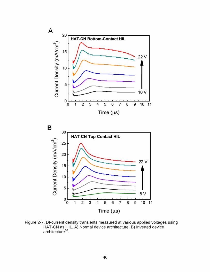
Figure 2-7. DI-current density transients measured at various applied voltages using HAT-CN as HIL. A) Normal device architecture. B) Inverted device architecture60.

47
Figure 2-8. Injection efficiency, η, extracted from DI-SCLC transient current measurements vs. electric field for normal and inverted NPB single-carrier devices with either MoO3 or HAT-CN as injection layer60.
Figure 2-9. Hole mobility (µDI) as a function of electric field (F1/2) for normal and inverted NPB hole-only devices with either MoO3 or HAT-CN injection layer. Field-dependent mobility based on time-of-flight (TOF) measurements is shown for comparison53,60.

48
Figure 2-10. Current density and injection efficiency plots for conventional NPB hole-only devices with either a neat MoO3 or MoO3-doped NPB HIL of varying doping concentration (1, 5, 10 mol%). A) J-E curves for the devices. B) Injection efficiency-electric field plot for the devices60.
49
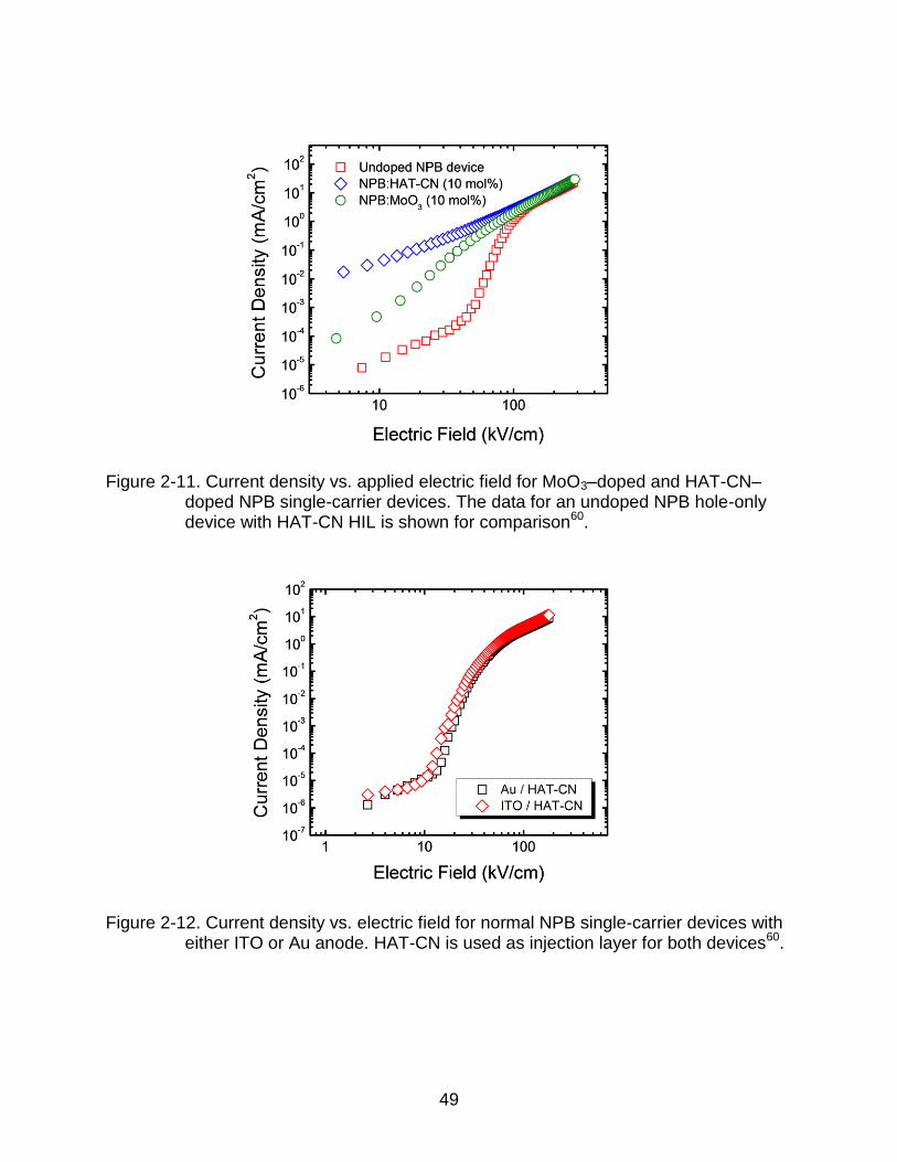
Figure 2-11. Current density vs. applied electric field for MoO3–doped and HAT-CN–doped NPB single-carrier devices. The data for an undoped NPB hole-only device with HAT-CN HIL is shown for comparison60.
Figure 2-12. Current density vs. electric field for normal NPB single-carrier devices with either ITO or Au anode. HAT-CN is used as injection layer for both devices60.
50
CHAPTER 3 INTRODUCTION TO ORGANIC PHOTOVOLTAIC CELLS
3.1 Overview and History
Due to the significant effort in the research and development of photovoltaic cells,
this renewable energy technology has become a promising candidate for meeting the
world's energy requirements. The state-of-the-art for this technology consist of
photovoltaic cells using inorganic materials such as silicon and compound
semiconductors. Photovoltaic cells and modules based on these materials have shown
high power conversion efficiencies, highlighting the potential of this technology to
achieve grid-parity. However, to achieve grid-parity, the total cost per watt would need
to be reduced for this technology to be competitive with non-renewable energy sources.
In an attempt to reduce the material and processing cost, thin-film inorganic photovoltaic
cells using materials such as amorphous/nanocrystalline Si, CdTe, and CuIn1-xGaxSe2
(CIGS) or Cu2ZnSn(S1-xSex)4 (CZTSSe) have been adopted61-63. Despite the potential
cost savings associated with these thin-film devices, their power conversion efficiency,
which is typically between 10−20%, is significantly lower than the state-of-the-art
technology64.
In addition to thin-film inorganic photovoltaic cells, devices based on organic
materials is a promising technology for low-cost energy harvesting. These organic
photovoltaic cells typically consist of either organic molecules of well-defined molecular
weight, structure and chemical composition, or conjugated polymers with high molecular
weight but a polydispersity index (PDI) greater than 1. Organic photovoltaic cells are
intrinsically flexibility, mechanical robust, and can be processed on inexpensive
substrates using high-throughput methods. For example, small molecule OPVs are

51
generally processed by high vacuum thermal evaporation and can be processed in high
throughput using this method65,66. Similarly, devices based on conjugated polymers and
novel oligomers can be fabricated by solution processing methods that are large-scale
roll-to-roll (R2R) processing compatible, such as slot-die coating, doctor blading, and
ink-jet printing67-70. Figure 3-1 illustrates various processing methods utilized in the
fabrication of large-area and laboratory-scale organic solar cells. Organic photovoltaic
cells also have an additional benefit associated with the design of organic small
molecules and conjugated polymers: the electronic and optical properties of these
organic materials can be modified by altering their chemistry. For example, one
approach for enhancing the performance of organic photovoltaic cell is to manipulate
the chemical structure of the electron donor. Modifications such as introducing electron
withdrawing groups, reducing the conjugated length, or enhancing the planarity of the
polymer can lower the bandgap, lower the HOMO level, or increase the polymer's
carrier mobility, respectively71,72. Such intelligent design of the conjugated polymer has
lead to enhanced Jsc and Voc in laboratory-scale organic photovoltaic cells.
Despite these advantages, the properties of the organic materials employed in
organic photovoltaic cells have introduced a number of issues that have impacted
device design. One of the key challenges with organic photovoltaic cells is to efficiently
dissociate tightly bound electron-hole pairs, called excitons, generated within the
organic seminconductor. There are two types of excitons formed in organic
semiconductors: Frenkel excitons and charge-transfer excitons (CTEs)73,74. Frenkel
excitons consist of electron-hole pairs with a binding distance less than a single
molecule, while charge-transfer excitons are characterized as electron-hole pairs that
52
are delocalized over adjacent molecules. The binding energy for these excitons are both
greater than 0.1 eV73,74. To separate these tightly-bound excitons, the first organic
photovoltaic cells utilized Schottky diodes to facilitate exciton dissociation. Although the
strong electric field near the metal electrode-organic interface dissociated excitons and
generated charge carriers, exciton quenching at this interface and limited exciton
dissociation throughout the photoactive layer limited the overall device performance75-77.
In 1986, a major breakthrough in organic photovoltaic cell performance was achieved by
Ching Tang with the demonstration of the donor-acceptor (D:A) bilayer heterojunction
photovoltaic78. A schematic diagram illustrating the D:A bilayer heterojunction structure
is show in Figure 3-2. In the bilayer heterojunction photovoltaic cell, excitons generated
within the organic materials dissociate at the heterojunction assuming that the energy
level offset between the donor and acceptor are large enough to provide a sufficient
driving force. For efficient device operation, the thickness of the donor and acceptor
layers must be less than the exciton diffusion length (LD)79. Although the shift to the
bilayer D:A heterojunction structure lead to enhanced photocurrent produced by the
device, exciton dissociation was still limited since the PV cells consisted of only one D:A
interface. In the 1990's, a further enhancement in exciton dissociation was
demonstrated in OPVs through the development of the D:A bulk heterojunction (BHJ)
photovoltaic cell79-81. In BHJ photovoltaic cells, the interpenetrating network created by
the D:A blend resulted in enhanced exciton dissociation since photogenerated excitons
now were within LD (see Figure 3-2). Significant enhancements in photocurrent were
observed for these photovoltaic cells as compared to bilayer heterojunction devices. In
more recent work, improvements to BHJ structure (optimizing the D:A blend

53
morphology, incorporating anode/cathode interlayers) and modification of the donor
conjugated polymer's energy levels have led to a world record power conversion
efficiency of 9.21% in single junction devices82.
3.2 Principles of Operation
To better appreciate the progress that has been made in organic photovoltaic cell
research, it is important to understand the operating principles of these devices. The
ability to generate power in an OPV cell is dependent on four processes that
sequentially occur with the photoactive layer. These processes are as follows: photon
absorption, exciton diffusion, charge transfer (exciton dissociation), and charge carrier
collection. The external quantum efficiency (EQE, ), or the ratio of the number of
charge carriers collected by the photovoltaic cell to the number of photons incident on
the device, is the product of the efficiencies associated with each of the four processes:
(3-1)
where is the photon absorption efficiency, is the exciton diffusion efficiency,
is the efficiency of charge transfer, and is the charge carrier collection efficiency.
This expression can also be written as:
(3-2)
where is the internal quantum efficiency. In the ideal case, a value
approaching unity can be achieved if both and are maximized. However, in the
state-of-the-art OPV cells, the processes influencing absorption efficiency and internal
quantum efficiency are opposing. Since organic semiconductors have a high absorption
coefficient ( ) of ~104 to 105 cm-1, the optical absorption length ( ) in these materials
is typically at least 100 nm83,84. As a result, increasing the photoactive layer thickness in

54
BHJ OPV cells above 100 nm enhances . However, charge carrier collection
becomes limited due to recombination losses in the thicker photoactive layer. Research
efforts have focused on enhancing device performance despite this tradeoff between
and . Chapter 4 will demonstrate an approach to enhance charge carrier collection
through the use of novel interlayers, while Chapter 5 will highlight this tradeoff problem
for high efficiency polymer photovoltaic cells with increased active layer thickness.
3.3 Photovoltaic Cell Characterization
The key parameters used to characterize organic photovoltaic cells under
operation will be discussed herein. In general, photovoltaic cells act as photodiodes
which operate when unbiased and show rectifying behavior. These devices differ from
typical photodiodes in that a wide spectral response over a broad solar wavelength
range is required85. The current-voltage (J-V) characteristics for a photovoltaic cell in the
dark and under illumination is shown in Figure 3-3. The J-V characteristics for the
effective photocurrent (Jph), which is the difference between the current under
illumination (JL) and the dark current (JD), is also shown. From the JL-V curve, the key
parameters used to characterize the device performance can be extracted. The short-
circuit current (Jsc), the photocurrent at zero bias, and the open-circuit voltage(Voc), the
voltage at which the JL = 0, is highlighted in the figure. The product of the Jsc and Voc is
the theoretical maximum power produced from the cell. The actual maximum power
output (Pm = Im × Vm) is typically less than this theoretical maximum. The determination
of Pm is illustrated by a small rectangle in Figure 3-3. The fill factor (FF) measures the
sharpness of the JL-V curve and is defined as the ratio between the actual and
theoretical maximum power outputs85,

55
(3-3)
The most important figure-of-merit is the power conversion efficiency ( ), which is the
ratio of the maximum power output to the incident power Pinc,
(3-3)
3.3.1 Current-Voltage Measurement
To experimentally determine , the J-V characteristics of the organic photovoltaic
cell were measured in the dark and under Air Mass 1.5 global (AM 1.5G) illumination.
The standard reporting conditions (SRC) for rating the performance of terrestrial
photovoltaic cells are as follows: 100 mW cm-2 (1 sun), AM 1.5G reference spectrum,
and 298 ºK cell temperature. To measure the current-voltage characteristics, a standard
test method for photovoltaic cells was utilized86. A xenon lamp with 1.5G air mass filter
was used to simulate the solar spectrum. The incident light from the solar simulator was
calibrated using a certified Si reference cell to ensure that Pinc = 100 mW cm-2. To
control the incident light intensity, neutral density filters were used so Pinc could be
varied from 10 to 100 mW cm-2. With the J-V characteristics measured, the key
parameters described in the previous section can be extracted.
3.3.2 Spectral Response Measurement
To experimentally determine , a spectral responsivity measurement was
performed on the organic photovoltaic cells studied in this work. A computer-controlled
spectral responsivity measurement system that met the ASTM E1021 testing standard
was used for this measurement87. The measurement system consisted of a 150 W
xenon arc lamp solar simulator with a 1.5G AM filter coupled with a monochromator as

56
the light source, producing monochomatic light with wavelengths from 400 nm to 1800
nm. The light beam from the monochromator is collimated and chopped using a
collimating lens and a optical chopper, respectively. The optical chopper creates an
alternating signal which allows the photocurrent produced by the test cell to be
differentiated from the background noise. By connecting the chopper to a lock-in
amplifier and using the chopper frequency (~400 Hz) as a reference , the photocurrent
signal can be isolated. The chopped monochromatic light then passes through a
condensing lens to either a calibrated Si photodetector for measuring the wavelength-
dependent incident light power or to the test cell. The beam spot size is less than both
the Si photodetector area and the test cell area for accuracy. A labVIEW program was
used to control the testing procedure and acquire the relevant data.
The spectral responsivity and, ultimately, the external quantum efficiency
spectrum can now be calculated. The spectral responsivity for the test cells, , is
calculated as follows:
(3-4)
where is the measured photocurrent density of the test cell, is the
incident light power measured with the Si photodetector, is the Si photodetector
current density, and is the responsivity of the reference detector. The external
quantum efficiency, also known as the incident photon-to-current efficiency (IPCE), can
now be calculated as
(3-5)

57
where h is Planck's constant, c is the speed of light, q is the electron charge, and is
the wavelength. Lastly, the short-circuit current density under AM 1.5G illumination at
100 mW cm-2 can be calculated from the external quantum efficiency spectrum as
(3-5)
where is the reference AM 1.5G power intensity. Ideally, the integrated Jsc
calculated from the EQE spectrum should match the value extracted from the J-V
characterization for the test cells. This is only possible if the calibrations for both the J-V
measurement setup and the spectral responsivity measurement setup are done
correctly.
3.4 Progress in Organic Photovoltaic Cell Performance
Since the first demonstration of organic photovoltaic cells utilizing the BHJ
structure, research efforts have focused on enhancing the power conversion efficiency
of these devices. Improving the properties of the conjugated polymers and organic small
molecules used as the donor in the D:A blend through intelligent chemical design has
been largely responsible for the high efficiencies reported in the literature88-90. These
materials are typically blended with C60 fullerene or its derivatives to facilitate exciton
dissociation within the photoactive layer. C60 derivatives, such as [6,6]-phenyl-C61-
butyric acid methyl ester (PCBM), have become the standard n-type materials used in
OPV cells due to their high electron mobility and strong electronegativity91. This section
will discuss the chemical design and important material properties of the novel
conjugate polymers employed in Chapters 4 and 5 of this dissertation, as well as similar
polymers reported in the literature. Furthermore, the power conversion efficiencies
reported for polymer BHJ OPV cells incorporating these polymers will be highlighted.
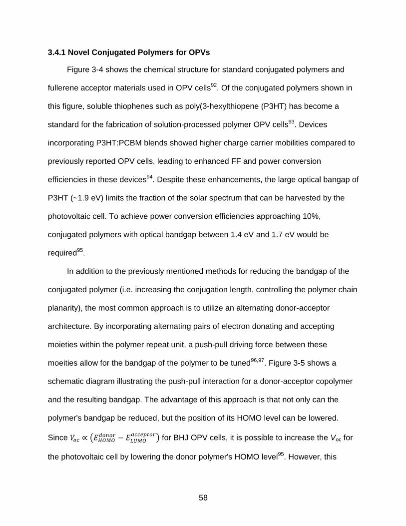
58
3.4.1 Novel Conjugated Polymers for OPVs
Figure 3-4 shows the chemical structure for standard conjugated polymers and
fullerene acceptor materials used in OPV cells92. Of the conjugated polymers shown in
this figure, soluble thiophenes such as poly(3-hexylthiopene (P3HT) has become a
standard for the fabrication of solution-processed polymer OPV cells93. Devices
incorporating P3HT:PCBM blends showed higher charge carrier mobilities compared to
previously reported OPV cells, leading to enhanced FF and power conversion
efficiencies in these devices94. Despite these enhancements, the large optical bangap of
P3HT (~1.9 eV) limits the fraction of the solar spectrum that can be harvested by the
photovoltaic cell. To achieve power conversion efficiencies approaching 10%,
conjugated polymers with optical bandgap between 1.4 eV and 1.7 eV would be
required95.
In addition to the previously mentioned methods for reducing the bandgap of the
conjugated polymer (i.e. increasing the conjugation length, controlling the polymer chain
planarity), the most common approach is to utilize an alternating donor-acceptor
architecture. By incorporating alternating pairs of electron donating and accepting
moieties within the polymer repeat unit, a push-pull driving force between these
moeities allow for the bandgap of the polymer to be tuned96,97. Figure 3-5 shows a
schematic diagram illustrating the push-pull interaction for a donor-acceptor copolymer
and the resulting bandgap. The advantage of this approach is that not only can the
polymer's bandgap be reduced, but the position of its HOMO level can be lowered.
Since
for BHJ OPV cells, it is possible to increase the Voc for
the photovoltaic cell by lowering the donor polymer's HOMO level95. However, this

59
approach is not without its disadvantages. As shown in Figure 3-5, the HOMO level for
the copolymer is centralized around the donor unit while the LUMO level resides on the
acceptor unit. For efficient hole transport along the copolymer's HOMO level, the donor
unit must be in close proximity to other donor units. The same is true for electron
transport along the copolymer's LUMO level, which is centralized around the acceptor
unit. Therefore, interchain packing becomes critically important for sufficient carrier
transport in donor-acceptor copolymers.
Figure 3-6 displays the chemical structure of representative donor-acceptor
copolymers used in state-of-the-art polymer solar cells. Initial progress in the
development of these novel polymers was made by incorporating the acceptor unit
benzothiadiazole (BTD) into the copolymer. Examples include the copolymers poly[2,6-
(4,4-bis-(2-ethylhexyl)-4H-cyclopenta[2,1-b;3,4-b']dithiophene)-alt-4,7-(2,1,3-
benzothiadiazole)] (PCPDTBT) and poly[N-9"-hepta-decanyl-2,7-carbazole-alt-5,5-(4',7'-
di-2-thienyl-2',1',3'-benzothiadiazole)] (PCDTBT), both of which have shown power
conversion efficiencies from 5.5% to 6.1% when incorporated in optimized polymer BHJ
solar cells90,98. A further enhancement in device performance was observed for donor-
acceptor polymers composed of either benzodithiophene (BDT) or thienopyrrolodione
(TPD) as the acceptor unit99,100. For example, Reynolds and coworkers demonstrated
high efficiency polymer solar cells incorporating a dithienosilole-fused (DTS) or
dithienogermole-fused (DTG) donor-acceptor copolymer with TPD as the acceptor
unit101. Replacing the carbon bridging atom in the donor unit with Si or Ge improved
molecular chain packing in the BHJ film, leading to increased FF and power conversion
efficiencies over 7% for the solar cell. Such manipulations to the chemical structure of
60
the conjugated polymer's has been vital to the continued improved of polymer solar cell
performance.
3.4.2 Inverted Device Geometry
In addition to developing novel conjugated polymers for improved light harvesting
and increased Voc, researchers have also focused on the inverted device architecture
for improved polymer solar cell stability and large-scale roll-to-roll (R2R) processing
compatibility. A schematic of the conventional and inverted geometries employed for
polymer solar cell fabrication is shown in Figure 3-7. In the inverted architecture, the
device stability is improved since unfavorable materials such as acidic PEDOT:PSS and
low work function metals are replaced by more favorable materials. Novel anode and
cathode interlayers, which modify the work function of the electrodes and thus form
Ohmic contacts for improved carrier extraction, have enabled high efficiency polymer
solar cells with an inverted geometry to be realized. These interlayers also serve as
selective contacts for electron or hole transport while effectively blocking the opposing
charge carrier. Presently, novel interlayers for inverted polymer solar cells include n-
type materials like TiOx, ZnO, and water/alcohol soluble polyfluorenes, while transition
metal oxides such as MoO3 and V2O5 have been successfully used as anode interlayers
for improved carrier extraction102-104. Using this approach, world-record certified power
conversion efficiencies of over 9% has been demonstrated82.
In Chapter 4, high efficiency inverted polymer solar cells based on
polydithienogermole-thienopyrrolodione (PDTG-TPD) will be discussed. The focus of
that discussion will be on the materials characterization and electronic properties of a
novel ZnO composite electron transporting layer employed in the device. The impact of
this result on demonstrating the commercial viability of OPV cells with be highlighted. In

61
Chapter 5, the active layer thickness dependence of the power conversion efficiency will
be investigated for inverted solar cells with novel low-bandgap polymers. Furthermore,
the consequence of space-charge formation on carrier extraction will be discussed.

62
Figure 3-1. Schematic illustrations for various solution processing methods used in the fabrication of large-scale and laboratory-scale polymer photovoltaic cells. A) Screen printing. B) Spin coating. C) knife-over-edge, slot-die, gravure, and meniscus coating105.
Figure 3-2. Schematic diagram illustrating an organic donor-acceptor heterjunction, as well as the bilayer and bulk heterojunction concepts. A) The D:A heterojunction. B) The bilayer heterojunction device structure. C) The bulk heterojunction device structure. Taken from: M. Riede. I-CAMP 2012 Lecture, Topic: "Vacuum Processing and the p-i-n Concept for OPV." Boulder, CO, July 7, 2012.
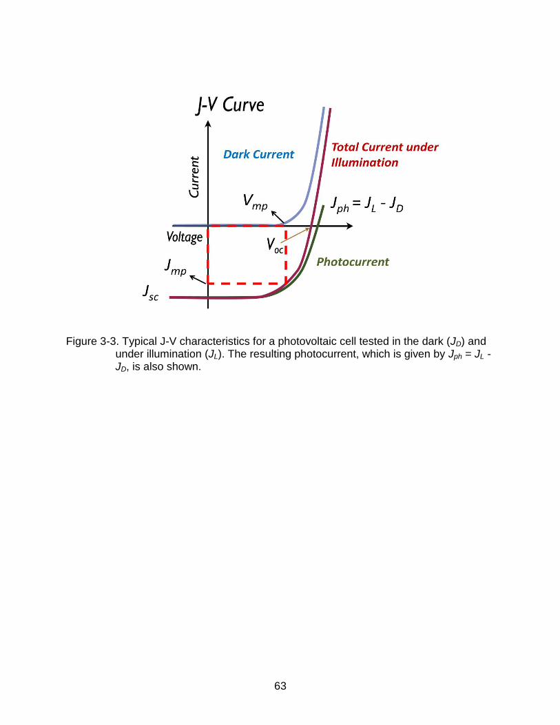
63
Figure 3-3. Typical J-V characteristics for a photovoltaic cell tested in the dark (JD) and under illumination (JL). The resulting photocurrent, which is given by Jph = JL - JD, is also shown.
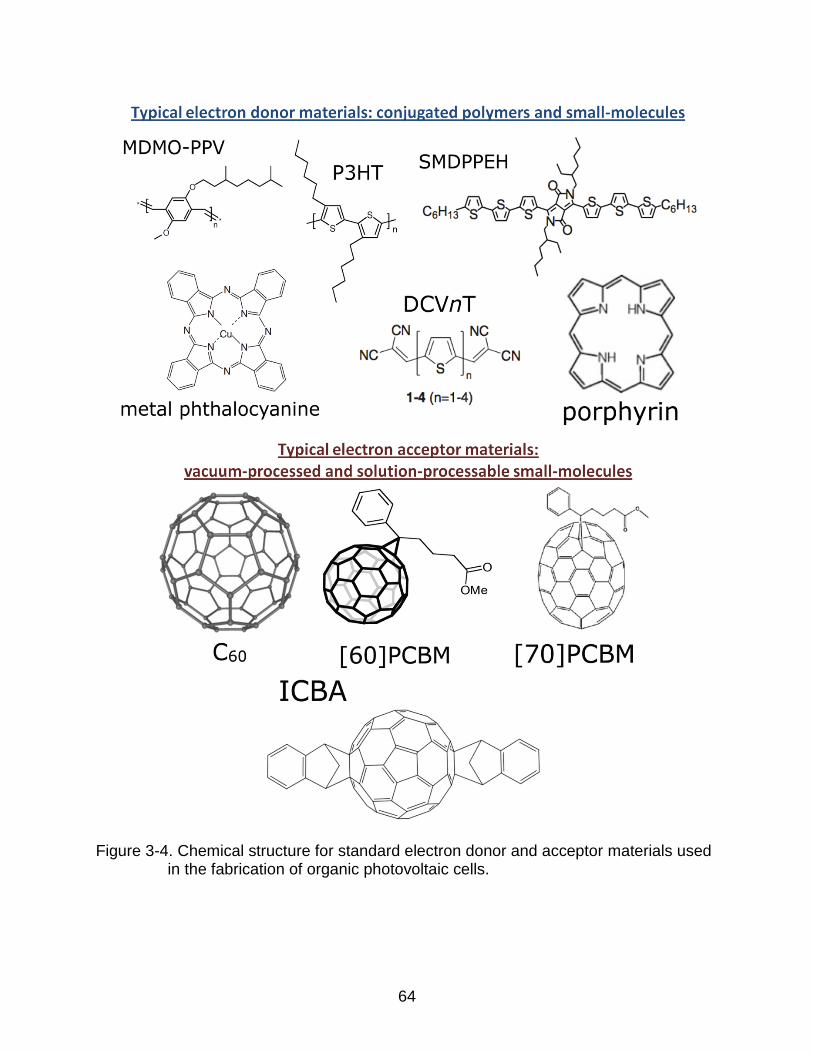
64
Figure 3-4. Chemical structure for standard electron donor and acceptor materials used in the fabrication of organic photovoltaic cells.
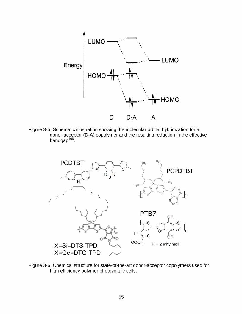
65
Figure 3-5. Schematic illustration showing the molecular orbital hybridization for a donor-acceptor (D-A) copolymer and the resulting reduction in the effective bandgap106.
Figure 3-6. Chemical structure for state-of-the-art donor-acceptor copolymers used for high efficiency polymer photovoltaic cells.

66
Figure 3-7. Normal vs. inverted device architectures for organic photovoltaic cells107.
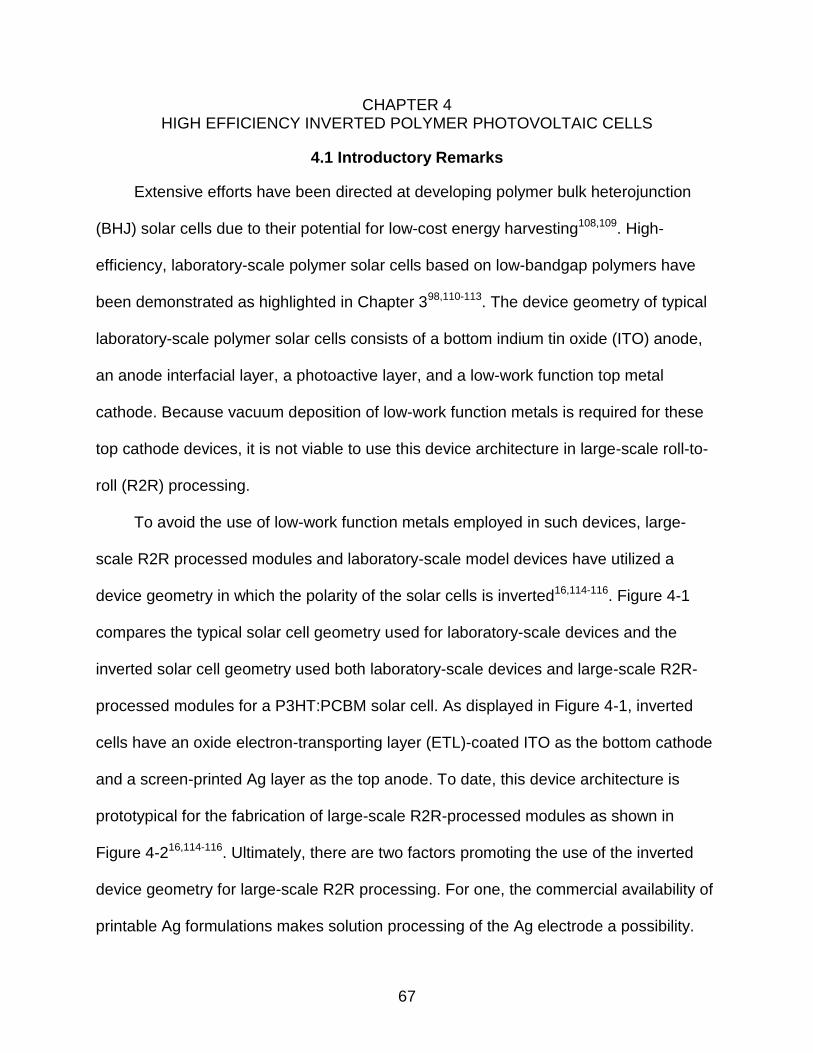
67
CHAPTER 4 HIGH EFFICIENCY INVERTED POLYMER PHOTOVOLTAIC CELLS
4.1 Introductory Remarks
Extensive efforts have been directed at developing polymer bulk heterojunction
(BHJ) solar cells due to their potential for low-cost energy harvesting108,109. High-
efficiency, laboratory-scale polymer solar cells based on low-bandgap polymers have
been demonstrated as highlighted in Chapter 398,110-113. The device geometry of typical
laboratory-scale polymer solar cells consists of a bottom indium tin oxide (ITO) anode,
an anode interfacial layer, a photoactive layer, and a low-work function top metal
cathode. Because vacuum deposition of low-work function metals is required for these
top cathode devices, it is not viable to use this device architecture in large-scale roll-to-
roll (R2R) processing.
To avoid the use of low-work function metals employed in such devices, large-
scale R2R processed modules and laboratory-scale model devices have utilized a
device geometry in which the polarity of the solar cells is inverted16,114-116. Figure 4-1
compares the typical solar cell geometry used for laboratory-scale devices and the
inverted solar cell geometry used both laboratory-scale devices and large-scale R2R-
processed modules for a P3HT:PCBM solar cell. As displayed in Figure 4-1, inverted
cells have an oxide electron-transporting layer (ETL)-coated ITO as the bottom cathode
and a screen-printed Ag layer as the top anode. To date, this device architecture is
prototypical for the fabrication of large-scale R2R-processed modules as shown in
Figure 4-216,114-116. Ultimately, there are two factors promoting the use of the inverted
device geometry for large-scale R2R processing. For one, the commercial availability of
printable Ag formulations makes solution processing of the Ag electrode a possibility.
68
Second, the development of solution-processed transition metal-oxides such as TiOx
and ZnO has lead to their use in large-scale solar cell manufacturing as ETLs to reduce
the ITO work function117,118. In particular, ZnO colloidal nanoparticles are used for the
ETL because of their low work function, high electron mobility and optical transparency,
as well as their ease of synthesis119,120. However, the major challenges in using ZnO
nanoparticle films as ETLs are the presence of defects with adsorbed oxygen and poor
spatial distribution of the nanoparticles over a large area121-125. For example, the poor
spatial distribution observed in ZnO nanoparticle films is attributed to the formation of
aggregates, which is highlighted in the AFM image shown in Figure 4-3. This AFM
image of a knife-over-edge-coated ZnO nanoparticle film shows distinct particles with
height ~60 nm and diameter of ~300–500 nm, indicating that severe aggregation of the
ZnO nanoparticles is typical for large-scale processed films115. Accordingly, there is a
need to develop low-defect and uniform ZnO films so as to realize high-efficiency
inverted polymer solar cells.
Here, enhanced charge collection was demonstrated in inverted polymer BHJ
solar cells using a ZnO-poly(vinyl pyrrolidone) (PVP) composite sol-gel film as the ETL,
leading to devices that operate with laboratory-measured PCEs in excess of 8% and
certified efficiencies of 7.4% under AM 1.5G illumination at 100mW cm-2. The composite
film, termed ‘ZnO-PVP nanocomposite’ for clarity, consists of ZnO nanoclusters whose
growth is mediated by a PVP polymeric matrix126. ZnO-PVP nanocomposite films have
been previously studied for chemical/bio-sensing applications and have the following
advantages over conventional ZnO sol-gel films127-130. First, the ZnO nanocluster size
and its concentration can be tuned by controlling the Zn2+/PVP ratio127,128. Second, the

69
distribution of ZnO nanoclusters in the PVP polymer is uniform compared to the
aggregation observed in ZnO sol-gel films without PVP127,128. We hypothesized that
inverted solar cells using this composite would demonstrate enhanced device
performance. Furthermore, because the sol-gel processing for the ZnO-PVP
nanocomposite is performed in air, this approach to depositing the ZnO ETLs is
compatible with large-scale R2R processes.
The synthesis and BHJ solar cell performance of the polymer used in this study, a
dithienogermole (DTG)-containing alternating conjugated donor-acceptor polymer with
N-octylthienopyrrolodione (TPD) was used as the acceptor has been previously
reported101. Inverted polydithienogermole-thienopyrrolodione (PDTG-TPD):[6,6]-phenyl-
C71-butyric acid methyl ester (PC71BM) solar cells demonstrated a higher short-circuit
current density (Jsc) and fill factor (FF) than devices with an analogous
polydithienosilole-containing polymer (PDTS-TPD), leading to inverted polymer solar
cells with PCEs of 7.3%131. To determine whether our ZnO-PVP nanocomposite films
would enhance charge collection for inverted solar cells, inverted PDTG-TPD:PC71BM
BHJ solar cells was fabricated using the nanocomposite as an ETL. The following
inverted device geometry was used for our study: ITO/ZnO-PVP nanocomposite/PDTG-
TPD:PC71BM/anode interfacial layer/Ag. For the anode interfacial layer, molybdenum
trioxide (MoO3) was used, which has a better charge extraction efficiency than more
commonly used poly(ethylenedioxythiophene) doped with poly(styrene-sulfonate)
(PEDOT:PSS)101,132-135. While both MoO3 and Ag are thermally evaporated in our
devices, these electrode materials are compatible with R2R processing because MoO3

70
can be coated from a nanoparticles suspension136 and Ag paste can be screen
printed16,114-116.
4.2 Experimental Details
4.2.1 Device Fabrication
The detailed synthesis, polymer characterization and device fabrication and testing
for PDTG-TPD:PC71BM has been reported elsewhere110. PC71BM used for solar cell
fabrication was purchased from Solenne. Polymers and PC71BM were dissolved in
chlorobenzene with 1:1.5 (8 mg mL-1:12 mg mL-1) weight ratio and 5% volume ratio of
1,8-diiodooctane (DIO) was added as a processing additive prior to use. The ZnO-PVP
nanocomposite was prepared from a precursor, in which zinc acetate dihydrate
(Zn(CH3COO)2 · 2H2O, Aldrich, 99.9%, 11 mg ml-1) and polyvinylpyrollidone (PVP, 2.5
mg ml-1) were dissolved in ethanol. Ethanolamine was added to the precursor as a
stabilizer in equal molar concentration to zinc acetate dihydrate. The ZnO-PVP
precursor was spin-coated on indium tin oxide (ITO)-coated glass substrates, which
were first cleaned with detergent, ultrasonicated in DI water, acetone, and isopropyl
alcohol, and subsequently dried via N2. The films were annealed at 200 oC for 40
minutes in air. After annealing and slow-cooling to room temperature, the ZnO-PVP
composite films were UV-ozone treated using a UV-ozone cleaner. The film thicknesses
for the ZnO-PVP composite film before and after UV-ozone treatment were 36 nm and
33 nm, respectively. The polymer-fullerene solutions were then spin-coated and the
resulting film with thickness of 105 nm was annealed at 80 oC for 30 minutes. Finally,
thin films of MoO3 (10 nm) and Ag (100 nm) were deposited through shadow masks via
thermal evaporation. The active area of the device was 4.6 mm2.

71
4.2.2 Device Characterization
For PV measurements, a light mask with an area of 3.04 mm2 was used to define
the active area of the device. Device characterization was carried out in air after
encapsulation using an Air Mass 1.5 Global (A.M. 1.5G) solar simulator with irradiation
intensity of 100 mW cm-2. The beam spot used in EQE measurement was smaller than
the device area to ensure accuracy of the measurement.
4.3 Results and Discussions
4.3.1 ZnO-PVP Nanocomposite Film Characterization
Surface Morphology: The enhanced device performance with UV-ozone treated
ZnO-PVP nanocomposite films is believed to be attributable to the modified surface
composition promoting charge collection. The nanoscale surface morphologies of the
as-prepared and UV-ozone treated ZnO-PVP nanocomposite films were investigated by
atomic force microscopy (AFM). Fig. 4-4a and b shows the three-dimensional surface
topography images for the nanocomposite film before and after UV-ozone treatment.
The ZnO-PVP nanocomposite film shows an increase in r.m.s. roughness from 7.07 nm
to 9.18 nm following UV-ozone treatment, suggesting that PVP is removed with this
treatment, leaving the ZnO nanoclusters exposed at the surface. This removal of the
PVP is more clearly shown in the AFM phase images in Fig. 4-4c and d. For the
nanocomposite film without UV-ozone treatment, no nanoclusters can be observed,
indicating that the surface is covered by a thin layer of PVP. However, the phase image
for the UV-ozone treated ZnO-PVP nanocomposite film shows that the PVP domain
size has been reduced to 50-100 nm and that the ZnO nanoclusters are now exposed
on the surface. The PVP-rich and ZnO nanocluster-rich surfaces of the nanocomposite

72
films before and after UV-ozone treatment, respectively, are shown schematically in Fig.
4-4e,f.
To determine whether the removal of PVP from the nanocomposite film surface
altered the film thickness, step-height measurements were taken for the films before
and after UV-ozone treatment. The average thickness of the nanocomposite film shows
negligible change after 10 min UV ozone treatment, which provides further evidence
that PVP was removed only at the surface of the ZnO-PVP nanocomposite film upon
UV-ozone treatment. Furthermore, to illustrate the surface morphology of the ZnO-PVP
nanocomposite films before and after UV-ozone treatment, 5-µm-scale phase images
are shown in Fig. 4-5. These images show that the removal of PVP by UV-ozone
treatment significantly alters the surface morphology of the nanocomposite film. This
change in surface morphology from being PVP-rich before UV-ozone treatment to ZnO-
rich after treatment supports our idea that the removal of PVP from the nanocomposite
film by UV-ozone treatment leads to improved charge collection in our inverted polymer
solar cells due to better electronic coupling between the ZnO nanoclusters within the
nanocomposite film and PC71BM in the active layer.
Chemical Composition: To further confirm that the compositional changes
determined from the AFM data were due to the removal of PVP, X-ray photoemission
spectroscopy (XPS) was performed on the ZnO-PVP nanocomposite films. Considering
the period of UV-ozone treatment required to optimize the device performance, it is
believed that some changes in the chemical composition of ZnO might be plausible. The
core level XPS spectra for the C 1s, O 1s, and Zn 2p were measured for the as-
prepared and 10 min UV-ozone treated ZnO-PVP nanocomposite films. The binding

73
energies were calibrated by taking the C 1s peak (284.6 eV) as a reference. The O 1s
XPS spectra for as-prepared and UV-ozone treated ZnO-PVP nanocomposite films are
shown in Fig. 4-6a. UV-ozone treatment increased the relative magnitude of the peak at
531.4 eV (corresponding to the oxygen atoms bonded to the zinc in the ZnO
matrix127,128,137) by ~37%. Thus the number of Zn-O bonds in the wurtzite structure of
ZnO at the surface of the film is increased. UV-ozone treatment also increased the
relative magnitude of the peak at ~ 530.0 eV, which corresponds to O-2 ions present in
the porous ZnO clusters, but not chemically bonded to zinc in the ZnO wurtzite
structure. Fig. 4-6b shows the Zn 2p3/2 XPS spectra for the as-prepared and UV-ozone
treated ZnO-PVP nanocomposite films. The intensity of the peak at 1021.6 eV, which
corresponds to the Zn-O bonds127,128,137,138, increases after UV-ozone treatment. These
results are in agreement with the result from the O 1s XPS spectra. Based on the O 1s
and Zn 2p XPS spectra, we conclude that the chemical composition of the ZnO
nanoclusters on the surface of the nanocomposite film has become oxygen-rich after
UV-ozone treatment.
The atomic concentrations of carbon, oxygen, and zinc in the as-prepared and 10
min UV-ozone treated ZnO-PVP nanocomposite films based on the C 1s, O 1s, and Zn
2p XPS spectra are summarized in Fig. 4-6c. The atomic concentration of carbon from
the PVP in the nanocomposite is significantly reduced by UV-ozone treatment (from
38.2% to 15.7%). Conversely, the atomic concentrations of oxygen and zinc present in
the nanocomposite film both increase from 28.5% and 33.3% for the untreated film to
31.6% and 52.6%, respectively, for the treated film. The relatively smaller increase in
oxygen atomic concentration compared to zinc is due to the competition between the
74
increases in oxygen content coming from UV-Ozone treatment and the decrease in
oxygen content coming from the removal of PVP. These results strongly support our
assertion that UV-ozone treatment removes PVP from the surface of the ZnO-PVP
nanocomposite film.
Optical Transparency: Finally, the effect of UV-ozone treatment on optical
transmission for the as-prepared and treated ZnO-PVP nanocomposite films was
studied. UV-vis-NIR transmission spectra for these films are shown in Supplementary
Fig. 4-7. Following UV-ozone treatment, a 6% to 10% increase in transmission across
the entire visible spectrum was observed in the nanocomposite film. This increase in
optical transmission was attributed to the changes in the effective index of refraction of
the nanocomposite film upon UV-ozone treatment. It should be noted that the increase
in optical transparency is less than the enhancement observed in Jsc for inverted solar
cells with UV-ozone treated ZnO-PVP nanocomposite films. Therefore, although the
increase in optical transparency contributes to the enhancement in Jsc, the improved
charge collection due to enhanced electronic coupling between ZnO nanoclusters in the
nanocomposite film and PC71BM in the active layer is primarily responsible for this
enhancement.
4.3.2 Inverted Polymer Photovoltaic Cell with ZnO-PVP Nanocomposite ETL
The photo J-V characteristics for inverted PDTG-TPD:PC71BM solar cells were
measured under AM 1.5G solar illumination at 100 mW cm-2. The photovoltaic (PV)
performance results for the inverted cells with ZnO-PVP nanocomposites are shown in
Fig. 4-8. On initial light exposure the inverted solar cells had a low FF of 25.5% and Jsc
of 10.9 mA cm-2. With continuous illumination, device performance was enhanced
significantly over time139. After ~10 min of light soaking, an enhanced FF of 63.7% and

75
Jsc of 12.9 mA cm-2 were obtained, resulting in an average PCE of 7.0%. Previously, we
reported inverted PDTG-TPD-based polymer solar cells with FF of ~68% using colloidal
ZnO NPs as ETL101. We suspected that by using ZnO-PVP composite as the ETL, the
ZnO-PVP surface would be compositionally rich in PVP, creating a contact barrier
between the ZnO nanoclusters and PC71BM lead to the lower FF of our present devices.
To ensure a good contact between the ZnO nanoclusters and PC71BM, we
performed UV-ozone treatment on the ZnO-PVP nanocomposite films to remove PVP
from the surface. Previous work has shown that UV-ozone treatment can remove PVP
on colloidal nanoparticle film surfaces140. The removal of PVP did not alter the size,
shape, or distribution of the nanoclusters in the films140,141. Based on these findings, we
believed that the UV-ozone treatment would improve electronic coupling between
photo-active layer and ZnO nanoclusters.
The photo J-V characteristics for the inverted PDTG-TPD:PC71BM solar cells with
UV-ozone treated ZnO-PVP nanocomposites are shown in Fig. 4-9a. All devices were
tested under initial light exposure, and no additional light soaking was applied to the
devices. The ZnO-PVP nanocomposite films were UV-ozone treated for 5, 10, 20, and
30 min, leading to significant enhancements in Jsc and FF for the inverted PDTG-
TPD:PC71BM solar cells compared to cells with as-prepared nanocomposite films.
Table 4-1 summarizes the device performance for inverted solar cells with treated ZnO-
PVP nanocomposite films. UV-ozone treating the ZnO-PVP nanocomposite films for 10
min led to an optimal device with enhancements in both Jsc and FF compared to the
light-soaked devices without UV-ozone treatment, resulting in an average PCE of 8.1%.
This average PCE of 8.1 ± 0.4% is based on measurement from 102 fabricated solar

76
cells. Our best device had a Jsc of 14.4 mA cm-2, Voc of 0.86 V, FF of 68.8% and PCE of
8.5%. For devices with ZnO-PVP nanocomposite films that had been UV-ozone treated
for less than or more than 10 min, a reduction in FF was observed. For the shorter
treatment, we attribute this reduction in FF to incomplete removal of the PVP from the
surface of the composite film. For the longer treatment, excess oxygen is present on the
ZnO film surface, which reduces the electron extraction efficiency. Based on these
findings, we conclude that removal of extra PVP from the ZnO-PVP nanocomposite film
surface by UV-ozone treatment greatly enhances the charge collection efficiency of
these devices.
To confirm the accuracy of the photo J-V measurements, the external quantum
efficiency (EQE) spectra for the solar cells with as-prepared and 10 min UV-ozone
treated ZnO-PVP nanocomposite films were measured; these are compared in Fig. 4-
9b. An enhanced efficiency is observed throughout the full spectral range from 350 –
700 nm for cells with the UV-ozone treated ZnO-PVP nanocomposite films when
compared to cells without UV-ozone treatment. The maximum EQE for the optimized
inverted PDTG-TPD:PC71BM solar cell with UV-ozone treated nanocomposite films was
73.6%. The Jsc value was then calculated by integrating the EQE data with the AM 1.5G
spectrum. The calculated Jsc value of 14.5 mA cm-2 is in good agreement with the
directly measured Jsc value.
To study the difference in light soaking behavior for inverted PDTG-PC71BM solar
cells with either as-prepared or UV-ozone treated ZnO-PVP nanocomposite ETL, dark
J-V measurements were taken on the inverted devices before and after AM 1.5G solar
illumination. Fig. 4-10 shows the results for inverted devices measured with either no

77
light soaking or with light soaking using filters to block incident light below 600 nm or
350 nm wavelength. The devices were encapsulated and stored in the dark prior to
measurements. The dark J-V curves for the device before light soaking and after light
soaking using the 600 nm filter are identical, showing low current density values for the
inverted devices. Therefore, long wavelength light soaking has no effect on device
performance. However, when the inverted device is light soaked using the 350 nm long-
pass filters, a significant enhancement in dark current density is observed. The
enhanced dark current density matches the values observed for typical dark J-V
measurements of these devices under forward bias. Therefore, the inverted solar cells
with UV-ozone treated ZnO-PVP shows immediate enhancement in conductivity upon
illumination of short wavelength light. The fact that we see optimized performance
during the initial J-V scan for the UV-ozone treated device indicates that the soaking
time required is significantly less than that required for the untreated devices.
Encapsulated devices with UV-ozone treated ZnO-PVP nanocomposite films were
then sent to NEWPORT Corporation for certification. The photo J-V characteristics and
the corresponding solar cell parameters are shown in Fig. 4-11. A PCE of 7.4 +/- 0.2%
was certified for the devices. Although this certified efficiency is 9% less than that
measured in our laboratory because of a reduction in Jsc and FF in the certified device,
we attribute the reduction in PCE in the certified cells to degradation because of a non-
optimized encapsulation process. The devices were retested in our laboratory after
certification and we obtained an efficiency (7.2%) comparable to the certified results.
We sought to further investigate the effect of UV-ozone treatment on ZnO-PVP
composite films and the corresponding photovoltaic device stability. As shown in Fig. 4-

78
12, after light soaking, the performance of the device with untreated ZnO-PVP
nanocomposite ETL reduced significantly over time, showing that the enhancement in
Jsc and FF due to light soaking was only temporary139. In contrast, the device
performance observed for solar cells with UV-ozone treated ZnO-PVP nanocomposite
ETLs had much better stability. In fact, we observed no measureable changes in Jsc,
FF, or PCE over a period of one month provided that the encapsulated devices were
stored in a nitrogen glove box. Thus, UV-ozone treatment of the ZnO-PVP
nanocomposite films provides enhanced stability in the inverted solar cells.
4.3 Concluding Remarks
To conclude, improved charge collection efficiency has been demonstrated in
inverted PDTG-TPD BHJ solar cells using a UV-ozone treated ZnO-PVP
nanocomposite film as the ETL to obtain organic polymer solar cells with PCEs in
excess of 8% under A.M.1.5G illumination at 100 mW cm-2. The use of PVP as an
organic capping molecule and polymeric matrix for ZnO produced electron-transporting
nanocomposite films, which had excellent film-forming characteristics. We found that
UV-ozone treatment was required to remove PVP from the surface of the film, and
consequently exposed the ZnO nanoclusters to the film surface. Using our UV-ozone
treated ZnO-PVP nanocomposite ETL, inverted PDTG-TPD solar cells with laboratory-
measured PCE higher than 8% have been realized due to improved charge collection
by the nanocomposite film.

79
Table 4-1. Average solar cell performance for inverted PDTG-TPD:PC71BM devices with 5, 10, 20, or 30-minute UV-ozone treated ZnO-PVP composite ETLs under initial AM 1.5G solar illumination142.
UV-ozone treatment time
Jsc (mA cm-2)
Voc (V) FF (%) Average PCE
(%) Best
PCE (%)
5 min 13.9±0.1 0.85±0.005 56.0±3.8 6.6±0.5 7.1 10 min 14.0±0.4 0.86±0.003 67.3±1.5 8.1±0.4 8.5 20 min 14.1±0.2 0.86±0.003 64.8±0.8 7.8±0.2 8.0 30 min 14.0±0.1 0.86±0.003 61.9±1.6 7.5±0.3 7.6
Figure 4-1. The normal and inverted device geometries for P3HT:PCBM solar cells. A) The normal device geometry. B) The inverted device geometry116.
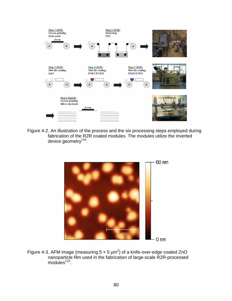
80
Figure 4-2. An illustration of the process and the six processing steps employed during fabrication of the R2R coated modules. The modules utilize the inverted device geometry116.
Figure 4-3. AFM image (measuring 5 × 5 µm2) of a knife-over-edge coated ZnO nanoparticle film used in the fabrication of large-scale R2R-processed modules115.
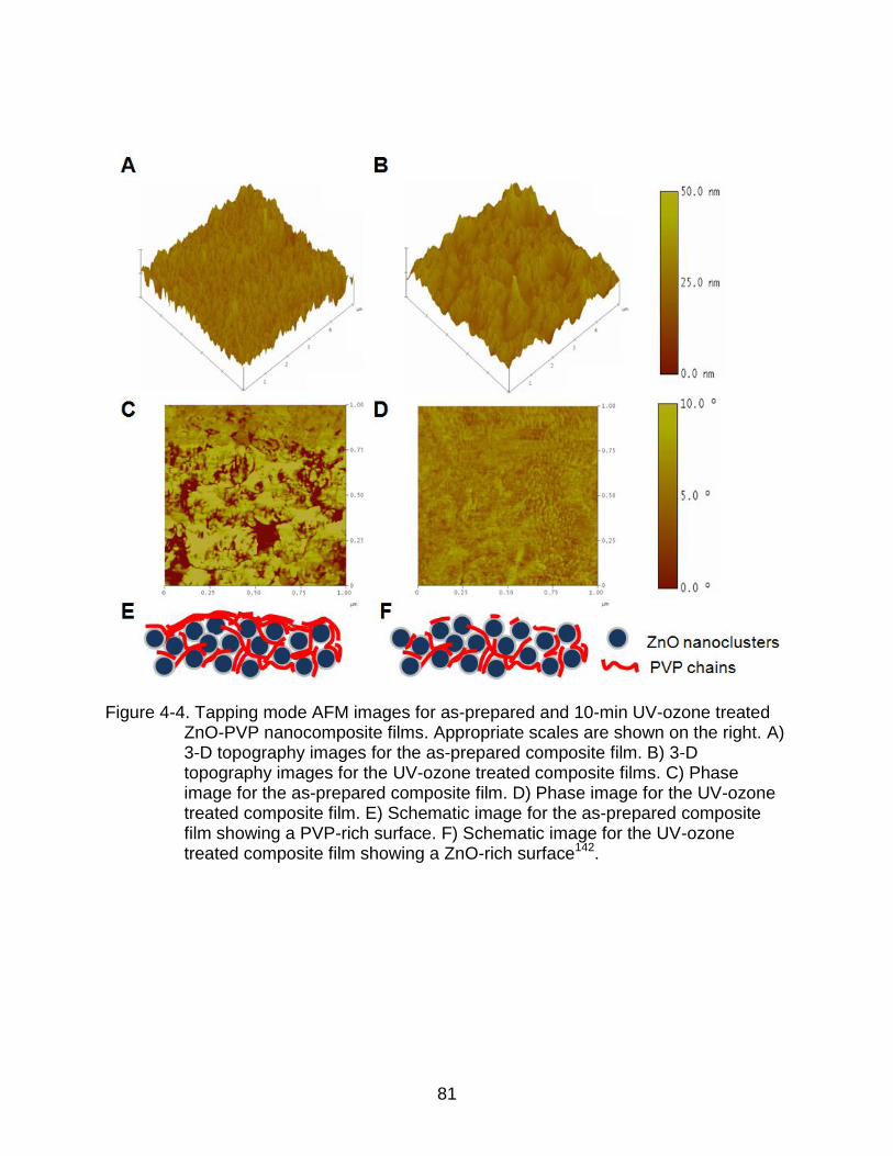
81
Figure 4-4. Tapping mode AFM images for as-prepared and 10-min UV-ozone treated ZnO-PVP nanocomposite films. Appropriate scales are shown on the right. A) 3-D topography images for the as-prepared composite film. B) 3-D topography images for the UV-ozone treated composite films. C) Phase image for the as-prepared composite film. D) Phase image for the UV-ozone treated composite film. E) Schematic image for the as-prepared composite film showing a PVP-rich surface. F) Schematic image for the UV-ozone treated composite film showing a ZnO-rich surface142.

82
Figure 4-5. Tapping-mode AFM phase images for ZnO-PVP nanocomposite films before and after UV-ozone treatment (5 µm scale size). A) As-prepared composite films. B) 10-minute UV-ozone treated composite film142.
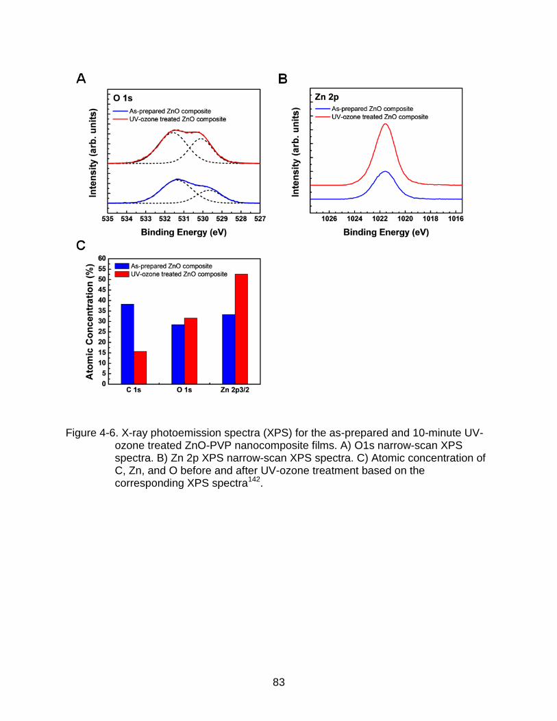
83
Figure 4-6. X-ray photoemission spectra (XPS) for the as-prepared and 10-minute UV-ozone treated ZnO-PVP nanocomposite films. A) O1s narrow-scan XPS spectra. B) Zn 2p XPS narrow-scan XPS spectra. C) Atomic concentration of C, Zn, and O before and after UV-ozone treatment based on the corresponding XPS spectra142.
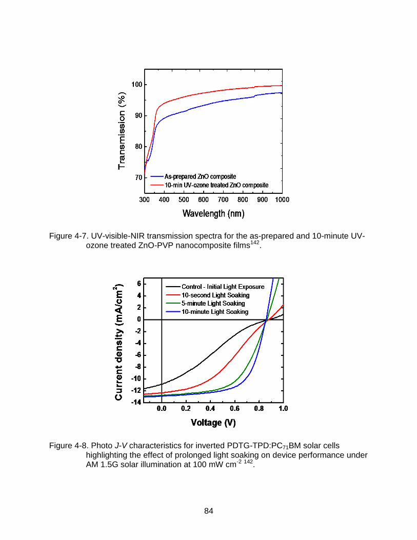
84
Figure 4-7. UV-visible-NIR transmission spectra for the as-prepared and 10-minute UV-ozone treated ZnO-PVP nanocomposite films142.
Figure 4-8. Photo J-V characteristics for inverted PDTG-TPD:PC71BM solar cells highlighting the effect of prolonged light soaking on device performance under AM 1.5G solar illumination at 100 mW cm-2 142.
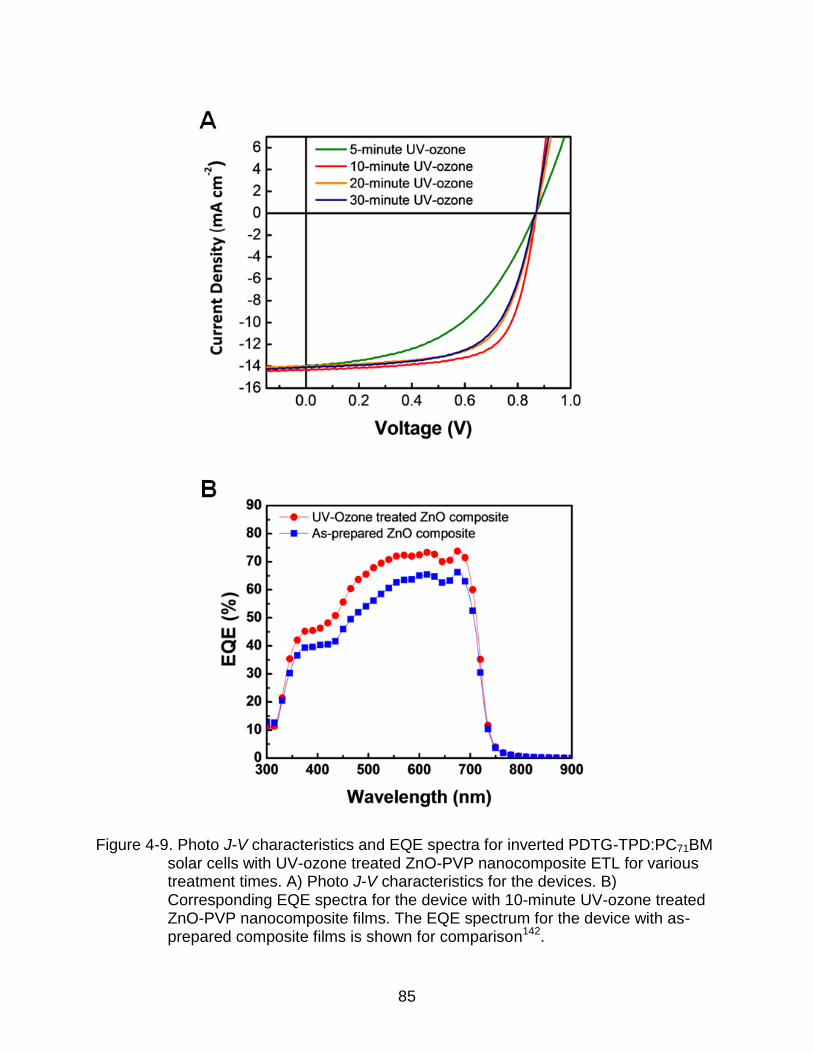
85
Figure 4-9. Photo J-V characteristics and EQE spectra for inverted PDTG-TPD:PC71BM solar cells with UV-ozone treated ZnO-PVP nanocomposite ETL for various treatment times. A) Photo J-V characteristics for the devices. B) Corresponding EQE spectra for the device with 10-minute UV-ozone treated ZnO-PVP nanocomposite films. The EQE spectrum for the device with as-prepared composite films is shown for comparison142.
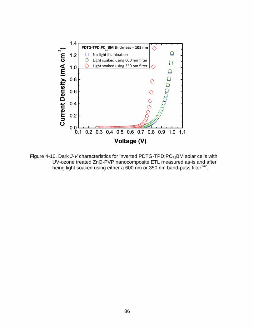
86
Figure 4-10. Dark J-V characteristics for inverted PDTG-TPD:PC71BM solar cells with UV-ozone treated ZnO-PVP nanocomposite ETL measured as-is and after being light soaked using either a 600 nm or 350 nm band-pass filter142.

87
Figure 4-11. Certified I-V characteristics for an inverted PDTG-TPD:PC71BM solar cell with 10-minute UV-ozone treated ZnO-PVP nanocomposite ETL. The device was certified by NEWPORT Corporation142.

88
Figure 4-12. Solar cell parameters versus time for encapsulated inverted PDTG-TPD:PC71BM with as-prepared and 10-minute UV-ozone treated ZnO-PVP nanocomposite ETLs. A) Short-circuit current density (Jsc) vs. time. B) Fill factor (FF) vs. time. C) Power conversion efficiency (PCE) vs. time142.

89
CHAPTER 5 LOSS MECHANISMS IN THICK-FILM LOW-BANDAP POLYMER SOLAR CELLS
5.1 Introductory Remarks
Polymer BHJ solar cells, which have the potential to provide low cost energy
harvesting, are receiving much attention in research and development109,114,116,143. In
Chapter 4, inverted PDTG-TPD:PC71BM solar cells with over 8% power conversion
efficiency was demonstrated, which is crucial for demonstrating the viability of this
technology for large-scale R2R processing142,144. Despite this performance for
laboratory-scale inverted devices, the cell geometry is not the only factor determining
their compatibility for large-scale manufacturing. Another key factor for large-scale R2R
processing of polymer solar cells is the active layer thickness required to ensure high
manufacturing yields in the PV modules145. Most high efficiency laboratory-scale
devices have an active layer that is too thin for large-scale R2R processing. Krebs and
coworkers have shown that polymer:fullerene active layers deposited by slot-die coating
have a high surface roughness and non-uniform film thickness due to the large
difference between the wet film thickness and dry film thickness145. This high surface
roughness and non-uniform film thickness for the active layer leads to a lower yield of
serially-connected polymer solar cells. To address this issue, a larger solid
concentration of polymer and fullerene is used in solution. As a result, the active layer
film thickness for the R2R processed PV module is typically around 200 nm, which is
larger than the film thickness employed in optimized laboratory-scale polymer solar
cells. Therefore, obtaining high efficiency devices with active layers thicker than 200 nm
is critical for commercialization115,145.

90
In addition to the thickness requirement associated with large-scale R2R
processing, increased active layer thickness is also required for optimal light harvesting
to produce high efficiency polymer solar cells. Presently, solar cells with enhanced light
absorption have been demonstrated by employing low bandgap polymers with optical
bandgap between 1.2 and 1.7 eV95,101,113,146,147. To obtain a high FF in these high
efficiency cells, with the exception of poly(3-hexylthiophene) (P3HT) BHJ solar cells, the
active layer used is typically less than 100 nm. However, due to optical interference
effects, a high EQE can only be obtained in these devices when the thickness exceeds
200 nm148. Therefore, despite their high power conversion efficiencies (PCEs), low
bandgap polymer solar cells do not take advantage of the true light harvesting potential
of the polymer used in such thin-film devices. The average EQE is expected to increase
for solar cells with a thicker active layer due to enhanced light absorption and optimum
optical interference. Therefore, to meet the large-scale R2R processing requirement
and ultimately realize optimum light absorption, high efficiency polymer solar cells with a
thicker active layer must be demonstrated.
In the past, demonstrating high efficiency polymer solar cells with a thick active
layer has been a challenge. Previous work has focused on obtaining high hole mobilities
in low bandgap polymers when blended with fullerene. This has been achieved by
developing novel polymer structural designs and by improving the nanoscale
morphology of polymer:fullerene BHJ films149,150. The improved carrier transport helps
alleviate the buildup of photogenerated carriers in devices with thicker active layer,
which decreases the probability of carrier recombination and, consequently, enhances
the carrier collection efficiency149-154. While this approach has been successful for
91
polymer solar cells such as poly(3-hexylthiophene):[6,6]-phenyl-C61 butyric acid methyl
ester (P3HT:PC61BM), solar cells employing low bandgap conjugated polymers with
fused donor–acceptor moieties show significant reductions in FF and PCE with
increasing the BHJ film thickness despite showing record efficiencies for thin-film
devices117,155,156. Minimizing this FF reduction and, consequently, achieving high
efficiency in low bandgap polymer solar cells with thicker active layer is particularly
important for the development of low-cost, high efficiency polymer solar cell for
commercial application.
In this chapter, the thickness dependence of the efficiency in polymer solar cells
employing the low-bandgap polymer PDTG-TPD is studied101. Previous work reported
that the PCEs of these cells can be as high as 8.1% with an active layer thickness of
about 100 nm142,144. Increasing the active layer thickness (L) up to 200 nm yielded
devices with a PCE above 8.0%, which shows the viability of the PDTG-TPD:[6,6]-
phenyl-C71 butyric acid methyl ester (PC71BM) system for large-scale R2R processing.
For devices with an active layer thickness > 200 nm, a marked reduction in FF and PCE
were observed. On the contrary, similar P3HT:PC61BM polymer solar cells showed
almost no reduction in FF for devices with active layer thickness up to 453 nm.
Interestingly, similar space-charge-limited (SCL) hole mobility values were obtained for
both polymer:fullerene BHJ films despite the difference in fill factor behavior with
increasing active layer thickness. These results are interpreted as follows: the broader
absorption band for the PDTG-TPD:PC71BM system leads to increased charge carrier
generation and increased space-charge buildup in the photoactive layer compared to
P3HT:PC61BM. The onset of space charge accumulation coincides with increased
92
carrier recombination loss in the photoactive layer, which results in a significant FF
reduction in devices with thicker active layer150. Analysis on the incident light intensity
dependence of the FF, as well as an analysis of SCL photocurrent in PDTG-
TPD:PC71BM solar cells further support this hypothesis157. In addition to space-charge
effects, the reduced FF observed in thick PDTG-TPD:PC71BM solar cells is also
attributed to a low carrier lifetime as compared to similar P3HT:PC61BM devices.
Overall, these results indicate that recombination loss due to space-charge effects and
low carrier lifetime limits the performance of thick film low-bandgap polymer solar cells.
5.2 Experimental Details
5.2.1 Device Fabrication
The detailed synthesis, purification, and polymer characterization for PDTG-TPD
has been reported in the work by Amb and coworkers101. P3HT was purchased from
Rieke Metals, Inc. Both PC61BM and PC71BM used for solar cell fabrication were
purchased from Solenne. For the inverted PDTG-TPD-based devices, the polymer and
PC71BM were dissolved in chlorobenzene with 1:1.5 weight ratio and 5% volume ratio of
1,8-diiodooctane (DIO) was added as a processing additive to both solutions. The ZnO-
PVP nanocomposite electron transporting layer, whose solution processing was
discussed in Chapter 4, was spin-cast on indium tin oxide (ITO)-coated glass
substrates. The ITO substrates were first cleaned with detergent, ultrasonicated in DI
water, acetone, and isopropyl alcohol, and subsequently dried via N2. The polymer-
fullerene solutions were then spin-coated at various spin speeds to control active layer
thickness and the resulting films were annealed at 80 oC for 30 minutes. Finally, thin
films of MoO3 (4 nm) and Ag (100 nm) were deposited through shadow masks via
thermal evaporation. The active area of the device was 4.6 mm2. For the P3HT:PC61BM

93
solar cells, P3HT and PC61BM were dissolved in chlorobenzene with 1:1 (8 mg mL-1:12
mg mL-1) weight ratio. Thermally evaporated films of MoO3 (Sigma Aldrich, 4 nm) and
bathocuproine (BCP, 5 nm) were used for the anode and cathode interlayers,
respectively. The active layer thickness was controlled by varying the spin-coating
speed. Hole-only devices were fabricated to extract the space-charge limited hole
mobility. The device structures for the polymer solar cells and hole-only devices
fabricated in this chapter is shown in Figure 5-1.
5.2.2 Device Characterization
Current density-voltage measurements were carried out in air after encapsulation
using a Keithley 4200 semiconductor system. For light intensity-dependent J-V
measurements, neutral density filters were used to control the incident light intensity
from the AM 1.5G solar simulator. For field-dependent EQE measurements, a bias was
applied to the device using a current amplifier. For all EQE measurements, the beam
spot used was smaller than the device area to ensure accuracy of the measurement.
5.3 Results and Discussions
5.3.1 PDTG-TPD:PC71BM Solar Cell Performance
Figure 5-2 shows the photocurrent density–voltage (J-V) characteristics and the
corresponding external quantum efficiency (EQE) spectra for inverted PDTG-
TPD:PC71BM solar cells with 105 nm, 204 nm, and 258 nm-thick active layers. The
short-circuit current density (Jsc) for the solar cells increases with increasing active layer
thickness due to enhanced light absorption, with the highest Jsc of 16.1 mA cm-2
obtained for the device with an active layer thickness of 258 nm. The integrated current
density from the EQE spectra, shown in Figure 5-2, is consistent with the measured Jsc
with only 5% deviation. The difference in the EQE spectra is due to the optical
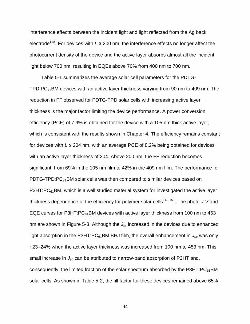
94
interference effects between the incident light and light reflected from the Ag back
electrode148. For devices with L ≥ 200 nm, the interference effects no longer affect the
photocurrent density of the device and the active layer absorbs almost all the incident
light below 700 nm, resulting in EQEs above 70% from 400 nm to 700 nm.
Table 5-1 summarizes the average solar cell parameters for the PDTG-
TPD:PC71BM devices with an active layer thickness varying from 90 nm to 409 nm. The
reduction in FF observed for PDTG-TPD solar cells with increasing active layer
thickness is the major factor limiting the device performance. A power conversion
efficiency (PCE) of 7.9% is obtained for the device with a 105 nm thick active layer,
which is consistent with the results shown in Chapter 4. The efficiency remains constant
for devices with L ≤ 204 nm, with an average PCE of 8.2% being obtained for devices
with an active layer thickness of 204. Above 200 nm, the FF reduction becomes
significant, from 69% in the 105 nm film to 42% in the 409 nm film. The performance for
PDTG-TPD:PC71BM solar cells was then compared to similar devices based on
P3HT:PC61BM, which is a well studied material system for investigated the active layer
thickness dependence of the efficiency for polymer solar cells149,151. The photo J-V and
EQE curves for P3HT:PC61BM devices with active layer thickness from 100 nm to 453
nm are shown in Figure 5-3. Although the Jsc increased in the devices due to enhanced
light absorption in the P3HT:PC61BM BHJ film, the overall enhancement in Jsc was only
~23–24% when the active layer thickness was increased from 100 nm to 453 nm. This
small increase in Jsc can be attributed to narrow-band absorption of P3HT and,
consequently, the limited fraction of the solar spectrum absorbed by the P3HT:PC61BM
solar cells. As shown in Table 5-2, the fill factor for these devices remained above 65%
95
despite increasing the thickness from 100 nm to 453 nm. This is in stark contrast to the
results obtained for the PDTG-TPD:PC71BM solar cells. The high FF obtained for these
devices is characteristic of the balanced e and h mobility in the active layer, as well as
the ability to efficiently extract photogenerated charge carriers. The low rate of hole
generation in the thick-film P3HT:PC61BM solar cells, as indicated by the small
enhancement in Jsc, helps to prevent space-charge from accumulating within the active
layer. The average FF and average EQE versus active layer thickness for both PDTG-
TPD:PC71BM and P3HT:PC61BM solar cells is summarized in Figure 5-4. Here,
‘average EQE’ refers to external quantum efficiency for the solar cell averaged over the
wavelength range corresponding to the EQE spectra. For PDTG-TPD solar cells, a high
average FF can only be obtained for devices with L ≤ 204 nm. n contrast, a FF ≥ 65%
was observed for P3HT:PC61BM solar cells with L ≤ 453 nm. n terms of the average
EQE, only thick-film PDTG-TPD:PC71BM solar cells with L ≥ 204 nm was capable of
reaching an average EQE of 65%.
In previous work, the reduction in FF for thick-film devices was attributed to
polymer solar cells with low carrier mobility such as MDMO-PPV:PC61BM150. The low
mobility increases the chances of carrier recombination and therefore reduces the FF.
To confirm that low carrier mobility was not responsible for the reduction in FF, the SCL
hole mobility was extracted from J-V measurements for PDTG-TPD:PC71BM single-
carrier devices using the Mott-Gurney Law outlined in Chapter 2 and compared those
values with the mobility values for P3HT:PC61BM solar cells (see Figure 5-5). The hole
mobility values for the 105 nm and 409 nm-thick PDTG-TPD:PC71BM devices were
3.4×10⁻³ cm2 V-1 s-1 and 2.3×10⁻³ cm2 V-1 s-1, respectively. These values are comparable
96
with hole mobility values found for optimized P3HT:PC61BM solar cells reported in the
literature149,150. It suggests that the reduction in device performance in PDTG-
TPD:PC71BM solar cells is not due to the mobility since both PDTG-TPD and P3HT
have the same mobilities.
To determine the root cause for the reduction in FF observed in thick-film PDTG-
TPD:PC71BM solar cells, the EQE spectra for the thin-film and thick-film devices were
measured under different values of internal electric field158. Figure 5-6 shows the field-
dependent EQE spectra for devices with 105 nm, 204 nm, 258 nm, and 409 nm-thick
active layer, respectively. Here, the internal electric field (E) was approximated as
. For devices an active layer thickness ≤ 204 nm, increasing the applied
field from 20 kV cm-1 to 70 kV cm-1 leads to a uniform enhancement in EQE across the
entire spectral range. The increased applied field enhances the extraction of
photogenerated charges equally across the EQE spectrum. Interestingly, for devices
with L > 204 nm, a stronger field-dependent enhancement in EQE is observed in the
spectral range from 500 to 750 nm when the applied field is increased from 20 kV cm-1
to 70 kV cm-1. This wavelength range corresponds to the absorption spectrum for
pristine PDTG-TPD films101. For devices with thick active layer, the build-up of carriers
in PDTG-TPD:PC71BM will hinder charge collection and contribute to the fill factor
reduction in thick solar cell.
As a result of the limited charge collection observed for thick-film PDTG-TPD solar
cells measured at low field, we expect the photocurrent to be reduced in this field
regime. Figure 5-7 shows the normalized photocurrent density−electric field (JL−E)
curves for PDTG-TPD:PC71BM solar cells with increasing active layer thickness. For
97
inverted PDTG-TPD:PC71BM solar cells with thickness ≤ 204 nm, the shapes of the
JL−E curves are identical. In this thickness regime, the internal electric field effectively
extracts photogenerated charges from the active layer. For inverted devices with L >
204 nm, a change in the JL−E profile is observed. In this thickness regime, a reduction
in photocurrent is observed in the low field regime. The internal electric field is no longer
able to efficiently extract photogenerated charges out of the active layer. Based on this
result, the reduced fill factor observed in PDTG-TPD:PC71BM solar cells with thicker
active layer can be attributed to two factors: (1) the reduction in internal electric field due
to increased active layer thickness L, and (2) the reduced photocurrent at low electric
field due to limited charge collection. The results in Figures 5-6 and 5-7 provide
evidence that space-charge accumulation contributes to the limited charge collection
and reduced fill factor observed in thick-film PDTG-TPD:PC71BM solar cells.
Furthermore, increased recombination loss in thick-film devices is expected since
carriers have to traverse a longer distance to be collected. To better understand the loss
mechanisms in thick-film low-bandgap polymer solar cells, a detailed study on space-
charge limited (SCL) and recombination limited photocurrent is presented herein.
5.3.2 Loss Mechanisms in Thick-Film PDTG-TPD:PC71BM Solar Cells
In comparing P3HT and PDTG-TPD, a significant difference between these two
polymers is the broader absorption spectra in PDTG-TPD due to its lower optical
bandgap (Egap ≈ 1.7 eV)101. The UV-visible-NIR absorption spectra for P3HT:PC61BM
and PDTG-TPD:PC71BM solar cells along with the photon flux for an AM 1.5G solar
spectrum are shown in Figure 5-8. From the solar spectrum, an integrated photon flux of
1.6×1017 cm-2 s-1 is obtained for a wavelength range of 400 nm – 800 nm. A larger
fraction of this photon flux is absorbed by PDTG-TPD compared to the P3HT due to its
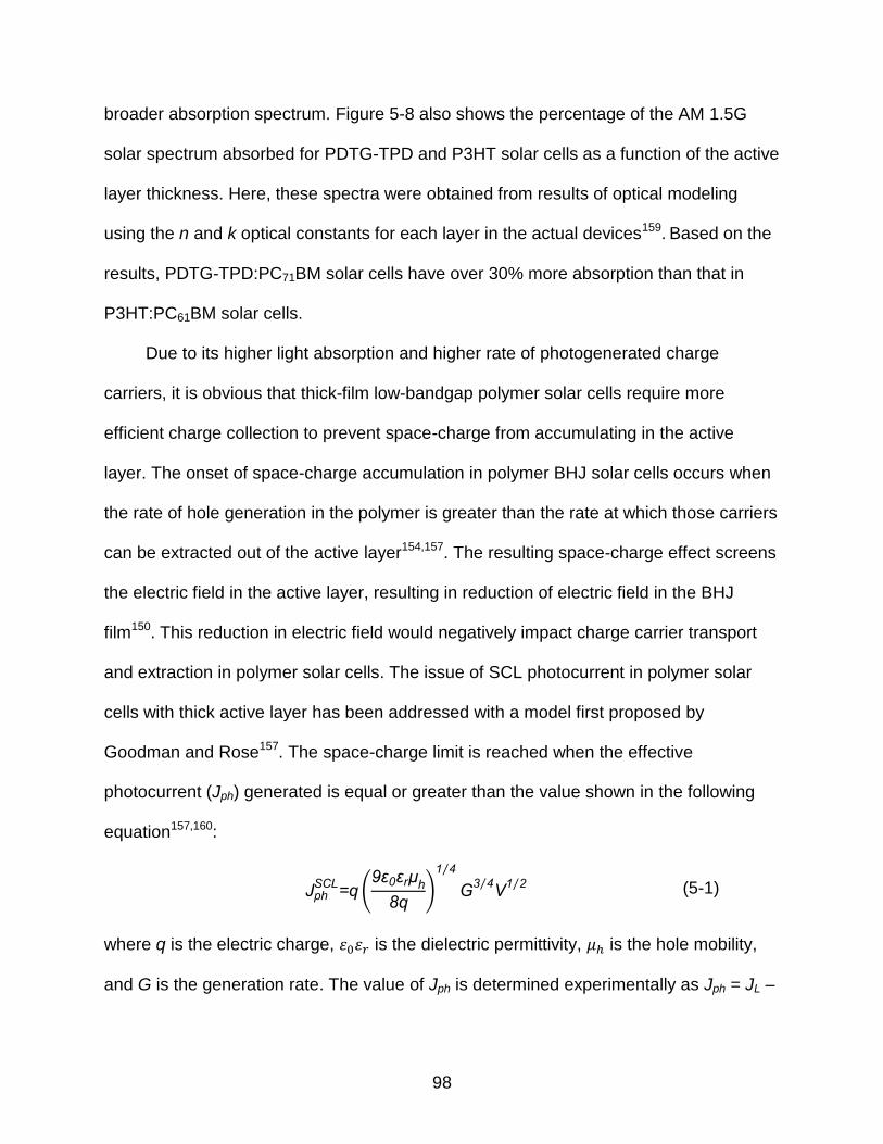
98
broader absorption spectrum. Figure 5-8 also shows the percentage of the AM 1.5G
solar spectrum absorbed for PDTG-TPD and P3HT solar cells as a function of the active
layer thickness. Here, these spectra were obtained from results of optical modeling
using the n and k optical constants for each layer in the actual devices159. Based on the
results, PDTG-TPD:PC71BM solar cells have over 30% more absorption than that in
P3HT:PC61BM solar cells.
Due to its higher light absorption and higher rate of photogenerated charge
carriers, it is obvious that thick-film low-bandgap polymer solar cells require more
efficient charge collection to prevent space-charge from accumulating in the active
layer. The onset of space-charge accumulation in polymer BHJ solar cells occurs when
the rate of hole generation in the polymer is greater than the rate at which those carriers
can be extracted out of the active layer154,157. The resulting space-charge effect screens
the electric field in the active layer, resulting in reduction of electric field in the BHJ
film150. This reduction in electric field would negatively impact charge carrier transport
and extraction in polymer solar cells. The issue of SCL photocurrent in polymer solar
cells with thick active layer has been addressed with a model first proposed by
Goodman and Rose157. The space-charge limit is reached when the effective
photocurrent (Jph) generated is equal or greater than the value shown in the following
equation157,160:
ε ε
(5-1)
where q is the electric charge, is the dielectric permittivity, is the hole mobility,
and G is the generation rate. The value of Jph is determined experimentally as Jph = JL –
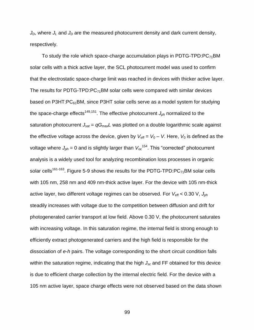
99
JD, where JL and JD are the measured photocurrent density and dark current density,
respectively.
To study the role which space-charge accumulation plays in PDTG-TPD:PC71BM
solar cells with a thick active layer, the SCL photocurrent model was used to confirm
that the electrostatic space-charge limit was reached in devices with thicker active layer.
The results for PDTG-TPD:PC71BM solar cells were compared with similar devices
based on P3HT:PC61BM, since P3HT solar cells serve as a model system for studying
the space-charge effects149,151. The effective photocurrent Jph normalized to the
saturation photocurrent Jsat = qGmaxL was plotted on a double logarithmic scale against
the effective voltage across the device, given by Veff = V0 – V. Here, V0 is defined as the
voltage where Jph = 0 and is slightly larger than Voc154. This “corrected” photocurrent
analysis is a widely used tool for analyzing recombination loss processes in organic
solar cells161-163. Figure 5-9 shows the results for the PDTG-TPD:PC71BM solar cells
with 105 nm, 258 nm and 409 nm-thick active layer. For the device with 105 nm-thick
active layer, two different voltage regimes can be observed. For Veff < 0.30 V, Jph
steadily increases with voltage due to the competition between diffusion and drift for
photogenerated carrier transport at low field. Above 0.30 V, the photocurrent saturates
with increasing voltage. In this saturation regime, the internal field is strong enough to
efficiently extract photogenerated carriers and the high field is responsible for the
dissociation of e-h pairs. The voltage corresponding to the short circuit condition falls
within the saturation regime, indicating that the high Jsc and FF obtained for this device
is due to efficient charge collection by the internal electric field. For the device with a
105 nm active layer, space charge effects were not observed based on the data shown
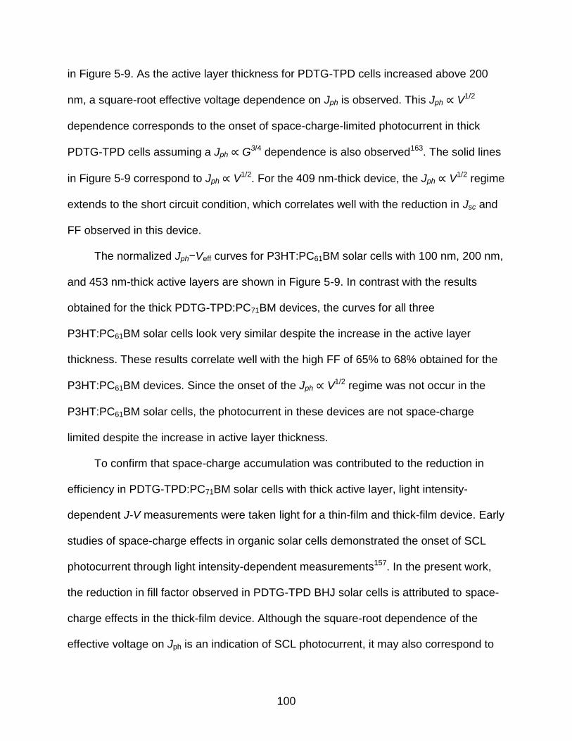
100
in Figure 5-9. As the active layer thickness for PDTG-TPD cells increased above 200
nm, a square-root effective voltage dependence on Jph is observed. This Jph V1/2
dependence corresponds to the onset of space-charge-limited photocurrent in thick
PDTG-TPD cells assuming a Jph G3/4 dependence is also observed163. The solid lines
in Figure 5-9 correspond to Jph V1/2. For the 409 nm-thick device, the Jph V1/2 regime
extends to the short circuit condition, which correlates well with the reduction in Jsc and
FF observed in this device.
The normalized Jph−Veff curves for P3HT:PC61BM solar cells with 100 nm, 200 nm,
and 453 nm-thick active layers are shown in Figure 5-9. In contrast with the results
obtained for the thick PDTG-TPD:PC71BM devices, the curves for all three
P3HT:PC61BM solar cells look very similar despite the increase in the active layer
thickness. These results correlate well with the high FF of 65% to 68% obtained for the
P3HT:PC61BM devices. Since the onset of the Jph V1/2 regime was not occur in the
P3HT:PC61BM solar cells, the photocurrent in these devices are not space-charge
limited despite the increase in active layer thickness.
To confirm that space-charge accumulation was contributed to the reduction in
efficiency in PDTG-TPD:PC71BM solar cells with thick active layer, light intensity-
dependent J-V measurements were taken light for a thin-film and thick-film device. Early
studies of space-charge effects in organic solar cells demonstrated the onset of SCL
photocurrent through light intensity-dependent measurements157. In the present work,
the reduction in fill factor observed in PDTG-TPD BHJ solar cells is attributed to space-
charge effects in the thick-film device. Although the square-root dependence of the
effective voltage on Jph is an indication of SCL photocurrent, it may also correspond to
101
recombination-limited photocurrent. In the case of recombination-limited photocurrent,
the recombination of charge carriers becomes significant since the mean free electron
or hole drift length becomes less than the active layer thickness163,164. Since
recombination-limited photocurrent is give by:
(5-2)
where is the lifetime of free carriers, it is possible to determine whether space-charge-
limited or recombination-limited photocurrent is limiting the fill factor of the solar cell by
analyzing the light intensity dependence of the photocurrent163,164. While the SCL
photocurrent scales with a 3/4 power dependence on light intensity (Eq. 1), the
photocurrent scales linearly in the absence of space-charge effects (Eq. 2).
The dependence of Jph and fill factor on incident light intensity (P0) was plotted for
the 105 nm and 409 nm-thick PDTG-TPD:PC71BM solar cells (see Figure 5-10). Neutral
density filters were used to control the incident light intensity, which was varied from
11.4 to 100 mW cm-2. The Jph−P0 data for the thin and thick PDTG-TPD:PC71BM
devices, shown in Figure 5-10, was extracted from the Jph−Veff curves shown in the
same figure. For the solar cell with a 105 nm-thick active layer, Jph showed a linear
dependence on light intensity with the slope of the linear fit to the data equal to 1.09. In
contrast, a slope of 0.77 is observed for the 409 nm-thick PDTG-TPD solar cell. The
~3/4 power dependence of Jph on the incident light intensity confirms the occurrence of
SCL photocurrent in PDTG-TPD:PC71BM solar cells at low bias. The dependence of the
saturation of the saturation voltage (Vsat) on incident light intensity provides further
evidence, in which a slope of 0.50 is extracted from the Vsat−P0 data157,163. To form a
more clear physical picture, the light-intensity dependence of the fill factor was also
102
analyzed and plotted in Figure 5-10. The fill factor remained relatively constant with
decreasing incident light intensity for the 105 nm-thick solar cell, which is expected
since the device is not space-charge-limited at P0 = 100 mW cm-2 and the thickness is
sufficiently thin to ensure efficient charge carrier extraction. For the 409 nm-thick PDTG-
TPD solar cell, a 24% enhancement in fill factor was observed as the incident light
intensity was decreased from 100 mW cm-2 to 11.4 mW cm-2. By lowering P0 and,
consequently, reducing the generation rate of charge carriers in the thick PDTG-
TPD:PC71BM active layer, space-charge buildup was reduced. As a result, enhanced
charge carrier collection and fill factor was observed in the solar cell. Despite this
enhancement, the fill factor of the 409 nm-thick device at low light intensity does not
reach the value obtained in the 105 nm device. This result indicates that the reduced
photocurrent observed for thick-film devices, first shown in Figure 5-7, could not be
completely recovered despite lowering the incident light intensity. There is still some
degree of limited charge collection occurring in thick-film PDTG-TPD:PC71BM solar
cells.
To further understand the relationship between space-charge effects and the
increased losses observed in PDTG-TPD:PC71BM solar cells with thick active layer, a
first-principles calculation is presented for the photocurrent loss relative to short-circuit
current at low effective voltages. The short-circuit current density Jsc can be calculated
from the following:
(5-3)
where S() is the reference AM 1.5G power intensity and 1 and 2 are the wavelength
limits of the absorption spectrum of the device. The external quantum efficiency is given

103
by , where IQE is the internal quantum efficiency and the
absorption efficiency. Using the calculated from Figure 5-6 and assuming various
values of IQE (from 50 to 100%), calculated values of Jsc was obtained for PDTG-
TPD:PC71BM solar cells164. Figure 5-11 shows the number of photons absorbed in the
active layer and the corresponding Jsc versus the thickness of this layer. The
experimental results for PDTG-TPD:PC71BM solar cells are shown for comparison. The
calculated Jsc strongly agrees well with the experimental results assuming an IQE of 90
– 100%, which is in agreement with previous results demonstrating that low bandgap
polymer solar cells with IQE approaching 100% are obtainable117. The photocurrent at
low effective voltages can then be determined from the following equation165:
(5-4)
where k is Boltzmann’s constant and T is the temperature. In the low active layer
thickness regime in which
, the calculated photocurrent is given by Equation 3.
At some critical active layer thickness (Lc), the solar cell becomes space-charge-limited
(i.e.
). For devices with L ≥ Lc, the calculated photocurrent is given by Equation
1 since
.
Using this formulism, the photocurrent loss relative to Jsc for PDTG-TPD:PC71BM
solar cells, which is given as 1 – Jph/Jsc, was calculated for a low effective voltage and
plotted versus active layer thickness. This result is summarized in Figure 5-11. For this
calculation, it was assumed that the number of photons absorbed in the active layer was
equal to the generation rate, G159,166. Figure 5-11 shows the calculated photocurrent
loss before the space-charge limit was reached (
, black line), after the space-

104
charge limit is reached (
, gray line), and the photocurrent loss extracted from
the experimental data. For a given hole mobility, the calculated curves intersect when
at the critical thickness Lc (dotted line). For L ≥ Lc, the photocurrent loss in
PDTG-TPD:PC71BM solar cell significantly increases since Jph is space-charge limited.
Increasing the hole mobility in the active layer leads to a larger Lc, allowing for the active
layer thickness to be increased without substantially increasing the photocurrent loss.
These conclusions are in agreement with previous reports demonstrating that a high
hole mobility in the polymer:fullerene blend is required to maintain efficient operation in
polymer solar cells with thicker active layer149,151. The experimental photocurrent loss
was then extracted for the PDTG-TPD:PC71BM solar cells and compared to the
calculated results. The calculated photocurrent loss is comparable to the experimental
values assuming a hole mobility of 1.5×10⁻³ cm2 V-1 s-1, which is close to the hole
mobility obtained experimentally.
This theoretical model was used to predict the value of Lc for polymer solar cells
with Eg for the conjugated polymer ranging from 1.4 to 2.2 eV. To make this prediction,
it was assumed that the absorption efficiency for the polymer-fullerene blend scales
linearly with the bandgap of the polymer. Furthermore, the fraction of photons absorbed
from AM1.5G versus active layer thickness calculated for PDTG-TPD:PC71BM was used
as a reference. Based on these assumptions, the critical thickness corresponding to the
onset of SCL photocurrent was plotted versus bandgap of the polymer. This result is
shown in Figure 5-12 for polymer solar cells with increasing hole mobility. The critical
thickness Lc is linearly proportional to the bandgap of the polymer, and increases as the
hole mobility of the polymer-fullerene blend increases. Based on this result, it is clear
105
that low bandgap polymer solar cells with Eg between 1.4 and 1.7 eV are severely
limited in their active layer thickness due to the large carrier concentration generated in
these devices. For example, a hole mobility ≥ 1×10⁻³ cm2 V-1 s-1 would be required to
ensure that Lc > 200 nm. If this high hole mobility cannot be obtained in these devices,
the solar cells would show significant reductions in FF with increasing active layer
thickness156.
There are two important assumptions of the theoretical SCL photocurrent model
employed in this work. First, the SCL model assumes that since the
accumulation of slow carriers in the active layer is responsible for the space-charge limit
being reached. For polymer solar cells, SCL photocurrent was first observed in systems
with very imbalanced carrier mobilities150. In this work, SCL photocurrent was observed
for solar cells using a polymer showing high hole mobility and therefore having a smaller
carrier mobility imbalance. Nevertheless, the experimental results clearly indicate that
space-charge accumulation contributed to the reduced fill and PCE observed in thick-
film PDTG-TPD:PC71BM solar cells. Furthermore, by calculating the active layer
thickness at which ph ph
, the model predicts that the space-charge limit is reached
when L ≈ 225 nm (see Figure 5-11). This prediction correlates well with the reduced
photocurrent observed for devices with L > 200 nm. Second, the model assumes that
the loss observed in thick-film polymer solar cells is due to either SCL or recombination-
limited photocurrent. However, these two loss processes are interrelated150. It is
expected that SCL and recombination-limited photocurrent will contribute to the losses
observed in PDTG-TPD solar cells with thick active layer.

106
5.4 Concluding Remarks
To conclude, the loss mechanisms responsible for limited device performance in
thick-film PDTG-TPD:PC71BM solar cells have been investigated. For polymer solar
cells with thickness up to 200 nm, efficiencies in excess of 8.0% were obtained for
devices under AM 1.5G illumination at 100 mW cm-2. These results show that the active
layer thickness requirement inherent to large-scale R2R processing can be satisfied
while still maintaining the high power conversion efficiency, and highlights the potential
of PDTG-TPD:PC71BM polymer solar cells for large-scale manufacturing. For L > 200
nm, space-charge effects and reduced carrier lifetime limits charge collection in thick-
film devices. This limited charge collection coincides with reduced fill factor and power
conversion efficiency in thick devices. These results indicate that although high
efficiencies can be obtained in solar cells with low-bandgap conjugated donor-acceptor
polymers, the high density of photogenerated charge carriers severely limits the
performance of solar cells with a thick active layer.

107
Table 5-1. Averaged solar cell performance for inverted PDTG-TPD:PC71BM devices with various active layer thickness under initial AM 1.5G solar illumination.
Active Layer Thickness
Jsc (mA cm-2)
Jsc (EQE) (mA cm-2)
Voc (V) FF (%) PCE (%)
90 nm 12.5 +/- 0.1 12.3 0.88 +/- 0.007 68.5 +/- 0.01 7.5 +/- 0.001 105 nm 13.3 +/- 0.1 13.0 0.87 +/- 0.006 68.7 +/- 0.01 7.9 +/- 0.001 153 nm 13.5 +/- 0.1 13.5 0.86 +/- 0.007 68.1 +/- 0.01 8.0 +/- 0.001 204 nm 14.9 +/- 0.2 14.7 0.86 +/- 0.009 64.5 +/- 0.01 8.2 +/- 0.002 258 nm 16.1 +/- 0.2 16.0 0.85 +/- 0.006 54.1 +/- 0.01 7.4 +/- 0.001 409 nm 15.2 +/- 0.1 14.9 0.82 +/- 0.005 41.6 +/- 0.01 5.2 +/- 0.001
Table 5-2. Averaged solar cell performance for inverted P3HT:PC61BM devices with
various active layer thickness under initial AM 1.5G solar illumination. Active Layer Thickness
Jsc (mA/cm2) Jsc (EQE) (mA/cm2)
Voc (V) FF (%) PCE (%)
100 nm 6.1 +/- 0.23 6.4 0.62 70.4 +/- 0.1 2.7 +/- 0.12 150 nm 6.1 +/- 0.05 6.4 0.62 67.1 +/- 0.1 2.5 +/- 0.17 170 nm 7.0 +/- 0.43 7.7 0.62 72.0 +/- 0.1 3.1 +/- 0.25 200 nm 7.2 +/- 0.10 7.5 0.62 71.9 +/- 0.1 3.2 +/- 0.04 307 nm 7.6 +/- 0.25 6.4 0.58 68.7 +/-1.1 3.0 +/- 0.10 340 nm 7.6 +/- 0.04 6.7 0.58 69.0 +/- 0.5 3.1 +/- 0.10 453 nm 7.4 +/- 0.29 6.5 0.56 65.5 +/- 2.2 2.7 +/- 0.20

108
Figure 5-1. Device structure for PDTG-TPD:PC71BM solar cells, P3HT:PC61BM solar cells, and corresponding single-carrier devices studied in this work. A) Inverted PDTG-TPD:PC71BM solar cell. B) PDTG-TPD:PC71BM hole-only device. C) P3HT:PC61BM solar cell. D) P3HT:PC61BM hole-only device.

109
Figure 5-2. Photo J-V characteristics and EQE spectra for inverted PDTG-TPD:PC71BM solar cells with increasing active layer thickness. A) Photo J-V characteristics for PDTG-TPD:PC71BM solar cells with 105 nm, 204 nm, and 258 nm-thick active layer. B) Corresponding EQE spectra for the devices.
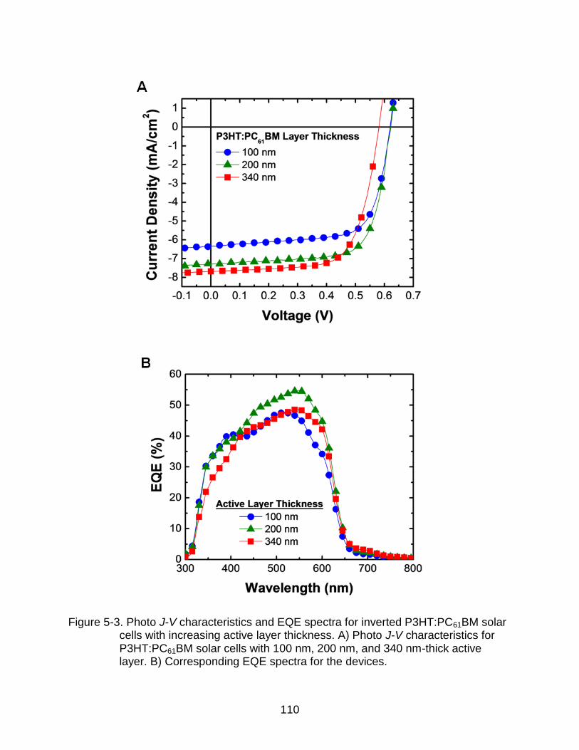
110
Figure 5-3. Photo J-V characteristics and EQE spectra for inverted P3HT:PC61BM solar cells with increasing active layer thickness. A) Photo J-V characteristics for P3HT:PC61BM solar cells with 100 nm, 200 nm, and 340 nm-thick active layer. B) Corresponding EQE spectra for the devices.
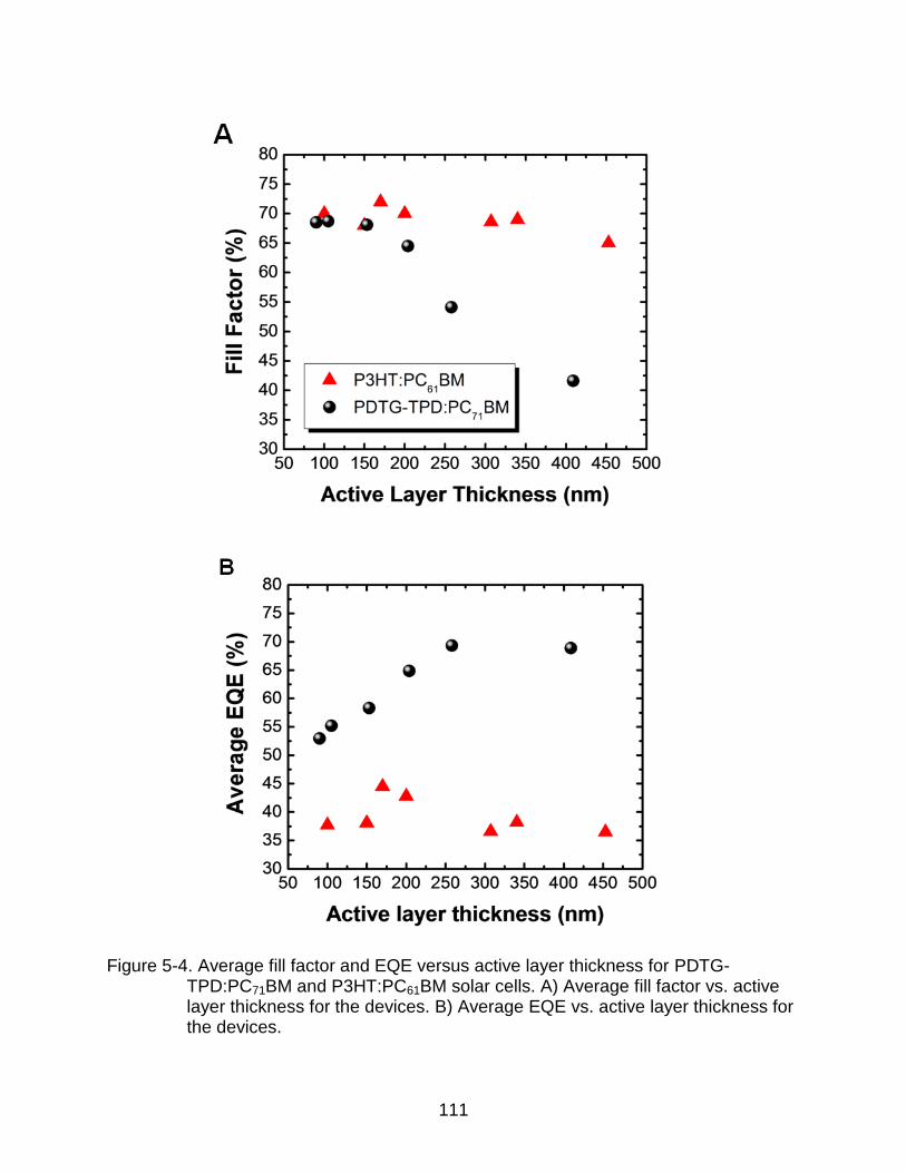
111
Figure 5-4. Average fill factor and EQE versus active layer thickness for PDTG-TPD:PC71BM and P3HT:PC61BM solar cells. A) Average fill factor vs. active layer thickness for the devices. B) Average EQE vs. active layer thickness for the devices.

112
Figure 5-5. Current density times active layer thickness (J × L) versus electric field curves for PDTG-TPD:PC71BM hole-only devices with 100 nm and 409 nm-thick layers.

113
Figure 5-6. Field-dependent EQE spectra for PDTG-TPD:PC71BM solar cells with increasing active layer thickness. A) 105 nm-thick active layer. B) 204 nm-thick active layer. C) 258 nm-thick active layer. D) 409 nm-thick active layer. The EQE spectra were measured at 20 kV cm-1 and 70 kV cm-1.
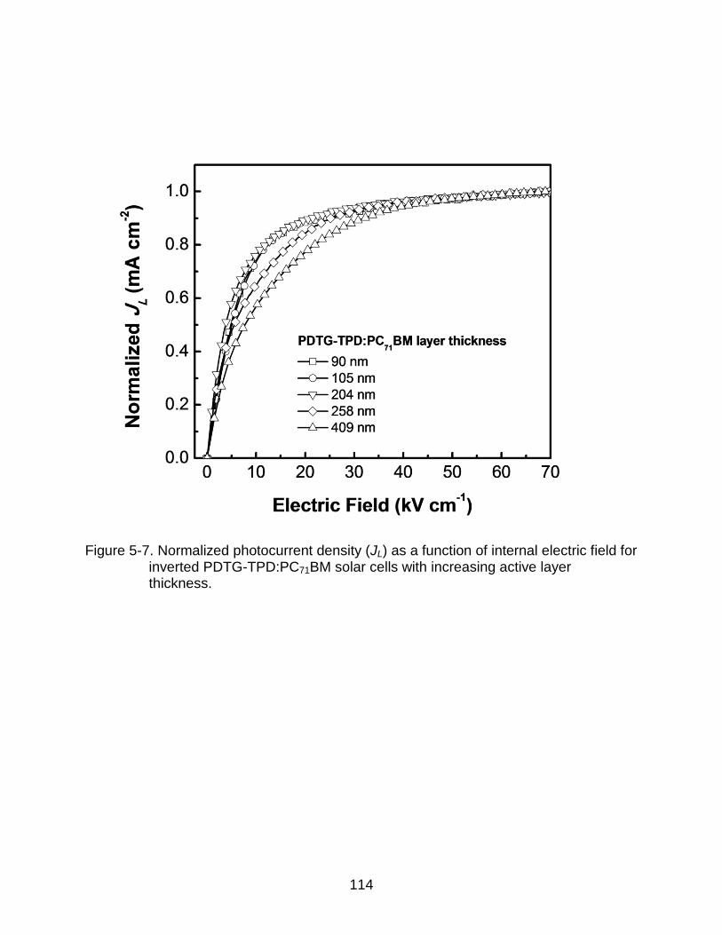
114
Figure 5-7. Normalized photocurrent density (JL) as a function of internal electric field for inverted PDTG-TPD:PC71BM solar cells with increasing active layer thickness.
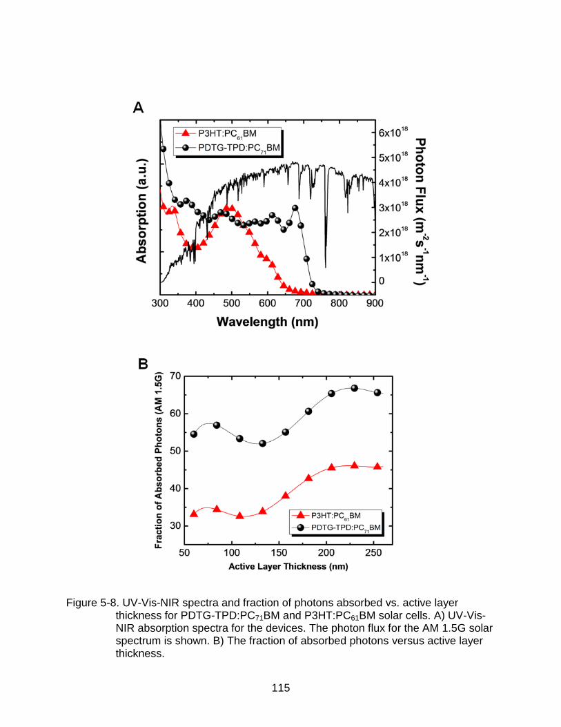
115
Figure 5-8. UV-Vis-NIR spectra and fraction of photons absorbed vs. active layer thickness for PDTG-TPD:PC71BM and P3HT:PC61BM solar cells. A) UV-Vis-NIR absorption spectra for the devices. The photon flux for the AM 1.5G solar spectrum is shown. B) The fraction of absorbed photons versus active layer thickness.

116
Figure 5-9. Normalized Jph−Veff curves for under 100 mW cm-2 illumination for PDTG-TPD:PC71BM and P3HT:PC61BM solar cells with increasing active layer thickness. A) PDTG-TPD:PC71BM cells with 105 nm, 258 nm, and 409 nm-thick layer. B) P3HT:PC61BM cells with 100 nm, 200 nm, and 453-nm thick active layer. Dashed lines highlight the value of Veff corresponding the short-circuit condition (Veff = V0). The solid lines correspond to Jph V1/2 fits of the photocurrent in the SCL regime for PDTG-TPD solar cells.

117
Figure 5-10. Light intensity dependence of the photocurrent and fill factor for 105 nm-thick and 409 m-thick PDTG-TPD:PC71BM solar cells. A) Jph-Veff curves for the 105 nm-thick device under various light intensities (from 10 to 100 mW cm-2). B) Jph-Veff curves for the 409 nm-thick device under the same light intensities. C) Jph versus light intensity for the same devices. D) Fill factor vs. light intensity for the same devices.

118
Figure 5-11. Calculated number of photons absorbed in the PDTG-TPD:PC71BM layer under AM1.5G illumination and photocurrent loss as a function of layer thickness. A) Number of photons absorbed in the photoactive layer and the corresponding short-circuit density Jsc at various IQE values vs. active layer thickness. B) Photocurrent loss relative to Jsc (1−Jph/Jsc) versus layer thickness at various hole mobility values. For this calculation, Veff = 0.4 V and
r = 4.78.

119
Figure 5-12. The critical active layer thickness corresponding to the onset of SCL photocurrent (Lc) in low bandgap polymer solar cells versus bandgap of the polymer. The calculation was performed for various values of hole mobility, ranging from 1×10⁻⁴ cm2 V-1 s-1 to 2×10⁻³ cm2 V-1 s-1.
120
CHAPTER 6 CONCLUSIONS
By inverting the device geometry of organic electronic and optoelectronic devices,
it is possible to improve the device's stability and large-scale R2R processing
compatibility. However, it is important to also demonstrate enhanced device
performance for organic electronic devices with this architecture. Early work on inverted
small-molecule and polymer LEDs showed high drive voltage due to insufficient carrier
injection. To address this problem, carrier injection for conventional and inverted organic
single-carrier devices was studied in Chapter 2. To facilitate carrier injection, electron
acceptors were used as injection layer for devices with either geometry. It was found
that inverted devices showed higher current density and injection efficiency compared to
devices with a conventional architecture. The results were confirmed by cross-
referencing steady state J-V and DI-SCLC transient measurements. The enhanced
carrier injection was attributed to a stronger degree of charge transfer between the
electron accepting injection layer and the organic semiconductor in the inverted device.
On that basis, the injection efficiency for devices with conventional structure was
enhanced by sandwiching a p-doped hole injection layer between the anode and the
organic semiconductor. Controlled doping of this interlayer allowed the injection
efficiency to be tuned. Given this result, it was understood that a strong degree of
charge transfer between the electron accepting injection layer and the organic
semiconductor was required to obtain an ohmic contact. In future work, replacing the
electron acceptors studied in this chapter with solution-processed electron accepting
interlayers is preferred for large-scale processing. However, obtaining strong charge
transfer will be required to observe ohmic injection with these new novel materials.

121
Similar to reports on inverted OLEDs, early work on inverted OPV cells showed
that the device performance was reduced when this geometry was employed. In
Chapter 4, we showed that the reduced device performance of inverted polymer
photovoltaic cells was due to limited carrier extraction by the bottom electron
transporting layer. By introducing a UV-ozone modified ZnO-polymer composite layer,
the electronic coupling between this interlayer and the photoactive layer was improved.
As a result, carrier extraction was improved and OPV cells with power conversion
efficiencies over 8% were obtained. This work illustrated the importance of carrier
selective interlayers for OPVs. Much of the research reported in the literature has
focused on employing novel carrier-selective interlayers for OPVs, such as the
water/alcohol soluble polyfluorenes used in the state-of-the-art devices. This will
continue to be an important research area for OPVs.
Lastly, in Chapter 5 the thickness dependence of the efficiency was investigated
for inverted organic photovoltaic cells. Demonstrating efficient OPV cell operation for
devices with thicker active layer is important for large-scale R2R processing. Since high
carrier mobility values were obtained in the polymer photovoltaic cells studied, it was
assumed that the active layer thickness could be extended without sacrificing the
device's performance. Power conversion efficiencies over 8% was obtained for OPV
cells with active layer thickness up to 200 nm. Increasing the active layer thickness
further significantly reduced the cell's performance. This loss was attributed to space-
charge effects in the thick photoactive layer. Future work on thick-film OPV cells should
focus on eliminating space-charge buildup in the photoactive layer.

122
LIST OF REFERENCES
1 Tse, S., Cheung, C. & So, S. in Organic Electronics: Materials, Processing, Devices and Applications (ed F. So) Ch. 3, 61-109 (CRC Press, 2009).
2 Bässler, H. Charge Transport in Disordered Organic Photoconductors a Monte
Carlo Simulation Study. physica status solidi (b) 175, 15-56, doi:10.1002/pssb.2221750102 (1993).
3 Nagase, T. & Naito, H. Localized-state distributions in molecularly doped
polymers determined from time-of-flight transient photocurrent. Journal of applied physics 88, 252-259, doi:10.1063/1.373649 (2000).
4 Salaneck, W. R., Seki, K., Kahn, A. & Pireaux, J. J. Conjugated Polymer and
Molecular Interfaces: Science and Technology for Photonic and Optoelectronic Application. (Marcel Dekker Inc., 2002).
5 Tang, C. & VanSlyke, S. Organic electroluminescent diodes. Applied Physics
Letters 51, 913-915 (1987). 6 Hofmann, S., Thomschke, M., Lüssem, B. & Leo, K. Top-emitting organic light-
emitting diodes. Optics Express 19, A1250-A1264 (2011). 7 Ikaia, M., Tokitob, S., Sakamoto, Y., Suzuki, T. & Taga, Y. Highly efficient
phosphorescence from organic light-emitting devices with an exciton-block layer. Applied Physics Letters 79, 156-158 (2001).
8 Sasabe, H. et al. High-efficiency blue and white organic light-emitting devices
incorporating a blue iridium carbene complex. Advanced Materials 22, 5003-5007 (2010).
9 Lee, T. W. et al. High-efficiency stacked white organic light-emitting diodes.
Applied Physics Letters 92, 043301 (2008). 10 Seidler, N. et al. Influence of the hole blocking layer on blue phosphorescent
organic light-emitting devices using 3, 6-di (9-carbazolyl)-9-(2-ethylhexyl) carbazole as host material. Applied Physics Letters 96, 093304 (2010).
11 Wang, Q., Deng, Z. & Ma, D. Highly efficient inverted top-emitting organic light-
emitting diodes using a lead monoxide electron injection layer. Optics Express 17, 17269-17278 (2009).
12 Chen, C. W., Lin, C. L. & Wu, C. C. An effective cathode structure for inverted
top-emitting organic light-emitting devices. Applied Physics Letters 85, 2469-2471, doi:10.1063/1.1798392 (2004).

123
13 Lee, H., Park, I., Kwak, J., Yoon, D. Y. & Lee, C. Improvement of electron injection in inverted bottom-emission blue phosphorescent organic light emitting diodes using zinc oxide nanoparticles. Applied Physics Letters 96, 153306 (2010).
14 Yun, C. et al. Electron injection via pentacene thin films for efficient inverted
organic light-emitting diodes. Applied Physics Letters 95, 053301 (2009). 15 Zhou, X. et al. Low-voltage inverted transparent vacuum deposited organic light-
emitting diodes using electrical doping. Applied Physics Letters 81, 922-924, doi:10.1063/1.1496502 (2002).
16 Krebs, F. C., Tromholt, T. & Jørgensen, M. Upscaling of polymer solar cell
fabrication using full roll-to-roll processing. Nanoscale 2, 873-886 (2010). 17 PolyIC. Laboratory Printing Machine, <http://old.poly-id.com/press-images.php>
(March 22, 2006). 18 LGBlog. LG ushers in a new era of viewing pleasure with "ultimate display"
OLED TV, <http://www.lgblog.co.uk/2012/05/oled/> (2012). 19 Reineke, S. et al. White organic light-emitting diodes with fluorescent tube
efficiency. Nature 459, 234-238 (2009). 20 Ho, P. K. H. et al. Molecular-scale interface engineering for polymer light-emitting
diodes. Nature 404, 481-484 (2000). 21 Van Slyke, S., Chen, C. & Tang, C. Organic electroluminescent devices with
improved stability. Applied Physics Letters 69, 2160 (1996). 22 Arias, A., Granström, M., Petritsch, K. & Friend, R. Organic photodiodes using
polymeric anodes. Synthetic metals 102, 953-954 (1999). 23 Kim, W. et al. Molecular organic light-emitting diodes using highly conducting
polymers as anodes. Applied Physics Letters 80, 3844-3846 (2002). 24 Choulis, S. A., Choong, V. E., Patwardhan, A., Mathai, M. K. & So, F. Interface
modification to improve hole-injection properties in organic electronic devices. Advanced Functional Materials 16, 1075 (2006).
25 Choudhury, K. R. et al. Highly Efficient Hole Injection Using Polymeric Anode
Materials for Small‐Molecule Organic Light‐Emitting Diodes. Advanced Functional Materials 19, 491-496 (2009).

124
26 Tokito, S., Noda, K. & Taga, Y. Metal oxides as a hole-injecting layer for an organic electroluminescent device. Journal of Physics D: Applied Physics 29, 2750 (1996).
27 Ding, H., Gao, Y., Small, C., Subbiah, J. & So, F. Energy level evolution of air
and oxygen exposed molybdenum trioxide films. Applied Physics Letters 96, 243307 (2010).
28 Kröger, M. et al. Role of the deep-lying electronic states of MoO3 in the
enhancement of hole-injection in organic thin films. Applied Physics Letters 95, 123301 (2009).
29 Park, S. M., Kim, Y. H., Yi, Y., Oh, H. Y. & Won Kim, J. Insertion of an organic
interlayer for hole current enhancement in inverted organic light emitting devices. Applied Physics Letters 97, 063308-063308-063303 (2010).
30 Kim, Y. K., Kim, J. W. & Park, Y. Energy level alignment at a charge generation
interface between 4, 4-bis (N-phenyl-1-naphthylamino) biphenyl and 1, 4, 5, 8, 9, 11-hexaazatriphenylene-hexacarbonitrile. Applied Physics Letters 94, 063305 (2009).
31 Zhou, X. et al. Enhanced Hole Injection into Amorphous Hole‐Transport Layers of
Organic Light‐Emitting Diodes Using Controlled p‐Type Doping. Advanced Functional Materials 11, 310-314 (2001).
32 Gao, W. & Kahn, A. Electronic structure and current injection in zinc
phthalocyanine doped with tetrafluorotetracyanoquinodimethane: Interface versus bulk effects. Organic Electronics 3, 53-63 (2002).
33 Pfeiffer, M., Forrest, S. R., Leo, K. & Thompson, M. E. Electrophosphorescent
pin organic light-emitting devices for very-high-efficiency flat-panel displays. Advanced Materials 14, 1633-1636 (2002).
34 Chang, C. C., Hsieh, M. T., Chen, J. F., Hwang, S. W. & Chen, C. H. Highly
power efficient organic light-emitting diodes with a p-doping layer. Applied Physics Letters 89, 253504 (2006).
35 Kröger, M. et al. P-type doping of organic wide band gap materials by transition
metal oxides: A case-study on Molybdenum trioxide. Organic Electronics 10, 932-938 (2009).
36 Ma, J. et al. Highly power efficient organic light-emitting diodes based on Cs2CO3
n-doped and MoO3 p-doped carrier transport layers. Semiconductor science and technology 24, 035009 (2009).

125
37 Drechsel, J., Pfeiffer, M., Zhou, X., Nollau, A. & Leo, K. Organic Mip-diodes by p-doping of amorphous wide-gap semiconductors: CV and impedance spectroscopy. Synthetic Metals 127, 201-205 (2002).
38 Poplavskyy, D., Su, W. & So, F. Bipolar charge transport, injection, and trapping
studies in a model green-emitting polyfluorene copolymer. Journal of applied physics 98, 014501-014501-014511 (2005).
39 Cheung, C., Song, W. & So, S. Role of air exposure in the improvement of
injection efficiency of transition metal oxide/organic contact. Organic Electronics 11, 89-94 (2010).
40 Han, T. H. et al. Extremely efficient flexible organic light-emitting diodes with
modified graphene anode. Nature Photonics 6, 105-110 (2012). 41 Kabra, D., Lu, L. P., Song, M. H., Snaith, H. J. & Friend, R. H. Efficient
Single‐Layer Polymer Light‐Emitting Diodes. Advanced Materials 22, 3194-3198 (2010).
42 Adachi, C., Nagai, K. & Tamoto, N. Molecular design of hole transport materials
for obtaining high durability in organic electroluminescent diodes. Applied Physics Letters 66, 2679 (1995).
43 Tse, S., Tsang, S. & So, S. Polymeric conducting anode for small organic
transporting molecules in dark injection experiments. Journal of applied physics 100, 063708-063708-063705 (2006).
44 Cheung, C., Tsung, K., Kwok, K. & So, S. Using thin film transistors to quantify
carrier transport properties of amorphous organic semiconductors. Applied Physics Letters 93, 083307-083307-083303 (2008).
45 Murgatroyd, P. Theory of space-charge-limited current enhanced by Frenkel
effect. Journal of Physics D: Applied Physics 3, 151 (1970). 46 Ishii, H., Sugiyama, K., Ito, E. & Seki, K. Energy Level Alignment and Interfacial
Electronic Structures at Organic/Metal and Organic/Organic Interfaces. Advanced Materials 11, 605-625 (1999).
47 Kahn, A., Koch, N. & Gao, W. Electronic structure and electrical properties of
interfaces between metals and π-conjugated molecular films. Journal of Polymer Science Part B: Polymer Physics 41, 2529-2548 (2003).
48 Abkowitz, M., Facci, J. & Stolka, M. Behavior of an ideal injecting contact on a
trap-free polymer. Applied Physics Letters 63, 1892 (1993).
126
49 Campbell, A. J. et al. Transient and steady-state space-charge-limited currents in polyfluorene copolymer diode structures with ohmic hole injecting contacts. Applied Physics Letters 76, 1734 (2000).
50 Campbell, I., Smith, D., Neef, C. & Ferraris, J. Consistent time-of-flight mobility
measurements and polymer light-emitting diode current–voltage characteristics. Applied Physics Letters 74, 2809 (1999).
51 Lampert, M. A. & Mark, P. Current injection in solids. (Academic Press, 1970). 52 Kao, K. C. & Hwang, W. Electrical transport in solids: With particular reference to
organic semiconductors. (Pergamon, Oxford, 1981). 53 Tsang, S., Tse, S., Tong, K. & So, S. PEDOT: PSS polymeric conducting anode
for admittance spectroscopy. Organic Electronics 7, 474-479 (2006). 54 Parthasarathy, G., Shen, C., Kahn, A. & Forrest, S. Lithium doping of
semiconducting organic charge transport materials. Journal of applied physics 89, 4986-4992 (2001).
55 Hsu, C. M. & Wu, W. T. Improved characteristics of organic light-emitting devices
by surface modification of nickel-doped indium tin oxide anode. Applied Physics Letters 85, 840-842 (2004).
56 Han, S., Yuan, Y. & Lu, Z. H. Highly efficient organic light-emitting diodes with
metal/fullerene anode. Journal of applied physics 100, 074504 (2006). 57 Hayashi, N., Ishii, H., Ouchi, Y. & Seki, K. Examination of band bending at
buckminsterfullerene (C60)/metal interfaces by the Kelvin probe method. Journal of Applied Physics 92, 3784 (2002).
58 Helander, M., Wang, Z. & Lu, Z. in Proc. of SPIE. (ed F. So) 70510Z. 59 Kasap, S. O. Principles of Electronic Materials and Devices. 3rd edn, (McGraw-
Hill, 2006). 60 Small, C. E., Tsang, S. W., Kido, J., So, S. K. & So, F. Origin of Enhanced Hole
Injection in Inverted Organic Devices with Electron Accepting Interlayer. Advanced Functional Materials 22, 3261-3266 (2012).
61 Wienkes, L., Blackwell, C. & Kakalios, J. Electronic transport in doped mixed-
phase hydrogenated amorphous/nanocrystalline silicon thin films. Applied Physics Letters 100, 072105 (2012).

127
62 Todorov, T. K. et al. Beyond 11% efficiency: Characteristics of state-of-the-art Cu2ZnSn(S,Se)4 solar cells. Advanced Energy Materials, doi:10.1002/aenm.201200348 (2012).
63 Wada, T. et al. High-efficiency CIGS solar cells with modified CIGS surface.
Solar Energy Materials and Solar Cells 67, 305-310 (2001). 64 Ramanathan, K. et al. Properties of 19.2% efficiency ZnO/CdS/CuInGaSe2 thin-
film solar cells. Progress in Photovoltaics: Research and Applications 11, 225-230 (2003).
65 Forrest, S. Ultrathin organic films grown by organic molecular beam deposition
and related techniques. Chemical Reviews 97, 1793 (1997). 66 Steinberger, S. et al. Vacuum-processed small molecule solar cells based on
terminal acceptor-substituted low-band gap oligothiophenes. Chemical Communications 47, 1982-1984 (2011).
67 Burroughes, J. et al. Light-emitting diodes based on conjugated polymers. Nature
347, 539-541 (1990). 68 Drury, C., Mutsaers, C., Hart, C., Matters, M. & de Leeuw, D. Low-cost all-
polymer integrated circuits. Applied Physics Letters 73, 108 (1998). 69 Hebner, T., Wu, C., Marcy, D., Lu, M. & Sturm, J. Ink-jet printing of doped
polymers for organic light emitting devices. Applied Physics Letters 72, 519-521 (1998).
70 Braun, D. & Heeger, A. Visible light emission from semiconducting polymer
diodes. Applied Physics Letters 58, 1982-1984 (1991). 71 Cheng, Y. J., Yang, S. H. & Hsu, C. S. Synthesis of conjugated polymers for
organic solar cell applications. Chemical Reviews 109, 5868-5923 (2009). 72 Liang, Y. & Yu, L. Development of semiconducting polymers for solar energy
harvesting. Polymer Reviews 50, 454-473 (2010). 73 Deibel, C. et al. Energetics of excited states in the conjugated polymer poly (3-
hexylthiophene). Physical Review B 81, 085202 (2010). 74 Zhu, X. Y., Yang, Q. & Muntwiler, M. Charge-transfer excitons at organic
semiconductor surfaces and interfaces. Accounts of chemical research 42, 1779-1787 (2009).
75 Chamberlain, G., Cooney, P. & Dennison, S. Photovoltaic properties of
merocyanine solid-state photocells. Nature 289, 45-47 (1981).

128
76 Loutfy, R., Sharp, J., Hsiao, C. & Ho, R. Phthalocyanine organic solar cells:
Indium/x-metal free phthalocyanine Schottky barriers. Journal of applied physics 52, 5218 (1981).
77 Rajaputra, S., Vallurupalli, S. & Singh, V. P. Copper phthalocyanine based
Schottky diode solar cells. Journal of Materials Science: Materials in Electronics 18, 1147-1150 (2007).
78 Tang, C. Two-layer organic photovoltaic cell. Applied Physics Letters 48, 183
(1986). 79 Yu, G., Gao, J., Hummelen, J., Wudl, F. & Heeger, A. Polymer Photovoltaic
Cells: Enhanced Efficiencies via a Network of Internal Donor-Acceptor Heterojunctions. Science 270, 1789-1791 (1995).
80 Hiramoto, M., Fujiwara, H. & Yokoyama, M. Three-layered organic solar cell with
a photoactive interlayer of codeposited pigments. Applied Physics Letters 58, 1062-1064 (1991).
81 Halls, J. et al. Efficient Photodiodes from Interpenetrating Polymer Networks.
Nature 376, 498-500 (1995). 82 He, Z. et al. Enhanced power-conversion efficiency in polymer solar cells using
an inverted device structure. Nature Photonics 6, 593-597 (2012). 83 Günes, S., Neugebauer, H. & Sariciftci, N. S. Conjugated Polymer-Based
Organic Solar Cells. Chemical Reviews 107, 1324-1338 (2007). 84 Hoppe, H., Sariciftci, N. & Meissner, D. Optical constants of conjugated
polymer/fullerene based bulk-heterojunction organic solar cells. Molecular Crystals and Liquid Crystals 385, 113-119 (2002).
85 Sze, S. M. & Ng, K. K. Physics of semiconductor devices. 3rd edn, (Wiley-
interscience, 2006). 86 Shrotriya, V. et al. Accurate measurement and characterization of organic solar
cells. Advanced Functional Materials 16, 2016-2023 (2006). 87 ASTM Standard E1021, Standard Test Method for Measuring Spectral Response
for Photovoltaic Cells. 88 Fitzner, R. et al. Interrelation between crystal packing and small-molecule
organic solar cell performance. Advanced Materials 24, 675-680 (2012).

129
89 Fitzner, R. et al. Dicyanovinyl–substituted oligothiophenes: Structure-property relationships and application in vacuum-processed small molecule organic solar cells. Advanced Functional Materials 21, 897-910 (2011).
90 Blouin, N., Michaud, A. & Leclerc, M. A low-bandgap poly (2,7-carbazole)
derivative for use in high-performance solar cells. Advanced Materials 19, 2295-2300 (2007).
91 Hummelen, J. C. et al. Preparation and characterization of fulleroid and
methanofullerene derivatives. The Journal of Organic Chemistry 60, 532-538 (1995).
92 Li, G., Zhu, R. & Yang, Y. Polymer solar cells. Nature Photonics 6, 153-161
(2012). 93 Padinger, F., Rittberger, R. S. & Sariciftci, N. S. Effects of postproduction
treatment on plastic solar cells. Advanced Functional Materials 13, 85-88 (2003). 94 Ma, W., Yang, C., Gong, X., Lee, K. & Heeger, A. J. Thermally stable, efficient
polymer solar cells with nanoscale control of the interpenetrating network morphology. Advanced Functional Materials 15, 1617-1622 (2005).
95 Scharber, M. C. et al. Design rules for donors in bulk-heterojunction solar cells—
Towards 10% energy-conversion efficiency. Advanced Materials 18, 789-794 (2006).
96 Havinga, E., Ten Hoeve, W. & Wynberg, H. Alternate donor-acceptor small-band-
gap semiconducting polymers; Polysquaraines and polycroconaines. Synthetic metals 55, 299-306 (1993).
97 Zhang, Q. T. & Tour, J. M. Low optical bandgap polythiophenes by an alternating
donor/acceptor repeat unit strategy. Journal of the American Chemical Society 119, 5065-5066 (1997).
98 Peet, J. et al. Efficiency enhancement in low-bandgap polymer solar cells by
processing with alkane dithiols. Nature Materials 6, 497-500 (2007). 99 Liang, Y. et al. Development of new semiconducting polymers for high
performance solar cells. Journal of the American Chemical Society 131, 56-57 (2008).
100 Zhang, Y. et al. Conjugated polymers based on C, Si and N-bridged dithiophene
and thienopyrroledione units: synthesis, field-effect transistors and bulk heterojunction polymer solar cells. Journal of Materials Chemistry 21, 3895-3902 (2011).

130
101 Amb, C. M. et al. Dithienogermole as a fused electron donor in bulk heterojunction solar cells. Journal of the American Chemical Society 133, 10062-10065 (2011).
102 Zhu, Y., Xu, X., Zhang, L., Chen, J. & Cao, Y. High efficiency inverted polymeric
bulk-heterojunction solar cells with hydrophilic conjugated polymers as cathode interlayer on ITO. Solar Energy Materials and Solar Cells 97, 83-88 (2012).
103 He, Z. et al. Largely enhanced efficiency with a pfn/al bilayer cathode in high
efficiency bulk heterojunction photovoltaic cells with a low bandgap polycarbazole donor. Advanced Materials 23, 3086-3089 (2011).
104 Choi, H. et al. Combination of titanium oxide and a conjugated polyelectrolyte for
high-performance inverted-type organic optoelectronic devices. Advanced Materials 23, 2759-2763 (2011).
105 Krebs, F. C. Fabrication and processing of polymer solar cells: a review of
printing and coating techniques. Solar Energy Materials and Solar Cells 93, 394-412 (2009).
106 Van Mullekom, H., Vekemans, J., Havinga, E. & Meijer, E. Developments in the
chemistry and band gap engineering of donor-acceptor substituted conjugated polymers. Materials science & engineering. R, Reports 32, 1-40 (2001).
107 Shaheen, S. E., White, M. S., Olson, D. C., Kopidakis, N., Ginley, D. S. Inverted
bulk-heterojunction plastic solar cells, <http://spie.org/x14269.xml> (2007). 108 Li, G., Chu, C. W., Shrotriya, V., Huang, J. & Yanga, Y. Efficient inverted polymer
solar cells. Applied Physics Letters 88, 253503 (2006). 109 Chen, L. M., Hong, Z., Li, G. & Yang, Y. Recent progress in polymer solar cells:
manipulation of polymer:fullerene morphology and the formation of efficient inverted polymer solar cells. Advanced Materials 21, 1434-1449 (2009).
110 Chen, H. Y. et al. Polymer solar cells with enhanced open-circuit voltage and
efficiency. Nature Photonics 3, 649-653 (2009). 111 Hou, J. et al. Synthesis of a low band gap polymer and its application in highly
efficient polymer solar cells. Journal of the American Chemical Society 131, 15586-15587 (2009).
112 Hou, J., Chen, H. Y., Zhang, S., Li, G. & Yang, Y. Synthesis, characterization,
and photovoltaic properties of a low band gap polymer based on silole-containing polythiophenes and 2, 1, 3-benzothiadiazole. Journal of the American Chemical Society 130, 16144-16145 (2008).
131
113 Li, Z. et al. Alternating copolymers of cyclopenta [2, 1-b; 3, 4-b'] dithiophene and thieno [3, 4-c] pyrrole-4, 6-dione for high-performance polymer solar cells. Advanced Functional Materials 21, 3331-3336 (2011).
114 Krebs, F. C. All solution roll-to-roll processed polymer solar cells free from
indium-tin-oxide and vacuum coating steps. Organic Electronics 10, 761-768 (2009).
115 Krebs, F. C. Polymer solar cell modules prepared using roll-to-roll methods:
knife-over-edge coating, slot-die coating and screen printing. Solar Energy Materials and Solar Cells 93, 465-475 (2009).
116 Krebs, F. C., Gevorgyan, S. A. & Alstrup, J. A roll-to-roll process to flexible
polymer solar cells: model studies, manufacture and operational stability studies. Journal of Materials Chemistry 19, 5442-5451 (2009).
117 Park, S. H. et al. Bulk heterojunction solar cells with internal quantum efficiency
approaching 100&percnt. Nature Photonics 3, 297-302 (2009). 118 Yip, H. L., Hau, S. K., Baek, N. S., Ma, H. & Jen, A. K. Y. Polymer Solar Cells
That Use Self‐Assembled‐Monolayer‐Modified ZnO/Metals as Cathodes. Advanced Materials 20, 2376-2382 (2008).
119 Beek, W. J. E., Wienk, M. M., Kemerink, M., Yang, X. & Janssen, R. A. J. Hybrid
zinc oxide conjugated polymer bulk heterojunction solar cells. The Journal of Physical Chemistry B 109, 9505-9516 (2005).
120 Hau, S. K. et al. Air-stable inverted flexible polymer solar cells using zinc oxide
nanoparticles as an electron selective layer. Applied Physics Letters 92, 253301-253301-253303 (2008).
121 Guo, L. et al. Highly monodisperse polymer-capped ZnO nanoparticles:
Preparation and optical properties. Applied Physics Letters 76, 2901-2903 (2000).
122 Mahamuni, S. et al. ZnO nanoparticles embedded in polymeric matrices.
Nanostructured materials 7, 659-666 (1996). 123 Cavaleri, J. J., Skinner, D. E., Colombo Jr, D. P. & Bowman, R. M. Femtosecond
study of the size‐dependent charge carrier dynamics in ZnO nanocluster solutions. The Journal of chemical physics 103, 5378 (1995).
124 Sakohara, S., Ishida, M. & Anderson, M. A. Visible luminescence and surface
properties of nanosized ZnO colloids prepared by hydrolyzing zinc acetate. The Journal of Physical Chemistry B 102, 10169-10175 (1998).

132
125 Monticone, S., Tufeu, R. & Kanaev, A. Complex nature of the UV and visible fluorescence of colloidal ZnO nanoparticles. The Journal of Physical Chemistry B 102, 2854-2862 (1998).
126 Guo, L. et al. Synthesis and characterization of poly (vinylpyrrolidone)-modified
zinc oxide nanoparticles. Chemistry of Materials 12, 2268-2274 (2000). 127 Du, T. & Ilegbusi, O. Synthesis and morphological characterization on PVP/ZnO
nano hybrid films. Journal of materials science 39, 6105-6109 (2004). 128 Du, T., Song, H. & Ilegbusi, O. J. Sol–gel derived ZnO/PVP nanocomposite thin
film for superoxide radical sensor. Materials Science and Engineering: C 27, 414-420 (2007).
129 Singla, M., Shafeeq M, M. & Kumar, M. Optical characterization of ZnO
nanoparticles capped with various surfactants. Journal of Luminescence 129, 434-438 (2009).
130 Tang, H. et al. Gas sensing behavior of polyvinylpyrrolidone-modified ZnO
nanoparticles for trimethylamine. Sensors and Actuators B: Chemical 113, 324-328 (2006).
131 Chu, T. Y. et al. Bulk heterojunction solar cells using thieno [3, 4-c] pyrrole-4, 6-
dione and dithieno [3, 2-b: 2′, 3′-d] silole copolymer with a power conversion efficiency of 7.3%. Journal of the American Chemical Society 133, 4250-4253 (2011).
132 Subbiah, J., Hartel, M. & So, F. MoO3/poly (9, 9-dioctylfluorene-co-N-[4-(3-
methylpropyl)]-diphenylamine) double-interlayer effect on polymer solar cells. Applied Physics Letters 96, 063303 (2010).
133 Subbiah, J. et al. Combined effects of MoO3 interlayer and PC70BM on polymer
photovoltaic device performance. Organic Electronics 11, 955-958 (2010). 134 Kim, D. Y. et al. The effect of molybdenum oxide interlayer on organic
photovoltaic cells. Applied Physics Letters 95, 093304-093304-093303 (2009). 135 Ding, H., Gao, Y., Kim, D. Y., Subbiah, J. & So, F. Energy level evolution of
molybdenum trioxide interlayer between indium tin oxide and organic semiconductor. Applied Physics Letters 96, 073304-073304-073303 (2010).
136 Meyer, J., Khalandovsky, R., Görrn, P. & Kahn, A. MoO3 films spin-coated from
a nanoparticle suspension for efficient hole-injection in organic electronics. Advanced Materials 23, 70-73 (2011).
133
137 Sun, Y., Seo, J. H., Takacs, C. J., Seifter, J. & Heeger, A. J. Inverted polymer solar cells integrated with a low-temperature-annealed sol-gel-derived ZnO film as an electron transport layer. Advanced Materials 23, 1679-1683 (2011).
138 Zhang, Y. et al. X-ray photoelectron spectroscopy study of ZnO films grown by
metal-organic chemical vapor deposition. Journal of crystal growth 252, 180-183 (2003).
139 Lilliedal, M. R., Medford, A. J., Madsen, M. V., Norrman, K. & Krebs, F. C. The
effect of post-processing treatments on inflection points in current–voltage curves of roll-to-roll processed polymer photovoltaics. Solar Energy Materials and Solar Cells 94, 2018-2031 (2010).
140 Aliaga, C. et al. Sum frequency generation and catalytic reaction studies of the
removal of organic capping agents from Pt nanoparticles by UV-ozone treatment. The Journal of Physical Chemistry C 113, 6150-6155 (2009).
141 Park, J. Y., Aliaga, C., Renzas, J. R., Lee, H. & Somorjai, G. A. The role of
organic capping layers of platinum nanoparticles in catalytic activity of co oxidation. Catalysis letters 129, 1-6 (2009).
142 Small, C. E. et al. High-efficiency inverted dithienogermole-thienopyrrolodione-
based polymer solar cells. Nature Photonics 6, 115-120 (2012). 143 Hoth, C. N., Choulis, S. A., Schilinsky, P. & Brabec, C. J. High photovoltaic
performance of inkjet printed polymer: fullerene blends. Advanced Materials 19, 3973-3978 (2007).
144 Chen, S. et al. Inverted polymer solar cells with reduced interface recombination.
Advanced Energy Materials 2, 1333-1337 (2012). 145 Krebs, F. C. Roll-to-roll fabrication of monolithic large-area polymer solar cells
free from indium-tin-oxide. Solar Energy Materials and Solar Cells 93, 1636-1641 (2009).
146 Kim, J. Y. et al. Efficient tandem polymer solar cells fabricated by all-solution
processing. Science 317, 222-225 (2007). 147 Chen, S. et al. Photo-carrier recombination in polymer solar cells based on P3HT
and silole-based copolymer. Advanced Energy Materials 1, 963-969 (2011). 148 Moulé, A. J., Bonekamp, J. B. & Meerholz, K. The effect of active layer thickness
and composition on the performance of bulk-heterojunction solar cells. Journal of applied physics 100, 094503 (2006).
134
149 Mihailetchi, V. D. et al. Origin of the enhanced performance in poly (3-hexylthiophene):[6, 6]-phenyl c-butyric acid methyl ester solar cells upon slow drying of the active layer. Applied Physics Letters 89, 012107 (2006).
150 Lenes, M., Koster, L., Mihailetchi, V. & Blom, P. Thickness dependence of the
efficiency of polymer:fullerene bulk heterojunction solar cells. Applied Physics Letters 88, 243502 (2006).
151 Shrotriya, V., Yao, Y., Li, G. & Yang, Y. Effect of self-organization in
polymer/fullerene bulk heterojunctions on solar cell performance. Applied Physics Letters 89, 063505 (2006).
152 Li, G. et al. “ olvent Annealing” effect in polymer solar cells based on poly (3-
hexylthiophene) and methanofullerenes. Advanced Functional Materials 17, 1636-1644 (2007).
153 Thompson, B. C. & Fréchet, J. M. J. Polymer–fullerene composite solar cells.
Angewandte chemie international edition 47, 58-77 (2007). 154 Blom, P. W. M., Mihailetchi, V. D., Koster, L. J. A. & Markov, D. E. Device
physics of polymer:fullerene bulk heterojunction solar cells. Advanced Materials 19, 1551-1566 (2007).
155 Lee, J. K. et al. Processing additives for improved efficiency from bulk
heterojunction solar cells. Journal of the American Chemical Society 130, 3619-3623 (2008).
156 Moon, J. S., Jo, J. & Heeger, A. J. Nanomorphology of PCDTBT:PC70BM Bulk
Heterojunction Solar Cells. Advanced Energy Materials 2, 304-308 (2012). 157 Mihailetchi, V., Wildeman, J. & Blom, P. Space-charge limited photocurrent.
Physical review letters 94, 126602 (2005). 158 Mühlbacher, D. et al. High photovoltaic performance of a low-bandgap polymer.
Advanced Materials 18, 2884-2889 (2006). 159 Hoppe, H., Arnold, N., Sariciftci, N. & Meissner, D. Modeling the optical
absorption within conjugated polymer/fullerene-based bulk-heterojunction organic solar cells. Solar Energy Materials and Solar Cells 80, 105-113 (2003).
160 Goodman, A. M. & Rose, A. Double extraction of uniformly generated electron-
hole pairs from insulators with noninjecting contacts. Journal of applied physics 42, 2823 (1971).
135
161 Liu, L. & Li, G. Investigation of recombination loss in organic solar cells by simulating intensity-dependent current–voltage measurements. Solar Energy Materials and Solar Cells 95, 2557-2563 (2011).
162 Street, R., Schoendorf, M., Roy, A. & Lee, J. Interface state recombination in
organic solar cells. Physical Review B 81, 205307 (2010). 163 Choudhury, K. R. et al. Understanding the performance and loss-mechanisms in
donor–acceptor polymer based solar cells: Photocurrent generation, charge separation and carrier transport. Solar Energy Materials and Solar Cells 95, 2502-2510 (2011).
164 Lenes, M., Morana, M., Brabec, C. J. & Blom, P. W. M. Recombination-limited
photocurrents in low bandgap polymer/fullerene solar cells. Advanced Functional Materials 19, 1106-1111 (2009).
165 Sokel, R. & Hughes, R. Numerical analysis of transient photoconductivity in
insulators. Journal of applied physics 53, 7414 (1982). 166 Law, M. et al. Determining the internal quantum efficiency of PbSe nanocrystal
solar cells with the aid of an optical model. Nano letters 8, 3904-3910 (2008).

136
BIOGRAPHICAL SKETCH
Cephas Small was born in 1979 in Brooklyn, NY as the youngest of four, with two
older sisters and an older brother. He grew up in Uniondale, NY, a small suburban town
on Long Island. Throughout elementary school, junior high school and high school,
Cephas was heavily involved in activities involving creativity, self-expression, and
problem solving, such as music, math & science clubs, and sports. His first love was
music, learning to play various styles of music on the saxophone and participating in
music competitions. After graduation from high school, he received a music scholarship
from Northeastern University, where he majored in chemical engineering based on the
advice of his favorite math teacher in high school.
At Northeastern University, Cephas pursued his academic interests, continued
playing the saxophone as part of his scholarship requirements, and served as a student
leader with the National Society of Black Engineers (NSBE) on the chapter and regional
levels. As he approached graduation, his mentors encouraged him to pursue graduate
school since he excelled in coursework involving hands-on design work. At the same
time, through his involvements with NSBE, he met research faculty at Norfolk State
University and he was encouraged to apply to the university’s graduate program.
Cephas was accepted to the historic black college and began his master’s degree
thesis work after graduating from Northeastern.
At Norfolk State University, he learned how to conduct research under the tutelage
of r. Mikhail oginov at the university’s enter for Materials Research. During his time
at Norfolk State, Cephas realized that he wanted to conduct device-related research for
his doctorate studies since the majority of his research work at that time was focused on
materials characterization. After receiving his Master of Science, he joined the Materials

137
Science and Engineering Department at the University of Florida in the fall of 2006. He
was granted the opportunity to work with Professor Franky So in his Organic Electronic
Materials and Devices Laboratory. There, he learned the operating principles for various
organic electronic and optoelectronic devices. Under the direction of Dr. Franky So, he
conducted high-impact research work in the area of organic electronics.
Cephas received his doctorate in the fall of 2012. He intends to continue his
research work on the development of novel material and device design for organic
electronics.