buckminsterfullerene on kbr studied by high resolution nc ...peter/theses/burke.pdf ·...
TRANSCRIPT
Buckminsterfullerene on KBr studied byHigh Resolution NC-AFM:
Molecular nucleation and growth on aninsulator
Sarah A. BurkeDepartment of Physics
McGill UniversityAugust, 2004
A thesis submitted to McGill Universityin partial fulfilment of the requirements of the degree of MSc
c© Sarah A. Burke 2004

Contents
Abstract ix
Resume x
Acknowledgments xi
List of Abbreviations and Symbols xii
1 Introduction and Background 1
1.1 Introduction and Motivation . . . . . . . . . . . . . . . . . . . . . . . 1
1.2 Overview of Atomic Force Microscopy . . . . . . . . . . . . . . . . . . 3
1.2.1 Contact-mode atomic force microscopy . . . . . . . . . . . . . 4
1.2.2 Non-contact atomic force microscopy . . . . . . . . . . . . . . 7
1.3 Brief theory of Growth and Epitaxy . . . . . . . . . . . . . . . . . . . 12
1.3.1 Nucleation and growth concepts . . . . . . . . . . . . . . . . . 12
1.3.2 Epitaxy of organic molecules . . . . . . . . . . . . . . . . . . . 19
1.4 C60 on KBr: prototypical system . . . . . . . . . . . . . . . . . . . . 23

CONTENTS iii
2 Experimental Methods 26
2.1 The Ultra-High Vacuum system . . . . . . . . . . . . . . . . . . . . . 26
2.1.1 Description of removable elements . . . . . . . . . . . . . . . . 29
2.1.2 Description of preparation chamber instruments . . . . . . . . 33
2.1.3 Description of main imaging chamber . . . . . . . . . . . . . . 34
2.2 Description of imaging modes used . . . . . . . . . . . . . . . . . . . 39
2.2.1 Contact-mode AFM imaging . . . . . . . . . . . . . . . . . . . 39
2.2.2 Non-contact AFM imaging . . . . . . . . . . . . . . . . . . . . 42
3 KBr substrate preparation and characterization 47
3.1 Preparation of the KBr(001) surface . . . . . . . . . . . . . . . . . . . 47
3.1.1 Comparison of air-cleaved and UHV-cleaved surfaces . . . . . 50
3.2 Contact mode imaging of the KBr(001) surface . . . . . . . . . . . . 52
3.2.1 Preliminary results from variable temperature friction measure-ments . . . . . . . . . . . . . . . . . . . . . . . . . . . . . . . 52
3.2.2 Preliminary results of ESD modification of KBr by SEM . . . 54
4 C60 on KBr – imaging and growth 58
4.1 Deposition of C60 molecules on the KBr(001) surface . . . . . . . . . 58
4.2 General growth characteristics and structure . . . . . . . . . . . . . . 59
4.3 Structure determination of C60 overlayer . . . . . . . . . . . . . . . . 65
4.3.1 Structure determination from overlayer rotation angle . . . . . 66

iv CONTENTS
4.3.2 Structure determination by Image addition method . . . . . . 67
4.3.3 Model structures from image overlay and reconstruction . . . 72
4.3.4 Comparison of possible structures . . . . . . . . . . . . . . . . 74
4.4 First layer C60 – Bright and dim molecules . . . . . . . . . . . . . . . 78
4.5 Nucleation of C60 on KBr at kink sites . . . . . . . . . . . . . . . . . 80
4.5.1 Preliminary results of defect induced nucleation . . . . . . . . 84
4.6 Kelvin Probe imaging of C60 on KBr . . . . . . . . . . . . . . . . . . 87
5 Conclusions and Outlook 89
A Replacement of Laser Diode 92
B LEED of C60 on KBr(001) surface 95
C Prediction Algorithm for Molecular Epitaxy 97
D Lattice structure prediction algorithm code 100
E Code for electrostatic kink site potential calculation 105

List of Figures
1.1 Key events in Scanning Probe Microscopy: STM to now . . . . . . . 4
1.2 Comparison of contact mode AFM with reading of braille . . . . . . . 5
1.3 Schematic of a typical NC-AFM . . . . . . . . . . . . . . . . . . . . . 8
1.4 Example of frequency shift vs. distance relation showing contrast in-version . . . . . . . . . . . . . . . . . . . . . . . . . . . . . . . . . . . 11
1.5 Atomistic surface processes . . . . . . . . . . . . . . . . . . . . . . . . 13
1.6 Energetics and growth modes . . . . . . . . . . . . . . . . . . . . . . 17
1.7 Definition of epitaxial lattice parameters . . . . . . . . . . . . . . . . 21
1.8 Approximately to scale model of C60 molecules on a KBr surface . . . 25
2.1 Photograph of UHV apparatus . . . . . . . . . . . . . . . . . . . . . . 27
2.2 Plot of floor vibrations measured by accelerometer in JEOL instrumentroom . . . . . . . . . . . . . . . . . . . . . . . . . . . . . . . . . . . . 28
2.3 Crystal cleaving holder and cleaving station . . . . . . . . . . . . . . 30
2.4 Photograph of cantilever holder for AFM measurements . . . . . . . . 31
2.5 SEM image of a typical Nanosensors cantilever . . . . . . . . . . . . . 32
vi LIST OF FIGURES
2.6 Top view photograph of AFM/STM/SEM stage . . . . . . . . . . . . 35
2.7 Beam deflection optical system with quadrant photo-diode . . . . . . 36
2.8 Schematic of SEM view angles . . . . . . . . . . . . . . . . . . . . . . 38
2.9 Simplified Block diagram of frequency detection of NanoSurf PLL . . 43
2.10 Block diagram of NC-AFM imaging mode with external PLL and KPMfeedback . . . . . . . . . . . . . . . . . . . . . . . . . . . . . . . . . . 45
2.11 Illustration of Kelvin Probe imaging . . . . . . . . . . . . . . . . . . . 46
3.1 Atomic resolution with NC-AFM on KBr(001) surface – typical features 48
3.2 Defects created by electron damage on KBr(001) surface . . . . . . . 49
3.3 LEED images KBr(001) surface . . . . . . . . . . . . . . . . . . . . . 50
3.4 Comparison of air cleaved and vacuum cleaved KBr surfaces . . . . . 51
3.5 FFM images at liquid He, liquid N, and room temperature . . . . . . 53
3.6 ESD modification of KBr surface by SEM . . . . . . . . . . . . . . . 56
3.7 Ripple formation on ESD modified KBr surface . . . . . . . . . . . . 57
4.1 Temperature dependance of deposition rate . . . . . . . . . . . . . . . 59
4.2 Island appearance as a function of deposition rate and coverage . . . 61
4.3 Two layer C60 island . . . . . . . . . . . . . . . . . . . . . . . . . . . 62
4.4 Compact C60 island with incomplete top layer . . . . . . . . . . . . . 63
4.5 Comparison of C60 growth at step edge to “seaweed” growth . . . . . 64
4.6 Molecular and atomic resolution on C60 on KBr . . . . . . . . . . . . 65
4.7 Example of Image addition method of supercell determination . . . . 69

LIST OF FIGURES vii
4.8 Possible C60 on KBr supercells . . . . . . . . . . . . . . . . . . . . . . 70
4.9 Model structures from image overlay . . . . . . . . . . . . . . . . . . 72
4.10 Reconstruction of molecular resolution image and models of 8× 3 andc11× 3 supercells . . . . . . . . . . . . . . . . . . . . . . . . . . . . . 73
4.11 Girifalco potential and harmonic approximation for C60 –C60 interaction 76
4.12 First layer bright and dim C60 molecules . . . . . . . . . . . . . . . . 78
4.13 Direct observation of C60 nucleation at kink sites . . . . . . . . . . . 81
4.14 Calculated electrostatic potential at a kink site . . . . . . . . . . . . . 82
4.15 Island sizes of C60 on KBr surface with defects . . . . . . . . . . . . . 85
4.16 Kelvin Probe image of C60 on KBr (with Au deposited) . . . . . . . . 88
A.1 Schematic of laser diode assembly for AFM beam deflection system . 93
A.2 Focusing of the laser beam on the cantilever . . . . . . . . . . . . . . 94
B.1 LEED images of C60 on KBr(001) at various energies . . . . . . . . . 96

List of Tables
2.1 Manufacturer’s specifications for types of cantilevers used. . . . . . . 32
4.1 Rates and coverages of C60 on KBr samples used . . . . . . . . . . . . 60
4.2 C60 parameters for Girifalco potential and energy calculation . . . . . 75
4.3 Comparison of different possible n× 3 C60 overlayer structures . . . . 77
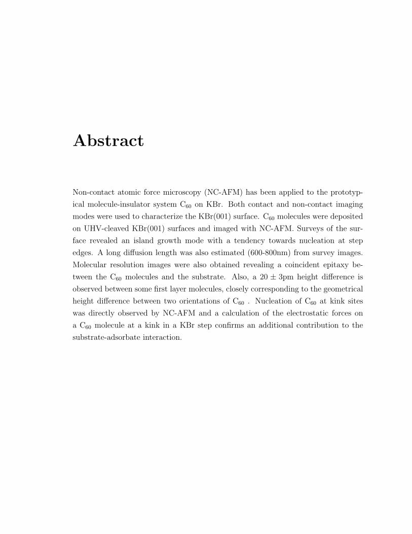
Abstract
Non-contact atomic force microscopy (NC-AFM) has been applied to the prototyp-
ical molecule-insulator system C60 on KBr. Both contact and non-contact imaging
modes were used to characterize the KBr(001) surface. C60 molecules were deposited
on UHV-cleaved KBr(001) surfaces and imaged with NC-AFM. Surveys of the sur-
face revealed an island growth mode with a tendency towards nucleation at step
edges. A long diffusion length was also estimated (600-800nm) from survey images.
Molecular resolution images were also obtained revealing a coincident epitaxy be-
tween the C60 molecules and the substrate. Also, a 20 ± 3pm height difference is
observed between some first layer molecules, closely corresponding to the geometrical
height difference between two orientations of C60 . Nucleation of C60 at kink sites
was directly observed by NC-AFM and a calculation of the electrostatic forces on
a C60 molecule at a kink in a KBr step confirms an additional contribution to the
substrate-adsorbate interaction.
Resume
La microscopie a force atomique hors-contact (NC-AFM) a ete applique a l’etude du
systeme C60 sur KBr, qui est un example d’un systeme de molecules sur substrat
isolant. Des modes en contact et hors-contact on ete utileses pour characteriser
la surface du KBr(001). Des molecules de C60 furent deposees sur une surface de
KBr(001) fendue sous UHV et furent imagees par NC-AFM. Une etude revela la
croissance d’ılots de molecules sur las surface et une tendance de nucleation aux
bords de terrasses atomique. Une grand longueur de diffusion de molecules (600–
800nm) fut estimee a partir des image obtenues. Des images a resolution moleculaire
furent obtenues et une difference de hauteur de 20 ± 3pm entre certaines molecules
de la premiere couche, ce qui correspond a la difference geometrique de hauteur entre
deux orientations de C60 . La nucleation a des sites “kink” fut observee directement
par NC-AFM, et un calcul des forces electrostatiques au site de la molecule confirme
une contribution additionelle a l’interaction entre le substrat et la molecule.

Acknowledgments
First and foremost, I would like to acknowledge my supervisor Dr. Peter Grutter for
his constant guidance, creativity and ability to inspire. Thank-you for keeping me
excited about my work, and giving me the freedom to pursue what I found interesting.
I would especially like to thank the people I worked with every day, Jeffrey Mativetsky
and Shawn Fostner, for their help in many ways, including keeping the instrument
running, the data flowing, and maintaining my sanity (mostly!). Without their as-
sistance and friendship this work would not have been possible. I would also like to
acknowledge Dr. Regina Hoffmann for helping me learn how to use the instrument,
and for giving me advice on how to proceed with my work.
I would also like to thank the other members of the group for their support, advice,
and keeping life in the lab fun. I would especially like to thank Patricia Davidson for
helping me with the translation of my abstract. In addition, I would like to thank
Dr. Martin Grant, and Dr. Roland Bennewitz for helpful discussions.
For financial support, I would like to acknowledge NSERC for funding my studies
through a postgraduate scholarship, as well as the Physics Department, the Center
for Materials Physics and my supervisor Dr. P. Grutter.
Lastly, I would like to thank the people in my life outside work. My parents, for
always encouraging me to explore the world around me and pursue what excited me.
I would especially like to thank Jeffrey LeDue for his unwavering love and support,
stimulating scientific discussions, and code de-bugging assistance!

List of Abbreviations and Symbols
AFM Atomic Force Microscopy/Microscope
CPD, VCPD Contact potential difference
C60 60 carbon cage molecule, “Buckminster Fullerene”
EFM Electrostatic Force Microscopy/Microscope
FIM Field Ion Microscopy/Microscope
LEED Low energy electron diffraction
LD Laser diode
LF-AFM/FFM Lateral-force AFM /
Friction Force Microscopy/Microscope
MFM Magnetic Force Microscopy/Microscope
NC-AFM/FM-AFM/DSFM Non-contact AFM / Frequency modulation AFM /
Dynamic Scanning Force Microscopy/Microscope
QPD Quadrant Photodiode
RHEED Reflection High Energy Electron Diffraction
SEM Secondary Electron Microscopy/Microscope
STM Scanning Tunneling Microscopy/Microscope
TEM Transmission Electron Microscopy/Microscope

xiii
A Amplitude of cantilever oscillation
ai Substrate lattice constant
bi Overlayer lattice constant
[C] Matrix describing overlayer relation to substrate lattice
cN Normal mode spring constant of cantilever
cL Lateral or torsional mode spring constant of cantilever
δf Error in frequency measurement
∆f Measured/set-point frequency shift
f0 Natural/free resonant frequency of cantilever
FN Normal force/load
FL Lateral/friction force

Chapter 1
Introduction and Background
1.1 Introduction and Motivation
The development of scanning probe microscopy as a tool for exploring a wide variety
of surface science systems has helped to open up the nanoscale world for scientific
investigation. The invention of the Scanning Tunneling Microscope in 1982 by Binnig
and Rohrer [1] has since lead to a variety of different tools for imaging, characterizing,
and even influencing the properties of surfaces and nanostructures. The field of
scanning probe microscopy (SPM) has had an influence on a wide range of fields
from biology to chemistry to physics and engineering.
One key area of study to which STM and AFM have been valuable assets, is the
study of molecules on surfaces. The ability to image, electronically probe, and ma-
nipulate molecules on surfaces has lead to a better understanding of these systems
with applications ranging from catalysis to molecular electronics. Indeed, the ability
to study these systems and control the environment of the molecule with the tip has
lead to a revival [2] of the idea of molecular electronics first proposed in 1974 by
Aviram and Ratner [3]. The pursuit of a working single molecule electronic device is
ongoing with many different approaches being explored [4].
2 Chapter 1. Introduction and Background
The construction of a planar, three-terminal molecular device would be desirable from
an integration standpoint. Since current silicon based technologies rely on planar
structures, a molecular device would be more easily integrated into current architec-
tures if a planar geometry could be achieved. However, the resistance of a molecule
∼1 nm in size is of the order of 1GΩ, which is large compared to the resistance of
a typical semiconductor on the same scale. This leads to currents running through
the substrate as well as the molecule, making the effect of the molecule on the prop-
erties of the device difficult to interpret and predict. To eliminate this problem, an
insulating surface would ideally be used in the construction of a planar molecular
device.
Additionally, the use of a planar geometry would allow the influence of the substrate
on the molecule to be studied. Effects such as charge transfer and steric hinder-
ance to conformations could be studied in a planar device where the molecule is in
direct contact with the surface. Electronic properties of two terminal devices can
be measured by STM, especially where the tip is atomically characterized by field
ion microscopy (FIM), however, only the contacts interact with the molecule in this
geometry. Similarly, break-junction experiments have been performed in electrolyte
solutions to allow gate voltages to be applied to the molecule without these substrate
interactions [5].
The design and implementation of a molecular device on an insulator would be diffi-
cult at this point in time as there is currently very little known about surface science
on insulating surfaces. The majority of traditional surface science tools, including
STM, are electron based. This makes the study of insulating surfaces difficult at best,
due to charging effects and damage caused by the measurement process. Previous
studies of molecular systems on insulating substrates have been performed using con-
tact mode AFM, TEM of released films, and/or RHEED [6, 7, 8, 9]. However, these
techniques provide either low resolution information (as in contact mode AFM), may
be destructive (as may occur with contact AFM, or electron techniques), or examine
structures which may have been altered by the process or sample preparation (as
in the case of released films which may relax from the structure on the substrate,
or the use of RHEED during growth which could create charge defects and alter
1.2 Overview of Atomic Force Microscopy 3
the growth). The addition of atomic resolution non-contact atomic force microscopy
(NC-AFM) nearly a decade ago [10, 11] to the surface science toolbox has made the
high-resolution, non-destructive, real-space imaging of insulating surfaces possible.
As this tool is developed and applied to a wider variety of systems, it has the po-
tential to provide similar information about surface surface of insulators, including
about molecular systems deposited on insulators, as STM was able to provide for
conducting surface systems [12].
As more is learned about insulating surfaces with NC-AFM, and how deposited
molecules and metals will interact with them, it may become possible to design
and implement a planar molecular device on an insulating surface. The NC-AFM
technique can then be applied to image the device with high resolution to determine
the atomic positions of the leads, molecule, and substrate. This detailed informa-
tion can then be used as input to model the device and compare to experimental
results, thus closing the loop between theory and experiment. In this way, such a de-
vice will hopefully increase our understanding of the processes involved in transport
through nanoscopic structures, contacts and molecules, as well as having potential
technological applications.
The aim of this thesis is to describe the use of NC-AFM as a tool for studying
molecular systems on insulating surfaces, as well as some of the relevant background
concepts, through the example of C60 on KBr.
1.2 Overview of Atomic Force Microscopy
Originally intended to locally probe thin oxide layers on the micron scale for IBM
corporation to improve gate oxides in transistors, the STM was instantly a much
more powerful tool than expected. Atomic resolution on Si(111)7×7 was obtained
within the first year of its reported use [13]. Atomic force microscopy (AFM) was
invented on a similar principle in 1986 by Binnig, Quate and Gerber [14], and the
development of lateral force, or friction force microscopy (LF-AFM or FFM) followed
one year later [15]. The first lattice image was obtained on graphite with contact
4 Chapter 1. Introduction and Background
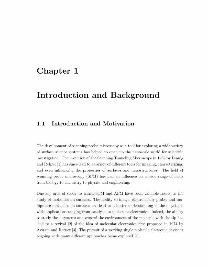
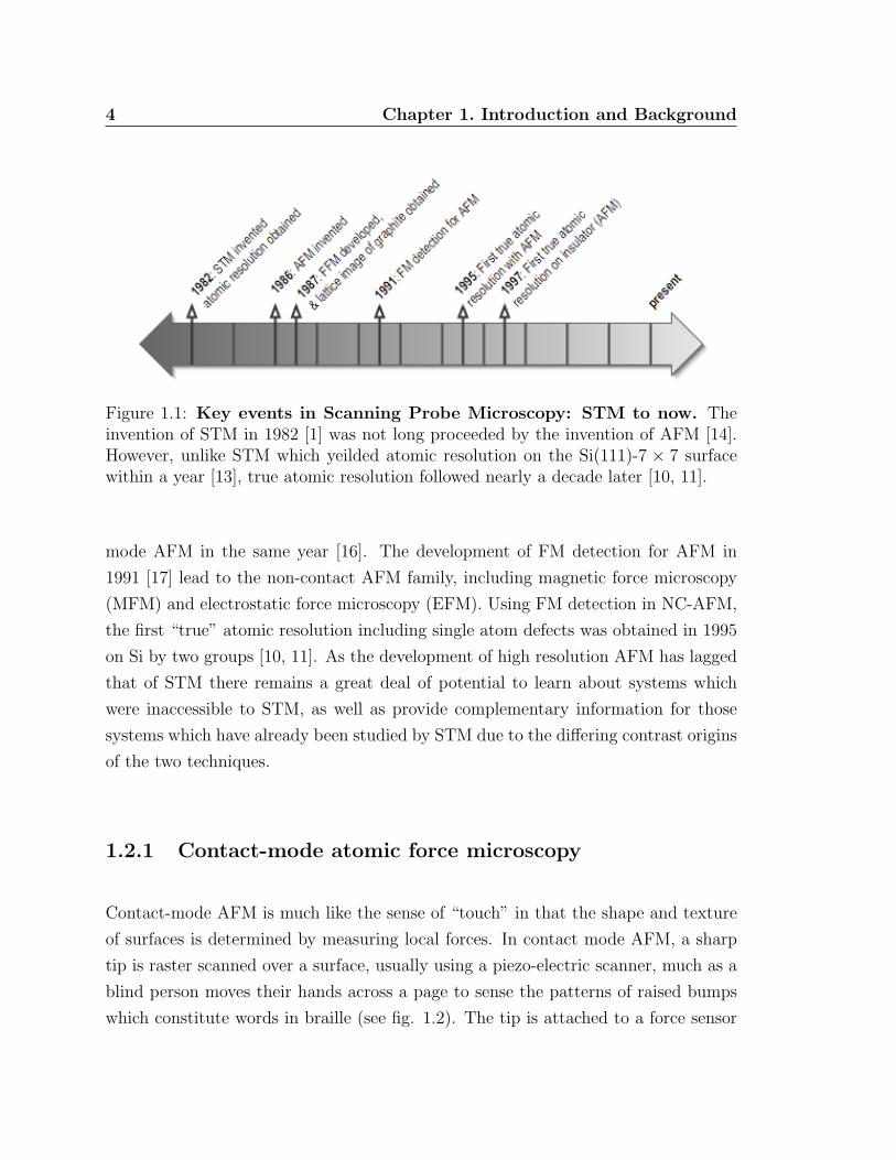
Figure 1.1: Key events in Scanning Probe Microscopy: STM to now. Theinvention of STM in 1982 [1] was not long proceeded by the invention of AFM [14].However, unlike STM which yeilded atomic resolution on the Si(111)-7 × 7 surfacewithin a year [13], true atomic resolution followed nearly a decade later [10, 11].
mode AFM in the same year [16]. The development of FM detection for AFM in
1991 [17] lead to the non-contact AFM family, including magnetic force microscopy
(MFM) and electrostatic force microscopy (EFM). Using FM detection in NC-AFM,
the first “true” atomic resolution including single atom defects was obtained in 1995
on Si by two groups [10, 11]. As the development of high resolution AFM has lagged
that of STM there remains a great deal of potential to learn about systems which
were inaccessible to STM, as well as provide complementary information for those
systems which have already been studied by STM due to the differing contrast origins
of the two techniques.
1.2.1 Contact-mode atomic force microscopy
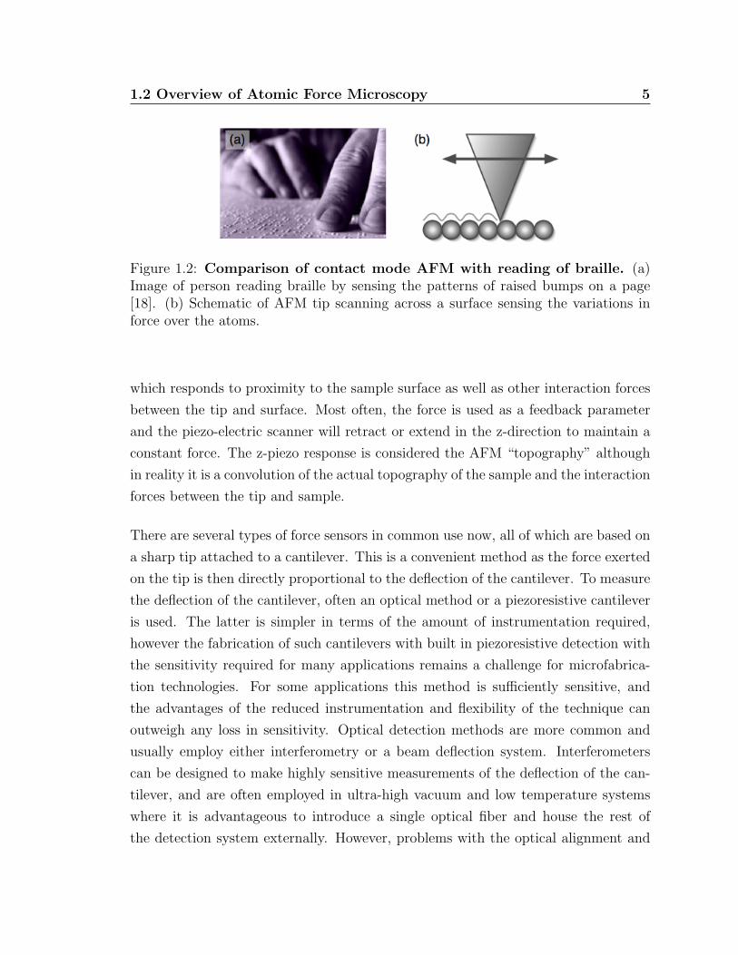
Contact-mode AFM is much like the sense of “touch” in that the shape and texture
of surfaces is determined by measuring local forces. In contact mode AFM, a sharp
tip is raster scanned over a surface, usually using a piezo-electric scanner, much as a
blind person moves their hands across a page to sense the patterns of raised bumps
which constitute words in braille (see fig. 1.2). The tip is attached to a force sensor
1.2 Overview of Atomic Force Microscopy 5
Figure 1.2: Comparison of contact mode AFM with reading of braille. (a)Image of person reading braille by sensing the patterns of raised bumps on a page[18]. (b) Schematic of AFM tip scanning across a surface sensing the variations inforce over the atoms.
which responds to proximity to the sample surface as well as other interaction forces
between the tip and surface. Most often, the force is used as a feedback parameter
and the piezo-electric scanner will retract or extend in the z-direction to maintain a
constant force. The z-piezo response is considered the AFM “topography” although
in reality it is a convolution of the actual topography of the sample and the interaction
forces between the tip and sample.
There are several types of force sensors in common use now, all of which are based on
a sharp tip attached to a cantilever. This is a convenient method as the force exerted
on the tip is then directly proportional to the deflection of the cantilever. To measure
the deflection of the cantilever, often an optical method or a piezoresistive cantilever
is used. The latter is simpler in terms of the amount of instrumentation required,
however the fabrication of such cantilevers with built in piezoresistive detection with
the sensitivity required for many applications remains a challenge for microfabrica-
tion technologies. For some applications this method is sufficiently sensitive, and
the advantages of the reduced instrumentation and flexibility of the technique can
outweigh any loss in sensitivity. Optical detection methods are more common and
usually employ either interferometry or a beam deflection system. Interferometers
can be designed to make highly sensitive measurements of the deflection of the can-
tilever, and are often employed in ultra-high vacuum and low temperature systems
where it is advantageous to introduce a single optical fiber and house the rest of
the detection system externally. However, problems with the optical alignment and
6 Chapter 1. Introduction and Background
approach of the fiber over the small cantilever can be inconvenient. Beam deflection
systems operate by focusing a laser on the back of a cantilever where it is reflected
into a split or quadrant photodiode. As the cantilever bends, the position of the re-
flected beam on the photodiode will change, and thus give a measure of the deflection
of the cantilever. Beam deflection systems require more “onboard” instrumentation,
ie, a laser, a photodetector, and some scheme of aligning both, and are thus more
commonly found in ambient and liquid AFM systems, though many vacuum systems
also now employ this technique.
A major advantage of a beam deflection system over an interferometer for measuring
the deflection of the AFM cantilever is the ability to measure lateral forces as well as
normal forces when a quadrant photodiode is used. Lateral-force AFM (LF-AFM),
or friction force microscopy (FFM), is of great interest in the field of nano-tribology,
or the study of friction on the nano-scale. Of recent interest is the study of atomic
stick-slip motion under ultra-high vacuum conditions [19, 20] in the hopes that it will
advance our understanding of friction mechanisms on the atomic scale. Manipula-
tion experiments have been of significant interest as a method of building prototype
molecular devices, and the information obtained from LF-AFM could greatly improve
understanding of the underlying mechanisms involved in these processes. It has been
proposed that frictional effects between an adsorbate (a single asperity contact) and
an atomically flat surface may play a role in single molecule manipulation experi-
ments [21]. Also, a variation of LF-AFM was recently used to measure forces exerted
on and by the tip during a single molecule manipulation [22].
Applications of contact and intermittent contact, or “tapping” mode, AFM appear in
a growing number of fields. AFM is now frequently used in the imaging and probing of
mechanical and electrical properties of biological system ranging from large cells down
to single bio-molecules. It is also used in chemistry and engineering to characterize
the quality of thin films and the roughness of surfaces.
1.2 Overview of Atomic Force Microscopy 7
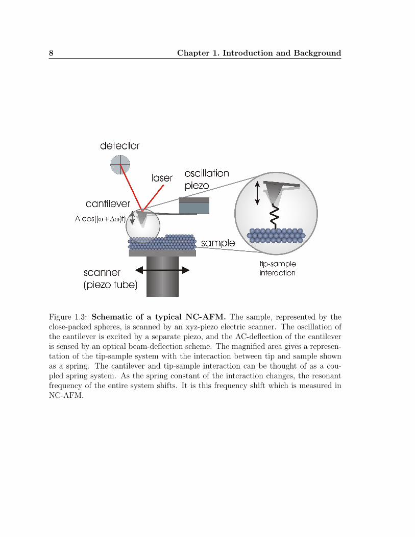
1.2.2 Non-contact atomic force microscopy
Unlike the previous section where a static mode of imaging is described, an oscillating
cantilever may be used in a dynamic imaging mode. As in contact mode imaging,
a sharp tip is raster scanned over the surface and the recorded signals provide feed-
back and mapping of the specimen of interest. There are two such methods of force
detection for AFM, relying on amplitude modulation (AM) or frequency modulation
(FM) detection. The first, more common, is often referred to as ”tapping” or inter-
mittent contact mode. In this mode the cantilever is excited at a fixed amplitude and
oscillation frequency at or near the resonant frequency of the cantilever. A reduction
in the amplitude indicates an often repulsive interaction between the tip and sample
and is used as a feedback parameter. Alternatively, a frequency detection mode can
be used where the cantilever is similarly excited at or near its resonant frequency,
but the change in frequency of the cantilever and tip–sample interaction system is
measured (see fig. 1.3). The excitation is altered to track the resonance of this com-
bined system. Additionally, the tip is generally maintained at a distance such that it
remains in the attractive regime of the tip–sample interaction, hence the term “non-
contact”. Since NC-AFM remains in this attractive regime it is less destructive than
tapping mode. However, because the cantilevers must have high Q-factors, NC-AFM
is usually performed in a vacuum or low temperature environment making it unsuit-
able for most biological applications. This frequency modulation AFM (FM-AFM)
has also been coined dynamic scanning force microscopy (DSFM), or most commonly
non-contact AFM (NC-AFM).
In NC-AFM mode, the sharp tip is oscillated over the surface and as the interaction
between the tip and sample changes, the resonant frequency of the cantilever and tip-
sample interaction system changes. This is analogous to a coupled spring system in
which the spring constant of one of the components is variable, altering the resonance
frequency of the system (see fig. 1.3). In this way, the frequency shift of the system
is a measure of the tip-sample interaction. This frequency shift is proportional to
the force gradient in the small amplitude limit, where the amplitude of oscillation is
small compared to the tip-sample separation. For large amplitude oscillations, the
frequency shift is related to the interaction in a more complex way [23]:
8 Chapter 1. Introduction and Background
Figure 1.3: Schematic of a typical NC-AFM. The sample, represented by theclose-packed spheres, is scanned by an xyz-piezo electric scanner. The oscillation ofthe cantilever is excited by a separate piezo, and the AC-deflection of the cantileveris sensed by an optical beam-deflection scheme. The magnified area gives a represen-tation of the tip-sample system with the interaction between tip and sample shownas a spring. The cantilever and tip-sample interaction can be thought of as a cou-pled spring system. As the spring constant of the interaction changes, the resonantfrequency of the entire system shifts. It is this frequency shift which is measured inNC-AFM.
1.2 Overview of Atomic Force Microscopy 9
∆f
f0
kA =
∫ 2π
0
dφ
2πF (z + A cos(φ)) cos(φ) (1.1)
where ∆f is the frequency shift, f0 is the resonant frequency of the cantilever, k is
the spring constant of the cantilever, A is the amplitude of the oscillations, and the
variable of integration, φ, is the angular position of the cantilever at any given time, ie.
the force is integrated over one full cycle of the cantilever oscillation. There are several
methods which have been developed to convert frequency shift to force [24, 25] which
will not be discussed here, though it is necessary for detailed quantitative analysis of
many results.
As in contact mode AFM, NC-AFM is sensitive to a combination of forces. The three
main contributions are electrostatic (long-range), van der Waals (long/intermediate-
range), and chemical (short range). The electrostatic contribution to the frequency
shift can be expressed as [23]:
∆felec
f0
kA = −πε0R(Vbias − VCPD)2
√2sA
(1.2)
where ∆felec is the electrostatic contribution to the frequency shift, f0 is the resonant
frequency of the cantilever, k is the spring constant of the cantilever, A is the ampli-
tude of oscillation, R is the radius of the tip, Vbias is an applied bias between the tip
and sample, VCPD is the contact potential difference, and s is the distance between
the sample and the macroscopic portion of the tip. The contact potential difference
is a property of both the tip and sample materials and is related to the difference in
work function of those two materials, and is defined as [26]:
VCPD =1
e(Φtip − Φsample) (1.3)
where Φtip is the work function of the tip material, and Φsample is the work function
of the sample material.
10 Chapter 1. Introduction and Background
Note that by applying a bias voltage, the electrostatic contribution to the frequency
shift can be minimized. This is often advantageous as long range electrostatic forces
can make small features difficult or impossible to resolve as the forces measured are
not local on the atomic scale [27]. Also note that there is a s−1/2 dependance of the
frequency shift on distance between the macroscopic tip and the sample indicating
that the effect is long range, as well as a quadratic relationship between frequency
shift and bias voltage.
Similarly, the van der Waals contribution to the frequency shift can be expressed as
[23]:
∆fvdW
f0
kA = − HR
12s√
2sA(1.4)
where ∆fvdW is the van der Waals contribution to the frequency shift, H is the
Hamaker constant and can be taken as the geometric mean of the Hamaker constants
for the tip and sample. Note that there is a s−3/2 dependance of the frequency shift
on the distance between the macroscopic tip and the sample due to the van der Waals
contribution.
Taking the chemical interaction to be well modeled by the Morse potential, and
assuming that the tip does not enter the repulsive regime of the chemical potential,
an expression for the chemical contribution to the frequency shift can be derived from
the attractive portion of the Morse potential [23]:
∆fchem
f0
kA = − U0√πAλ
√2e
−s−s0λ (1.5)
where ∆fchem is the chemical contribution to the frequency shift, U0 is the depth of the
chemical potential, λ is the characteristic interaction length, s0 is the position of the
minimum of the chemical potential, and s is the distance between the microscopic
apex of the tip and the sample. Here there is a much stronger, ie. exponential,
dependence on the tip-sample separation, but only at short range. For high resolution
1.2 Overview of Atomic Force Microscopy 11
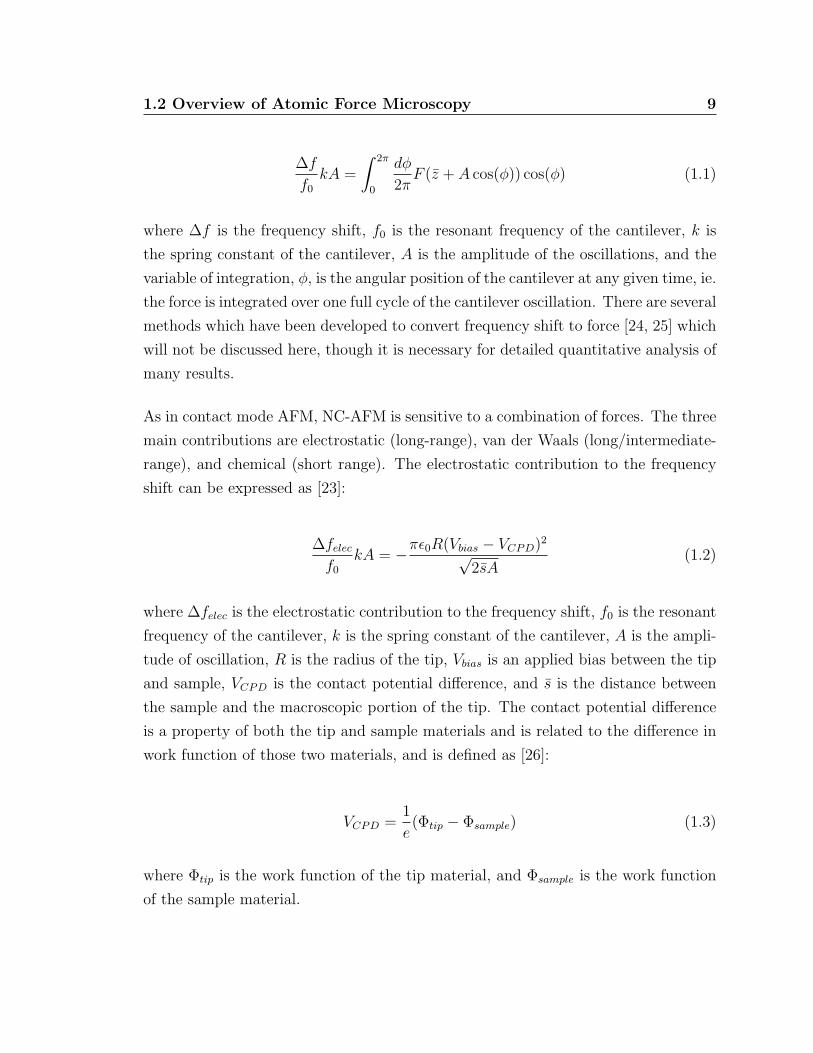
Figure 1.4: Example of frequency shift vs. distance relation showing con-trast inversion The images in (a) and (b) show the Au(111) herringbone reconstruc-tion in both normal (∆f = −85Hz, A=6nm) and inverted (∆f = −98Hz, A=6nm)contrast respectively (images from [28]). The solid curve in (c) represents a typical∆f vs. distance relation according to the sum of the electrostatic, van der Waals, andMorse potential contributions to ∆f . The dashed line is shifted in z a small amountrepresenting a topographical height difference between two regions of the sample, andhas a different CPD from the first. The cross-over between the two curves separatesthe regions of normal and inverted contrast. The arrows along the bottom axis ofthe graph point towards the solid curve, the direction indicating whether this regionappears topographically higher (arrow pointing to the right) or lower (arrow pointingto the left).
imaging of many materials it is necessary to be in the regime where the chemical
interaction dominates.
Due to the different contributing interactions, and the different length scales over
which they dominate, it is possible to have an apparent inverted contrast over inho-
12 Chapter 1. Introduction and Background
mogeneous regions of a sample depending on the relative strengths of the contribu-
tions to the frequency shift. For example see figure 1.4 where for two different regions,
represented by different frequency shift vs. distance curves, the frequency shift vs.
distance relations can have cross-over points resulting in an inversion of contrast in
the image [29, 28].
NC-AFM has developed into a number of different tools for different applications
including magnetic force microscopy (MFM), electrostatic force microscopy (EFM),
and Kelvin probe microscopy (KPM). These different modes of imaging allow inves-
tigation of many different types of samples, giving NC-AFM additional functionality
beyond its high resolution capabilities.
1.3 Brief theory of Growth and Epitaxy
Both the growth of deposited materials and the final structure of the overlayer depend
on a delicate balance of energetics and kinetics. An understanding of the growth of
a given material on a specific substrate, as well as a determination of the final struc-
ture, can provide information about the interactions between the deposited atoms
or molecules and the deposit–substrate interactions. The field of scanning probe mi-
croscopy has opened a window into the microscopic world of growth allowing study
of nucleation and the early stages of growth [12].
1.3.1 Nucleation and growth concepts
Nucleation and growth processes are governed by a combination of equilibrium ther-
modynamic processes and non-equilibrium kinetic processes. These occur both on an
atomic scale, where nucleation takes place, and on the large scale where the island
or layer morphology forms during continuing growth.
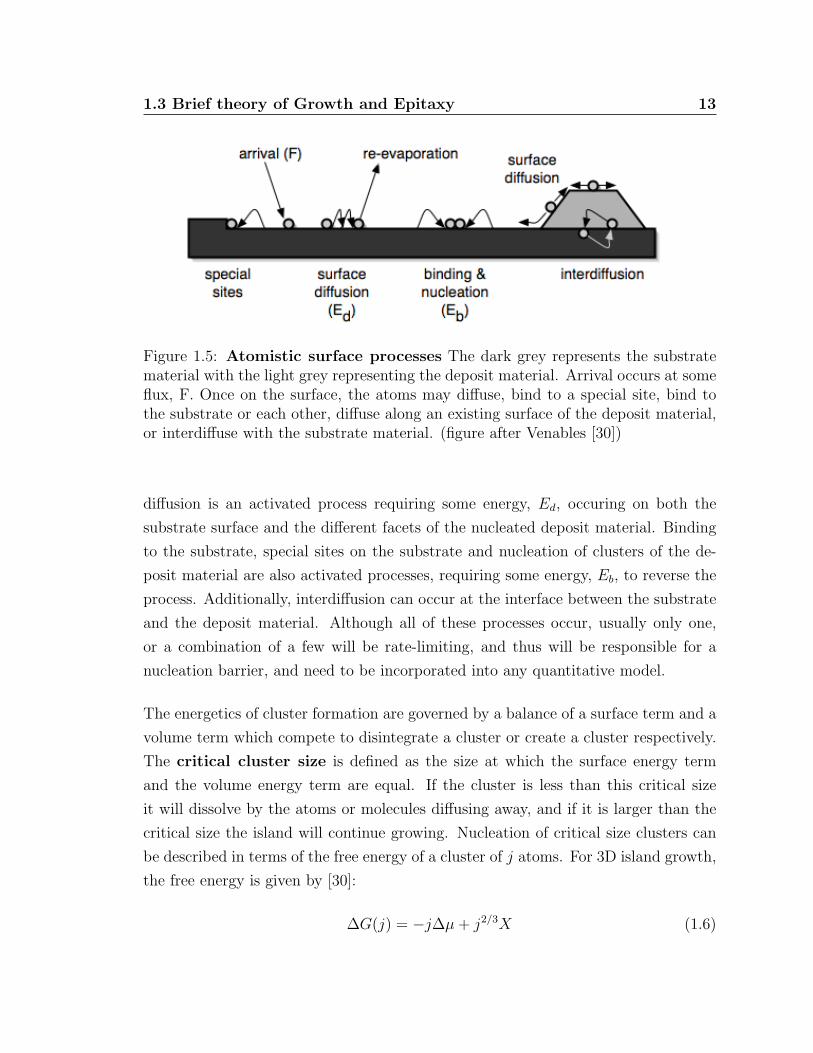
Atomistic processes during adsorption include arrival of the atoms at a flux F , re-
evaporation, surface diffusion and binding and nucleation (see fig. 1.5). Surface
1.3 Brief theory of Growth and Epitaxy 13
Figure 1.5: Atomistic surface processes The dark grey represents the substratematerial with the light grey representing the deposit material. Arrival occurs at someflux, F. Once on the surface, the atoms may diffuse, bind to a special site, bind tothe substrate or each other, diffuse along an existing surface of the deposit material,or interdiffuse with the substrate material. (figure after Venables [30])
diffusion is an activated process requiring some energy, Ed, occuring on both the
substrate surface and the different facets of the nucleated deposit material. Binding
to the substrate, special sites on the substrate and nucleation of clusters of the de-
posit material are also activated processes, requiring some energy, Eb, to reverse the
process. Additionally, interdiffusion can occur at the interface between the substrate
and the deposit material. Although all of these processes occur, usually only one,
or a combination of a few will be rate-limiting, and thus will be responsible for a
nucleation barrier, and need to be incorporated into any quantitative model.
The energetics of cluster formation are governed by a balance of a surface term and a
volume term which compete to disintegrate a cluster or create a cluster respectively.
The critical cluster size is defined as the size at which the surface energy term
and the volume energy term are equal. If the cluster is less than this critical size
it will dissolve by the atoms or molecules diffusing away, and if it is larger than the
critical size the island will continue growing. Nucleation of critical size clusters can
be described in terms of the free energy of a cluster of j atoms. For 3D island growth,
the free energy is given by [30]:
∆G(j) = −j∆µ + j2/3X (1.6)
14 Chapter 1. Introduction and Background
where ∆G(j) is the free energy of a cluster of j atoms, ∆µ is the chemical potential,
or in this case the supersaturation, and X is the surface energy term. The surface
energy can be expressed as a sum of the surface energy of the deposit material island
and the interface energy [30]:
X =∑
k
Ckγk + CAB(γ∗ − γB) (1.7)
where the first term is a sum over the surface energies of all facets of the deposited
island, and the second term corresponds to the interface energy. The maximum in
the free energy (eqn. 1.6) corresponds to a nucleation barrier, and thus the cluster
size corresponding to this maximum is the smallest possible stable cluster. Below
this critical cluster size, the atoms will dissociate and diffuse away to reform clusters
until a sufficient number of stable clusters exist to nucleate further growth. By
differentiating the free energy, one can find the critical cluster size, jcrit [30]:
∂
∂j∆G(j) = −∆µ +
2
3j−1/3X (1.8)
jcrit =( 2X
3∆µ
)3
(1.9)
The same process can be used to find the critical cluster size for 2D, or layer growth.
In this case, the starting expression for the free energy is slightly different [30]:
∆G(j) = −j∆µ′ + j1/2X (1.10)
where ∆µ′ is now related to both the chemical potential, or degree of supersaturation,
and the surface energies [30]:
1.3 Brief theory of Growth and Epitaxy 15
∆µ′ = ∆µ−∆µc (1.11)
∆µc = (γA + γ∗ − γB)Ω2/3 (1.12)
where γA is the surface energy of the deposit material, γB is the surface energy of the
substrate, γ∗ is the interface energy, and Ω is the volume of the deposit. As a side
note, ∆µ′ can also be expressed in terms of the adsorption isotherm: ∆µ′ = kT ln( pp0
),
such that the step height of the adsorption isotherm corresponds to the difference in
surface energy in eqn. 1.12. That aside, differentiation of the free energy (eqn. 1.10)
leads to a critical 2D cluster size given by [30]:
jcrit =( X
2∆µ′
)2
(1.13)
This thermodynamic description of nucleation is somewhat oversimplified as it leaves
out some of the kinetic process which can effect nucleation, and applies macroscopic
quantities on a microscopic system, especially since critical clusters can often be
as small as one atom. As such, there are many atomistic models that deal with
nucleation and subsequent growth which will not be discussed here.
It is worth noting at this point however, that the critical cluster size, as well as
parameters related to the diffusion of the deposited material can be found experi-
mentally through the expressions derived from mean-field nucleation theory for the
density of islands. Starting from the rate equations describing the density of stable
2D islands and monomers with no re-evaporation, it can be shown that in the limit
of saturation, the density of large stable clusters, nx is given by [12]:
nx = η(θ, j)(D
F
)−χ
exp( Ej
(i + 2)kT
)(1.14)
where D is the diffusion rate, η is an exponential pre-factor dependent on coverage, θ,

16 Chapter 1. Introduction and Background
and cluster size, j. Ej is the binding energies of a cluster of size jcrit, and the exponent
χ can be expressed in terms of the critical cluster size: χ = jcrit/(jcrit + 2). In the
saturation limit, the ratio D/F can also be expressed in terms of a characteristic
length, l, which is the mean island distance and also the mean free path of diffusing
adatoms [12]:
D
F' l6
ln(l2)' l6 (1.15)
In this way, the ratio D/F can be found experimentally and a plot of log(D/F )
vs. log(nx) can be used to determine the exponent χ and subsequently the critical
island size. Additionally, under conditions where dimers are stable, ie. jcrit = 1, an
Arrhenius plot can be used to extract the migration barrier and attempt frequency
for diffusion of the adsorbate.
The time evolution of submonolayer growth proceeds from nucleation, where a su-
persaturated background is required, through diffusive growth, where the super-
saturated background is depleted by the growing nuclei, to a coarsening stage at
low supersaturation, where growth of some islands is at the expense of others which
dissolve into the background. As the first nuclei begin to form they gather material
from the surrounding area, and thus begin to deplete the initially uniform supersat-
urated background. The nucleation rate, and the distribution of the nucleation rate,
will depend on the conditions of the growth, such as the supersaturation, the tem-
perature, and other conditions which may effect the initial dispersion of the nuclei
(eg. surface defects). As the initial nuclei continue to grow in the diffusive regime,
the density of islands remains roughly constant, and the islands are similar in size.
The supersaturated background provides the islands with material to continue grow-
ing at roughly the same rate continuing to give a narrow size distribution. Before
growth can proceed into coarsening, or Ostwald ripening, the supersaturation must
be depleted to a point where small islands begin to break apart and that material is
available to diffuse through the supersaturated background to continue growth [31].
In the case where there is a constant flux of material deposited, this last stage does
not necessarily occur without a further annealing process [12].
1.3 Brief theory of Growth and Epitaxy 17
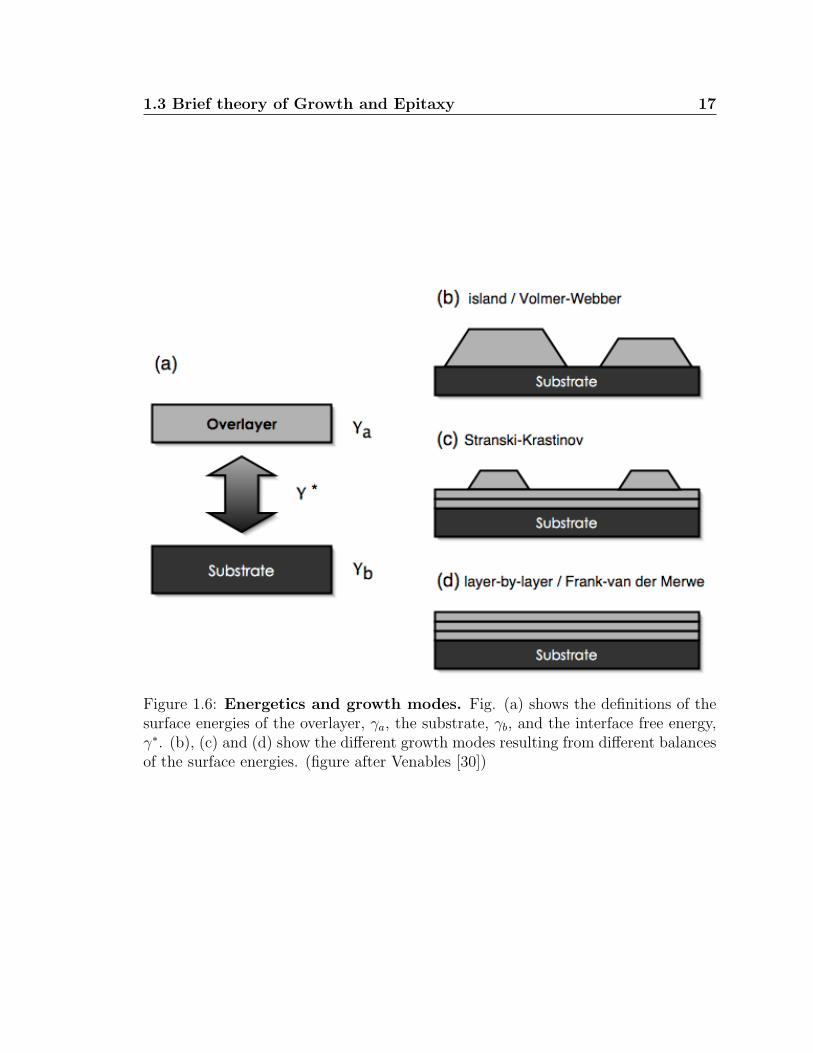
Figure 1.6: Energetics and growth modes. Fig. (a) shows the definitions of thesurface energies of the overlayer, γa, the substrate, γb, and the interface free energy,γ∗. (b), (c) and (d) show the different growth modes resulting from different balancesof the surface energies. (figure after Venables [30])
18 Chapter 1. Introduction and Background
From a more macroscopic view, the balance of the surface energies of the substrate
and deposit material, as well as the interface energy (see fig. 1.6) dictate the way the
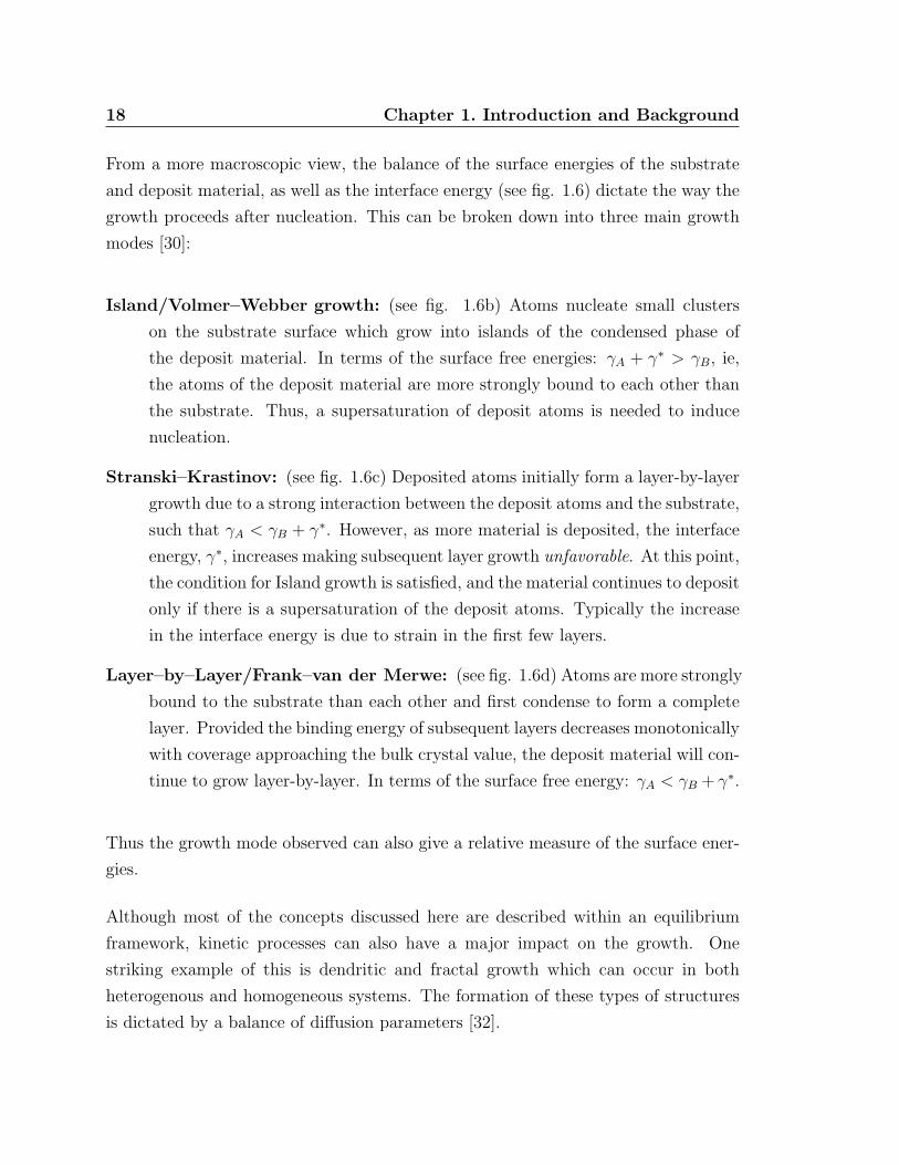
growth proceeds after nucleation. This can be broken down into three main growth
modes [30]:
Island/Volmer–Webber growth: (see fig. 1.6b) Atoms nucleate small clusters
on the substrate surface which grow into islands of the condensed phase of
the deposit material. In terms of the surface free energies: γA + γ∗ > γB, ie,
the atoms of the deposit material are more strongly bound to each other than
the substrate. Thus, a supersaturation of deposit atoms is needed to induce
nucleation.
Stranski–Krastinov: (see fig. 1.6c) Deposited atoms initially form a layer-by-layer
growth due to a strong interaction between the deposit atoms and the substrate,
such that γA < γB + γ∗. However, as more material is deposited, the interface
energy, γ∗, increases making subsequent layer growth unfavorable. At this point,
the condition for Island growth is satisfied, and the material continues to deposit
only if there is a supersaturation of the deposit atoms. Typically the increase
in the interface energy is due to strain in the first few layers.
Layer–by–Layer/Frank–van der Merwe: (see fig. 1.6d) Atoms are more strongly
bound to the substrate than each other and first condense to form a complete
layer. Provided the binding energy of subsequent layers decreases monotonically
with coverage approaching the bulk crystal value, the deposit material will con-
tinue to grow layer-by-layer. In terms of the surface free energy: γA < γB + γ∗.
Thus the growth mode observed can also give a relative measure of the surface ener-
gies.
Although most of the concepts discussed here are described within an equilibrium
framework, kinetic processes can also have a major impact on the growth. One
striking example of this is dendritic and fractal growth which can occur in both
heterogenous and homogeneous systems. The formation of these types of structures
is dictated by a balance of diffusion parameters [32].

1.3 Brief theory of Growth and Epitaxy 19
1.3.2 Epitaxy of organic molecules
Standard discussions of epitaxy generally refer to simple atomic systems where the
deposited material is similar to the substrate material in size, symmetry, and interac-
tion strength and stiffness. Where the symmetry and the size of the overlayer lattice
is similar to the substrate, the degree of epitaxy is usually given in terms of the 1D
lattice mismatch parameter:
f =(b− a)
a(1.16)
where b is the overlayer lattice constant, and a is the substrate lattice constant.
However, this 1D parameter is only meaningful for lattices with the same symmetry.
For molecular overlayers, this is often not the case as many molecular films have a
low symmetry and large lattice constants compared to most substrates.
Additionally, the structural arrangement of organic molecules on surfaces is deter-
mined by a complex interplay of molecule–molecule interactions, substrate–overlayer
interactions, and lattice geometries. The “soft” (often Van der Waals in origin) in-
teractions between molecules gives the overlayer a relatively small elastic constant
as compared to typical inorganic materials, allowing the overlayer lattice to deform
in order to accomodate the substrate. Similarly, the interactions with the substrate
may be weak (especially in the case of insulators which are examined here), and
also “soft”. This often leads to structures which are not commensurate (molecule A,
sticks to specific site on substrate B), but coincident where there is a distinct lattice
registry, but the substrate–overlayer interaction is not necessarily minimized. As it
is this balance of competing interactions which dictate the structure of the overlayer,
determination of the structural relationship between the overlayer and substrate can
also reveal information about the relative strengths and stiffnesses of the interactions
in the system without knowledge of the detailed forms of the interaction potentials.
The relationship between any two lattices can be given as the matrix which transforms
the set of substrate lattice vectors into the set of overlayer vectors as given by:
20 Chapter 1. Introduction and Background
[b1
b2
]= [C]
[a1
a2
]=
[p q
r s
] [a1
a2
](1.17)
Where the symmetry of the two lattices is the same, a short-hand version of this ma-
trix is often used. Wood’s notation takes the multiplying factor required to transform
the each of the substrate lattice vectors to each of the supercell lattice vectors, and
follows this with a rotation angle if required. For example, the matrix:
[2 2
2 2
](1.18)
would be written as√
2 ×√
2R45, since each of the supercell lattice vectors is√
2
times longer than the substrate lattice vectors, and the supercell lattice is rotated by
an angle of 45 from the substrate lattice. This particular cell can also be written as
c2× 2, where a supercell that has the same orientation as the substrate lattice, and
edges that are two times the length of the substrate lattice vectors, but has one extra
overlayer atom in the center of the cell. Wood’s notation is a very convenient way of
stating an overlayer structure, however, since there is no way of defining a different
angle between the overlayer lattice vectors from the substrate lattice vectors, it can
only be applied to systems which have the same basic symmetry. Since molecular
systems often have a different symmetry from the substrates they are deposited on,
matrix notation must be used to define an epitaxial relation.
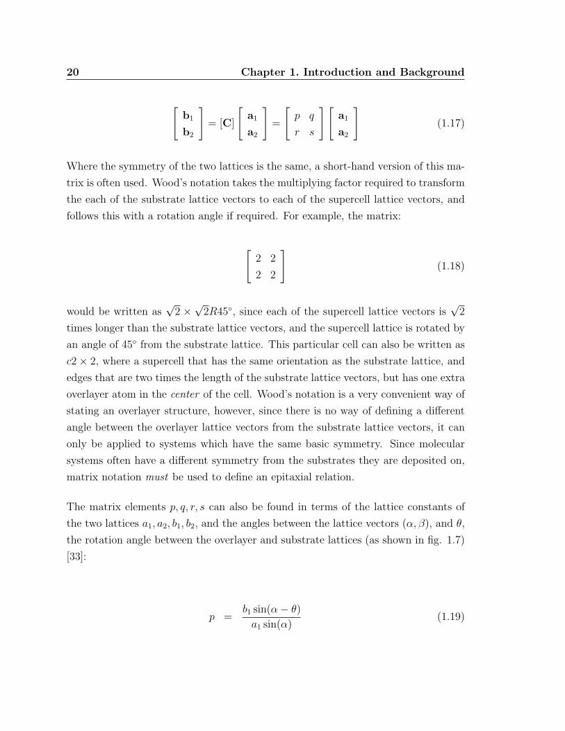
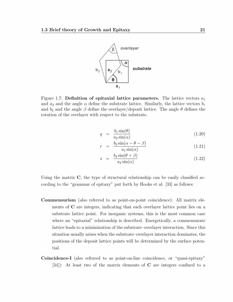
The matrix elements p, q, r, s can also be found in terms of the lattice constants of
the two lattices a1, a2, b1, b2, and the angles between the lattice vectors (α, β), and θ,
the rotation angle between the overlayer and substrate lattices (as shown in fig. 1.7)
[33]:
p =b1 sin(α− θ)
a1 sin(α)(1.19)
1.3 Brief theory of Growth and Epitaxy 21
Figure 1.7: Definition of epitaxial lattice parameters. The lattice vectors a1
and a2 and the angle α define the substrate lattice. Similarly, the lattice vectors b1
and b2 and the angle β define the overlayer/deposit lattice. The angle θ defines therotation of the overlayer with respect to the substrate.
q =b1 sin(θ)
a2 sin(α)(1.20)
r =b2 sin(α− θ − β)
a1 sin(α)(1.21)
s =b2 sin(θ + β)
a2 sin(α)(1.22)
Using the matrix C, the type of structural relationship can be easily classified ac-
cording to the “grammar of epitaxy” put forth by Hooks et al. [33] as follows:
Commensurism (also referred to as point-on-point coincidence): All matrix ele-
ments of C are integers, indicating that each overlayer lattice point lies on a
substrate lattice point. For inorganic systems, this is the most common case
where an “epitaxial” relationship is described. Energetically, a commensurate
lattice leads to a minimization of the substrate–overlayer interaction. Since this
situation usually arises when the substrate–overlayer interaction dominates, the
positions of the deposit lattice points will be determined by the surface poten-
tial.
Coincidence-I (also referred to as point-on-line coincidence, or “quasi-epitaxy”
[34]): At least two of the matrix elements of C are integers confined to a
22 Chapter 1. Introduction and Background
single column of the matrix. This defines the situation where every overlayer
lattice point lies on at least one primitive lattice line of the substrate, hence
the alternate terminology of “point-on-line (POL)” coincidence. Coincidence-I
can be subdivided into two catagories:
Coincidence-IA : All matrix elements are rational numbers. In this case
a supercell can be constructed, defining a phase coherent registry with
the lattice, even though some overlayer lattice points do not lie on lattice
points of the substrate. In inorganic systems this is typically referred to
simply as “coincidence”. In terms of the substrate–overlayer interaction,
the situation of coincidence-IA is energetically less favorable than com-
mensurism as some of the overlayer lattice points will be out of phase with
the substrate lattice, even though a longer range phase coherence still ex-
ists. Of course, when the full set of interactions is considered, this may
still be an energetic minimum for the system.
Coincidence-IB : At least one of the matrix elements of C is an irrational
number. Although every overlayer lattice point lies on one primitive lattice
line of the substrate, the irrational matrix element produces an incommen-
surate relationship in one direction. Due to this incommensurate relation
in one direction, a finite supercell cannot be constructed. (Note: If the
supercell size exceeds the area investigated experimentally, coincidence-IA
will be indistinguishable from coincidence-IB.)
Coincidence-II (also called “geometrical coincidence”): All matrix elements are
rational, but no column consists of integers. In this case a supercell can still be
constructed, but not all of the lattice points of the overlayer lie on at least one
substrate lattice line. Although this case violates the reciprocal space criterion
(b∗1 = ma∗1, where m is an integer), it is still considered coincidence due to the
presence of a lattice registry (supercell can be constructed). Again, coincidence-
II is less energetically favorable in terms of the overlayer–substrate interaction
than the aforementioned cases.
Incommensurism : The matrix C has at least one irrational element and neither
column consists of integers. In this case there is no finite size supercell which can
1.4 C60 on KBr: prototypical system 23
be constructed, and hence no distinct lattice registry between the overlayer and
the substrate. Incommensurism is the least favorable in terms of the interface
energy and will occur in the absence of an available phase-coherent structure.
The type of geometrical arrangement as described above that is actually present in a
given system will depend upon the relative strengths and elasticities of the overlayer–
substrate interaction and the intralayer interaction, as well as the availability of
a lattice matching geometry. In many cases for molecular systems, the relatively
soft intralayer and overlayer–substrate interactions (ie. small elastic constants, or
potential wells with low curvature) lead to coincident structures that are indeed
energetically favorable.
1.4 C60 on KBr: prototypical system
KBr is an ionic salt (alkali halide) with a cubic NaCl structure (fcc with a basis).
The conventional unit cell has a lattice constant of 6.60 A, which is maintained at
the surface with insignificant rumpling [35] (see fig. 1.8). KBr is easily cleaved along
the 100 planes. It is relatively inert, and is primarily sensitive to water and CO
contamination at step edges. KBr is considered an insulator, and has a dielectric
constant of 5.65 at 25C over a frequency range of 100–1×10⁹Hz [36].
C60 , the third elemental form of carbon (after graphite and diamond in abundance
respectively), was disovered by Kroto and Smalley in 1985 [37]. Sixty carbon atoms
form a spherical cage with each of the atoms located at the vertices of a truncated
icosahedron, or the shape of a soccer ball (see fig. 1.8). The C60 molecule owes
its nickname “buckyball” to its resemblance to the geodesic domes designed by R.
Buckminster Fuller. The van der Waals radius of a single C60 molecule is ∼ 7 A[37],
and in bulk, C60 forms an fcc crystal with an intermolecular spacing of 10.2 A[38].
Previous results from STM have shown that the binding energy of C60 depends a great
deal on the substrate, interacting strongly with metal and semiconducting surfaces,
and much more weakly with oxide (insulating) surfaces [38].
24 Chapter 1. Introduction and Background
Both KBr and C60 are well studied systems within the NC-AFM and STM commu-
nities respectively. Atomic resolution was achieved on an alkali halide in 1997 by
Bammerlin et. al. [39] and the sample preparation of these substrates is well docu-
mented. The ability to achieve atomic resolution on the substrate is important both
for understanding the growth of the molecular species on the surface as well as for
future molecular electronics experiments where the substrate may influence the elec-
trical properties of the molecule. C60 was chosen both for its potential application in
molecular electronics [40, 41], as well as its simple geometry. The spherical geometry
of C60 makes ab initio computations involving the molecule more tractable. Such
calculations may be used in understanding the interaction between the molecule and
the substrate in understanding growth, as well as modeling electrical properties to
compare to the measurement of a future molecular device. Additionally, the relatively
large size, and spherical shape of the C60 molecule makes it potentially easier to image
as it is expected to have a larger corrugation, when considering geometry alone, than
a large flat molecule such as a porphyrin, metal-pthalocyanine, or perylene derivative.
Although literature on growth of molecules on insulating surface is scarce, there have
been some studies of C60 on various insulators, including alkali halides [9, 42, 43].
These studies were performed with a variety of techniques including contact mode
AFM (and lateral force AFM) and electron microscopy. However, as discussed pre-
viously, these techniques often do not provide high resolution information, or are
destructive to the sample surface being investigated. NC-AFM offers the possibility
of both non-destructive and high spatial resolution investigation of both films and
nanostructures of these molecular systems on insulators. The simplicity of the C60 on
KBr(001) system and wide range of existing literature on each of the selected sub-
strate and the selected molecule make this a reasonable candidate for a prototypical
molecule-insulator system to which the NC-AFM technique can be applied to the
study of molecular nucleation and growth on an insulator.
1.4 C60 on KBr: prototypical system 25
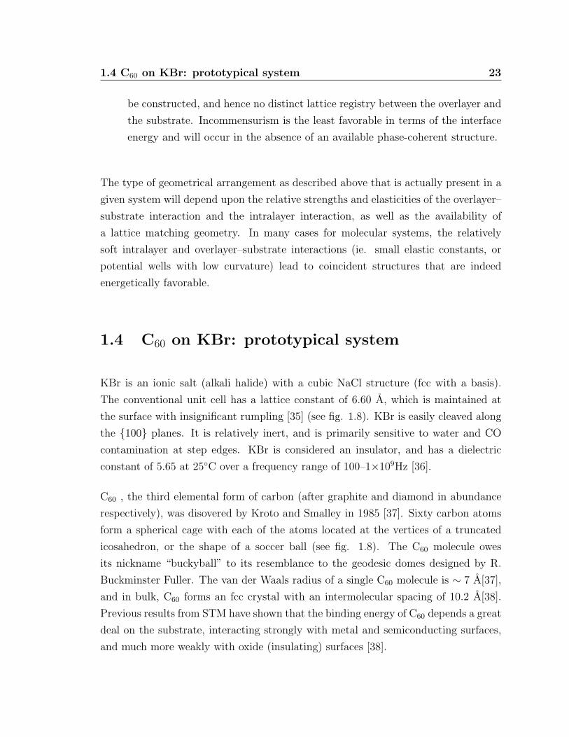
Figure 1.8: Approximately to scale model of C60 molecules on a KBr surface.A KBr(001) surface is shown exposed here with the bromine ions shown as small darkgrey spheres, and the potasium ions shown as larger light grey spheres. The latticeconstant of the bulk conventional cell of this cubic NaCl structure, a1 = a2 = 6.6A,is shown on the side. The ions are represented by close-packed spheres with theratio of the radii approximately equal to that of the ionic radii of K and Br. TheC60 molecules are shown on top of the KBr(001) surface with a lattice constant of∼10A, close to the bulk close-packed spacing.
Chapter 2
Experimental Methods
The instrument used for the experiments which are described herein is based on a
commercially available variable temperature, ultra-high vacuum AFM/STM/SEM
JEOL JSPM 4500a. Additional instruments and electronics have been added to the
system. Unless otherwise specified, major components were supplied by JEOL.
2.1 The Ultra-High Vacuum system
All of the experiments discussed were performed in an ultra-high vacuum (UHV)
environment. The entire vacuum system including chambers and pumps (with the
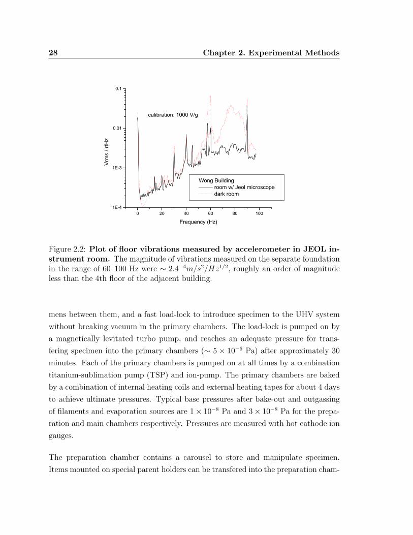
exception of a roughing pump) are mounted on an air table for vibration isolation (see
fig. 2.1). The lab floor is on a separate foundation further reducing issues of building
vibrations (see fig. 2.2). For example, a lab on the fourth floor of the adjacent
building measured vibrations with an accelerometer of 1.4 × 10⁻³m/s2/Hz1/2 for a
frequency range of 10–100Hz, which is roughly an order of magnitude larger than
measured in the JEOL instrument lab of 2.4 × 10⁻⁴m/s2/Hz1/2 for a smaller range
of frequencies frequencies, 60–100Hz, and even less for lower frequency.
The UHV system consists of two primary chambers, a transfer arm to move speci-
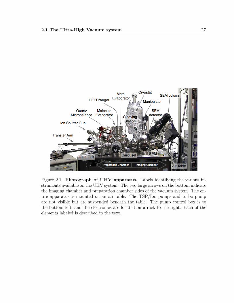
2.1 The Ultra-High Vacuum system 27
Figure 2.1: Photograph of UHV apparatus. Labels identifying the various in-struments available on the UHV system. The two large arrows on the bottom indicatethe imaging chamber and preparation chamber sides of the vacuum system. The en-tire apparatus is mounted on an air table. The TSP/Ion pumps and turbo pumpare not visible but are suspended beneath the table. The pump control box is tothe bottom left, and the electronics are located on a rack to the right. Each of theelements labeled is described in the text.
28 Chapter 2. Experimental Methods
0 20 40 60 80 1001E-4
1E-3
0.01
0.1
calibration: 1000 V/g
Vrm
s /
rtH
z
Frequency (Hz)
Wong Building room w/ Jeol microscope dark room
Figure 2.2: Plot of floor vibrations measured by accelerometer in JEOL in-strument room. The magnitude of vibrations measured on the separate foundationin the range of 60–100 Hz were ∼ 2.4−4m/s2/Hz1/2, roughly an order of magnitudeless than the 4th floor of the adjacent building.
mens between them, and a fast load-lock to introduce specimen to the UHV system
without breaking vacuum in the primary chambers. The load-lock is pumped on by
a magnetically levitated turbo pump, and reaches an adequate pressure for trans-
fering specimen into the primary chambers (∼ 5 × 10⁻⁶ Pa) after approximately 30
minutes. Each of the primary chambers is pumped on at all times by a combination
titanium-sublimation pump (TSP) and ion-pump. The primary chambers are baked
by a combination of internal heating coils and external heating tapes for about 4 days
to achieve ultimate pressures. Typical base pressures after bake-out and outgassing
of filaments and evaporation sources are 1× 10⁻⁸ Pa and 3× 10⁻⁸ Pa for the prepa-
ration and main chambers respectively. Pressures are measured with hot cathode ion
gauges.
The preparation chamber contains a carousel to store and manipulate specimen.
Items mounted on special parent holders can be transfered into the preparation cham-
2.1 The Ultra-High Vacuum system 29
ber via the load-lock transfer arm, and can likewise be transfered into the main obser-
vation chamber via a second transfer arm. The carousel can be rotated and tilted for
coarse alignment with the various preparation and characterization tools available,
and has micrometer screws for additional fine alignment.
The main observation chamber has a linear manipulator to allow specimen, ie, samples
and tips, to be transfered from the parent holders to the observation stage. The
manipulator can be moved back and forth along a track as well as up and down to
lift specimen out of the parent holders and place them on the stage. The specimen
are picked up by means of a pin which can be opened and closed by a solenoid. This
pin can only be released again when a downward force is applied as achieved when
placing a tip or sample in the tip or sample positions of the stage, or in a parent holder.
This ensures that the specimen are securely in place before the manipulator can be
disengaged. Also, to prevent excessive force from being applied to the piezo when
placing samples into the stage, there is a force meter on the side of the manipulator,
and the pin is designed to release before a damaging force would be applied.
2.1.1 Description of removable elements
There are several removable elements of the system which have some built-in func-
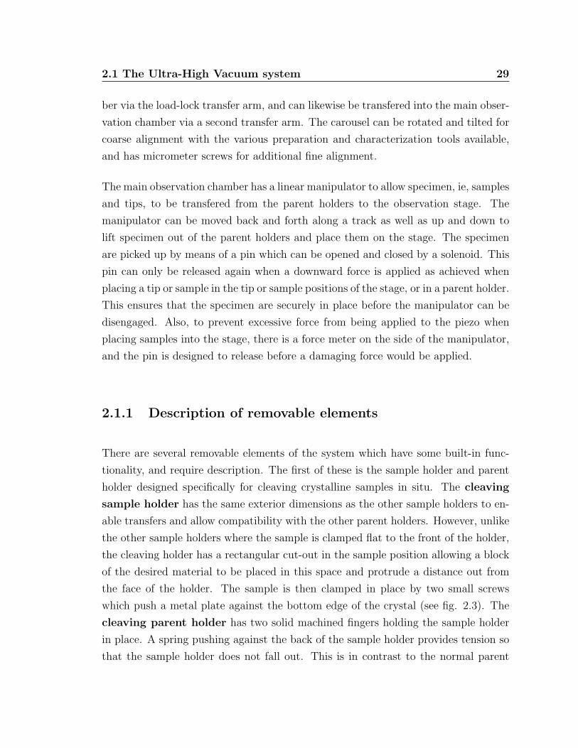
tionality, and require description. The first of these is the sample holder and parent
holder designed specifically for cleaving crystalline samples in situ. The cleaving
sample holder has the same exterior dimensions as the other sample holders to en-
able transfers and allow compatibility with the other parent holders. However, unlike
the other sample holders where the sample is clamped flat to the front of the holder,
the cleaving holder has a rectangular cut-out in the sample position allowing a block
of the desired material to be placed in this space and protrude a distance out from
the face of the holder. The sample is then clamped in place by two small screws
which push a metal plate against the bottom edge of the crystal (see fig. 2.3). The
cleaving parent holder has two solid machined fingers holding the sample holder
in place. A spring pushing against the back of the sample holder provides tension so
that the sample holder does not fall out. This is in contrast to the normal parent
30 Chapter 2. Experimental Methods
Figure 2.3: Crystal cleaving holder and cleaving station. The cleaving holder(a) shown in front and side view with crystal in place. The parent holder is shownin (b) with the sample holder in place. The cleaving station is advanced over thecleaving parent holder. Once in place, a moveable arm pushes on the protrudingcrystal, causing it to snap off.
holder which has two spring clips, electrically isolated from one another, pushing the
sample holder against a solid back. This different design is necessary as a great deal
of force is exerted on the sample, sample holder, and the arms which hold the sample
holder during the cleaving process. Other specialty sample holders are designed for
both direct current, and indirect heating of samples, as well as a specially designed
indirect heating parent holder.
The second key removable element is the cantilever holder for AFM measurements
(see fig. 2.4). The microfabricated cantilevers (described below) are held in place
against a small piezo-electric actuator by a spring clip which can be released by
pushing up the spring clip using a special platform with a protruding pin. There are
three electrical contacts to the cantilever holder, two of which are for the piezo-electric
actuator made via the two protruding pins on the bottom of the cantilever holder.
The third contact is used to apply a voltage between the tip and sample through the
spring clip which holds the cantilever chip, and is made via a contact pad on the side
of the cantilever holder.
2.1 The Ultra-High Vacuum system 31
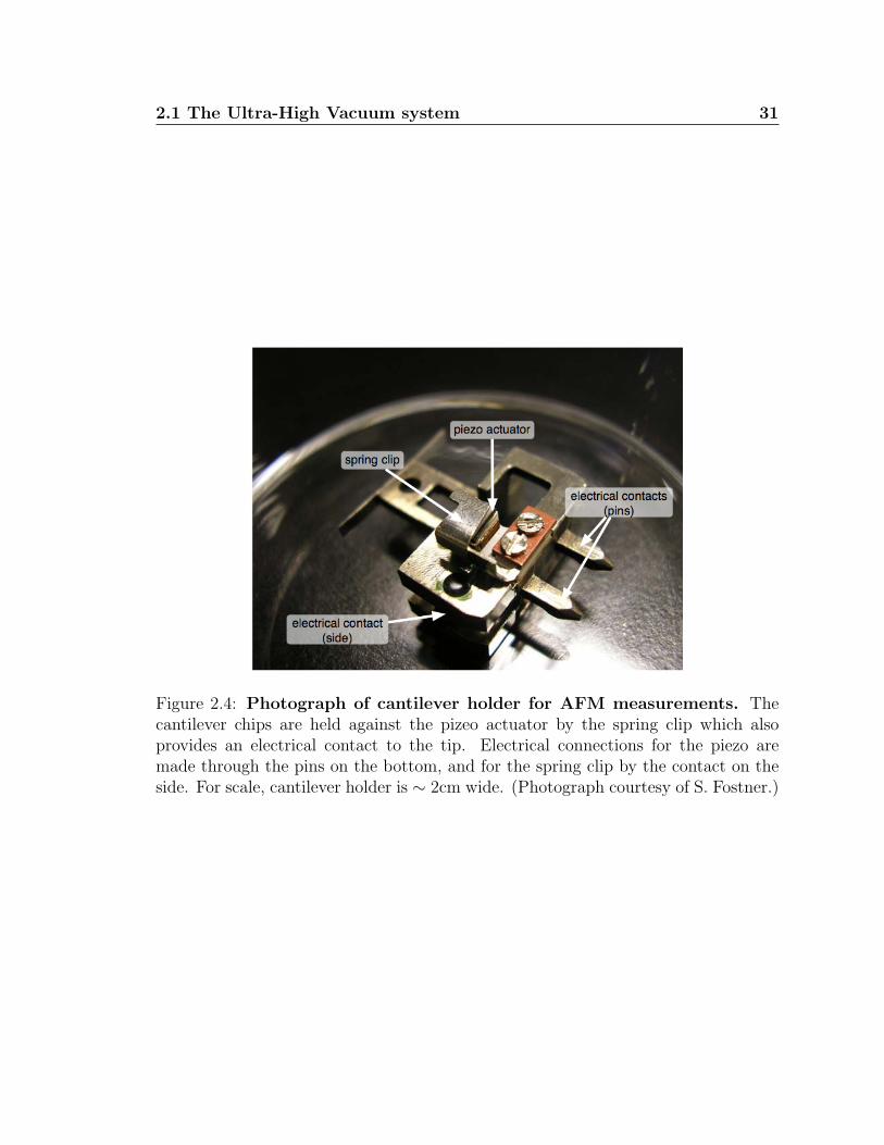
Figure 2.4: Photograph of cantilever holder for AFM measurements. Thecantilever chips are held against the pizeo actuator by the spring clip which alsoprovides an electrical contact to the tip. Electrical connections for the piezo aremade through the pins on the bottom, and for the spring clip by the contact on theside. For scale, cantilever holder is ∼ 2cm wide. (Photograph courtesy of S. Fostner.)
32 Chapter 2. Experimental Methods
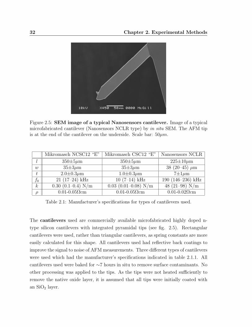
Figure 2.5: SEM image of a typical Nanosensors cantilever. Image of a typicalmicrofabricated cantilever (Nanosensors NCLR type) by in situ SEM. The AFM tipis at the end of the cantilever on the underside. Scale bar: 50µm.
Mikromasch NCSC12 “E” Mikromasch CSC12 “E” Nanosensors NCLR
l 350±5µm 350±5µm 225±10µmw 35±3µm 35±3µm 38 (20–45) µmt 2.0±0.3µm 1.0±0.3µm 7±1µmf0 21 (17–24) kHz 10 (7–14) kHz 190 (146–236) kHzk 0.30 (0.1–0.4) N/m 0.03 (0.01–0.08) N/m 48 (21–98) N/mρ 0.01-0.05Ωcm 0.01-0.05Ωcm 0.01-0.02Ωcm
Table 2.1: Manufacturer’s specifications for types of cantilevers used.
The cantilevers used are commercially available microfabricated highly doped n-
type silicon cantilevers with integrated pyramidal tips (see fig. 2.5). Rectangular
cantilevers were used, rather than triangular cantilevers, as spring constants are more
easily calculated for this shape. All cantilevers used had reflective back coatings to
improve the signal to noise of AFM measurements. Three different types of cantilevers
were used which had the manufacturer’s specifications indicated in table 2.1.1. All
cantilevers used were baked for ∼7 hours in situ to remove surface contaminants. No
other processing was applied to the tips. As the tips were not heated sufficiently to
remove the native oxide layer, it is assumed that all tips were initially coated with
an SiO2 layer.
2.1 The Ultra-High Vacuum system 33
2.1.2 Description of preparation chamber instruments
The preparation chamber has a number of surface science instruments mounted di-
rectly on the UHV system for in situ sample preparation and characterization. The
instruments used in the experiments described in this thesis will be given some basic
description here, and their use will be discussed elsewhere as appropriate.
Crystal cleaving station The crystal cleaving station consists of two pieces, a spe-
cialized sample holder and a movable arm which can be advanced and docked
with the carousel. Once docked, a block of stainless steel is lowered against the
protruding crystal until the crystal snaps off (see fig. 2.3).
Crystal heater A tungsten heating filament was built into a parent holder [44], such
that the sample holder sits in front of the filament and is heated radiatively
and through contact with the surroundings of the holder. This allows heating
of cleaved insulating samples.
Molecule Evaporator A three-source thermal evaporator with temperature feed-
back, commercially available from Kentax, was used to deposit molecules on
surfaces. Molecules are evaporated from quartz crucibles surrounded by re-
sistively heated coils. Water cooling prevents adjacent crucibles from being
heated, and a specially designed shutter allows for all possible combinations
of sources to be opened for co-evaporation if multiple power supplies are used.
For the experiments performed only one molecule was evaporated, and thus
the shutter was positioned so that only the desired source was open to further
reduce the possibility of contamination from adjacent sources. The evapora-
tor was mounted on a set of retractable bellows and can be isolated from the
preparation chamber by a valve and connected to a separate pumping line. This
allows the replacement of the molecular sources without breaking vacuum in
the preparation chamber.
Quartz Microbalance An Inficon bakeable sensor was used to monitor deposition
rates and coverages. The sensor was mounted on a set of retractable bellows
to allow for positioning at the sample location to measure the rate, and then
34 Chapter 2. Experimental Methods
retraction for deposition of the desired material. For C60 a density of 1.700
g/ml3 [45], a z-factor of 1.000 and tooling of 1.000 was used.
LEED/AES A rear-view low energy electron diffraction (LEED) and Auger elec-
tron spectroscopy (AES) system built by SPECS is mounted on the top of the
preparation chamber facing the carousel. The carousel could be rotated and ad-
justed with the micrometer scews to carefully position a sample for observation
from any of the electrically contacted specimen positions. For both LEED and
AES observation modes, the carousel was set to ground by the electrical feed
throughs corresponding to the appropriate sample position. Since the experi-
ments described herein deal with insulating substrates, only preliminary LEED
results will be discussed.
Also mounted on the preparation chamber were a four-source metal evaporator from
Oxford Applied Research, and a scannable ion-sputtering gun from SPECS. These
instruments were not used prominently in the experiments discussed.
2.1.3 Description of main imaging chamber
The main imaging chamber contains all of the real-space imaging tools of the system,
the STM/AFM and the field-emission SEM (FE-SEM). For all of these modes of
imaging the sample is positioned on the sample stage, which sits on stacks of alter-
nating metal and viton discs to minimize vibrations. The stage (shown in fig. 2.6)
can be locked to prevent damage to the vibration isolation when being removed from
the vacuum system for maintenance, or for high resolution SEM observation. The
samples are mounted vertically, using the linear manipulator described previously,
onto an xyz piezo-electric scanner by two spring clips. The piezo-electric scanner
has a 5µm range in the x and y directions, and 1.4µm in the z direction at room
temperature. A separate calibration is used for low temperature experiments. The
AFM cantilever or STM tip is mounted opposite the sample, approximately 10 mm
away when the tip is manually retracted. For AFM and/or STM observation a coarse
approach can be made with a mechanical lever which locks the tip mounting into the
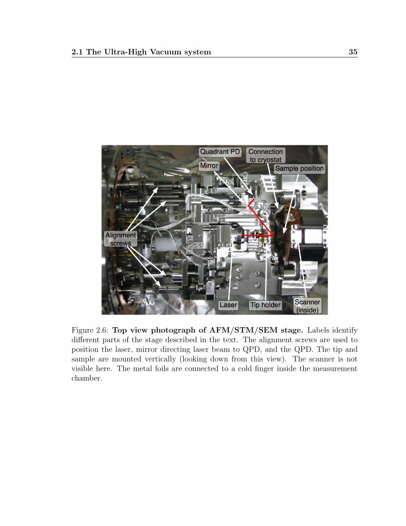
2.1 The Ultra-High Vacuum system 35
Figure 2.6: Top view photograph of AFM/STM/SEM stage. Labels identifydifferent parts of the stage described in the text. The alignment screws are used toposition the laser, mirror directing laser beam to QPD, and the QPD. The tip andsample are mounted vertically (looking down from this view). The scanner is notvisible here. The metal foils are connected to a cold finger inside the measurementchamber.
36 Chapter 2. Experimental Methods
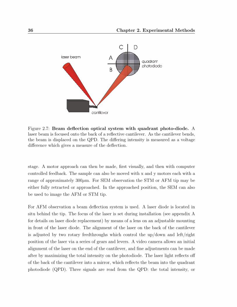
Figure 2.7: Beam deflection optical system with quadrant photo-diode. Alaser beam is focused onto the back of a reflective cantilever. As the cantilever bends,the beam is displaced on the QPD. The differing intensity is measured as a voltagedifference which gives a measure of the deflection.
stage. A motor approach can then be made, first visually, and then with computer
controlled feedback. The sample can also be moved with x and y motors each with a
range of approximately 300µm. For SEM observation the STM or AFM tip may be
either fully retracted or approached. In the approached position, the SEM can also
be used to image the AFM or STM tip.
For AFM observation a beam deflection system is used. A laser diode is located in
situ behind the tip. The focus of the laser is set during installation (see appendix A
for details on laser diode replacement) by means of a lens on an adjustable mounting
in front of the laser diode. The alignment of the laser on the back of the cantilever
is adjusted by two rotary feedthroughs which control the up/down and left/right
position of the laser via a series of gears and levers. A video camera allows an initial
alignment of the laser on the end of the cantilever, and fine adjustments can be made
after by maximizing the total intensity on the photodiode. The laser light reflects off
of the back of the cantilever into a mirror, which reflects the beam into the quadrant
photodiode (QPD). Three signals are read from the QPD: the total intensity, or
2.1 The Ultra-High Vacuum system 37
“SUM” signal, the difference between the two halves of the QPD corresponding to
the normal deflection of the cantilever, or “A-B”, and the difference between the two
halves rotated 90 corresponding to the lateral deflection of the cantilever, or “C-D”
(see fig. 2.7). The mirror rotates to adjust the position of the beam on the QPD in
the “A-B” direction, and the QPD can be adjusted up and down to center the beam
in the “C-D” direction. For beam deflection AFM systems, “A-B” is typically used
to denote the normal deflection of the beam by the cantilever, and “C-D” is typically
used to denote the lateral deflection of the beam by the cantilever.
The FE-SEM consists of two parts, the electron column containing the gun and
optics, and the detector. The electron column consists of a hot cathode Zr coated
W(100) field emission tip, and the electron optics for focusing and aligning the beam.
The electron column can also be valved off from the main chamber, and pumped
independently by a small ion pump. This helps maintain a good vacuum in both the
main imaging chamber, and the electron column.
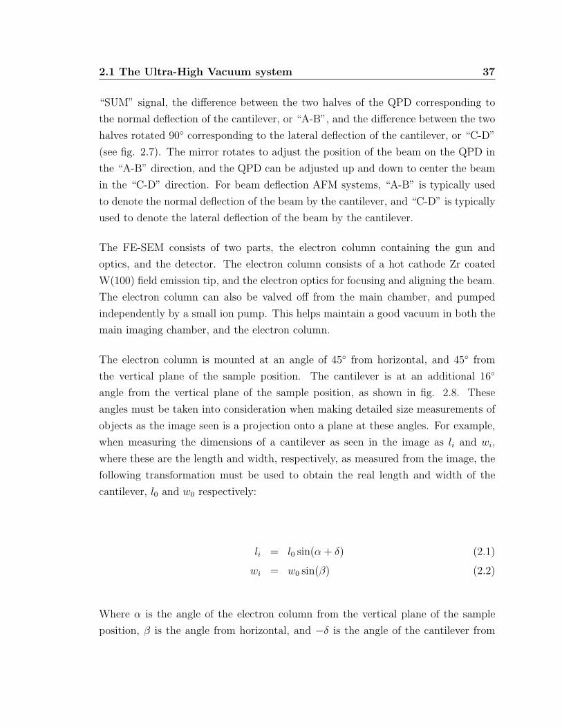
The electron column is mounted at an angle of 45 from horizontal, and 45 from
the vertical plane of the sample position. The cantilever is at an additional 16
angle from the vertical plane of the sample position, as shown in fig. 2.8. These
angles must be taken into consideration when making detailed size measurements of
objects as the image seen is a projection onto a plane at these angles. For example,
when measuring the dimensions of a cantilever as seen in the image as li and wi,
where these are the length and width, respectively, as measured from the image, the
following transformation must be used to obtain the real length and width of the
cantilever, l0 and w0 respectively:
li = l0 sin(α + δ) (2.1)
wi = w0 sin(β) (2.2)
Where α is the angle of the electron column from the vertical plane of the sample
position, β is the angle from horizontal, and −δ is the angle of the cantilever from
38 Chapter 2. Experimental Methods
Figure 2.8: Schematic of SEM view angles. The electron column is representedby the dark grey rectangle. The cantilever is represented by the light grey box in thecenter of the chamber outline. The dotted lines give the orientation of the sampleand the perpendiculars to the sample plane as a reference for the measured angles(given here in degrees).
the plane of the sample position.
The sample stage can also be cooled for observation by means of a cryotstat in
thermal contact with the sample stage via a cold finger and bundled silver foils. The
inner dewar can be filled with either liquid nitrogen (TB = 77K) or liquid helium
(TB = 4K) resulting in estimated sample temperatures of approximately 100K or
30K respectively. An outer dewar provides a cold jacket and is always filled with
liquid nitrogen when the cryostat is in use. With the outer dewar filled, the holding
time for liquid nitrogen is approximately 30 hours, and for liquid helium is 1.5-3
hours.

2.2 Description of imaging modes used 39
2.2 Description of imaging modes used
Two primary modes of atomic force microscopy imaging were employed herein, “con-
tact” mode, and “non-contact” mode, or frequency detection AFM. The STM mode
was also tested, but not used here as all of the sample substrates were insulating.
2.2.1 Contact-mode AFM imaging
As discussed briefly in the previous chapter, contact mode AFM creates an image of
a surface by raster scanning a sharp tip attached to a force sensor across a surface
and recording the force related signals. There are different methods of sensing the
force between the tip and a surface, however, the beam deflection approach with a
quadrant photo-diode (QPD) is used here. In this case, as the tip is scanned over
the surface, the static deflection of the cantilever is measured by the deflection of the
laser beam on the QPD as a voltage in the “A-B” direction, or VA−B. This voltage
is used as a feedback parameter to minimize the deviation of VA−B from the desired
set-point. For greatest sensitivity, the QPD should be aligned such that VA−B is close
to zero during normal imaging conditions. The piezo-electric scanner moves in the z
direction, ie. changes the separation distance between the tip and sample to maintain
this constant deflection, and thus a constant force. The z-movement of the piezo is
recorded as a function of the x and y positions of the piezo producing a topography
which can then be displayed by the computer.
A quantitative calibration of the normal force can be performed by finding the re-
lationship between VA−B and the deflection of the cantilever, and by calculating the
spring constant of the cantilever. The former can be found by performing a force
vs. distance measurement which moves the piezo at constant rate towards and away
from the sample and measures the deflection of the cantilever. This gives a relation
between distance and voltage on the QPD, which we will call the sensitivity, sz, of
the combined cantilever and photo-diode system. It should be noted that both the
approach and retract directions are usually measured, so that any adhesive effects
are observed and excluded for the purpose of calibration. In this way, the normal
40 Chapter 2. Experimental Methods
force exerted on and by the cantilever can be expressed in the following way [46]:
FN = cNszVA−B (2.3)
where FN is the normal force, cN is the spring constant of the normal mode of the
cantilever, sz is the aforementioned sensitivity in V/m, and VA−B is the voltage on
the QPD in the “A-B” direction. It should be noted here, that for proper calculation
of the force VA−B as used in the equation above should be the difference between the
voltage during imaging, and the “zero” force voltage, ie. the QPD voltage when the
tip is retracted. The spring constant associated with the normal bending mode of a
rectangular cantilever can be expressed as [46, 47]:
cN =Ewt3
4l3(2.4)
where E is the elastic modulus of the cantilever material, w is the width of the
cantilever, t is the thickness of the cantilever, and l is the length of the cantilever.
Generally, the length and width of the cantilever specified by the manufacturer are
sufficiently accurate to calculate the spring constant, but can be measured with an
SEM to obtain greater accuracy. However, the thickness of microfabricated can-
tilevers can vary widely, and as cN goes as the cube of the thickhess, it should be
obtained to greater accuracy. The simplest method of determining the thickness of
the cantilever is from the resonance frequency [48]:
t =4√
3πl2
1.8732f0
√ρ
E(2.5)
where f0 is the resonance frequency of the cantilever, l is again the length, ρ is the
density of the material, and E is again the elastic modulus of the material. For
silicon, the values of the elastic modulus and the density are ESi = 1.69× 10¹¹N/m2
and ρ = 2.33× 10³kg/m3 respectively [49].
2.2 Description of imaging modes used 41
A secondary mode of contact mode imaging is lateral force AFM (LF-AFM), or
friction force microscopy (FFM). This mode is possible with a QPD as the lateral
deflection of the cantilever can be recorded simultaneously with the normal mode in-
formation. Other optical detection schemes cannot measure lateral or friction forces.
In LF-AFM mode, the scan direction is rotated by 90 from the usual scanning di-
rection to maximize the lateral forces on the cantilever (see fig. 3.5). The same
contact mode imaging as described above is performed, but now the “C-D” signal
on the QPD is also recorded corresponding to the lateral forces exerted on and by
the cantilever. As with the normal forces, the lateral forces can be quantified. The
lateral, or torsional, force can be expressed as [46]:
FT =3
2cT
h
lszVC−D (2.6)
where FT is the torsional force, cT is the torsional spring constant, h is the height of
the tip, l is the length of the cantilever, sz is the sensitivity of the QPD as above, and
VC−D is the voltage signal of the QPD in the “C-D” direction. The factors of 3/2 and
h/l compensate for the twisting of the cantilever and that the laser is not focused on
the pivot of this motion (the tip apex) but on the back of the cantilever above the
position of the tip. For a rectangular cantilever, the torsional spring constant can be
expressed by the following [46]:
cT =Gwt3
3h2l(2.7)
where G is the shear modulus of the material of the cantilever, w is the width, t is
the thickness, h is the height of the tip, and l is the length of the cantilever. For
silicon, the value of the shear modulus is GSi = 0.68× 10¹¹N/m [49].
As the lateral forces measured can be quite small, an amplifier (by Stanford Applied
Research) was used on the VC−D output signal before recording it with the computer
software. Gain settings of 20×, 50×, and 100× were used depending on the total
range of the signal, and a low pass filter was used.
42 Chapter 2. Experimental Methods
2.2.2 Non-contact AFM imaging
As described briefly in the previous chapter, non-contact AFM (NC-AFM) operates
in a similar manner to contact mode AFM, whereby a sharp tip is raster scanned
over a surface and a parameter related to the interaction between the tip and sample
is measured. As opposed to contact mode, where a static deflection is measured,
the tip is made to oscillate and a shift in the resonance frequency of the tip-sample
system is measured. An oscillatory drive signal is applied to the small piezo under
the cantilever chip (as described previously) causing the cantilever to oscillate. The
same beam deflection system used for contact mode imaging is used to measure the
oscillation of the cantilever in the “A-B” channel, and the “C-D” is centered to zero
and is not expected to show much variation. Both the excitation of the cantilever,
and the frequency measurement are performed by a phase-locked loop (PLL).
A simplified block diagram of the frequency detection and excitation signal production
electronics of the NanoSurf PLL used for the experiments described herein can be
found in fig. 2.9 [50]. The PLL takes the oscillating “A-B” signal of the QPD as
the input frequency. The phase of this signal is then compared to the phase of the
output signal of the voltage controlled oscillator (VCO). The multiplier and low-pass
filter act as this phase comparator, as indicated in the figure by the grey dotted line.
The output of the phase comparator, Uphase is given by [50]:
Uphase ∝ cos(φin − φref ) (2.8)
where φin is the phase of the input signal, and φref is the phase of the VCO output
signal. A proportional-integral (PI) gain controller provides feedback on this phase
comparison such that the VCO has the same frequency as the input signal, and thus
there is a constant 90 phase shift between the input signal and the VCO output. The
PLL is then in the “phase-locked” state, hence the term “phase-locked loop”. While
in the locked stated, the PLL can measure small changes in the input frequency in the
same way by adjusting the VCO output to accommodate the shift in frequency. The
output is a DC representation of the difference between the measured frequency and
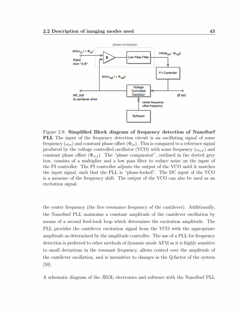
2.2 Description of imaging modes used 43
Figure 2.9: Simplified Block diagram of frequency detection of NanoSurfPLL The input of the frequency detection circuit is an oscillating signal of somefrequency (ωin) and constant phase offset (Φin). This is compared to a reference signalproduced by the voltage controlled oscillator (VCO) with some frequency (ωref ) andconstant phase offset (Φref ). The “phase comparator”, outlined in the dotted greybox, consists of a multiplier and a low pass filter to reduce noise on the input ofthe PI controller. The PI controller adjusts the output of the VCO until it matchesthe input signal, such that the PLL is “phase-locked”. The DC input of the VCOis a measure of the frequency shift. The output of the VCO can also be used as anexcitation signal.
the center frequency (the free resonance frequency of the cantilever). Additionally,
the NanoSurf PLL maintains a constant amplitude of the cantilever oscillation by
means of a second feed-back loop which determines the excitation amplitude. The
PLL provides the cantilever excitation signal from the VCO with the appropriate
amplitude as determined by the amplitude controller. The use of a PLL for frequency
detection is preferred to other methods of dynamic mode AFM as it is highly sensitive
to small deviations in the resonant frequency, allows control over the amplitude of
the cantilever oscillation, and is insensitive to changes in the Q-factor of the system
[50].
A schematic diagram of the JEOL electronics and software with the NanoSurf PLL
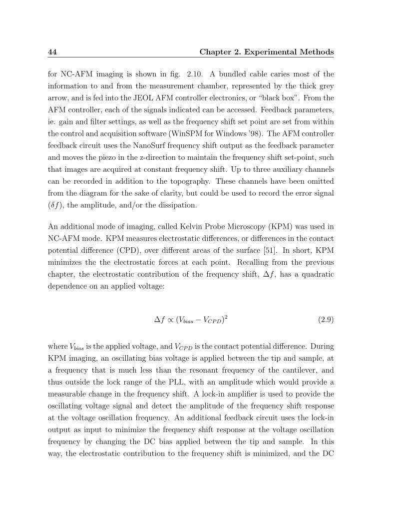
44 Chapter 2. Experimental Methods
for NC-AFM imaging is shown in fig. 2.10. A bundled cable caries most of the
information to and from the measurement chamber, represented by the thick grey
arrow, and is fed into the JEOL AFM controller electronics, or “black box”. From the
AFM controller, each of the signals indicated can be accessed. Feedback parameters,
ie. gain and filter settings, as well as the frequency shift set point are set from within
the control and acquisition software (WinSPM for Windows ’98). The AFM controller
feedback circuit uses the NanoSurf frequency shift output as the feedback parameter
and moves the piezo in the z-direction to maintain the frequency shift set-point, such
that images are acquired at constant frequency shift. Up to three auxiliary channels
can be recorded in addition to the topography. These channels have been omitted
from the diagram for the sake of clarity, but could be used to record the error signal
(δf), the amplitude, and/or the dissipation.
An additional mode of imaging, called Kelvin Probe Microscopy (KPM) was used in
NC-AFM mode. KPM measures electrostatic differences, or differences in the contact
potential difference (CPD), over different areas of the surface [51]. In short, KPM
minimizes the the electrostatic forces at each point. Recalling from the previous
chapter, the electrostatic contribution of the frequency shift, ∆f , has a quadratic
dependence on an applied voltage:
∆f ∝ (Vbias − VCPD)2 (2.9)
where Vbias is the applied voltage, and VCPD is the contact potential difference. During
KPM imaging, an oscillating bias voltage is applied between the tip and sample, at
a frequency that is much less than the resonant frequency of the cantilever, and
thus outside the lock range of the PLL, with an amplitude which would provide a
measurable change in the frequency shift. A lock-in amplifier is used to provide the
oscillating voltage signal and detect the amplitude of the frequency shift response
at the voltage oscillation frequency. An additional feedback circuit uses the lock-in
output as input to minimize the frequency shift response at the voltage oscillation
frequency by changing the DC bias applied between the tip and sample. In this
way, the electrostatic contribution to the frequency shift is minimized, and the DC
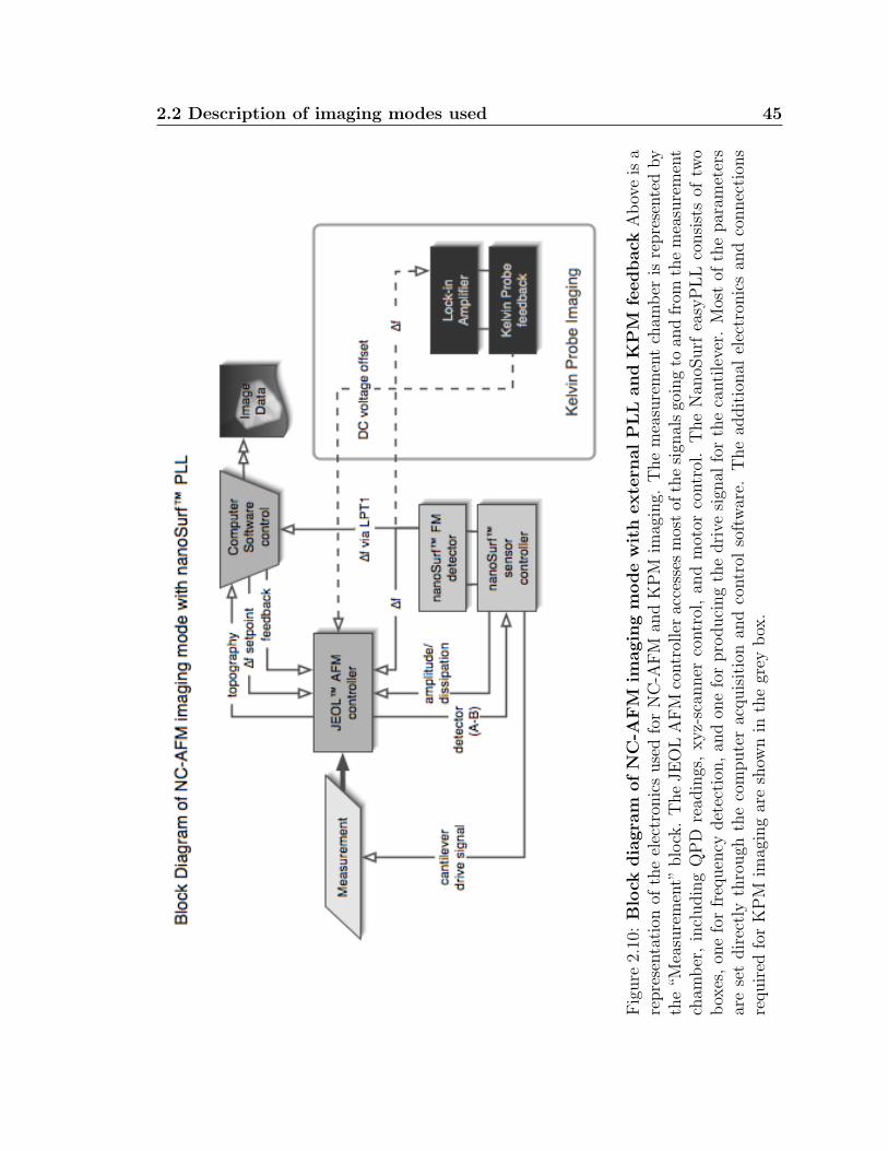
2.2 Description of imaging modes used 45
Fig
ure
2.10
:B
lock
dia
gra
mofN
C-A
FM
imagin
gm
ode
with
exte
rnalP
LL
and
KP
Mfe
edback
Abov
eis
are
pre
senta
tion
ofth
eel
ectr
onic
suse
dfo
rN
C-A
FM
and
KP
Mim
agin
g.T
he
mea
sure
men
tch
amber
isre
pre
sente
dby
the
“Mea
sure
men
t”blo
ck.
The
JE
OL
AFM
contr
olle
rac
cess
esm
ostof
the
sign
alsgo
ing
toan
dfr
omth
em
easu
rem
ent
cham
ber
,in
cludin
gQ
PD
read
ings
,xyz-
scan
ner
contr
ol,an
dm
otor
contr
ol.
The
Nan
oSurf
easy
PLL
consi
sts
oftw
obox
es,on
efo
rfr
equen
cydet
ecti
on,an
don
efo
rpro
duci
ng
the
dri
vesi
gnal
for
the
canti
leve
r.M
ost
ofth
epar
amet
ers
are
set
dir
ectl
yth
rough
the
com
pute
rac
quis
itio
nan
dco
ntr
olso
ftw
are.
The
additio
nal
elec
tron
ics
and
connec
tion
sre
quired
for
KP
Mim
agin
gar
esh
own
inth
egr
eybox
.
46 Chapter 2. Experimental Methods
Figure 2.11: Illustration of Kelvin Probe imaging. The top left image is anillustration of a topographic AFM image of two materials, A and B, B being ofgreater height (white) than A (dark grey). The top right image shows what theKelvin Probe image might look like if the CPD of B was less than the CPD of A, ascan be seen in the frequency shift vs. voltage relation for each plotted below.
bias used to achieve this is a measure of the contact potential difference between the
tip and the different sample areas (see fig. 2.11). It has also been put forth that
the topography obtained while the KPM feedback is active is the “true” topography
of the sample as the electrostatic forces are minimized over heterogeneous samples
[52]. A schematic of the KPM electronics is included in fig. 2.10, with the additional
electronics for KPM inside the grey box, and the additional connections for the lock-in
amplifier and Kelvin Probe feedback circuit shown with dashed lines.
Chapter 3
KBr substrate preparation and
characterization
3.1 Preparation of the KBr(001) surface
Blocks of pure, optical quality, unpolished KBr crystal were obtained from Korth
Krystalle. The pieces were cleaved along the 100 directions to the appropriate
size for use in the cleaving holder described in the previous chapter. Air-cleaved
samples were cleaved using a sharp, clean razor blade, with the sample mounted in the
cleaving holder. The cleaved surface was exposed to air for no longer than 30s before
introduction to the load-lock and pumping. Once inside the preparation chamber,
samples were heated for 1-2 hours using a quartz lamp directed at the surface through
a window to remove any surface contamination that may have accumulated. For
vacuum cleaved samples, the crystal was mounted in the sample holder and a line
was lightly scribed in the <100> direction with a clean razor blade. The crystal was
then introduced to the vacuum system through the load-lock. Once in the preparation
chamber, the sample was cleaved using the cleaving station described in the previous
chapter. The sample was then heated with the heating parent holder (described in
the previous chapter) for 1 hour at ∼ 150C to remove residual charge from the
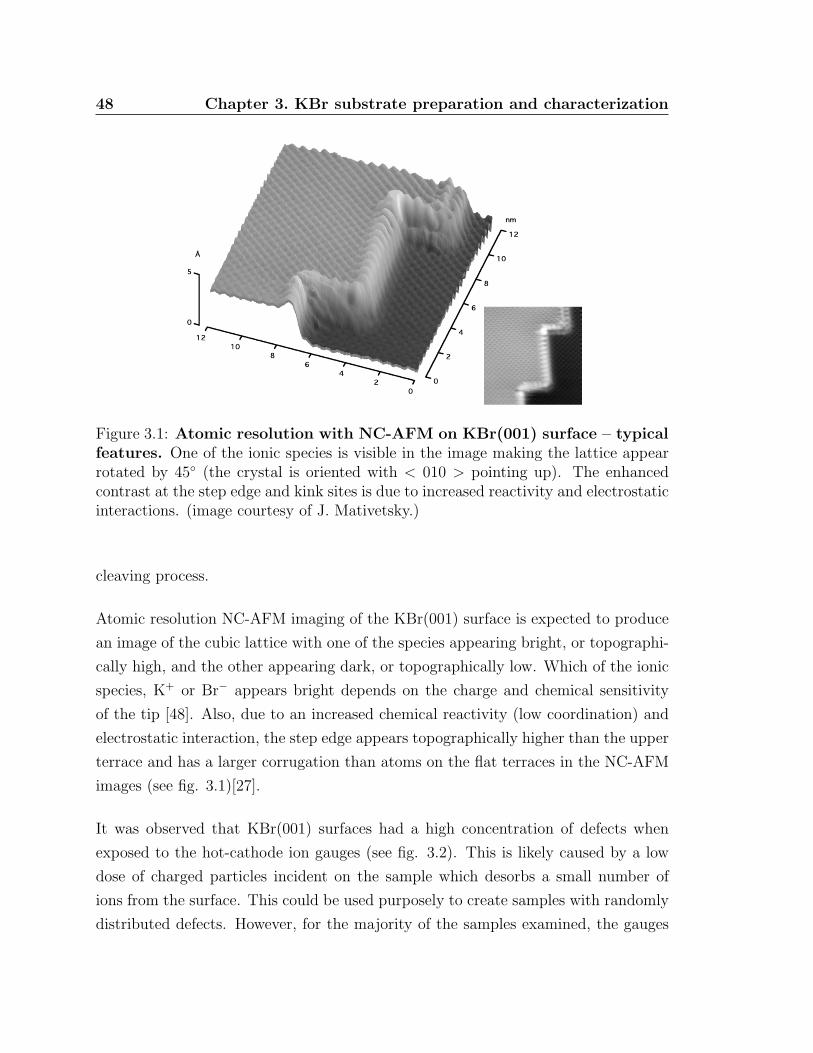
48 Chapter 3. KBr substrate preparation and characterization
Figure 3.1: Atomic resolution with NC-AFM on KBr(001) surface – typicalfeatures. One of the ionic species is visible in the image making the lattice appearrotated by 45 (the crystal is oriented with < 010 > pointing up). The enhancedcontrast at the step edge and kink sites is due to increased reactivity and electrostaticinteractions. (image courtesy of J. Mativetsky.)
cleaving process.
Atomic resolution NC-AFM imaging of the KBr(001) surface is expected to produce
an image of the cubic lattice with one of the species appearing bright, or topographi-
cally high, and the other appearing dark, or topographically low. Which of the ionic
species, K+ or Br− appears bright depends on the charge and chemical sensitivity
of the tip [48]. Also, due to an increased chemical reactivity (low coordination) and
electrostatic interaction, the step edge appears topographically higher than the upper
terrace and has a larger corrugation than atoms on the flat terraces in the NC-AFM
images (see fig. 3.1)[27].
It was observed that KBr(001) surfaces had a high concentration of defects when
exposed to the hot-cathode ion gauges (see fig. 3.2). This is likely caused by a low
dose of charged particles incident on the sample which desorbs a small number of
ions from the surface. This could be used purposely to create samples with randomly
distributed defects. However, for the majority of the samples examined, the gauges
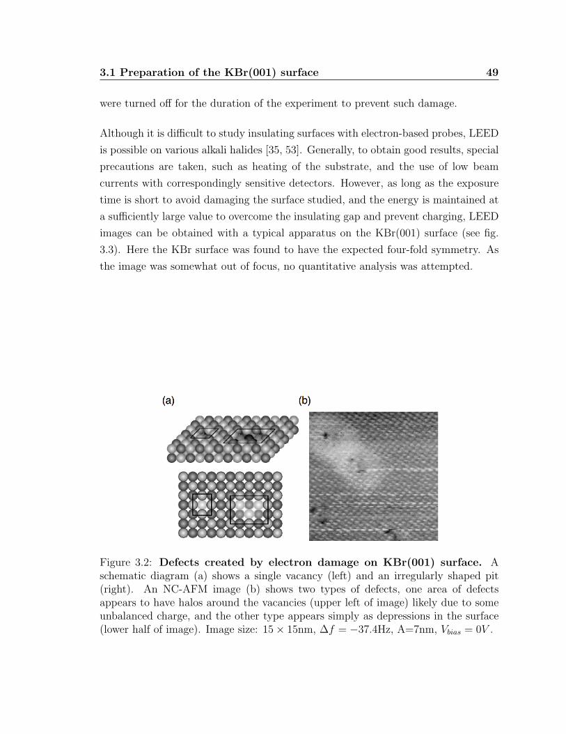
3.1 Preparation of the KBr(001) surface 49
were turned off for the duration of the experiment to prevent such damage.
Although it is difficult to study insulating surfaces with electron-based probes, LEED
is possible on various alkali halides [35, 53]. Generally, to obtain good results, special
precautions are taken, such as heating of the substrate, and the use of low beam
currents with correspondingly sensitive detectors. However, as long as the exposure
time is short to avoid damaging the surface studied, and the energy is maintained at
a sufficiently large value to overcome the insulating gap and prevent charging, LEED
images can be obtained with a typical apparatus on the KBr(001) surface (see fig.
3.3). Here the KBr surface was found to have the expected four-fold symmetry. As
the image was somewhat out of focus, no quantitative analysis was attempted.
Figure 3.2: Defects created by electron damage on KBr(001) surface. Aschematic diagram (a) shows a single vacancy (left) and an irregularly shaped pit(right). An NC-AFM image (b) shows two types of defects, one area of defectsappears to have halos around the vacancies (upper left of image) likely due to someunbalanced charge, and the other type appears simply as depressions in the surface(lower half of image). Image size: 15× 15nm, ∆f = −37.4Hz, A=7nm, Vbias = 0V .
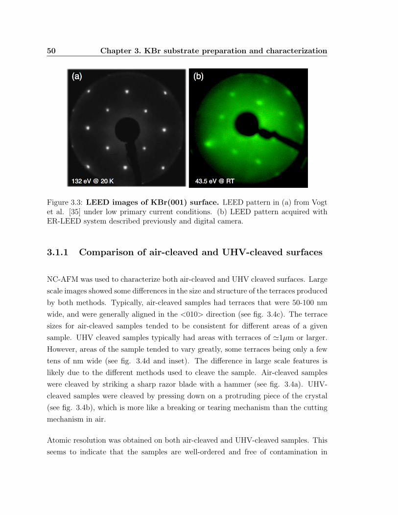
50 Chapter 3. KBr substrate preparation and characterization
Figure 3.3: LEED images of KBr(001) surface. LEED pattern in (a) from Vogtet al. [35] under low primary current conditions. (b) LEED pattern acquired withER-LEED system described previously and digital camera.
3.1.1 Comparison of air-cleaved and UHV-cleaved surfaces
NC-AFM was used to characterize both air-cleaved and UHV cleaved surfaces. Large
scale images showed some differences in the size and structure of the terraces produced
by both methods. Typically, air-cleaved samples had terraces that were 50-100 nm
wide, and were generally aligned in the <010> direction (see fig. 3.4c). The terrace
sizes for air-cleaved samples tended to be consistent for different areas of a given
sample. UHV cleaved samples typically had areas with terraces of '1µm or larger.
However, areas of the sample tended to vary greatly, some terraces being only a few
tens of nm wide (see fig. 3.4d and inset). The difference in large scale features is
likely due to the different methods used to cleave the sample. Air-cleaved samples
were cleaved by striking a sharp razor blade with a hammer (see fig. 3.4a). UHV-
cleaved samples were cleaved by pressing down on a protruding piece of the crystal
(see fig. 3.4b), which is more like a breaking or tearing mechanism than the cutting
mechanism in air.
Atomic resolution was obtained on both air-cleaved and UHV-cleaved samples. This
seems to indicate that the samples are well-ordered and free of contamination in
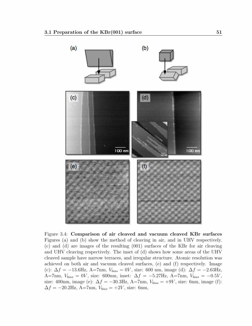
3.1 Preparation of the KBr(001) surface 51
Figure 3.4: Comparison of air cleaved and vacuum cleaved KBr surfacesFigures (a) and (b) show the method of cleaving in air, and in UHV respectively.(c) and (d) are images of the resulting (001) surfaces of the KBr for air cleavingand UHV cleaving respectively. The inset of (d) shows how some areas of the UHVcleaved sample have narrow terraces, and irregular structure. Atomic resolution wasachieved on both air and vacuum cleaved surfaces, (e) and (f) respectively. Image(c): ∆f = −13.6Hz, A=7nm, Vbias = 0V , size: 600 nm, image (d): ∆f = −2.63Hz,A=7nm, Vbias = 0V , size: 600nm, inset: ∆f = −5.27Hz, A=7nm, Vbias = −0.5V ,size: 400nm, image (e): ∆f = −30.3Hz, A=7nm, Vbias = +9V , size: 6nm, image (f):∆f = −20.2Hz, A=7nm, Vbias = +2V , size: 6nm,
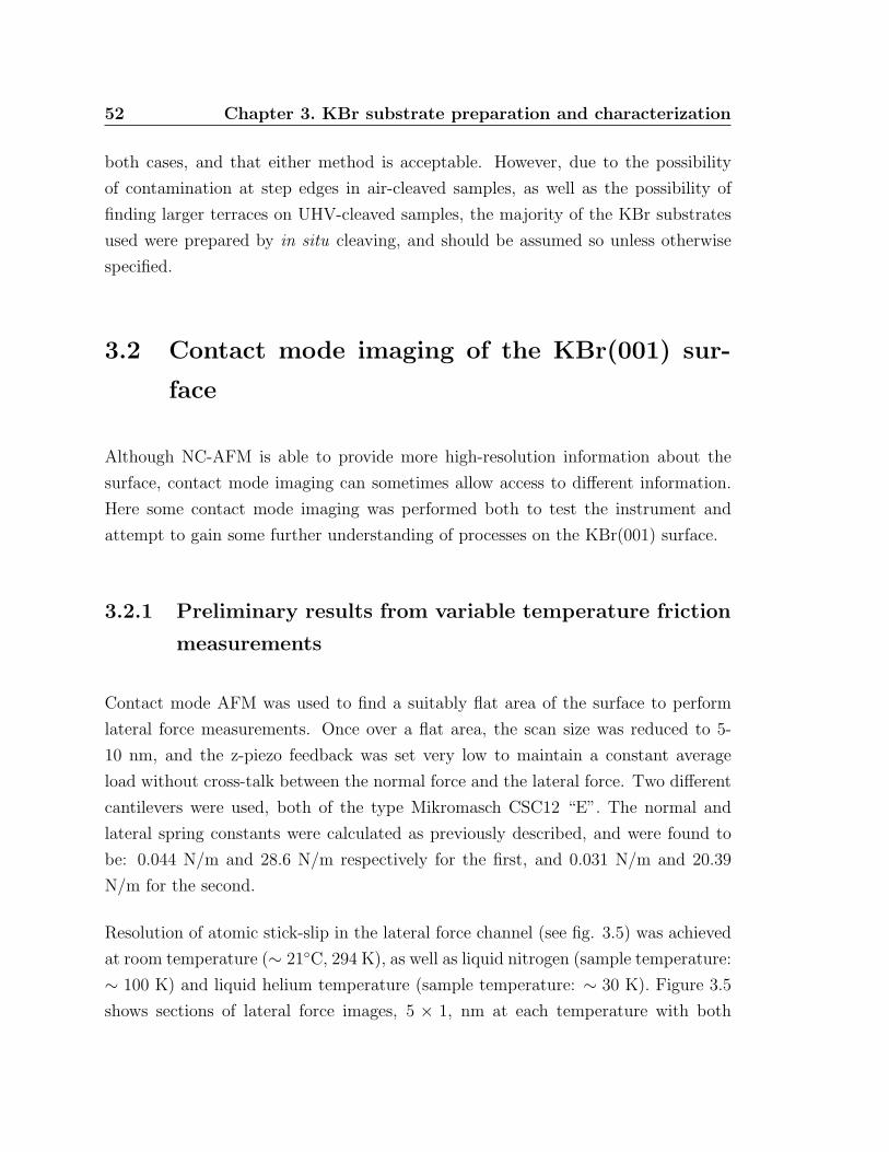
52 Chapter 3. KBr substrate preparation and characterization
both cases, and that either method is acceptable. However, due to the possibility
of contamination at step edges in air-cleaved samples, as well as the possibility of
finding larger terraces on UHV-cleaved samples, the majority of the KBr substrates
used were prepared by in situ cleaving, and should be assumed so unless otherwise
specified.
3.2 Contact mode imaging of the KBr(001) sur-
face
Although NC-AFM is able to provide more high-resolution information about the
surface, contact mode imaging can sometimes allow access to different information.
Here some contact mode imaging was performed both to test the instrument and
attempt to gain some further understanding of processes on the KBr(001) surface.
3.2.1 Preliminary results from variable temperature friction
measurements
Contact mode AFM was used to find a suitably flat area of the surface to perform
lateral force measurements. Once over a flat area, the scan size was reduced to 5-
10 nm, and the z-piezo feedback was set very low to maintain a constant average
load without cross-talk between the normal force and the lateral force. Two different
cantilevers were used, both of the type Mikromasch CSC12 “E”. The normal and
lateral spring constants were calculated as previously described, and were found to
be: 0.044 N/m and 28.6 N/m respectively for the first, and 0.031 N/m and 20.39
N/m for the second.
Resolution of atomic stick-slip in the lateral force channel (see fig. 3.5) was achieved
at room temperature (∼ 21C, 294 K), as well as liquid nitrogen (sample temperature:
∼ 100 K) and liquid helium temperature (sample temperature: ∼ 30 K). Figure 3.5
shows sections of lateral force images, 5 × 1, nm at each temperature with both
3.2 Contact mode imaging of the KBr(001) surface 53
Figure 3.5: FFM images at liquid He, liquid N, and room temperature.Partial mirror images at top show forward and backscan on each line. Selections are1×5 nm each. Starting from top: room temperature (21C), FN = 0.39nN, liquidnitrogen temperature (∼ 100K), FN = −0.45nN, liquid helium temperature (∼ 30K),FN = −1.00nN. Friction loops shown below taken from cross-section marked on eachpartial image above for corresponding temperature and load.

54 Chapter 3. KBr substrate preparation and characterization
the forward (left half) and back (right half) scan, ie. when the tip is moving to
the right and to the left respectively. The marked cross-sections are also shown,
displaying clearly the stick-slip motion of the tip over each atom. Hysteresis was also
observed, indicating that some energy is dissipated into the surface, particularly for
the low temperature traces. Note, however, that the loads for the low temperature
images are increasingly strong in the “pulling” direction (cantilever is bent towards
the surface due to an attractive force). This was due to an observed increase in the
adhesion of the tip to the surface at these temperatures. However, since the loads were
ill-defined due to drift in the z direction, especially at low temperatures, statements
regarding the temperature dependence of the friction force will be reserved for further
experiments. Drift was also apparent in the slow scan direction (y-direction) as can
be seen by the “squashed” appearance of the KBr lattice in the images in figure 3.5,
however, this could be corrected during the scan process, and does not effect the
ability to define the forces, and is thus of less importance than the drift in the normal
force.
Despite the problems encountered, the variable temperature measurements could be
obtained, and the forces measured are on the order of tenths of nN, demonstrating
that the instrument functions over a temperature range of 30–300 K with a sufficient
sensitivity for this type of measurement. Further investigation of friction phenomena
at variable temperature should be performed to confirm the functional dependance
of atomic scale friction forces on temperature [54]. Although quantitative friction
measurements were made difficult by drift, the ability to measure the small lateral
forces involved in atomic stick-slip motion points to the possibility of measuring
lateral forces during molecular manipulation investigations.
3.2.2 Preliminary results of ESD modification of KBr by
SEM
Recent NC-AFM measurements of Sub-PC on electron irradiated KBr have suggested
that the nanometer size pits produced by electron exposure could be used as a “nano-
patterning” technique to confine small numbers of molecules [55]. Here, the possibility
3.2 Contact mode imaging of the KBr(001) surface 55
of using the in-situ SEM to expose a small area of the KBr surface is investigated for
potential patterning applications.
Contact mode imaging was used to characterize the air-cleaved KBr surface prior to
exposure to the SEM electron beam. Figure 3.6 shows the contact mode topogra-
phy (a) and lateral force (b) images before electron irradiation. The tip was then
retracted with the piezo and the shutter to the SEM column opened slightly to aim
the electron beam near the tip position. Once the electron beam was positioned and
switched to a high magnification to reduce the exposure area, the shutter was opened
completely for a short period of time. The electron beam produced by the SEM had
an emission current of 84µA at an acceleration voltage of 10 keV. The sample was at
room temperature and was not heated after irradiation.
After electron irradiation, the same area of the surface was imaged by re-approaching
the tip. Although large scale features of the surface were still visible, the general
appearance of the surface became much more rough and irregular after electron ex-
posure as seen in both the topography (fig. 3.6c) and lateral force image (fig. 3.6d).
Depressions in the surface are 10-20 nm deep, indicating that many layers of the KBr
were affected by the electron beam. The general appearance of the surface seems con-
sistent with images from electron stimulated desorption experiments on KBr where
approximately half a monolayer of the surface is removed (transition between pits
and islands) [56, 57, 58]. However, in these previous experiments, desorption occured
layer-by-layer such that the pits were only a single atomic layer deep. The more
rounded appearance of the structures imaged here are likely due to tip convolutions.
To determine whether the effects were localized or not, the tip was retracted and
moved ∼10µm. This new area was imaged and appeared unaffected by the previous
irradiation (see fig. 3.7a and b). The irradiation procedure was repeated on this
area giving similar results (see fig. 3.7c and d). The damaged surface was repeatedly
imaged causing a rearrangement of the surface into rows perpendicular to the fast
scan direction. This “ripple” formation has been observed in polymer systems [59]
and was recently observed on atomically flat KBr(001) surfaces, ie. surfaces that were
not previously modified [60]. The wavelength of the ripple pattern on KBr has been
found to correspond to the radius of the AFM tip [60], indicating here that the tip
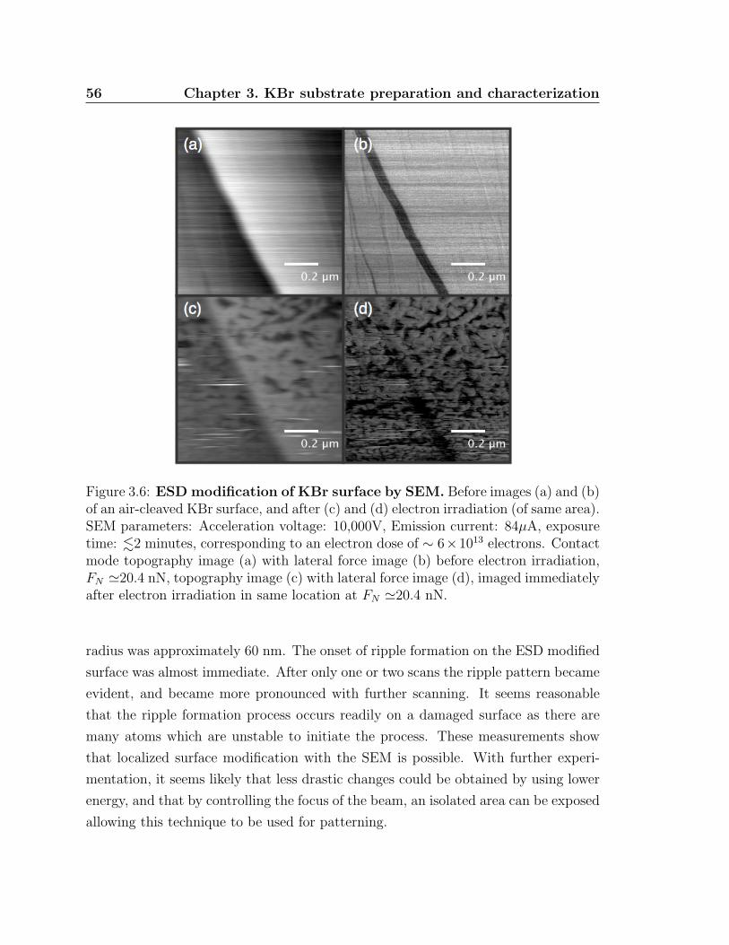
56 Chapter 3. KBr substrate preparation and characterization
Figure 3.6: ESD modification of KBr surface by SEM. Before images (a) and (b)of an air-cleaved KBr surface, and after (c) and (d) electron irradiation (of same area).SEM parameters: Acceleration voltage: 10,000V, Emission current: 84µA, exposuretime: .2 minutes, corresponding to an electron dose of ∼ 6×10¹³ electrons. Contactmode topography image (a) with lateral force image (b) before electron irradiation,FN '20.4 nN, topography image (c) with lateral force image (d), imaged immediatelyafter electron irradiation in same location at FN '20.4 nN.
radius was approximately 60 nm. The onset of ripple formation on the ESD modified
surface was almost immediate. After only one or two scans the ripple pattern became
evident, and became more pronounced with further scanning. It seems reasonable
that the ripple formation process occurs readily on a damaged surface as there are
many atoms which are unstable to initiate the process. These measurements show
that localized surface modification with the SEM is possible. With further experi-
mentation, it seems likely that less drastic changes could be obtained by using lower
energy, and that by controlling the focus of the beam, an isolated area can be exposed
allowing this technique to be used for patterning.
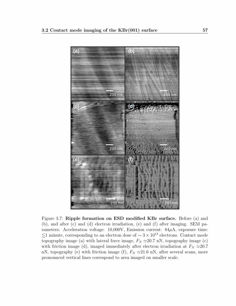
3.2 Contact mode imaging of the KBr(001) surface 57
Figure 3.7: Ripple formation on ESD modified KBr surface. Before (a) and(b), and after (c) and (d) electron irradiation, (e) and (f) after imaging. SEM pa-rameters: Acceleration voltage: 10,000V, Emission current: 84µA, exposure time:.1 minute, corresponding to an electron dose of ∼ 3× 10¹³ electrons. Contact modetopography image (a) with lateral force image, FN '20.7 nN, topography image (c)with friction image (d), imaged immediately after electron irradiation at FN '20.7nN, topography (e) with friction image (f), FN '21.6 nN, after several scans, morepronounced vertical lines correspond to area imaged on smaller scale.
Chapter 4
C60 on KBr – imaging and growth
characteristics
4.1 Deposition of C60 molecules on the KBr(001)
surface
The KBr(001) surface was prepared as described in the previous chapter and char-
acterized prior to the deposition of molecular material. The C60 molecules were
obtained from Alfa Aesar and had a specified purity of 99.9+%. Additional purifi-
cation is achieved by outgassing the source in UHV at 220C for a period of ∼14
hours. C60 molecules were deposited via thermal evaporation by the molecule evap-
orator described in chapter 2 on to a room temperature substrate. Typically, the
deposition temperature was 330C. A temperature dependence plot of the deposi-
tion rate, measured with the quartz microbalance described previously, is given in
figure 4.1, though the deposition rate was also dependent on the source and shutter
position. Adjustment of the shutter to reduce the rate of evaporation was chosen
rather than altering the temperature to avoid also changing the kinetic energy of the
deposited material. Rates used ranged from 0.0015 ML/s to 0.0077 ML/s. A list of
rates, deposition times and coverages used for different samples is given in table 4.1.
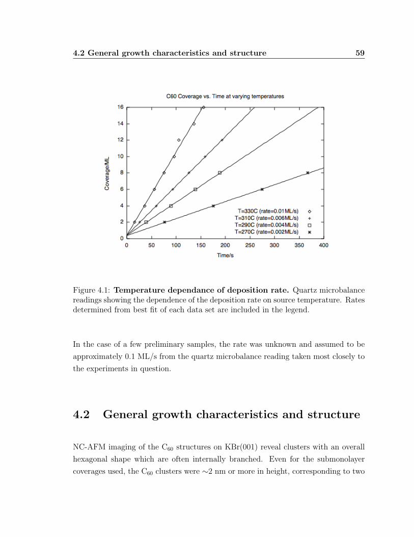
4.2 General growth characteristics and structure 59
Figure 4.1: Temperature dependance of deposition rate. Quartz microbalancereadings showing the dependence of the deposition rate on source temperature. Ratesdetermined from best fit of each data set are included in the legend.
In the case of a few preliminary samples, the rate was unknown and assumed to be
approximately 0.1 ML/s from the quartz microbalance reading taken most closely to
the experiments in question.
4.2 General growth characteristics and structure
NC-AFM imaging of the C60 structures on KBr(001) reveal clusters with an overall
hexagonal shape which are often internally branched. Even for the submonolayer
coverages used, the C60 clusters were ∼2 nm or more in height, corresponding to two
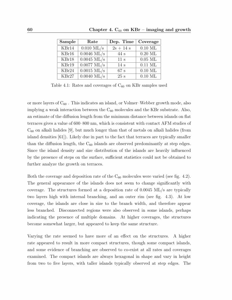
60 Chapter 4. C60 on KBr – imaging and growth
Sample Rate Dep. Time Coverage
KBr14 0.010 ML/s 2s + 14 s 0.10 MLKBr16 0.0046 ML/s 44 s 0.20 MLKBr18 0.0045 ML/s 11 s 0.05 MLKBr19 0.0077 ML/s 14 s 0.11 MLKBr24 0.0015 ML/s 67 s 0.10 MLKBr27 0.0040 ML/s 25 s 0.10 ML
Table 4.1: Rates and coverages of C60 on KBr samples used
or more layers of C60 . This indicates an island, or Volmer–Webber growth mode, also
implying a weak interaction between the C60 molecules and the KBr substrate. Also,
an estimate of the diffusion length from the minimum distance between islands on flat
terraces gives a value of 600–800 nm, which is consistent with contact AFM studies of
C60 on alkali halides [9], but much longer than that of metals on alkali halides (from
island densities [61]). Likely due in part to the fact that terraces are typically smaller
than the diffusion length, the C60 islands are observed predominantly at step edges.
Since the island density and size distribution of the islands are heavily influenced
by the presence of steps on the surface, sufficient statistics could not be obtained to
further analyze the growth on terraces.
Both the coverage and deposition rate of the C60 molecules were varied (see fig. 4.2).
The general appearance of the islands does not seem to change significantly with
coverage. The structures formed at a deposition rate of 0.0045 ML/s are typically
two layers high with internal branching, and an outer rim (see fig. 4.3). At low
coverage, the islands are close in size to the branch width, and therefore appear
less branched. Disconnected regions were also observed in some islands, perhaps
indicating the presence of multiple domains. At higher coverages, the structures
become somewhat larger, but appeared to keep the same structure.
Varying the rate seemed to have more of an effect on the structures. A higher
rate appeared to result in more compact structures, though some compact islands,
and some evidence of branching are observed to co-exist at all rates and coverages
examined. The compact islands are always hexagonal in shape and vary in height
from two to five layers, with taller islands typically observed at step edges. The
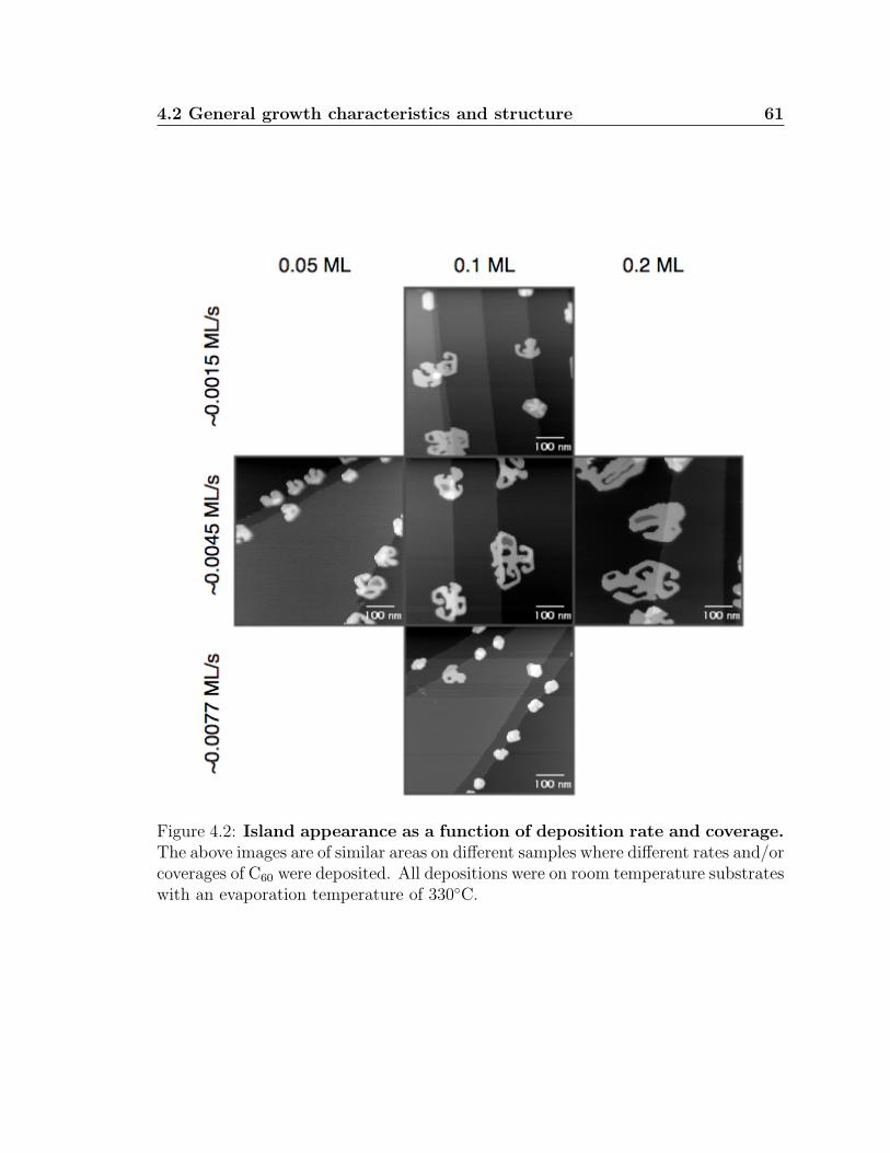
4.2 General growth characteristics and structure 61
Figure 4.2: Island appearance as a function of deposition rate and coverage.The above images are of similar areas on different samples where different rates and/orcoverages of C60 were deposited. All depositions were on room temperature substrateswith an evaporation temperature of 330C.
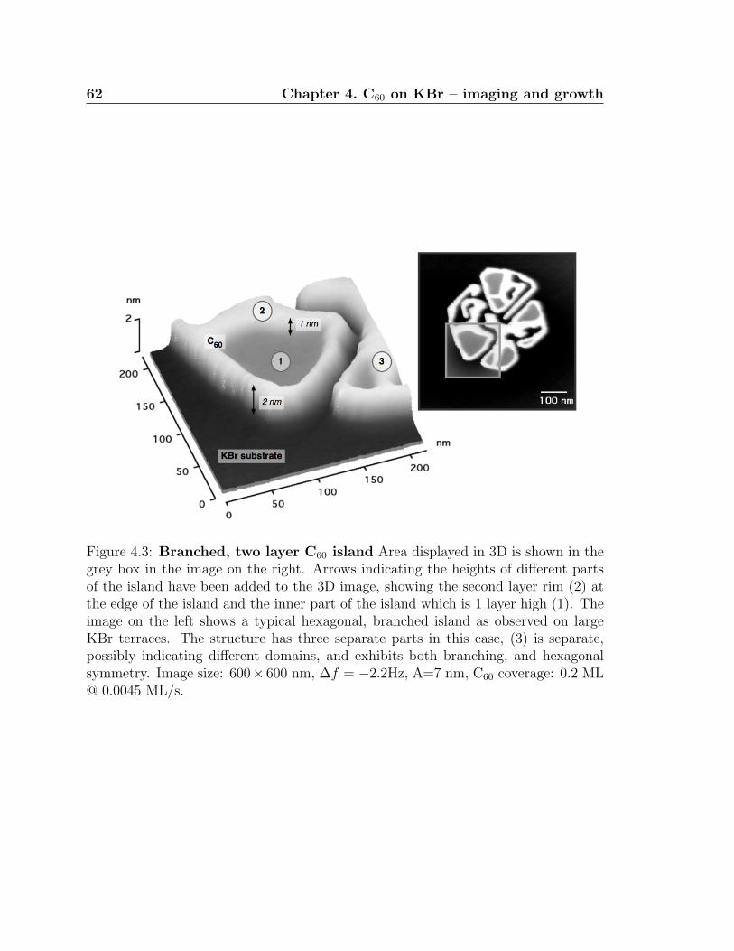
62 Chapter 4. C60 on KBr – imaging and growth
Figure 4.3: Branched, two layer C60 island Area displayed in 3D is shown in thegrey box in the image on the right. Arrows indicating the heights of different partsof the island have been added to the 3D image, showing the second layer rim (2) atthe edge of the island and the inner part of the island which is 1 layer high (1). Theimage on the left shows a typical hexagonal, branched island as observed on largeKBr terraces. The structure has three separate parts in this case, (3) is separate,possibly indicating different domains, and exhibits both branching, and hexagonalsymmetry. Image size: 600× 600 nm, ∆f = −2.2Hz, A=7 nm, C60 coverage: 0.2 ML@ 0.0045 ML/s.
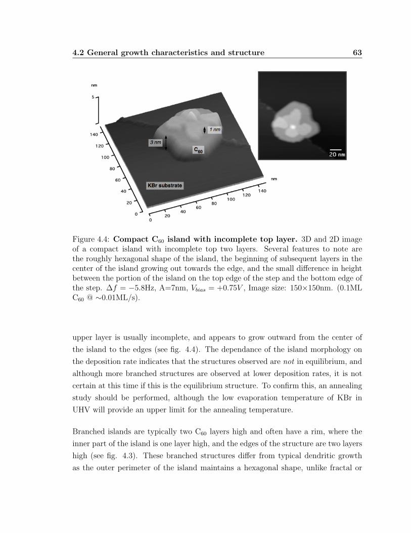
4.2 General growth characteristics and structure 63
Figure 4.4: Compact C60 island with incomplete top layer. 3D and 2D imageof a compact island with incomplete top two layers. Several features to note arethe roughly hexagonal shape of the island, the beginning of subsequent layers in thecenter of the island growing out towards the edge, and the small difference in heightbetween the portion of the island on the top edge of the step and the bottom edge ofthe step. ∆f = −5.8Hz, A=7nm, Vbias = +0.75V , Image size: 150×150nm. (0.1MLC60 @ ∼0.01ML/s).
upper layer is usually incomplete, and appears to grow outward from the center of
the island to the edges (see fig. 4.4). The dependance of the island morphology on
the deposition rate indicates that the structures observed are not in equilibrium, and
although more branched structures are observed at lower deposition rates, it is not
certain at this time if this is the equilibrium structure. To confirm this, an annealing
study should be performed, although the low evaporation temperature of KBr in
UHV will provide an upper limit for the annealing temperature.
Branched islands are typically two C60 layers high and often have a rim, where the
inner part of the island is one layer high, and the edges of the structure are two layers
high (see fig. 4.3). These branched structures differ from typical dendritic growth
as the outer perimeter of the island maintains a hexagonal shape, unlike fractal or
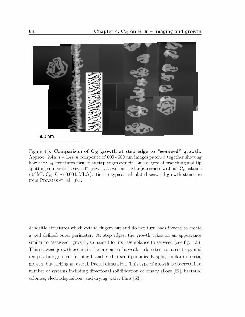
64 Chapter 4. C60 on KBr – imaging and growth
Figure 4.5: Comparison of C60 growth at step edge to “seaweed” growth.Approx. 2.4µm× 1.4µm composite of 600×600 nm images patched together showinghow the C60 structures formed at step edges exhibit some degree of branching and tipsplitting similar to “seaweed” growth, as well as the large terraces without C60 islands(0.2ML C60 @ ∼ 0.0045ML/s). (inset) typical calculated seaweed growth structurefrom Provatas et. al. [64].
dendritic structures which extend fingers out and do not turn back inward to create
a well defined outer perimeter. At step edges, the growth takes on an appearance
similar to “seaweed” growth, so named for its resemblance to seaweed (see fig. 4.5).
This seaweed growth occurs in the presence of a weak surface tension anisotropy and
temperature gradient forming branches that semi-periodically split, similar to fractal
growth, but lacking an overall fractal dimension. This type of growth is observed in a
number of systems including directional solidification of binary alloys [62], bacterial
colonies, electrodeposition, and drying water films [63].
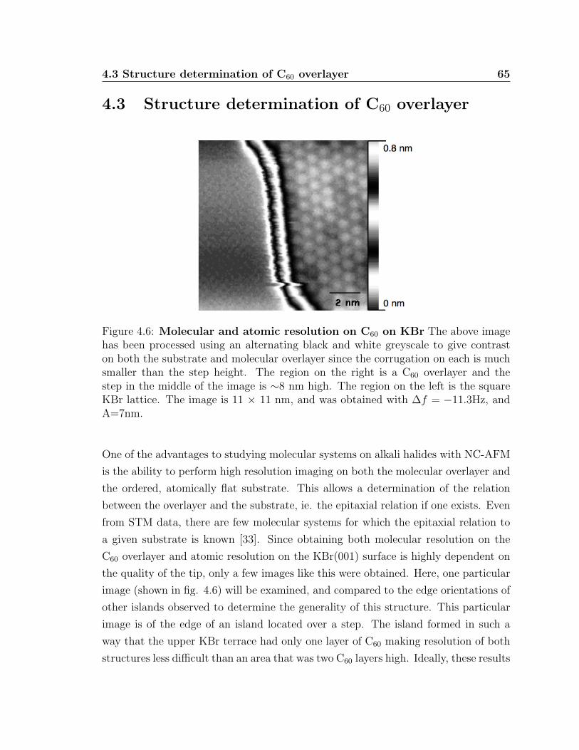
4.3 Structure determination of C60 overlayer 65
4.3 Structure determination of C60 overlayer
Figure 4.6: Molecular and atomic resolution on C60 on KBr The above imagehas been processed using an alternating black and white greyscale to give contraston both the substrate and molecular overlayer since the corrugation on each is muchsmaller than the step height. The region on the right is a C60 overlayer and thestep in the middle of the image is ∼8 nm high. The region on the left is the squareKBr lattice. The image is 11 × 11 nm, and was obtained with ∆f = −11.3Hz, andA=7nm.
One of the advantages to studying molecular systems on alkali halides with NC-AFM
is the ability to perform high resolution imaging on both the molecular overlayer and
the ordered, atomically flat substrate. This allows a determination of the relation
between the overlayer and the substrate, ie. the epitaxial relation if one exists. Even
from STM data, there are few molecular systems for which the epitaxial relation to
a given substrate is known [33]. Since obtaining both molecular resolution on the
C60 overlayer and atomic resolution on the KBr(001) surface is highly dependent on
the quality of the tip, only a few images like this were obtained. Here, one particular
image (shown in fig. 4.6) will be examined, and compared to the edge orientations of
other islands observed to determine the generality of this structure. This particular
image is of the edge of an island located over a step. The island formed in such a
way that the upper KBr terrace had only one layer of C60 making resolution of both
structures less difficult than an area that was two C60 layers high. Ideally, these results
66 Chapter 4. C60 on KBr – imaging and growth
would be compared with another technique for surface structure determination, for
example LEED. This was attempted but yielded inconclusive results (see appendix
B).
The first conclusion that can be drawn from both the large scale morphology pre-
viously discussed, and molecular resolution imaging, is that the C60 molecules form
a hexagonal arrangement on the KBr surface, despite the four-fold symmetry of the
substrate. This mismatch in symmetry is one of the factors which often leads to
coincident structures in molecular systems.
4.3.1 Structure determination from overlayer rotation angle
Recalling from chapter 1, the matrix elements describing the relation of the over-
layer lattice to the substrate can be determined from the lattice parameters of both
lattices, and the orientation of the overlayer with respect to the substrate lattice.
Measurements taken from a drift corrected version of the image in fig. 4.6 indicate
that there is only a small, if any, deformation of the C60 overlayer lattice, and an
alignment with the < 010 > direction of the KBr surface. Using the lattice parame-
ters for the conventional cell of KBr: a1 = a2 = 6.6 A, α = 90, and the equilibrium
lattice spacing of C60 : b1 = b2 = 10A, β = 60, and an overlayer rotation angle of:
θ = 30 corresponding to an alignment in the < 010 > direction, the matrix C is:
Ccalc =
[1.31 0.757
0 1.52
]'
[4/3 3/4
0 3/2
](4.1)
Since no column consists of integers, this structure is either coincidence-II or incom-
mensurate. Since the overlayer lattice may be slightly distorted from the values used,
it is possible that the matrix elements can be rounded to fractions.
Although atomic/molecular resolution was not achieved everywhere, it is possible to
extract information from large scale overview images about the number of rotational
domains. Three families of angles were found by measuring the relative orienta-
4.3 Structure determination of C60 overlayer 67
tions of the edges of the C60 islands found on terraces. The three hexagonal angles
(30, 60, 120), as well as the 90 angles are expected from the symmetry of the C60
and the KBr lattices respectively. However 20 and 80 angles were also measured
and most likely indicate two rotational domains 20 apart (note that 80 is the same
as an additional 20 rotation from 60). It should also be noted that neither of these
orientations correspond to the same < 010 > orientation observed in figure 4.6.
4.3.2 Structure determination by Image addition method
An image clearly displaying both the substrate and overlayer lattice, in principle,
contains all of the information needed to determine the structure in that area, ie. the
lattice parameters of each lattice and the relative orientation of the overlayer to the
substrate. Similar to overlaying the two lattices on transparencies, addition of the
two lattice images by computer software can be used to look for points where the
two lattices overlap in the same way. If these points repeat in a periodic fashion, a
supercell can be defined.
From a molecular/atomic resolution image, an equally sized section of the substrate
and the overlayer is cut out. An averaged unit cell image of the same size is created by
averaging over all unit cells (as defined by a selected area) in the image, and re-tiling
the unit cell (see fig. 4.7). This unit cell averaging reduces noise on the image, allows
re-tiling of a larger area than perhaps is clear in the original image, and if defined
correctly, improves the accuracy of the lattice spacing. The averaged unit cell images
are then added:
(KBrAvgUnitCell + C60AvgUnitCell)× 0.5 = CombinedImage (4.2)
The result is a combined image that represents the relationship between the overlayer
and the substrate. The combined image is used to look for any features which may
repeat. An irregular diamond shape is outlined in the combined image in figure 4.7
which was used to visually identify periodicities. Any periodicity in this image will
68 Chapter 4. C60 on KBr – imaging and growth
represent a periodicity in the overlayer–substrate geometry, and will thus define a
supercell.
To test for the correct choice of a supercell, the supercell is cut out and re-tiled,
without rotation or mirror operations, to recreate the combined image. The difference
of the two images is then taken compare the choice of supercell:
(CombinedImage−RetiledImage)× 0.5 + 128 = DifferenceImage (4.3)
If the difference image is featureless (at a grey-scale level of 128) the re-tiled image
is identical to the original combined image. (Note: A Moire pattern may appear if
some of the supercells are not placed exactly during retiling. Striking features will
appear if the wrong unit cell is chosen, including a large amplitude Moire pattern
and/or pieces of the combined image showing through.)
Using this method, two different supercells were identified, shown in fig. 4.8, with
respect to the KBr lattice. The first can be defined with respect to the conventional
cell of the KBr lattice in matrix notation as:
C1 =
[11/8 3/4
0 3/2
](4.4)
This corresponds to the primative cell of the c11×3 structure, as it would be defined
in Wood’s notation.
The second supercell can be defined with respect to the conventional cell of the KBr
lattice as well. In Wood’s notation this is an 8× 3 superstructure, or with respect to
the primitive cell of the KBr, a√
8 ×√
3R30. Or in matrix notation, with respect
to the KBr conventional cell:
C2 =
[4/3 3/4
0 3/2
](4.5)
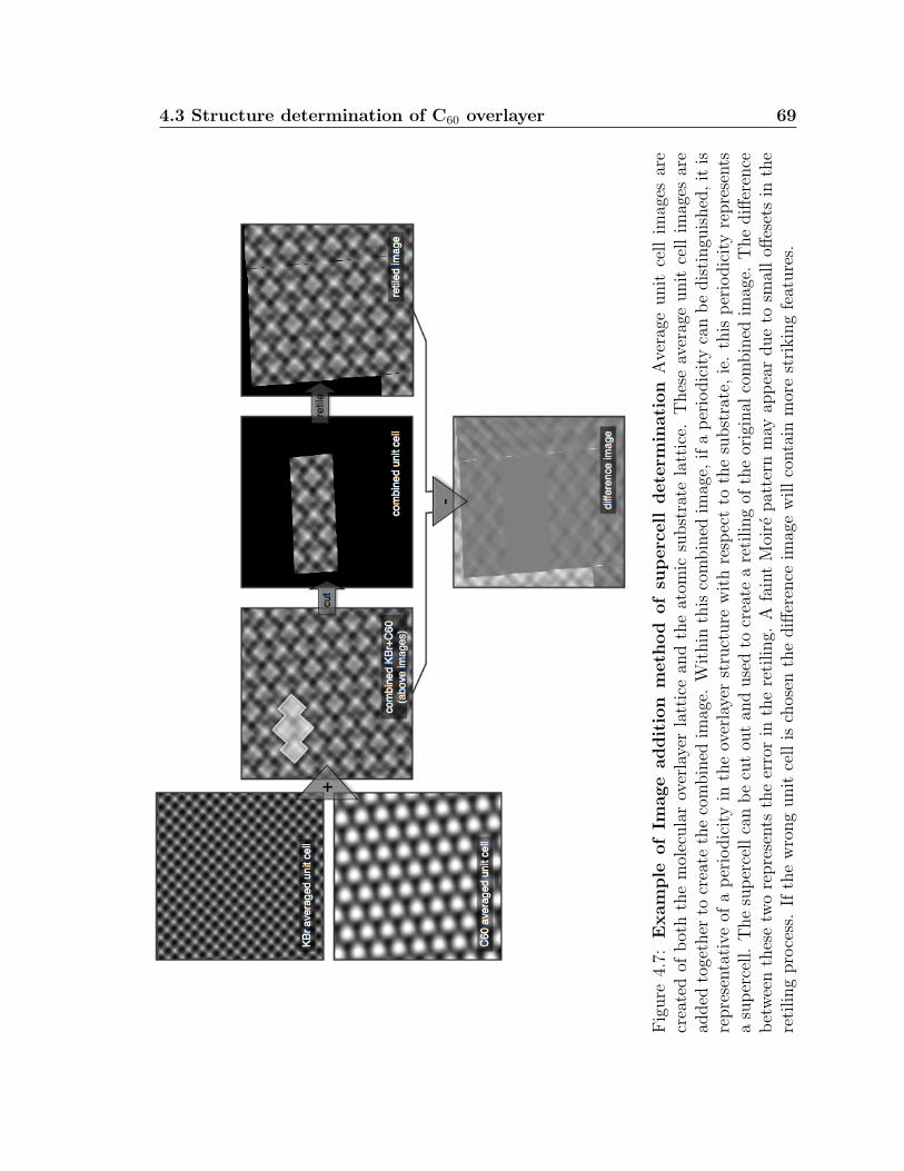
4.3 Structure determination of C60 overlayer 69
Fig
ure
4.7:
Exam
ple
of
Image
additio
nm
eth
od
of
superc
ell
dete
rmin
ation
Ave
rage
unit
cell
imag
esar
ecr
eate
dof
bot
hth
em
olec
ula
rov
erla
yer
latt
ice
and
the
atom
icsu
bst
rate
latt
ice.
Thes
eav
erag
eunit
cell
imag
esar
ead
ded
toge
ther
tocr
eate
the
com
bin
edim
age.
Wit
hin
this
com
bin
edim
age,
ifa
per
iodic
ity
can
be
dis
tingu
ished
,it
isre
pre
senta
tive
ofa
per
iodic
ity
inth
eov
erla
yer
stru
cture
with
resp
ect
toth
esu
bst
rate
,ie
.th
isper
iodic
ity
repre
sents
asu
per
cell.
The
super
cell
can
be
cut
out
and
use
dto
crea
tea
reti
ling
ofth
eor
igin
alco
mbin
edim
age.
The
diff
eren
cebet
wee
nth
ese
two
repre
sents
the
erro
rin
the
reti
ling.
Afa
int
Moi
repat
tern
may
appea
rdue
tosm
alloff
eset
sin
the
reti
ling
pro
cess
.If
the
wro
ng
unit
cell
isch
osen
the
diff
eren
ceim
age
willco
nta
inm
ore
strikin
gfe
ature
s.
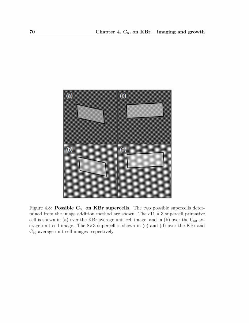
70 Chapter 4. C60 on KBr – imaging and growth
Figure 4.8: Possible C60 on KBr supercells. The two possible supercells deter-mined from the image addition method are shown. The c11 × 3 supercell primativecell is shown in (a) over the KBr average unit cell image, and in (b) over the C60 av-erage unit cell image. The 8×3 supercell is shown in (c) and (d) over the KBr andC60 average unit cell images respectively.
4.3 Structure determination of C60 overlayer 71
This unit cell, defined in matrix notation agrees well with the structure predicted
from the lattice constants and overlayer rotation determined from the image (see
eqn. 4.1). Although the first supercell identified has a smaller primitive cell, the
8 × 3 both agrees better with the calculated matrix, as well as appearing to be a
slightly better fit to the C60 lattice. However, both will be considered as the size of
the C60 molecules makes a precise determination of their location difficult.
Both of these structures fit the description of a coincidence-II structure as all of the
matrix elements are rational, but no column of the matrix consists of integers. Hence,
a supercell can be constructed and there is a distinct registry and phase coherence
between the two lattices, though only some of the overlayer lattice points lie on lattice
lines of the substrate. The presence of a coincidence-II structure also implies that
the cost of deforming the overlayer is greater than the energetic gain of finding an
phase coherent registry with the lattice. A prediction algorithm, outlined by Hillier
et al. [65], and described in appendix C was used to search for commensurate and
coincidence-I structures. As no structures were found within a reasonable range of
C60 lattice constants, it will be assumed that any possible C60 structures will be
either coincidence-II or incommensurate. In this case, the lack of available lattice
geometries will be the primary reason for the coincidence-II structures. However, the
presence of these out-of-phase structures still suggests that the cost of deforming the
overlayer to an in-phase configuration is greater than the energetic gain of forming
a structure which satisfies the overlayer–substrate interaction. This implies that the
C60 –C60 intralayer interaction is stronger than the C60 –KBr interaction, which is
also consistent with the observation of an island growth mode.
The image addition method described here is a relatively simple way of determining
structures. It does however have some limitations as multiple unit cells may be
apparent if the difference between them is small and/or the positions of the lattice
points are ill-defined due to a significant extent of the atom or molecule. The major
advantage to this method, besides its simplicity, is that two parts of the same image
are compared such that any drift and/or non-linearities in the piezos are automatically
excluded and drift correction is not needed.

72 Chapter 4. C60 on KBr – imaging and growth
Figure 4.9: Model structures from image overlay. Model shown above createdby overlaying circles on lattice identified in molecular resolution image. The twosupercells identified by the image addition method can be identified here also. (a)primitive cell of c11× 3 and (b) 8× 3.
4.3.3 Model structures from image overlay and reconstruc-
tion
A model of the C60 on KBr structures was created by overlaying a lattice of circles on
the original molecular resolution image (see fig. 4.9). The two unit cells identified by
the image addition method can also be identified in the model structure (fig. 4.9a,b).
However, the slight shifts in position of the molecules defining the supercells in figure
4.9a,b may be due to errors in re-creating the lattice structure. Thus it should not
be taken as an indication that these supercells are invalid. Rather, this method is
more useful in determining the translational position of the overlayer molecules with
respect to the KBr, and as a first look at the symmetry of the supercells.
From the information provided by the image overlay, a model of the structure seen
in the molecular resolution image can be reproduced (see fig. 4.10). For either of the
proposed structures the C60 molecules sit on alternating top sites, ie. top K+ then
top Br−, in the < 010 > direction for some rows. The number of out of phase and
symmetry equivalent molecules depends on the exact structure, and this cannot be
well determined from the image overlay method.
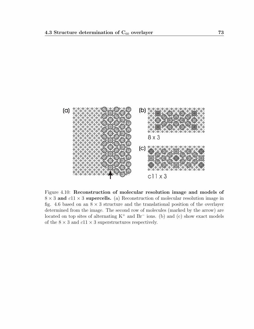
4.3 Structure determination of C60 overlayer 73
Figure 4.10: Reconstruction of molecular resolution image and models of8× 3 and c11× 3 supercells. (a) Reconstruction of molecular resolution image infig. 4.6 based on an 8 × 3 structure and the translational position of the overlayerdetermined from the image. The second row of molecules (marked by the arrow) arelocated on top sites of alternating K+ and Br− ions. (b) and (c) show exact modelsof the 8× 3 and c11× 3 superstructures respectively.
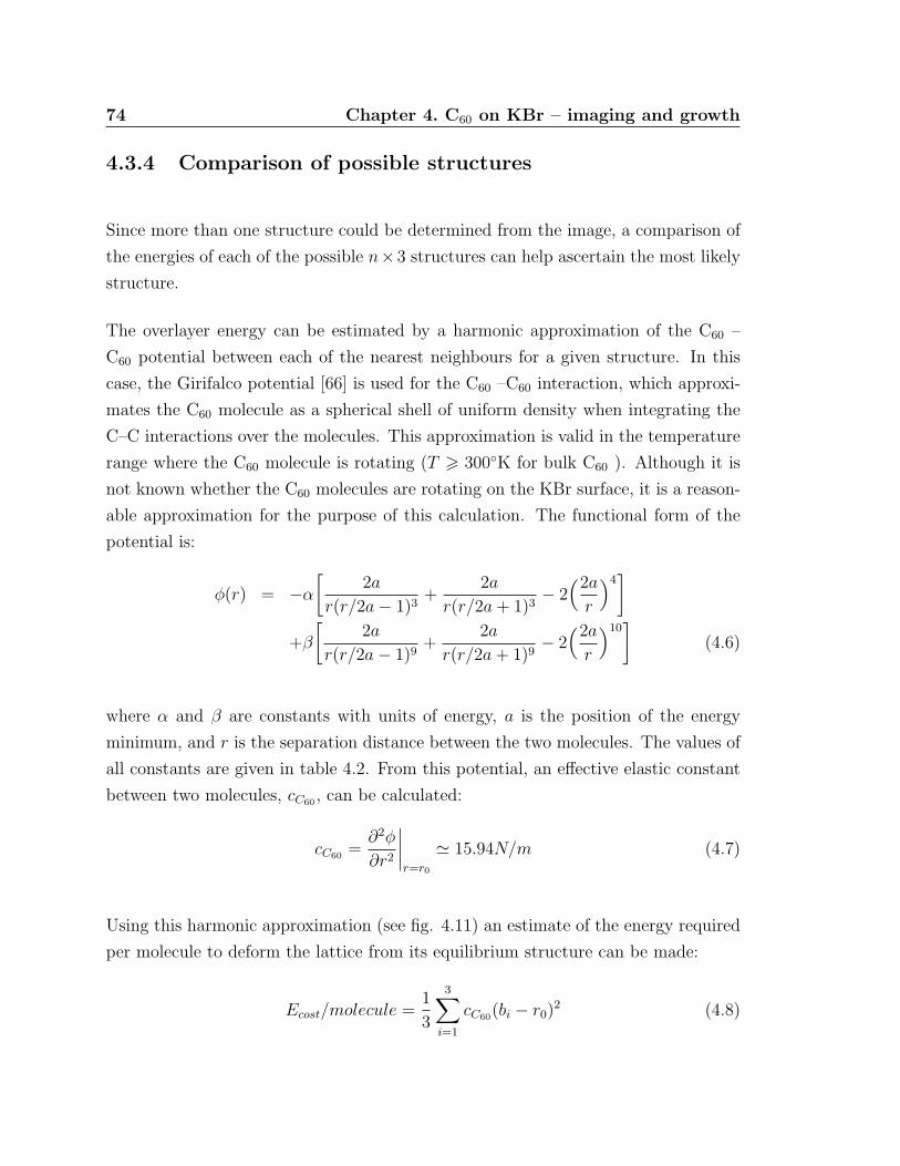
74 Chapter 4. C60 on KBr – imaging and growth
4.3.4 Comparison of possible structures
Since more than one structure could be determined from the image, a comparison of
the energies of each of the possible n×3 structures can help ascertain the most likely
structure.
The overlayer energy can be estimated by a harmonic approximation of the C60 –
C60 potential between each of the nearest neighbours for a given structure. In this
case, the Girifalco potential [66] is used for the C60 –C60 interaction, which approxi-
mates the C60 molecule as a spherical shell of uniform density when integrating the
C–C interactions over the molecules. This approximation is valid in the temperature
range where the C60 molecule is rotating (T > 300K for bulk C60 ). Although it is
not known whether the C60 molecules are rotating on the KBr surface, it is a reason-
able approximation for the purpose of this calculation. The functional form of the
potential is:
φ(r) = −α
[2a
r(r/2a− 1)3+
2a
r(r/2a + 1)3− 2
(2a
r
)4]
+β
[2a
r(r/2a− 1)9+
2a
r(r/2a + 1)9− 2
(2a
r
)10]
(4.6)
where α and β are constants with units of energy, a is the position of the energy
minimum, and r is the separation distance between the two molecules. The values of
all constants are given in table 4.2. From this potential, an effective elastic constant
between two molecules, cC60 , can be calculated:
cC60 =∂2φ
∂r2
∣∣∣∣r=r0
' 15.94N/m (4.7)
Using this harmonic approximation (see fig. 4.11) an estimate of the energy required
per molecule to deform the lattice from its equilibrium structure can be made:
Ecost/molecule =1
3
3∑i=1
cC60(bi − r0)2 (4.8)

4.3 Structure determination of C60 overlayer 75
Binding Energy 1.4 eV [38]
Equilibrium separation (r0) 10.06 A[66]
α 74.94× 10⁻²²J [66]β 135.95× 10⁻²⁵J [66]
2a 7.1 A[66]
Table 4.2: C60 parameters for Girifalco potential and energy calculation
where the bi are the deformed lattice constants in each direction, r0 is the equilib-
rium separation between molecules, i runs from 1 to 3 summing the energies for
each uniquely displaced nearest neighbour, and the factor of 1/3 reduces the en-
ergy to be comparable to the binding energy between two molecules, ie. the energy
cost/molecule.
A relative estimate of the interface energy can also be obtained by determining the
ratio of “out of phase” to the total number of molecules. These “out of phase”
molecules, which do not sit on lattice points, will have some increased energy com-
pared to molecules which do sit on lattice points. Although each “out of phase”
molecule will have a different contribution to the total interface energy depending on
the exact position of the molecule with respect to the substrate potential, this ratio
can give a rough estimate of the relative energies.
A number of possible structures were determined by looking at the equilibrium lattice
of the C60 molecules overlaid on the KBr(001) lattice. Structures which visually
appeared to be a close fit were considered. The overlayer lattice constants to make
each structure conform to the KBr lattice were calculated and used to determine
the energy cost per molecule for each. The ratio of “out of phase” to total number
of molecules was also calculated for each structure. The results are tabulated in
table 4.3. It should be noted that the harmonic approximation will underestimate
the energy required for compression of the lattice, and overestimate the energy for
expansion of the lattice. From the relative energies as well as the image addition
method, the 8 × 3 overlayer structure seems the most probable structure for this
area.
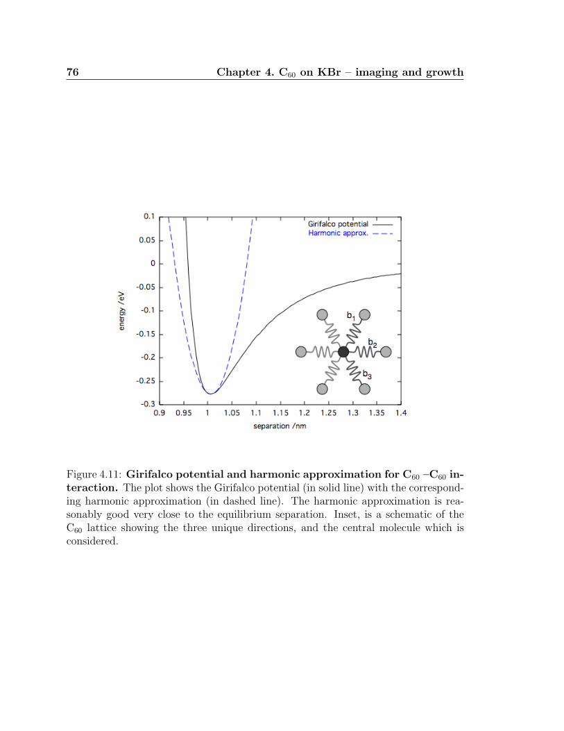
76 Chapter 4. C60 on KBr – imaging and growth
Figure 4.11: Girifalco potential and harmonic approximation for C60 –C60 in-teraction. The plot shows the Girifalco potential (in solid line) with the correspond-ing harmonic approximation (in dashed line). The harmonic approximation is rea-sonably good very close to the equilibrium separation. Inset, is a schematic of theC60 lattice showing the three unique directions, and the central molecule which isconsidered.
4.3 Structure determination of C60 overlayer 77
Structure Lattice Parameters Ecost#out−of−phase
total#molec
c5× 3 b1=9.62A 0.068 eV 0.75b2=9.90Aβ = 59.0
8× 3 b1=10.10A 0.005 eV 0.92b2=9.90Aβ = 60.7
c11× 3 b1=10.34A 0.030 eV 0.88b2=9.90Aβ = 61.4
13× 3 b1=9.90A 0.012 eV 0.95b2=9.90Aβ = 60.0
18× 3 b1=9.82A 0.023 eV 0.96b2=9.90Aβ = 59.73
c21× 3 b1=9.98A 0.017 eV 0.94b2=9.90Aβ = 60.3
Table 4.3: Comparison of different possible n× 3 C60 overlayer structures

78 Chapter 4. C60 on KBr – imaging and growth
Figure 4.12: First layer bright and dim C60 molecules Image in (a) shows thefirst layer of a C60 island with molecular resolution. Image size: 20 nm × 20 nm,∆f = −11.3Hz, A=7 nm. The line in (a) is represented in cross-section in (b)with the height difference of ∼20 pm indicated by the arrow, and dashed lines. Themolecular models in (c) show a small height difference between a C60 molecule witha pentagonal face in contact with the surface (left) and a hexagonal face in contactwith the surface (right).
4.4 First layer C60 – Bright and dim molecules
Molecular resolution of the first layer of C60 revealed two different effective heights in
the AFM topography (see fig. 4.12a), giving the appearance of “bright” and “dim”
molecules. Measurement of the height difference between these “bright” and “dim”
molecules yielded a value of 21 ± 3 pm (see fig. 4.12b). It should be noted that
the ability of the instrument to measure height difference and corrugations on the
order of 10’s of pm indicates that the instrument is very stable, and the electronics
contribute very little noise to the measurement.
The geometrical height difference between two different orientations of the C60 molecule,
namely the five-fold ring, and the three-fold ring in contact with the surface (see fig.
4.12c), can be calculated. The expressions for the center to centroid distances for
both the pentagonal and hexagonal faces of a truncated icosahedron, based on an
icosahedron of edge length a = 1, are respectively given by [67]:
4.4 First layer C60 – Bright and dim molecules 79
r5 =1
2
√1
10(125 + 41
√41) (4.9)
r6 =1
2
√3
2(7 + 3
√5) (4.10)
The ratio of the height difference to the taller of the two orientations can be used to
give an estimate of the height difference that would be observed in the AFM image:
∆ho =|r5 − r6|
r5
× ho (4.11)
where ho is the height of the taller species measured in the image, and ∆ho is then
the expected height difference. This geometrical height difference was found to be
21.7 pm, which is in very good agreement with the measured height difference. The
close correspondence of the apparent height difference in the AFM topography to the
geometrical height difference between these two orientations indicates that this is a
likely origin of the observed “bright/dim” phenomenon.
Additionally, the “bright” and “dim” molecules were not observed to change contrast
(ie. from “bright” to “dim” or vice-versa) on a time scale of > 30 minutes, indicating
under this interpretation that the molecules are not rotating out of the plane of the
substrate in the first layer on KBr at room temperature. Sub-molecular resolution
imaging of the C60 molecules would show whether or not there is an in-plane rotation,
and hopefully confirm the proposed orientations for both the “bright” and “dim”
molecules. This has not yet been achieved, but may be possible at low temperature.
Also, the lack of rotation implies a strong interaction either between the C60 molecules
or between the molecules and the substrate. However, the growth and structure of
C60 on KBr has indicated a weak interaction between the molecule and the substrate.
One possible explanation for this is that the molecules are sterically hindered from
this rotation due to the slight deformation of the lattice as discussed in the previous
section.
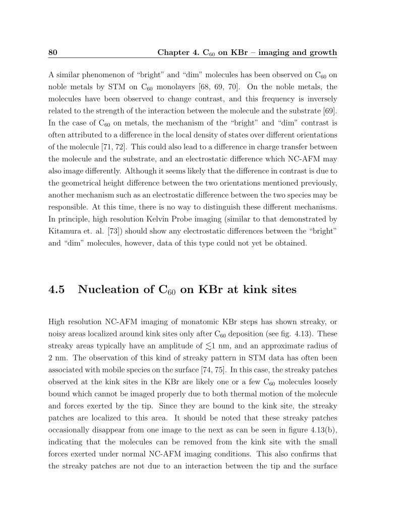
80 Chapter 4. C60 on KBr – imaging and growth
A similar phenomenon of “bright” and “dim” molecules has been observed on C60 on
noble metals by STM on C60 monolayers [68, 69, 70]. On the noble metals, the
molecules have been observed to change contrast, and this frequency is inversely
related to the strength of the interaction between the molecule and the substrate [69].
In the case of C60 on metals, the mechanism of the “bright” and “dim” contrast is
often attributed to a difference in the local density of states over different orientations
of the molecule [71, 72]. This could also lead to a difference in charge transfer between
the molecule and the substrate, and an electrostatic difference which NC-AFM may
also image differently. Although it seems likely that the difference in contrast is due to
the geometrical height difference between the two orientations mentioned previously,
another mechanism such as an electrostatic difference between the two species may be
responsible. At this time, there is no way to distinguish these different mechanisms.
In principle, high resolution Kelvin Probe imaging (similar to that demonstrated by
Kitamura et. al. [73]) should show any electrostatic differences between the “bright”
and “dim” molecules, however, data of this type could not yet be obtained.
4.5 Nucleation of C60 on KBr at kink sites
High resolution NC-AFM imaging of monatomic KBr steps has shown streaky, or
noisy areas localized around kink sites only after C60 deposition (see fig. 4.13). These
streaky areas typically have an amplitude of .1 nm, and an approximate radius of
2 nm. The observation of this kind of streaky pattern in STM data has often been
associated with mobile species on the surface [74, 75]. In this case, the streaky patches
observed at the kink sites in the KBr are likely one or a few C60 molecules loosely
bound which cannot be imaged properly due to both thermal motion of the molecule
and forces exerted by the tip. Since they are bound to the kink site, the streaky
patches are localized to this area. It should be noted that these streaky patches
occasionally disappear from one image to the next as can be seen in figure 4.13(b),
indicating that the molecules can be removed from the kink site with the small
forces exerted under normal NC-AFM imaging conditions. This also confirms that
the streaky patches are not due to an interaction between the tip and the surface
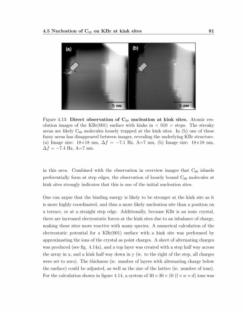
4.5 Nucleation of C60 on KBr at kink sites 81
Figure 4.13: Direct observation of C60 nucleation at kink sites. Atomic res-olution images of the KBr(001) surface with kinks in < 010 > steps. The streakyareas are likely C60 molecules loosely trapped at the kink sites. In (b) one of thesefuzzy areas has disappeared between images, revealing the underlying KBr structure.(a) Image size: 18×18 nm, ∆f = −7.1 Hz, A=7 nm, (b) Image size: 18×18 nm,∆f = −7.4 Hz, A=7 nm.
in this area. Combined with the observation in overview images that C60 islands
preferentially form at step edges, the observation of loosely bound C60 molecules at
kink sites strongly indicates that this is one of the initial nucleation sites.
One can argue that the binding energy is likely to be stronger at the kink site as it
is more highly coordinated, and thus a more likely nucleation site than a position on
a terrace, or at a straight step edge. Additionally, because KBr is an ionic crystal,
there are increased electrostatic forces at the kink sites due to an inbalance of charge,
making these sites more reactive with many species. A numerical calculation of the
electrostatic potential for a KBr(001) surface with a kink site was performed by
approximating the ions of the crystal as point charges. A sheet of alternating charges
was produced (see fig. 4.14a), and a top layer was created with a step half way across
the array in x, and a kink half way down in y (ie. to the right of the step, all charges
were set to zero). The thickness (ie. number of layers with alternating charge below
the surface) could be adjusted, as well as the size of the lattice (ie. number of ions).
For the calculation shown in figure 4.14, a system of 30× 30× 10 (l×w×d) ions was
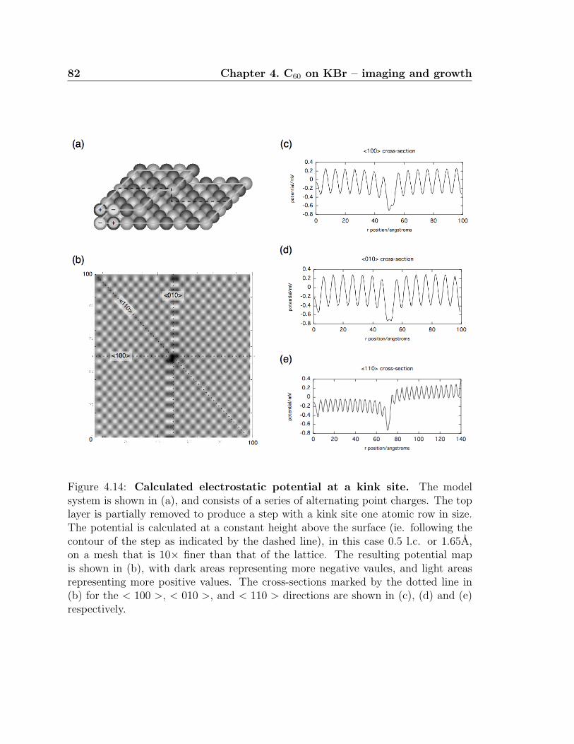
82 Chapter 4. C60 on KBr – imaging and growth
Figure 4.14: Calculated electrostatic potential at a kink site. The modelsystem is shown in (a), and consists of a series of alternating point charges. The toplayer is partially removed to produce a step with a kink site one atomic row in size.The potential is calculated at a constant height above the surface (ie. following thecontour of the step as indicated by the dashed line), in this case 0.5 l.c. or 1.65A,on a mesh that is 10× finer than that of the lattice. The resulting potential mapis shown in (b), with dark areas representing more negative vaules, and light areasrepresenting more positive values. The cross-sections marked by the dotted line in(b) for the < 100 >, < 010 >, and < 110 > directions are shown in (c), (d) and (e)respectively.
4.5 Nucleation of C60 on KBr at kink sites 83
used. The potential was then calculated on a mesh finer than the lattice at a constant
height above the surface (see dashed line in fig. 4.14a) by summing the contribution
from all charges at each point [76]:
V (r) =1
4πε0
N∑i=1
N∑j=1
M∑k=1
qijk√(x− xi)2 + (y − yj)2 + (z0 − zk)
(4.12)
where i, j, k are the indices of the summation corresponding to the positions of the
charges, the lattice is a size N×N×M , the qijk are the charges at the given positions,
xi, yj, and zk are the coordinates of the charge, x and y correspond to the position
on the mesh where the potential is calculated, and z0 is the constant height above
the surface where the potential is calculated. The 2D result of the potential at a
constant height of 0.5 l.c. is shown in figure 4.14b. As the primary mechanism for
atomic resolution on alkali halides is suggested to be due to electrostatics [27], it is
perhaps interesting to note that the general features of the electrostatic potential
correspond quite closely to atomic resolution images of similar structures (refer back
to fig. 3.1).
The calculated potential shows a minimum (or a maximum depending on the sign
of the charges) at the kink site. This can be seen in center of figure 4.14b, as well
as in each of the cross-sections (fig. 4.14c,d,e) passing through the kink site. The
minimum extends ∼0.4 mV below the minima located over the negatively charged
ions.
Although the C60 molecule is not polar, its relatively large polarizability [77] indicates
that it will be attracted to this minimum (or maximum) in the electrostatic potential
through an induced dipole in the molecule. The depth of the attractive potential due
to this induced dipole can be estimated using the polarizability. Assuming a perfect
dipole [76]:
U = −~p · ~E (4.13)
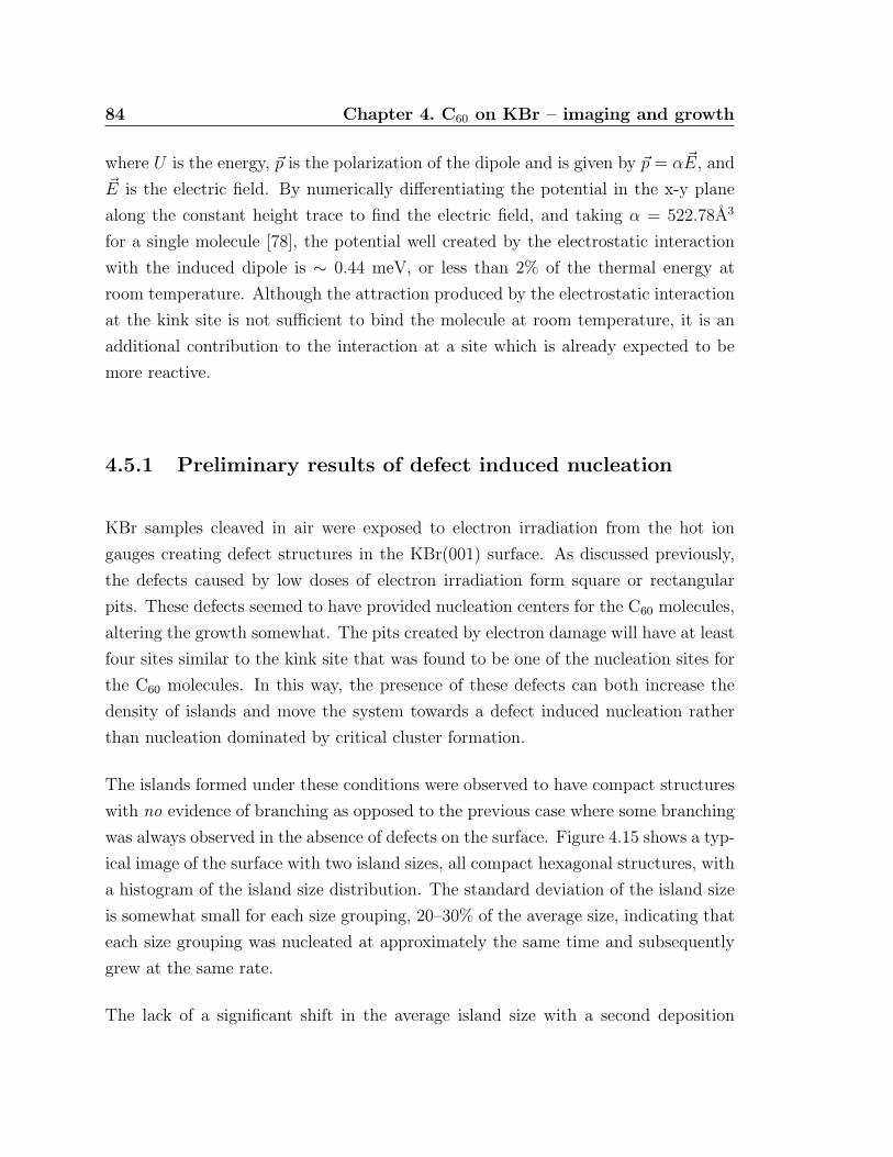
84 Chapter 4. C60 on KBr – imaging and growth
where U is the energy, ~p is the polarization of the dipole and is given by ~p = α~E, and~E is the electric field. By numerically differentiating the potential in the x-y plane
along the constant height trace to find the electric field, and taking α = 522.78A3
for a single molecule [78], the potential well created by the electrostatic interaction
with the induced dipole is ∼ 0.44 meV, or less than 2% of the thermal energy at
room temperature. Although the attraction produced by the electrostatic interaction
at the kink site is not sufficient to bind the molecule at room temperature, it is an
additional contribution to the interaction at a site which is already expected to be
more reactive.
4.5.1 Preliminary results of defect induced nucleation
KBr samples cleaved in air were exposed to electron irradiation from the hot ion
gauges creating defect structures in the KBr(001) surface. As discussed previously,
the defects caused by low doses of electron irradiation form square or rectangular
pits. These defects seemed to have provided nucleation centers for the C60 molecules,
altering the growth somewhat. The pits created by electron damage will have at least
four sites similar to the kink site that was found to be one of the nucleation sites for
the C60 molecules. In this way, the presence of these defects can both increase the
density of islands and move the system towards a defect induced nucleation rather
than nucleation dominated by critical cluster formation.
The islands formed under these conditions were observed to have compact structures
with no evidence of branching as opposed to the previous case where some branching
was always observed in the absence of defects on the surface. Figure 4.15 shows a typ-
ical image of the surface with two island sizes, all compact hexagonal structures, with
a histogram of the island size distribution. The standard deviation of the island size
is somewhat small for each size grouping, 20–30% of the average size, indicating that
each size grouping was nucleated at approximately the same time and subsequently
grew at the same rate.
The lack of a significant shift in the average island size with a second deposition
4.5 Nucleation of C60 on KBr at kink sites 85
Figure 4.15: Island sizes of C60 on KBr surface with defects. (a) Imageof compact islands of two sizes on KBr with defects. Image size: 650 × 650nm,∆f = −5.8Hz, A=7nm. (b) Histogram of island radii for initial deposition (solidline) and second deposition (long dash line). Calculated average value and standarddeviation from first deposition used to plot gaussians for large and small islands toguide the eye. Inset is a plot from Sagui and Grant [31] of the time evolution of 2Dgrowth for zero nucleation rate width, ie. uniform nucleation rate.

86 Chapter 4. C60 on KBr – imaging and growth
(equivalent to longer time), as well as the slight shoulder on the left-hand side of
the small size island distribution, compares well with the steady-state homogeneous
nucleation theory result for a constant nucleation rate with a narrow, or zero-extent
(δ-function) distribution [31]. In the case of defect induced nucleation one might
expect the critical nucleus size, and thus the nucleation rate width, to approach zero,
ie. a single molecule bound to a defect can nucleate island growth. As the nucleation
rate distribution width is related to the critical nucleus size, and thus temperature,
the behaviour of these distributions as a function of the substrate temperature should
confirm whether this is defect induced nucleation.
The two sizes of islands, one with an average diameter of 26.6 nm, and the other with
an average diameter of 109 nm for this sample, may be caused by two different types of
defects, or a combination of defect induced nucleation and critical cluster formation.
In the possible case of two different types of defects, one may have a longer ranging
interaction, for example a net electrostatic charge, resulting in an attractive potential
well around the defect, and thus a greater probability of collecting a larger number of
molecules. This difference in range of forces from a defect seems quite likely, especially
considering atomic resolution of defects formed by electron irradiation showed two
types of defects, one with a halo and one without (see fig. 3.2). The observation of
a halo in NC-AFM indicates the presence of such a long range interaction.
The ability to create defects using electron bombardment and subsequently deposit
molecules which have a preferred nucleation site at these defects presents an inter-
esting way to direct growth. In principle, the growth of molecules could be directed
by using a focused electron beam to produce localized defects. The facility to direct
growth in this way could be quite useful in developing molecular electronics devices.
4.6 Kelvin Probe imaging of C60 on KBr 87
4.6 Preliminary results with Kelvin Probe imag-
ing of C60 on KBr
Kelvin Probe imaging was used to measure the difference in electrostatics between
the C60 molecules and the insulating KBr substrate. Frequency shift vs. voltage
curves were performed on both the C60 islands as well as the neighbouring substrate.
The minima in the parabolic ∆f vs. V measurements showed a consistent trend for
the contact potential difference of the C60 molecules to be larger than the contact
potential for the KBr substrate. However, the difference between the two CPD values
was not found to be consistent, typically varying from ∼ 0.07 − 0.3V from sample
to sample, and sometimes even measurement to measurement. Likely due to this
variability in the CPD difference, kelvin probe measurements on pure C60 on KBr
samples often were unsuccessful, or of poor quality.
Kelvin probe images were obtained after gold was deposited on the surface (see fig.
4.16a,b), with a contrast of ∼ 1V , corresponding well to frequency shift vs. voltage
measurements on the same sample. This difference in the CPD is larger than that
measured on samples without gold clusters, which likely contributed to the improved
kelvin probe contrast. One possible explanation for the larger CPD contrast observed
on the sample with gold is a shift in the work function of the C60 molecules resulting
from a charge transfer between the molecules and the deposited gold atoms.
The successful application of Kelvin probe microscopy to this and other heterogeneous
systems would be useful for chemical species differentiation. Since the material of
the tip is often uncertain, as interactions with the sample can often cause material to
move to or from the tip, chemical identification using this technique would be difficult.
However, as can be seen from figure 4.16b, the area covered by C60 molecules can
be clearly distinguished from the KBr substrate. This could become increasingly
important as systems with larger numbers of components are used. However, further
understanding of the contrast mechanism for kelvin probe on an insulating substrate
is needed, as well as further experimentation to understand the effect of the added
metal atoms on the CPD contrast.
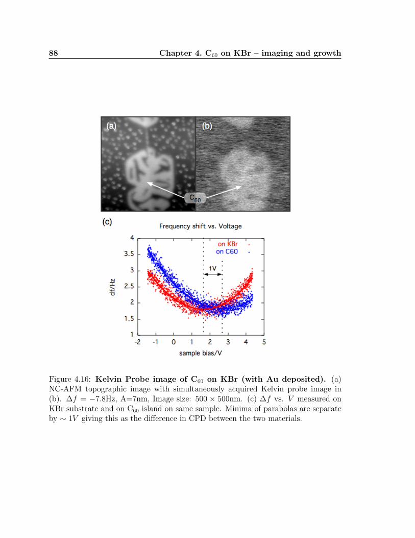
88 Chapter 4. C60 on KBr – imaging and growth
Figure 4.16: Kelvin Probe image of C60 on KBr (with Au deposited). (a)NC-AFM topographic image with simultaneously acquired Kelvin probe image in(b). ∆f = −7.8Hz, A=7nm, Image size: 500 × 500nm. (c) ∆f vs. V measured onKBr substrate and on C60 island on same sample. Minima of parabolas are separateby ∼ 1V giving this as the difference in CPD between the two materials.
Chapter 5
Conclusions and Outlook
As the NC-AFM technique is applied to wider range of problems in surface science, it
is becoming increasingly clear that NC-AFM has the potential to add to the field of
surface science on insulators in a similar way as STM was able to provide for surface
science on conducting substrates. The non-destructive, high-resolution imaging that
both tools are capable of allows investigation of the nucleation and growth processes
and structure of deposited materials. As the growth and structure of the deposited
material depend on a careful interplay of interactions between the substrate and
overlayer, especially in molecular systems, there is a wealth of physical information
that can be obtained about the driving forces and relative energetics dominating
these processes. The results presented here are an initial step towards uncovering
these physical processes. Further experimental work on different combinations of
molecules and insulating substrates will be needed to make generalized statements
about the interactions between molecules and insulators.
The imaging capabilities of the JEOL SPM system were tested in a variety of modes
including atomic scale imaging with the AFM. The sample preparation instruments
were used to prepare clean insulating substrate surfaces on which to study the growth
of molecules. The KBr(001) surface was characterized using LEED, contact mode
AFM, and NC-AFM. Atomic resolution of the KBr surface was obtained for both
air-cleaved and UHV-cleaved samples. Atomic stick-slip was also imaged in LF-AFM
90 Chapter 5. Conclusions and Outlook
mode at variable temperature leading to the possibility of studying temperature de-
pendance of friction effects as well as measuring forces involved in molecular manip-
ulation.
The growth of C60 on KBr was studied, revealing an island growth mode of both
branched and compact structures. An epitaxial relation for the C60 overlayer was
determined to be an 8 × 3 supercell for one area. This appears not to be a general
structure as the orientation of crystallites not formed on KBr steps have a differ-
ent edge orientation. However, from calculations performed, all epitaxial structures
within a reasonable range of overlayer deformations are of the type coincidence-II.
Thus the presence of any of these structures indicates that the cost of deforming the
overlayer lattice is larger than the energetic gain of forming a more phase-coherent
registry with the substrate lattice. This implies, as does the island growth mode
observed, that the C60 intralayer interaction is stronger than the C60 -substrate in-
teraction for the KBr(001) surface. To confirm this, ab initio calculation should be
performed to determine the strength and stiffness of the C60 -KBr interaction poten-
tial to then compare to the C60 -C60 interaction. Additionally, theoretical work on
the growth mechanisms will be required to understand more thoroughly the driving
forces behind the unusual, branched structures observed in the C60 on KBr system.
The kink sites in the KBr steps were identified as one of the initial nucleation sites of
the C60 molecules through NC-AFM imaging. A calculation of the electrostatics of
this type of surface morphology indicated that there was a small, but additional con-
tribution to the binding potential through the polarization of the C60 molecule at the
kink site. Although this is not a significant effect for the non-polar C60 molecule, it
may be significant for molecules with permanent electrostatic moments. The prelim-
inary work performed on the modification of surfaces indicates that the SEM could
be used to produce ESD-type defects on the KBr surface. Growth of C60 on sur-
faces with these kinds of defects show that the growth is modified by the presence
of defects. In future, the SEM may be used to create localized defects to steer the
growth to areas where molecules are desired, for example between deposited elec-
trodes. High resolution images of monolayer areas of C60 revealed an apparent height
difference of 21± 3 pm between some molecules. This height difference corresponds
very closely to the geometrical height difference of the C60 molecule in two different

91
orientations, namely with the hexagonal ring and the pentagonal ring in contact with
the substrate. Kelvin probe imaging of the C60 structures on KBr was attempted with
limited success, though in principle it could be used as a method of distinguishing
different species on samples of this kind.
Greater understanding of the interactions between molecules and insulating surfaces
will be crucial to the future design and implementation of a planar single molecule
electronic device. Without this information, the engineering of such a device would
be left to trial and error, and understanding its behaviour would be difficult. From
the device engineering perspective, the C60 on KBr system seems less than ideal
as the deposited material forms widely spaced clusters containing many molecules.
There are two main solutions to this problem. Subtractive manipulation should
be possible with an AFM tip, whereby molecules are removed from an electrically
contacted cluster by a physical probe. It has recently been shown that semiconductor
atoms can be manipulated by NC-AFM [79, 80] which brings STM-like manipulation
of atoms and molecules a step closer to the AFM community. This method would
be slow however, and thus unsuited for technological applications, and may also
damage a tip which otherwise could be used to carefully image the completed device
and/or act as an additional electrode. The second, is to design a system where
the interactions between the molecule, electrodes, and substrate are such that the
molecule “self-assembles” into a device when the contacting structures are already
in place. This requires the study of an additional set of interactions, those between
the molecules and the material comprising the electrical contacts, be it a metal or
another conducting molecule, and work in this area is ongoing. As our understanding
of a wide variety of molecular systems on insulators expands, it may become possible
to engineer self-assembled, or partially self-assembled device systems through the
selection of molecular, metallic, and insulating materials according to the relative
interactions between each.
Appendix A
Replacement of Laser Diode for
AFM beam deflection system
The laser diode used for the beam deflection system of the AFM is situated in UHV
on the sample stage. A cylindrical assembly containing both the laser diode (LD)
and a focusing lens (see fig. A.1) is situated in an aluminum block which facilitates
heat dissipation from the LD as well as allowing positioning of the laser through
connections to rotary feed-throughs. Three connections are made to the LD from
electrical feed-throughs for the source, drain, and internal photodiode (PD). The
source and drain power the LD, while the internal PD monitors the intensity. The
internal PD is used by a feedback circuit in the laser power supply to maintain a
constant intensity.
After approximately one year the LD began degrading, and in good UHV conditions,
the sum signal fell to below usable levels after being left on for several hours. This is
in contrast to new laser diodes which do not vary significantly in intensity after being
left on for several days. Additionally, the voltage across “VR15” in the laser power
supply electronics increased to above 11 V indicating that an abnormally large current
was needed to power the LD. The likely cause of this failing intensity is an inability
of the laser diode to dissipate heat during operation due to some internal damage.
Replacement of the first and second LDs were deemed unsuccessful as the problem
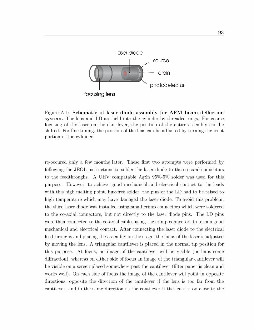
93
Figure A.1: Schematic of laser diode assembly for AFM beam deflectionsystem. The lens and LD are held into the cylinder by threaded rings. For coarsefocusing of the laser on the cantilever, the position of the entire assembly can beshifted. For fine tuning, the position of the lens can be adjusted by turning the frontportion of the cylinder.
re-occured only a few months later. These first two attempts were performed by
following the JEOL instructions to solder the laser diode to the co-axial connectors
to the feedthroughs. A UHV compatable AgSn 95%-5% solder was used for this
purpose. However, to achieve good mechanical and electrical contact to the leads
with this high melting point, flux-free solder, the pins of the LD had to be raised to
high temperature which may have damaged the laser diode. To avoid this problem,
the third laser diode was installed using small crimp connectors which were soldered
to the co-axial connectors, but not directly to the laser diode pins. The LD pins
were then connected to the co-axial cables using the crimp connectors to form a good
mechanical and electrical contact. After connecting the laser diode to the electrical
feedthroughs and placing the assembly on the stage, the focus of the laser is adjusted
by moving the lens. A triangular cantilever is placed in the normal tip position for
this purpose. At focus, no image of the cantilever will be visible (perhaps some
diffraction), whereas on either side of focus an image of the triangular cantilever will
be visible on a screen placed somewhere past the cantilever (filter paper is clean and
works well). On each side of focus the image of the cantilever will point in opposite
directions, opposite the direction of the cantilever if the lens is too far from the
cantilever, and in the same direction as the cantilever if the lens is too close to the
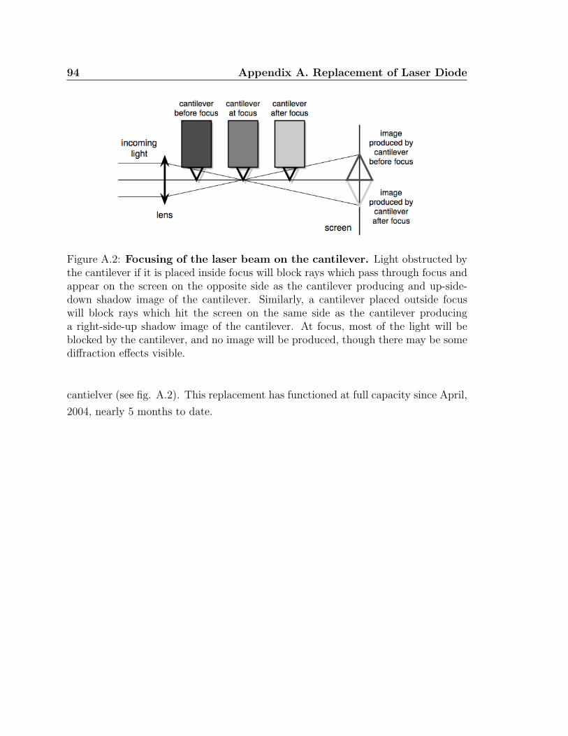
94 Appendix A. Replacement of Laser Diode
Figure A.2: Focusing of the laser beam on the cantilever. Light obstructed bythe cantilever if it is placed inside focus will block rays which pass through focus andappear on the screen on the opposite side as the cantilever producing and up-side-down shadow image of the cantilever. Similarly, a cantilever placed outside focuswill block rays which hit the screen on the same side as the cantilever producinga right-side-up shadow image of the cantilever. At focus, most of the light will beblocked by the cantilever, and no image will be produced, though there may be somediffraction effects visible.
cantielver (see fig. A.2). This replacement has functioned at full capacity since April,
2004, nearly 5 months to date.
Appendix B
LEED of C60 on KBr(001) surface
The sample was prepared in the same manner as the samples investigated by NC-
AFM. A coverage of 0.2 ML was deposited on a fresh KBr(001) surface cleaved in
vacuum at a rate of ∼0.004 ML/s. Electron beam energies which were sufficiently
large to prevent charging of the surface were used. Exposure to the beam was min-
imized as much as possible. The sample had no visual indications of damage (eg.
colour change or cloudiness) after being removed from the vacuum system.
Although only a few spots can be seen in the images acquired due to both camera
focus and possibly LEED focus, also resulting in some broadness of the LEED spots,
there seems to be a two-fold symmetry in the diffraction pattern. Due to the poor
quality of the LEED results combined with the expected complexity of the structures
formed by C60 on the KBr(001) surface further analysis was not attempted. How-
ever, the ability to acquire any LEED pattern on this type of sample indicates that
with greater attention to the special considerations required to perform LEED on
insulating samples, a determination of the C60 structure on KBr should be possible.
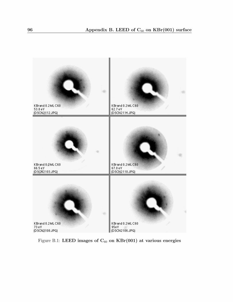
96 Appendix B. LEED of C60 on KBr(001) surface
Figure B.1: LEED images of C60 on KBr(001) at various energies
Appendix C
Prediction Algorithm for Epitaxy
of Molecular systems
By modelling the two lattices as plane waves, a real-space analytic expression can be
obtained to describe the degree of epitaxy, or phase coherence, between the overlayer
and substrate (ie, commensurism vs. coincidence vs. incommensurism). The follow-
ing expression produces a dimensionless energy which returns the values 0 (-0.5 on
hexagonal substrates), 0.5, and 1, for commenusrism, coincidence I, and incommen-
surism respectively [65].
Vinterface
V0
= 1−[sin(Mπp)
sin(πp)
sin(Nπr)
sin(πr)+
sin(Mπq)
sin(πq)
sin(Nπs)
sin(πs)
] [1
2NM
](C.1)
Where p, q, r, s are the matrix elements of C as described previously, and N × M
(where M and N are odd numbers) defines the size of overlayer lattice examined.
This expression can be used to classify known structures, as well as predict possi-
ble commensurate and coincidence I structures based on expected overlayer lattice
constants. Note that the function cannot discern coincidence II structrures as there
is no column of the matrix C which consists of integers, and hence Vinterface/V0 will
take on the same value as for an incommensurate structure. In this case the matrix

98 Appendix C. Prediction Algorithm for Molecular Epitaxy
elements p, q, r, s must be examined.
A plot of Vinterface/V0 as a function of angle, or lattice constant or both will show
where the function reaches the values 0 and 0.5 revealing where commensurate and
coincident structures (respectively) are possible. A program was written in Fortran77
to find commensurate and coincidence-I structures in a similar way varying both θ, the
overlayer rotation angle, and the overlayer lattice constant (where b1 = b2, and both
change at the same time and β is held constant, exploring an isotropic deformation
of the overlayer lattice). The “figure-of-merit” function Vinterface/V0, and the matrix
elements p, q, r, s were calculated for a range of overlayer rotation angles for varying
lattice constatns. To avoid numerical difficulties around the regions of the function
where 0/0 occurs, L’Hopital’s rule is applied within the code, replacing the expression
which produces 0/0 with the appropriate limit:
sin(Nπp)
sin(πp)=
0
0−→ N (C.2)
To access the full range of variable lattice parameters, the program was modified to
include separately varying lattice constants b1 and b2, as well as the angle between the
overlayer lattice vectors β, and again the overlayer rotation angle θ. Since four pa-
rameters are now being varied, only incidences of commensurism (Vinterface/V0 = 0),
and coincidence-I (Vinterface/V0 = 0.5) are recorded along with the values of b1, b2, β
and θ where these instances occur, the matrix elements p, q, r, s and the actual value
of Vinterface/V0.
All versions of the code were tested with an input of two identical hexagonal lattices,
returning commensurism for all values of θ which are multiples of 60 and identical
lattice parameters.
The prediction algorithm was applied to the C60 on KBr system. Lattice constants of
the KBr were input as: a1 = a2 = 4.6669A for the primitive cell, and α = 90. The
C60 lattice was varied over: 9.600A < b1, b2 < 10.400A varied independently in steps
of 0.004A, with β varied from 57.00 to 63.00 in steps of 0.04. The overlayer rotation
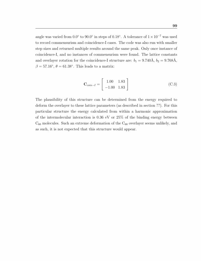
99
angle was varied from 0.0 to 90.0 in steps of 0.18. A tolerance of 1×10⁻⁷ was used
to record commensurism and coincidence-I cases. The code was also run with smaller
step sizes and returned multiple results around the same peak. Only once instance of
coincidence-I, and no instances of commensurism were found. The lattice constants
and overlayer rotation for the coincidence-I structure are: b1 = 9.740A, b2 = 9.768A,
β = 57.16, θ = 61.38. This leads to a matrix:
Ccoin−I =
[1.00 1.83
−1.00 1.83
](C.3)
The plausibility of this structure can be determined from the energy required to
deform the overlayer to these lattice parameters (as described in section ??). For this
particular structure the energy calculated from within a harmonic approximation
of the intermolecular interaction is 0.36 eV or 25% of the binding energy between
C60 molecules. Such an extreme deformation of the C60 overlayer seems unlikely, and
as such, it is not expected that this structure would appear.
Appendix D
Lattice structure prediction
algorithm code
Source code written in FORTRAN77, compiled in UNIX. Standard input
file below.
PROGRAM LATTICE_STRUCTURE_v3
! *****************************************************************!! Calculates the value of the analytic "figure of merit" function! (dimensionless interface potential Vint)!! version 3 adds independantly variable overlayer lattice parameters! (including beta)!! Defualt input file is lattice5.in! Input angle values are in degrees! Program contains subroutines: (none)!! *****************************************************************
IMPLICIT DOUBLE PRECISION (a-h, o-z)PARAMETER (pi=3.141592654)

101
PARAMETER (nptsx=10)PARAMETER (nptsy=5000)DIMENSION xrecord(nptsx,nptsy)
read(5,*) a1, a2, alpharead(5,*) b1, b2, betaread(5,*) delb1,delb2,delbetaread(5,*) mm, nnread(5,*) thstart, thendread(5,*) nb, nbeta, nthetaread(5,*) tolread(5,*) nout
open(6, file="lattice4.ERR", status=’unknown’)
thstartr=thstart*pi/180thendr=thend*pi/180thstep=(thendr-thstartr)/ntheta
if (nb.eq.0) thenb1step=0.0d+00b2step=0.0d+00
elseb1step=(2*delb1)/nbb2step=(2*delb2)/nb
end if
den1=a1*sin(alpha*pi/180)den2=a2*sin(alpha*pi/180)
alphar=alpha*pi/180betar=beta*pi/180delbetar=delbeta*pi/180
if (nbeta.eq.0) thenbetastepr=0.0d+00
elsebetastepr=(2*delbetar)/nbeta
end if
do i=1,(nb+1)xb1=(b1-delb1)+b1step*(i-1)do j=1,(nb+1)
xb2=(b2-delb2)+b2step*(j-1)
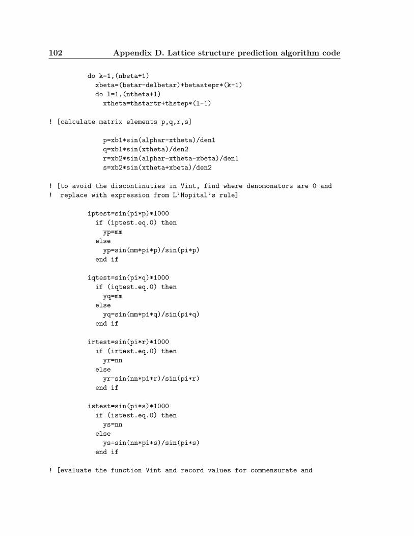
102 Appendix D. Lattice structure prediction algorithm code
do k=1,(nbeta+1)xbeta=(betar-delbetar)+betastepr*(k-1)do l=1,(ntheta+1)xtheta=thstartr+thstep*(l-1)
! [calculate matrix elements p,q,r,s]
p=xb1*sin(alphar-xtheta)/den1q=xb1*sin(xtheta)/den2r=xb2*sin(alphar-xtheta-xbeta)/den1s=xb2*sin(xtheta+xbeta)/den2
! [to avoid the discontinuties in Vint, find where denomonators are 0 and! replace with expression from L’Hopital’s rule]
iptest=sin(pi*p)*1000if (iptest.eq.0) thenyp=mm
elseyp=sin(mm*pi*p)/sin(pi*p)
end if
iqtest=sin(pi*q)*1000if (iqtest.eq.0) thenyq=mm
elseyq=sin(mm*pi*q)/sin(pi*q)
end if
irtest=sin(pi*r)*1000if (irtest.eq.0) thenyr=nn
elseyr=sin(nn*pi*r)/sin(pi*r)
end if
istest=sin(pi*s)*1000if (istest.eq.0) thenys=nn
elseys=sin(nn*pi*s)/sin(pi*s)
end if
! [evaluate the function Vint and record values for commensurate and
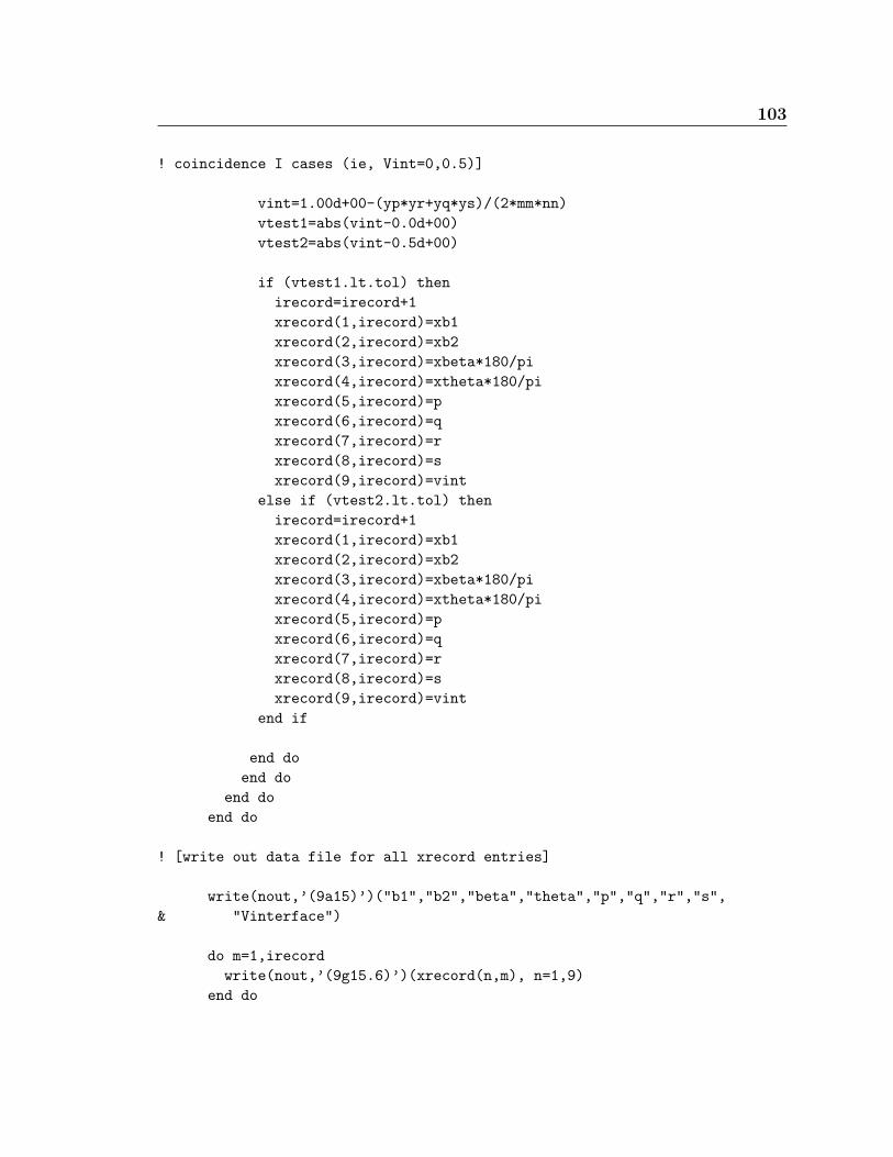
103
! coincidence I cases (ie, Vint=0,0.5)]
vint=1.00d+00-(yp*yr+yq*ys)/(2*mm*nn)vtest1=abs(vint-0.0d+00)vtest2=abs(vint-0.5d+00)
if (vtest1.lt.tol) thenirecord=irecord+1xrecord(1,irecord)=xb1xrecord(2,irecord)=xb2xrecord(3,irecord)=xbeta*180/pixrecord(4,irecord)=xtheta*180/pixrecord(5,irecord)=pxrecord(6,irecord)=qxrecord(7,irecord)=rxrecord(8,irecord)=sxrecord(9,irecord)=vint
else if (vtest2.lt.tol) thenirecord=irecord+1xrecord(1,irecord)=xb1xrecord(2,irecord)=xb2xrecord(3,irecord)=xbeta*180/pixrecord(4,irecord)=xtheta*180/pixrecord(5,irecord)=pxrecord(6,irecord)=qxrecord(7,irecord)=rxrecord(8,irecord)=sxrecord(9,irecord)=vint
end if
end doend do
end doend do
! [write out data file for all xrecord entries]
write(nout,’(9a15)’)("b1","b2","beta","theta","p","q","r","s",& "Vinterface")
do m=1,irecordwrite(nout,’(9g15.6)’)(xrecord(n,m), n=1,9)
end do

104 Appendix D. Lattice structure prediction algorithm code
END
Standard input file:
4.6669,4.6669,9010.0,10.0,600.4,0.4,3.0155,1550.0,90.0200,150,5001.0d-0752
*************************************************************************
INSTRUCTIONS FOR INPUT FILE:
The variables are to be entered in the following order:
a1,a2,alpha *lattice parameters for substrateb1,b2,beta *lattice parameters for overlayerdelb1,delb2,delbeta *range of variation of overlayer lattice parammm,nn *size of overlayer mm x nnthstart,thend *overlayer rotation angles (thstart.. thend)nb,nbeta,ntheta *number of samples in b,beta, and theta resp.tol *sensitivity of coincidence detectionnout *number of output file (fort.nout)
NOTES:*alpha,beta,thstart,thend are input in degrees*mm and nn must be odd numbers
************************************************************************
Appendix E
Code for electrostatic kink sitepotential calculation
Source code written in FORTRAN77, compiled in UNIX. Standard input filebelow.
PROGRAM KINKPOTL_V3
! Program calculates the electrostatic potential at a kink site in a cubic! ionic crystal.! Returns 3 cross-section <100>, <010>, <111>, and the potential at all! points in an array.! Returns the energy landscape for a polarized C60 molecule!
IMPLICIT DOUBLE PRECISION (a-h, o-z)INTEGER z1,z2PARAMETER (nptssm=500)PARAMETER (nptslg=1000)DIMENSION z1(nptssm,nptssm)DIMENSION z2(nptssm,nptssm)DIMENSION vt(nptslg,nptslg)DIMENSION energy(nptslg,nptslg)DIMENSION xcross(10,nptslg)
read(5,*) nn, nmesh
106 Appendix E. Code for electrostatic kink site potential calculation
read(5,*) height, ithickread(5,*) rscaleread(5,*) alpharead(5,*) noutread(5,*) nprint
open(6, file="kinkpotl0.err", status=’unknown’)
qscale=1.6d-19ck=9.0d+9
! [initialize arrays z1, z2, vt, energy]
do i0=1,nndo j0=1,nn
z1(i0,j0)=0z2(i0,j0)=0
end doend do
do ix=1,nn*nmeshdo iy=1,nn*nmesh
vt(ix,jy)=0.0d+00energy(ix,jy)=0.0d+00
end doend do
! [create z2 array -- flat sheet of ions]
print *, "z2 array, first 6 columns:"
do i=1,nndo j=1,nn
z2(i,j)=(-1)**(i+j)! print *, "i=",i, " j=",j, " z2=",z2(i,j)
end doend do
! do ip1=1,nn! print *, z2(1,ip1), z2(2,ip1), z2(3,ip1), z2(4,ip1), z2(5,ip1),! +z2(6,ip1)! end do
! [create z1 array -- kink layer]
107
print *, "z1 array, first 6 columns:"
do i=1,nndo j=1,nn
if ((j.le.(nn/2)).and.(i.le.(nn/2))) thenz1(i,j)=-z2(i,j)
else if ((j.ge.(nn/2)).and.(i.le.(nn/2-1))) thenz1(i,j)=-z2(i,j)
end ifend do
end do
! do ip2=1,nn! print *, z1(1,ip2), z1(2,ip2), z1(3,ip2), z1(4,ip2), z1(5,ip2),! +z1(6,ip2)! end do
! [calculate the potential on a mesh of nn*nmesh]
do ix=1,nn*nmeshdo jy=1,nn*nmesh
do i=1,nndo j=1,nn
do k=1,ithickx=dble(ix)/dble(nmesh)y=dble(jy)/dble(nmesh)xdel=(x-dble(i))*rscaleydel=(y-dble(j))*rscaleif ((j.le.(nn/2)).and.(i.le.(nn/2))) then
z0=-1.0d+00+heightelse if ((j.ge.(nn/2)).and.(i.le.(nn/2-1))) then
z0=-1.0d+00+heightelse
z0=-2.0d+00+heightend ifxk=dble(k)zdel=(-xk-z0)*rscaler=sqrt(xdel**2+ydel**2+zdel**2)if (k.eq.1) then
qijk=z1(i,j)*qscaleelse
qijk=z2(i,j)*qscale*(-1)**kend if
108 Appendix E. Code for electrostatic kink site potential calculation
vt(ix,jy)=vt(ix,jy)+ck*qijk/rend do
end doend do
end doend do
! [calculate derivative and find energy for polarized C60]
do ix=1,(nn*nmesh-1)do jy=1,(nn*nmesh-1)
dx=(vt(ix,jy)-vt((ix+1),jy))/(rscale/nmesh)dy=(vt(ix,jy)-vt(ix,(jy+1)))/(rscale/nmesh)energy(ix,jy)=-alpha*(dx**2+dy**2)
end doend do
! [create cross-section arrays for <100>,<010>,<111> el potl, and energy]
do i1=1,nn*nmeshxcross(1,i1)=i1*rscale/nmesh/1.0d-06xcross(2,i1)=vt(i1,((nn+1)/2*nmesh))xcross(3,i1)=energy(i1,((nn+1)/2*nmesh))xcross(4,i1)=vt(((nn+1)/2*nmesh),i1)xcross(5,i1)=energy(((nn+1)/2*nmesh),i1)xcross(6,i1)=sqrt(2.0)*i1*rscale/nmesh/1.0d-06xcross(7,i1)=vt(i1,i1)xcross(8,i1)=energy(i1,i1)xcross(9,i1)=vt(2,i1)
end do
! [print out full array if specified]
if (nprint.eq.0) thendo ll=1,nn*nmesh
write(nout+1,’(1000g15.6)’)(vt(kk,ll), kk=1,(nn*nmesh))end dodo ll=1,(nn*nmesh-1)
write(nout+2,’(1000g15.6)’)(energy(kk,ll), kk=1,(nn*nmesh-1))end do
end if
! [print out cross-section (always)]

109
write(nout,’(10a15)’)("x1/ang","V100", "energy100", "V010",+"energy010", "x2/ang","V111", "energy111",+"1col")
do ll=1,nn*nmeshwrite(nout,’(10g15.6)’)(xcross(kk,ll), kk=1,9)
end do
END
Standard input file:
30, 100.5d+00, 103.3d-06522e-30540
**********************************************************************
INPUT FILE FOR KINKPOTL_V2:
nn, nmeshheight, ithickrscalealphanoutnprint
nn *number of ions, integer, must be EVEN number, max 500nmesh *multiplier of nn to determine number of mesh points for potential,
integer, even, max to give nn*nmesh=10 000 (10 recommended)height *dble, height above surface in l.c.ithick *integer, number of layers in calculationrscale *dble, interionic distance in metersnout *integer, gives first file name as fort.noutnprint *if 0, full array of potntial is printed as fort.(nout+1)
if 1, only cross-sections are printed in fort.nout**********************************************************************

Bibliography
[1] G. Binnig and H. Rohrer. Scanning tunneling microscope. Helvetica PhysicaActa, 55:726–735, 1982.
[2] F. Rosei, M. Schunack, Y. Naitoh, P. Jiang, A. Gourdon, E. Laegsgaard, I. Stens-gaard, C. Joachim, and F. Besenbacher. Properties of large organic moleculeson metal surfaces. Progress in Surface Science, 71:95–146, 2003.
[3] A. Aviram and M. A. Ratner. Molecular Rectifiers. Chemical Physics Letters,29(2):277–283, 1974.
[4] A. Asenjo, A. Baro, X. Borrise, J. Colchero, A. Correia, I. Diez-Perez,R. Fernandez, X. Fernandez-Busquets, A. Gil, J. Gomez, G. Gomila,F. Hernandez, P. Martınez Amper, J. Mendez, J. Pascual, F. Perez-Murano,R. Reifenberger, F. Rico, C. Roldan, J. Samitier, and F. Sanz. Scanning ProbeMicroscopy: Basic Concepts and Applications. Phantoms IST NanoelectronicsNetwork, September 2003. Available from http://www.phantomsnet.com.
[5] Private communications with H. Abruna (Cornell University).
[6] M. Mobus, N. Karl, and T. Kobayashi. Structure of perylene-tetracarboxyllicdianhydride thin films on alkali halide crystal substrates. J. of Crystal Growth,116:495–504, 1992.
[7] S. R. Forrest, P. E. Burrows, E. I. Haskal, and F. F. So. Ultrahigh-vacuumquasiepitaxial growth of model van der waals thin films. II. Experiment. PhysicalReview B, 49(16):11 309–11 321, 1994.
[8] S. R. Forrest and P. E. Burrows. Growth modes of organic semiconductor thinfilms using organic molecular beam deposition: epitaxy, van der waals epitaxyand quasi-epitaxy. Supramolecular Science, 4(1–2):127–139, 1997.
BIBLIOGRAPHY 111
[9] K. Yase, N. Ara-Kato, T. Hanada, H. Takiguchi, Y. Yoshida, G. Back, K. Abe,and N. Tanigaki. Aggregation mechanism in fullerene thin films on several sub-strates. Thin Solid Films, 331:131–140, 1998.
[10] F. J. Giessibl. Atomic resolution of the Silicon(111) 7×7 surface by Atomic ForceMicroscopy. Science, 267:68–71, 1995.
[11] Shin–ichi Kitamura and Masashi Iwatsuki. Observation of 7×7 reconstructedstructure on the Silicon (111) surface using ultrahigh vacuum noncontact atomicforce microscopy. Jpn. J. Appl. Phys., 34:L145–L148, 1995.
[12] Harald Brune. Microscopic view of epitaxial metal growth: nucleation and ag-gregation. Surf. Sci. Rep., 31:121–229, 1998.
[13] G. Binnig, H. Rohrer, Ch. Gerber, and E. Weibel. 7×7 reconstruction on Si(111)resolved in real space. Phys. Rev. Lett., 50(2):120–123, 1983.
[14] G. Binnig and C.F. Quate. Atomic force microscope. Phys. Rev. Lett., 56(9):930–933, 1986.
[15] C.M. Mate, G.M. McClelland, Ragnar Erlandsson, and Shirley Chiang. Atomicscale friction of a tungsten tip on a graphite surface. Phys. Rev. Lett., 59(17):120–123, 1987.
[16] G. Binnig, Ch. Gerber, E. Stoll, T.R. Albrecht, and C.F. Quate. Atomic resolu-tion with atomic force microscope. Europhysics Letters, 3(12):1281–1286, 1987.
[17] T.R. Albrecht, P. Grutter, D. Horne, and D. Rugar. Frequency modulationdetection using high-Q cantilevers for enhanced force microscope sensitivity. J.Appl. Phys, 68(2):668–673, 1991.
[18] Image taken from Canadian National Institute for the Blind website:http://cnib.ca.
[19] E. Gnecco, R. Bennewitz, T. Gyalog, Ch. Loppacher, M. Bammerlin, E. Meyer,and H.-J. Gu ntherodt. Velocity dependence of atomic friction. Phys. Rev. Lett.,84(6):1172–1175, 2000.
[20] A. Socoliuc, R. Bennewitz, E. Gnecco, and E. Meyer. Transition from stick-slip to continuous sliding in atomic friction: Entering a new regime of ultralowfriction. Physical Review Letters, 92(13):134301, 2003.
[21] J. M. LeDue, H. J. Kreuzer, S. A. Burke, M. H. Jericho, and J. C. Neima.Dynamical modeling of STM manipulation of molecules on surfaces. SurfaceScience, 538:L465–L470, 2003.
112 BIBLIOGRAPHY
[22] Masami Kageshima, Hisato Ogiso, and Hiroshi Tokomoto. Lateral forces dur-ing manipulation of a single C60 molecule on the Si(001)-2×1 surface. SurfaceScience, 517:L557–L562, 2002.
[23] M. Guggisberg, M. Bammerlin, Ch. Loppacher, O. Pfeiffer, A. Abdurixit, V. Bar-wich, R. Bennewitz, A. Baratoff, E. Meyer, and H. J. Guntherodt. Separationof interactions by noncontact atomic force microscopy. Phys. Rev. B, 61(16):11151, 2000.
[24] U. Durig. Extracting interaction forces and complementary observables in dy-namic probe microscopy. Appl. Phys. Lett., 76:1203–1205, 2000.
[25] F. J. Giessibl. A direct method to calculate tip-sample forces from frequencyshifts in frequency-modulation atomic force microscopy. Appl. Phys. Lett.,78:123–125, 2001.
[26] M. Nonnemacher, M. P. O’Boyle, and H. K. Wickramasinghe. Kelvin probe forcemicroscopy. Appl. Phys. Lett., 58(25):2921–2923, 1991.
[27] S. Morita, R. Weisendanger, and E. Meyer. Non-contact atomic force microscopy.Springer, Berlin, 2002.
[28] J. M. Mativetsky, S. A. Burke, R. Hoffmann, Y. Sun, and P. Grutter. Molecularresolution imaging of C60 on Au(111) by non-contact atomic force microscopy.Nanotechnology (Special Issue–NC-AFM proceedings), 15(2):S40–S43, 2003.
[29] T. Arai and M. Tomitori. Bias dependence of Si(111)7×7 images observed bynoncontact atomic force microscopy. Applied Surface Science, 157:207–211, 2000.
[30] John A. Venables. Introduction to Surface and Thin Film Processes. CambridgeUniversity Press, Cambridge, 2000.
[31] Celeste Sagui and Martin Grant. Theory of nucleation and growth during phaseseparation. Phys. Rev. E, 59(4):4175–4187, 1999.
[32] Zhenyu Zhang and Max G. Lagally. Atomistic processes in the early stages ofthin-film growth. Science, 276:377–383, 1997.
[33] D. E. Hooks, T. Fritz, and M. D. Ward. Epitaxy and molecular organization onsolid substrates. Advanced Materials, 13(4):227–241, 2001.
[34] S. R. Forrest and Y. Zhang. Ultrahigh-vacuum quasiepitaxial growth of modelvan der waals thin films. I. Theory. Physical Review B, 49(16):11 297–11 308,1994.
BIBLIOGRAPHY 113
[35] J. Vogt and H. Weiss. The structure of KBr(100) and LiF(100) single crystalsurfaces: a tensor low energy electron diffraction analysis. Surface Science,501:203–213, 2002.
[36] KBr properties available on Korth Kristalle website: http://www.korth.de.
[37] H. W. Kroto, J. R. Heath, S. C. O’Brien, R. F. Curl, and R. E. Smaley. C60:Buckminsterfullerene. Nature, 318:162–163, 1985.
[38] M. S. Dresselhaus, G. Dresselhaus, and P.C. Eklund. Science of Fullerenes andCarbon Nanotubes. Academic Press, San Diego, 1996.
[39] M. Bammerlin, R. Luthi, and et. al. True atomic resolution on the surface of aninsulator via ultra-high vacuum dynamic force microscopy. Probe Microscopy,1:3–9, 1997.
[40] C. Joachim and J. K. Gimzewski. An electromechanical amplifier using a singlemolecule. Chem. Phys. Lett., 265:353–357, 1997.
[41] H. Park, J. Park, A. Lim, E. Anderson, P. Alivisatos, and P. McEuen. Nanome-chanical oscillations in a single-C60 transistor. Nature, 407:57–60, 2000.
[42] R. Luthi, E. Meyer, H. Haefke, L. Howald, W. Gutmannsbauer, and H.-J.Guntherodt. Sled-type motion on the nanometer scale: Determination of dissi-pation and cohesive energies of C60. Science, 266:1979–1981, 1994.
[43] K. Tanigaki, S. Kuroshima, and T. Ebbensen. Crystal growth and structure offullerene thin films. Thin Solid Films, 257:154–165, 1995.
[44] Heating parent holder designed by Dr. Regina Hoffmann based on the standardparent holder supplied by JEOL. Parts machined at Basel University, Switzer-land.
[45] Density of C60 as stated on MSDS provided by Alfa Aesar.
[46] E. Meyer, R. M. Overney, K. Dransfeld, and T. Gyalog. Nanoscience: Frictionand Rheology on the Nanometer Scale. World Scientific, New Jersey, 1998.
[47] A.P. French. Vibrations and Waves. W.W. Norton and Co., New York, 1971.
[48] Regina Hoffmann. Magnetic and Interatomic Forces Measured by Low Temper-ature Scanning Force Microscopy. PhD thesis, Universitat Basel, 2001.
[49] R. Wiesendanger and H.-J. Guntherodt. Scanning Tunneling Mircoscopy II, Vol.28 of Springer Series in Surface Science. Spinger-Verlag, Heidelberg, 1992.
114 BIBLIOGRAPHY
[50] Dominik Brandlin, Robert Sum, and Vicki Connolly. easyPLL FM Sensor Con-troller. nanoSurf, Switzerland.
[51] Y. Leng, C. C. Williams, L. C. Su, and G. B. Stringfellow. Atomic ordering ofGaInP studied by kelvin probe force microscopy. Appl. Phys. Lett., 66(10):1264–1266, 1995.
[52] Sascha Sadewasser and Martha Ch. Lux-Steiner. Correct height measurementin noncontact atomic force microscopy. Physical Review Letters, 91(26):266101,2003.
[53] J. Vogt and H. Weiss. The structure of NaCl(100) and KCl(100) single crystalsurfaces: a tensor low energy electron diffraction analysis. Surface Science,491:155–168, 2001.
[54] Martin Dube Yi Sang and Martin Grant. Thermal effects on atomic friction.Phys. Rev. Lett., 87(17):174301–1–4, 2001.
[55] L. Nony, E. Gnecco, A. Baratoff, A. Alkauskas, R. Bennewitz, O. Pfeiffer,S. Maier, A. Wetzel, E. Meyer, and Ch. Gerber. Observation of individualmolecules trapped on a nanostructured insulator. NanoLetters, 4, 2004.
[56] Bartosz Such, Pawel Czuba, Piotr Piatkowski, and Marek Szymonski. AFMstudies of electron-stimulated desorption process of KBr(001) surface. SurfaceScience, 451:203–207, 2000.
[57] M. Szymonski, J. Kolodziej, B. Such, P. Piatkowski, P. Struski, P. Czuba, andF. Krok. Nano-scale modification of ionic surfaces induced by electronic transi-tions. Progress in Surface Science, 67:123–138, 2001.
[58] R. Bennewitz, S. Schar, V. Barwich, O. Pfeiffer, E. Meyer, F. Krok, B. Such,J. Kolodzej, and M. Szymonski. Atomic-resolution images of radiation damagein KBr. Surface Science Letters, 474:L197–L202, 2001.
[59] On Man Leung and M. Cynthia Goh. Orientational ordering of polymers byatomic force microscope tip–surface interaction. Science, 255:64–66, 1992.
[60] A. Socoliuc, E. Gnecco, R. Bennewitz, and E. Meyer. Ripple formation inducedin localized abrasion. Physical Review B, 68:115416, 2003.
[61] J. A. Venables. Nucleation and growth of thin films. Rep. Prog. Phys., 47:399–459, 1984.
[62] Silvere Akamatsu, Gabriel Faivre, and Thomas Ihle. Symmetry broken doublefingers and seaweed patterns in thin-film directional solidification of a nonfacetedcubic crystal. Phys. Rev. E, 51(5):4751–4773, 1995.
BIBLIOGRAPHY 115
[63] B. Utter, R. Ragnarsson, and E. Bodenschatz. Alternating tip splitting in direc-tional solidification. Phys. Rev. Lett., 86:4604–4607, 2001.
[64] Nikolas Provatas, Quanyong Wang, Mikko Haataja, and Martin Grant. Sea-weed to dendrite transition in directional solidification. Phys. Rev. Lett.,91(15):155502, 2003.
[65] A. C. Hillier and M. D. Ward. Epitaxial interactions between molecular over-layers and ordered substrates. Physical Review B, 54(19):14037–14051, 1996.
[66] L. A. Girifalco. Molecular properties of C60 in the gas and solid phases. J. Phys.Chem., 96:858–861, 1992.
[67] Eric W. Weisstein. Truncated icosahedron. From MathWorld–A Wolfram webresource. http://mathworld.wolfram.com/TruncatedIcosahedron.html.
[68] E. I. Altman and R. J. Colton. Nucleation, growth and structure of fullerenefilems on Au(111). Surface Science, 279:49–67, 1992.
[69] E. I. Altman and R. J. Colton. The interaction of C60 with noble metal surfaces.Surface Science, 295:13–33, 1993.
[70] W. W. Pai, C-L Hsu, M.C. Lin, K.C. Lin, and T.B. Tang. Structural relaxationof adlayers in the presence of adsorbate-induced reconstruction: C60/Cu(111).Physical Review B, 69:125405, 2004.
[71] M. Grobis, X. Lu, and M. F. Crommie. Local electronic properties of a molecularmonolayer C60 on Ag(001). Physical Review B, 66:161408, 2002.
[72] X. Lu, M. Grobis, K. H. Khoo, S. G. Louie, and M. F. Crommie. Spatially map-ping the spectral density of a single C60 molecule. Phys. Rev. Lett., 90(9):096802,2004.
[73] Shin’ichi Kitamura, Katsuyuki Suzuki, and Masashi Iwatsuki. Measurement ofcontact potential difference using an ultrahigh vacuum noncontact atomic forcemicroscope. JEOL News, 34E(1):53–57, 1999.
[74] M. Bohringer, W-D. Schneider, and R. Berndt. Scanning tunneling microscope–induced molecular motion and its effect on the image formation. Surface Science,408:72–85, 1998.
[75] S. Berner, M. Brunner, L. Ramoino, H. Suzuki, H.-J. Guntherodt, and T. A.Jung. Time evolution of a 2D solid-gas equilibrium: a model system for molecularadsorption and diffusion. Chem. Phys. Lett., 348:175–181, 2001.
116 BIBLIOGRAPHY
[76] David J. Griffiths. Introduction to Electrodynamics: 3rd Edition. Prentice-Hall,New Jersey, 1999.
[77] M.R. Pederson, A.A. Quong, J.Q. Broughton, and J.L. Feldman. Fullerenemolecules and tubules: Polarizabilities, vibrational modes and nanocapillarity.Computational Materials Science, 2:536–542, 1994.
[78] Lasse Jensen, Per-Olaf Astrand, and Kurt V. Mikkelsen. Microscopic and macro-scopic polarization in c60 fullerene clusters as calculated by an electrostatic in-teraction molecule. J. Phys. Chem. B, 108:8226–8233, 2004.
[79] N. Oyabu, O. Custance, I. Yi, Y. Sugawara, and S. Morita. Mechanical verticalmanipulation of selected single atoms by soft nanoindentation using near contactatomic force microscopy. Phys. Rev. Lett., 90, 2003.
[80] Noriaki Oyabu, Yoshiaki Sugimoto, Oscar Custance, Masayuki Abe, and SeizoMorita. Using noncontact atomic force microscopy for laterally manipulatingsingle atoms at semiconductor surfaces. Presented at the 7th International Non-contact Atomic Force Microscopy Conference, Seattle USA, September 2004.