broadband surface-wave transformation cloaksoljacic/surface-cloak_pnas.pdf · 2015-06-28 · 2 the...
TRANSCRIPT
1
Broadband surface-wave transformation cloak
Su Xu†1,2, Hongyi Xu†3,4, Hanhong Gao5, Yuyu Jiang1,2, Faxin Yu6, John D.
Joannopoulos7, Marin Soljačić7, Hongsheng Chen*1,2,7, Handong Sun*3,4, and Baile
Zhang*3,4
1State Key Laboratory of Modern Optical Instrumentation, Zhejiang University, Hangzhou 310027, China
2The Electromagnetics Academy at Zhejiang University, Department of Information Science & Electronic
Engineering, Zhejiang University, Hangzhou 310027, China 3Division of Physics and Applied Physics, School of Physical and Mathematical Sciences, Nanyang Technological
University, Singapore 637371, Singapore 4Centre for Disruptive Photonic Technologies, Nanyang Technological University, Singapore 637371, Singapore 5Department of Electrical Engineering and Computer Science, Massachusetts Institute of Technology, Cambridge,
MA 02139, United States 6School of Aeronautics and Astronautics, Zhejiang University, Hangzhou 310027, China 7Research Laboratory of Electronics, Massachusetts Institute of Technology, Cambridge, MA 02139, United
States.
†These two authors contributed equally to the work. *Authors to whom correspondence should be addressed; E-mail: [email protected] (H. Chen); [email protected] (H. Sun); [email protected] (B. Zhang)

2
Theability toguidesurfaceelectromagnetic (EM)wavesaroundsharp
cornersandothertypesofdisorder,withoutdisturbingthewaveamplitude
orphase,isingreatdemandformodernphotonicandplasmonicdevices1,2.
This is fundamentallydifficulttorealizebecause lightmomentummustbe
conserved inascatteringevent.Apartialrealizationhasbeenachievedby
exploiting topologicalEM surface states3-7,but this approach is limited to
narrow‐band light transmission and subject tophasedisturbances in the
presence of a corner or disorder8. Recent advances in transformation
optics9,10applyprinciplesof general relativity to curvethe spaceforlight,
allowing one to match the momentum and phase of light around any
disorder,asifthatdisorderwerenotthere.Thisfeaturehasbeenexploited
in the development of invisibility cloaks11-19. An ideal invisibility cloak,
however,wouldrequirethephasevelocityoflightbeingguidedaroundthe
"cloaked object" to exceed the vacuum speed of light – a feat potentially
achievable only overan extremely narrow band10,11,20. In this work we
theoretically and experimentally demonstrate that the bottlenecks
encounteredinpreviousstudiescanbeovercome.Weintroduceanewclass
of cloaks capable ofremarkable broadbandsurface EM waves guidance
around ultra‐sharp corners and bumps with no perceptible changes in
amplitude and phase. These cloaks consist ofspecifically designed
non‐magneticmetamaterials, and they achieve nearly ideal transmission
efficiencyoverabroadband frequencyrange from0+ to6GHz.Thiswork
provides strong support for the application of transformation optics to
plasmonic circuits, and could pave the way towards high performance,
large‐scaleintegratedphotoniccircuits.

3
One of the main limitations in plasmonic circuitry and devices1,2 that utilize
surface EM waves (surface plasmons at optical frequencies) as information and
energy carriers is the inability to perfectly guide surface EM waves around
unavoidable disorders such as sharp corners. While near-perfect transmission around
sharp corners in electronic circuits is routine, it is fundamentally difficult to realize
with surface waves because surface waves suffer from scattering loss when
encountering sharp corners or other irregular disorders.
“Scattering-free” guidance of surface waves around sharp corners has been
demonstrated only in topological EM surface states3-6. It has been developed in
analogy with electronic chiral edge states in quantum Hall systems21 and with
topological insulators22,23. In order to force the waves to circumvent disorders, the
studies cited above typically require the use of photonic crystals with substantial
magnetic responses. The use of magnetic metamaterials limits these realizations to a
narrow microwave frequency band. The use of conventional nonmagnetic photonic
materials, on the other hand, could allow for scalability to the optical regime with
broad bandwidth.
The difficulty in sharp bending is the dramatic momentum mismatch of surface
EM waves before and after passing the sharp corner in an extremely compact space.
Transformation optics9,10 allows for the design of inhomogeneous metamaterials that
control light by effectively warping the EM space analogously to the way gravity
curves space in general relativity. Since the concept of momentum stems essentially
from space homogeneity24, an effectively curved EM space provides a method to
match wave momenta by compensating for the asymmetry of spatial translation
around sharp corners. Surface EM waves can be thereby deceived as if they were still
propagating along a flat surface, without any corners.

4
In the past few years, transformation optics has been used to develop invisibility
cloaks to hide objects from free-space propagating EM waves11-19. However, an ideal
invisibility cloak is fundamentally narrow band because it would require the phase
velocity of light being guided around the “cloaked object” to exceed the vacuum
speed of light10,11,20. On the other hand, surface EM waves are essentially “slow”
waves, whose bending will not cause superluminal propagation in the majority of
situations. Yet all of the potential applications of transformation optics in surface EM
waves25-29 so far are still theoretical. Most theoretical designs only dealt with objects
with relatively smooth surfaces or finite bending radii25,26. Refs. 28 and 29 proposed
alternativesuface wavebending approaches; yet in general scattering will occur when
an ultra-sharp bending with zero radius is desired. Therefore, if a similar approach of
sharp bending could be realized for surface waves, many unique conceivable
applications would become feasible: not only waveguides for sharp right-angle
corners3, but also carpet cloaks that can hide irregular bumps on the metal/dielectric
interface26, super plasmonic resonators with extremely high Q values30, etc.
Here we present experimental demonstration of broadband sharp bending of
surface EM waves with almost ideal transmission; this allows “invisibility cloaking”
of disorders such as ultra-sharp corners and bumps for surface EM waves. The
remarkable broadband guidance, lacking in previous “scattering-free” topological EM
surface states and free-space invisibility cloaks, is because of two reasons. Firstly, the
“slow wave” property of surface EM waves can overcome the bottleneck of
free-space invisibility cloaks since its phase velocity does not need to exceed the
vacuum speed of light. Secondly, we adopt a fully non-magnetic design with naturally
accessible dielectric parameters, while magnetic responses were necessary to open the
topological band gap for topological EM surface states.

5
We start with the demonstration of bending a surface EM wave across sharp
right-angle corners at microwave frequencies—similar to the previous demonstration
of bending a guided topological surface EM wave in a photonic crystal3. We call the
bending adaptor a “corner cloak,” as it effectively hides a corner to the wave as if the
corner did not exist. Since metals at microwave frequencies are perfect electric
conductors that generally do not support surface EM waves, here we adopt the
approach of geometrically-induced, or “spoof,” surface plasmons31—i.e., we use a
grooved metallic surface (referred to as a “patterned metal” in Figs. 1, 2, 3) to support
surface EM waves in the microwave regime. Fig. 1a shows the experimental setup: a
U-shaped surface-wave waveguide (a metal base with periodic grooves on its surfaces:
i.e., the patterned metal) with two right-angle zero-radius corners. Given the sizes of
the cloaks, the more confined the surface waves on the dielectric-metal interface, the
better the cloaking performance. To enhance the confinement, we load the grooves with
ceramic material with permittivity ceramic= 21.We use glass with permittivity b=4.6 as
the surrounding background that is to be impedance-matched with the cloaks. More
details can be found in the Supplementary Information.
The two identical corner cloaks locate at the two corners. This structure that
consists of the U-shaped waveguide and two corner cloaks can be thought of as if it
were transformed from a straight waveguide without any corner. A corner cloak, when
transformed back, corresponds to a triangular space on top of the dielectric-metal
interface, whose area is purposely chosen to be the same as the corner cloak. This area
preservation guarantees non-magnetism in the cloak design for surface EM waves.
(See Supplementary Information for more details.) The two identical corner cloaks
require anisotropic constitutive parameters. For each cloak the required principal
permittivities in two orthogonal directions, and , after the procedure of
6
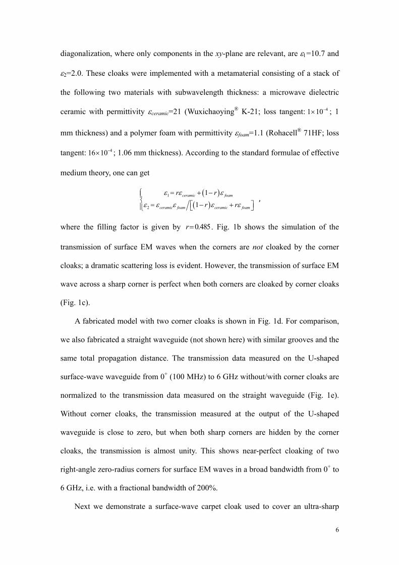
diagonalization, where only components in the xy-plane are relevant, are =10.7 and
=2.0. These cloaks were implemented with a metamaterial consisting of a stack of
the following two materials with subwavelength thickness: a microwave dielectric
ceramic with permittivity ceramic=21 (Wuxichaoying® K-21; loss tangent: 41 10 ; 1
mm thickness) and a polymer foam with permittivity foam=1.1 (Rohacell® 71HF; loss
tangent: 416 10 ; 1.06 mm thickness). According to the standard formulae of effective
medium theory, one can get
1
2
1
1
ceramic foam
ceramic foam ceramic foam
r r
r r ,
where the filling factor is given by 0.485r . Fig. 1b shows the simulation of the
transmission of surface EM waves when the corners are not cloaked by the corner
cloaks; a dramatic scattering loss is evident. However, the transmission of surface EM
wave across a sharp corner is perfect when both corners are cloaked by corner cloaks
(Fig. 1c).
A fabricated model with two corner cloaks is shown in Fig. 1d. For comparison,
we also fabricated a straight waveguide (not shown here) with similar grooves and the
same total propagation distance. The transmission data measured on the U-shaped
surface-wave waveguide from 0+ (100 MHz) to 6 GHz without/with corner cloaks are
normalized to the transmission data measured on the straight waveguide (Fig. 1e).
Without corner cloaks, the transmission measured at the output of the U-shaped
waveguide is close to zero, but when both sharp corners are hidden by the corner
cloaks, the transmission is almost unity. This shows near-perfect cloaking of two
right-angle zero-radius corners for surface EM waves in a broad bandwidth from 0+ to
6 GHz, i.e. with a fractional bandwidth of 200%.
Next we demonstrate a surface-wave carpet cloak used to cover an ultra-sharp
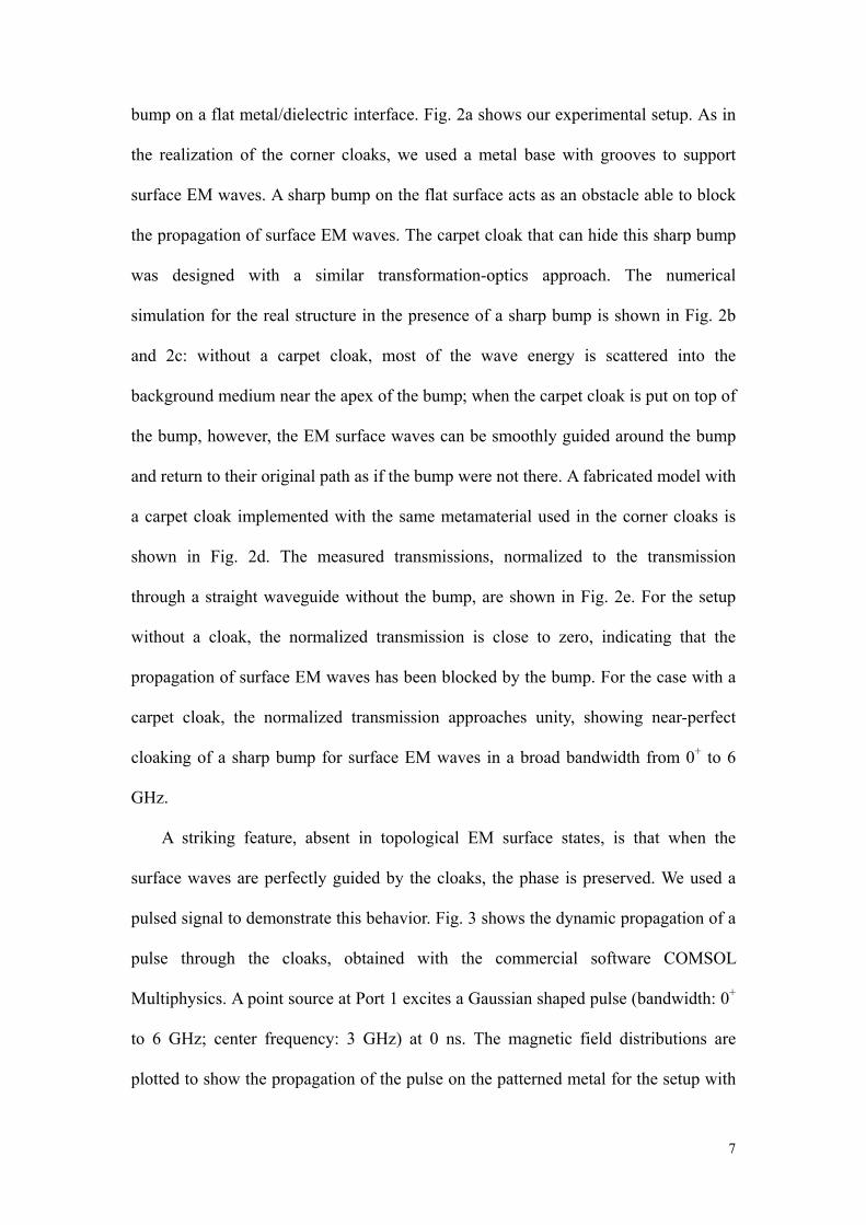
7
bump on a flat metal/dielectric interface. Fig. 2a shows our experimental setup. As in
the realization of the corner cloaks, we used a metal base with grooves to support
surface EM waves. A sharp bump on the flat surface acts as an obstacle able to block
the propagation of surface EM waves. The carpet cloak that can hide this sharp bump
was designed with a similar transformation-optics approach. The numerical
simulation for the real structure in the presence of a sharp bump is shown in Fig. 2b
and 2c: without a carpet cloak, most of the wave energy is scattered into the
background medium near the apex of the bump; when the carpet cloak is put on top of
the bump, however, the EM surface waves can be smoothly guided around the bump
and return to their original path as if the bump were not there. A fabricated model with
a carpet cloak implemented with the same metamaterial used in the corner cloaks is
shown in Fig. 2d. The measured transmissions, normalized to the transmission
through a straight waveguide without the bump, are shown in Fig. 2e. For the setup
without a cloak, the normalized transmission is close to zero, indicating that the
propagation of surface EM waves has been blocked by the bump. For the case with a
carpet cloak, the normalized transmission approaches unity, showing near-perfect
cloaking of a sharp bump for surface EM waves in a broad bandwidth from 0+ to 6
GHz.
A striking feature, absent in topological EM surface states, is that when the
surface waves are perfectly guided by the cloaks, the phase is preserved. We used a
pulsed signal to demonstrate this behavior. Fig. 3 shows the dynamic propagation of a
pulse through the cloaks, obtained with the commercial software COMSOL
Multiphysics. A point source at Port 1 excites a Gaussian shaped pulse (bandwidth: 0+
to 6 GHz; center frequency: 3 GHz) at 0 ns. The magnetic field distributions are
plotted to show the propagation of the pulse on the patterned metal for the setup with

8
the corner cloaks (Fig. 3a), the carpet cloak (Fig. 3b), and a straight waveguide as a
reference (Fig. 3c). For the realization with corner cloaks, the signal reaches the first
and the second sharp corners at 1.88 ns and 3.56 ns, respectively. At both sharp
corners, the pulse signal is perfectly guided by the corner cloak and at last it leaves
the patterned metal from Port 2. In the case of the carpet cloak, the pulse reaches the
bump at 2.68 ns and it is guided smoothly across the bump by the carpet cloak
without any loss. The pulse reaches the same positions as in the straight waveguide,
with no relative delay, indicating that the phase is well preserved in a broad
bandwidth by the cloaks. Two videos with more details of the propagating pulse are
included in the Supplementary Information. Fig. 4a and 4b show the measured phase
for the corner cloak and carpet cloak, respectively. The curves almost coincide with
their references over the frequency band from 0+ to 6 GHz, confirming that the phase
of the surface wave is well preserved by the cloaks.
The above results demonstrate “scattering-free” guidance of surface EM waves
around large disorders with both wave energy and phase undisturbed in a 200% broad
frequency band. Switching from free-space EM waves to surface EM waves,
transformation cloaks can find immediate applications without any fundamental
limitations. The fully non-magnetic design makes it feasible to further extend to
higher frequencies and/or to conventional surface waves. Our work thereby paves the
way towards the next-generation of photonic and plasmonic devices, allowing for
flexible design without concern in disorders.
9
Supplementary Information is linked to the online version of the paper at
http://www.pnas.org.
Acknowledgements We thank P. Rebusco for critical reading and editing of the
manuscript. We thank Y. Deng for fabricating the samples. This work was sponsored
by the NNSFC (Grants Nos. 61322501 and 61275183), the National Top-Notch
Young Professionals Program, the FANEDDC-200950, the NCET-12-0489, the
FRFCU-2014XZZX003-24, NTU-NAP Start-Up Grant, and Singapore Ministry of
Education under Grant No. Tier 1 RG27/12 and MOE2011-T3-1-005. The work at
MIT was supported by the U. S. Army Research Laboratory and the U. S. Army
Research Office through the Institute for Soldier Nanotechnologies, under contract
number W911NF-13-D-0001, and M. S. was supported in part by the MIT S3TEC
EFRC of DOE under Grant No. de-sc0001299.
Author contributions All authors contributed extensively to this work. B.Z.
conceived the idea of the study. S.X. conducted experiment and analysis. H.X., and
S.X. performed the numerical simulations. H.X and H.G. designed the cloaking and
groove structure. Y.J. and F.Y. provided the technical contributions to the experiment.
H.C., H.S. and B.Z. supervised the project. H.C. coordinated the efforts of the
research team and directed the experiments. S.X., H.X., J.D.J., M.S, H.C., H.S and
B.Z. analyzed data, discussed and interpreted detailed results, and wrote the
manuscript with input from all authors.
Author Information Reprints and permissions information is available at
www.pnas.org. The authors declare no competing financial interests. Readers are
welcome to comment on the online version of the paper. Correspondence and requests

10
for materials should be addressed to H.C. ([email protected]), H.S.
([email protected]), or B.Z. ([email protected]).

11
References
1. RaetherH (1988). Surface Plasmons on Smooth and Rough Surfaces and on Gratings (Springer-Verlag, New York).
2. OzbayE (2006) Plasmonics: Merging photonics and electronics at nanoscale dimensions. Science 311(5758): 189-193.
3. WangZ, ChongY, JoannopoulosJD, SoljacicM (2009) Observation of unidirectional backscattering-immune topological electromagnetic states. Nature 461(7265): 772-775.
4. Lu L, Joannopoulos JD, Soljacic M (2014) Topological photonics. Nat Photonics 8(11): 821-829. 5. Khanikaev AB,et al.(2013) Photonic topological insulators. Nat Mater12(3): 233-239. 6. Chen W-J,et al.(2014) Experimental realization of photonic topological insulator in a uniaxial
metacrystal waveguide. Nat Commun 5: 5782. 7. Fang K, Yu Z, Fan S (2012) Realizing effective magnetic field for photons by controlling the phase
of dynamic modulation. Nat Photonics6(11): 782-787. 8. WangZ, ChongYD, JoannopoulosJD, Soljacic M (2008) Reflection-free one-way edge modes in a
gyromagnetic photonic crystal. PhysRev Lett 100(1): 013905. 9. LeonhardtU (2006) Optical conformal mapping. Science 312(5781): 1777-1780. 10. PendryJB, Schurig D, Smith DR (2006) Controlling electromagnetic fields. Science
312(5781):1780-1782. 11. SchurigD, et al.(2006) Metamaterial electromagnetic cloak at microwave frequencies.Science
314(5801): 977-980. 12. LiuR, et al.(2009) Broadband ground-plane cloak. Science 323(5912): 366-369. 13. ValentineJ, Zentgraf J, Li T, Bartal G, Zhang X (2009) An Optical cloak made of dielectrics. Nat
Mater8(7): 568-571. 14. GabrielliLH, Cardenas J, Poitras CB, Lipson M (2009) Silicon nanostructure cloak operating at
optical frequencies.Nat Photonics3(8): 461-463. 15. Ergin T, Stenger N, Brenner P, Pendry JB, Wegener M (2010) Three-dimensional invisibility cloak
at optical wavelengths.Science 328(5976): 337-339. 16. Ma HF, Cui TJ (2010) Three-dimensional broadband ground-plane cloak made of
metamaterials.NatCommun1: 21. 17. Zhang B, Luo Y, Liu X, Barbastathis G (2011) Macroscopic invisibility cloak for visible light.
Phys Rev Lett106(3): 033901. 18. Chen X, et al. (2011) Macroscopic invisibility cloaking of visible light.NatCommun2: 1176. 19. Landy N, Smith DR (2013) A full-parameter unidirectional metamaterial cloak for microwaves.
Nat Mater12(1): 25-28. 20. Chen H,et al.(2013) Ray-optics cloaking devices for large objects in incoherent natural light. Nat
Commun 4: 2652. 21. Klitzing KV (1986) The quantized Hall effect. Rev Mod Phys 58(3): 519-531. 22. Hasan MZ,Kane CL (2010) Colloquium: topological insulators. Rev Mod Phys 82(4): 3045-3067. 23. Qi XL,Zhang SC (2011)Topological insulators and superconductors. Rev Mod Phys 83(4):
1057-1110. 24. Landau LD, Lifshitz EM (1969)Mechanics (Pergamon Press, Oxford, ed.2). 25. Burkay D, Teixeira FL (2008) Metamaterial blueprints for reflectionless waveguide bends. IEEE
Microw Wirel Co 18(4): 233-235. 26. Liu Y, Zentgraf T, Bartal G, Zhang X (2010)Transformational plasmon optics. Nano Lett10(6):
1991-1997. 27. Zhang J, Xiao S, Wubs M, Mortensen NA(2011) Surface plasmon wave adapter designed with
transformation optics.ACS Nano 5(6): 4359-4364. 28. Mitchell-Thomas RC, McManus TM, Quevedo-Teruel O, Horsley SAR,Hao Y (2013) Perfect
surface wave cloaks. Phys Rev Lett111(21): 213901. 29. Patel AM, Grbic A (2014) Transformation Electromagnetics Devices Based on Printed-Circuit
Tensor Impedance Surfaces.IEEE T Microw Theory 62(5): 1102-1111. 30. Xu H, Wang X, Yu T, Sun H, Zhang B (2012) Radiation-suppressed plasmonic open resonators
designed by nonmagnetic transformation optics.SciRep2: 784. 31. Pendry JB, Martín-Moreno L,Garcia-Vidal FJ (2004) Mimicking surface plasmons with structured
surfaces. Science 305(5685): 847-848.
12
Figure Legends
Figure 1 | Surface-wave bending around sharp corners. a, A U-shaped
surface-wave waveguide with grooves on its surface, covered by glass, is illuminated
by a dipole antenna. The two sharp corners are covered by two corner cloaks, i.e.
layered structures with subwavelength foam and ceramic materials. A second dipole
antenna located at the output of the waveguide measures the transmission. b,
Simulation of a surface wave when it encounters a sharp corner not covered by a
cloak. c, Simulation of a surface wave when the sharp corner is cloaked by a corner
cloak. d, Photo of a fabricated model. The transmitter, which is shielded by the
microwave absorber material, is not shown in the figure. e, Measured normalized
transmission of surface waves through the waveguide.
Figure 2 | Surface-wave carpet cloaking. a, A straight surface-wave waveguide with
a sharp bump is illuminated by a dipole antenna. The surface of the metal base is
grooved similarly to Fig. 1a. The sharp bump is covered by a carpet cloak, i.e. a
layered structure with subwavelength foam and ceramic materials. A second dipole
antenna located at the output of the waveguide measures the transmission. b,
Simulation of a surface wave when it encounters the sharp bump without a carpet
cloak. c, Simulation of a surface wave when the sharp bump is cloaked by the carpet
cloak. d, Photo of a fabricated model. The transmitter, which is shielded by the
microwave absorber material, is not shown in the figure. e, Measured normalized
transmission of surface waves through the waveguide.

13
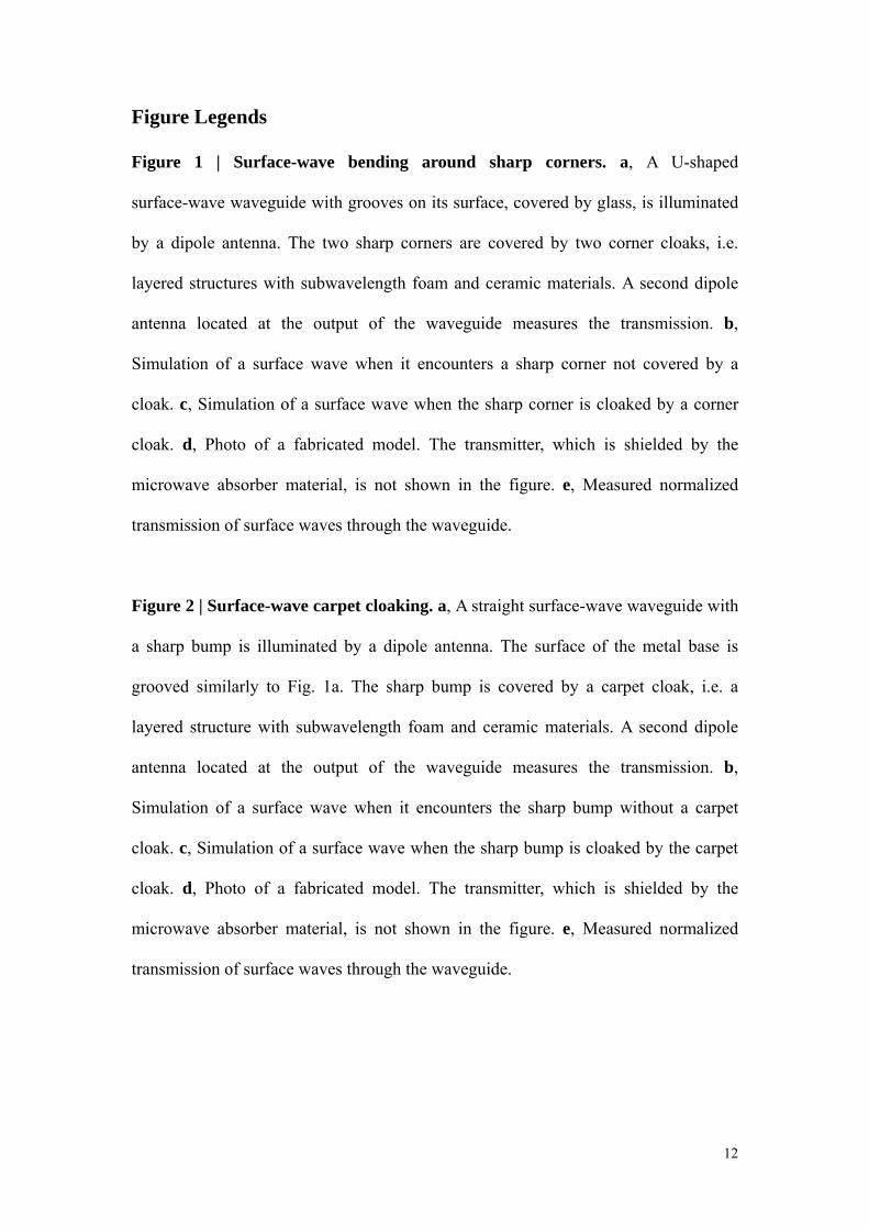
Figure 3 | A Gaussian-shaped pulse propagates on the patterned metal. A point
source (Port 1) generates the pulse at 0 ns. The bandwidth of the pulse is 6 GHz and
the center frequency is 3 GHz. The magnetic field distributions for three cases (the
corner cloaks (a), the carpet cloak (b), and the straight waveguide reference (c)) are
plotted to show the propagation of the pulse at five equivalent temporal sampling
points.
Figure 4 | Phase measurements. a, The corner cloaks. b, The carpet cloak. The
phases with the straight waveguide are plotted for reference. In both cases the phase
curves almost coincide with their references over the frequency band from 0+ to 6
GHz.

14
Figures
Figure 1
Figure 2
15
Figure 3
Figure 4

16
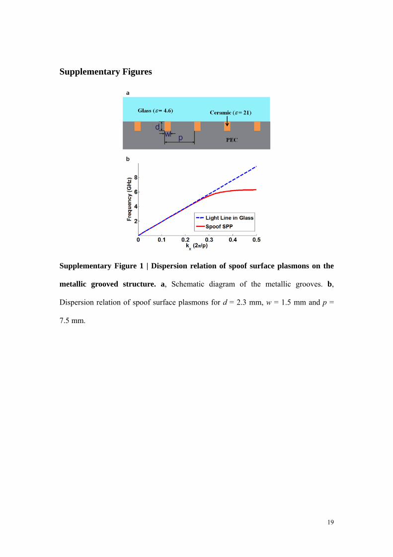
Supplementary Methods Dispersion relation of spoof surface plasmons on the metallic grooved structure
used in our models. Supplementary Fig. 1a shows the perfect electric conductor
(PEC) surface with a 1D periodic array of grooves with periodicity p. Each groove
has width w and depth d. All grooves are filled with a ceramic material with
permittivity ceramic= 21. The background material above the grooved structure is glass
with b= 4.6. Supplementary Fig. 1b shows the simulated dispersion relation of spoof
surface plasmons for d = 2.3 mm, w = 1.5 mm and p = 7.5 mm.
Specifications of the U-shaped waveguide and the corner cloaks. Here we briefly
introduce the transformation design. Supplementary Fig. 2a shows the
three-dimensional scheme of the U-shaped waveguide with sharp corners and periodic
grooves. The layered metamaterial structure is a stack of Rohacell® 71HF foam plates
(foam= 1.10; loss tangent 416 10 ; 1.06 mm thickness) and Wuxichaoying® K-21
microwave dielectric ceramic plates (ceramic= 21; loss tangent 1104 ; 1 mm
thickness). From the effective medium theory, the effective permittivities of the corner
cloaks can be obtained as 1 21 , 1ceramic foam ceramic foam ceramic foamr r r r ,
with the filling factor r 0.485.
The x-y projection in Supplementary Fig. 2a shows a feasible transformation of
the original EM space for EM surface waves propagating on a metal/dielectric
interface: the region MnOnAn (blue color)is transformed into MnOnA’n(red color), with
its area being preserved; symmetrically, the region WnOnVnis transformed into
WnOnV’n. The subscript n = 1 or 2 represents the nth 90°corner. Note that because the
surface EM waves have magnetic field along z direction, only the z-component of

17
permeability is relevant, which, according to the principle of transformation optics, is
equal to 1 / det( )z J , where det( )J is the Jacobian of the transformation. Since the
Jacobian represents the change of an infinitesimal area in the transformation, the area
preservation from MnOnAn to MnOnA’n and WnOnVn to WnOnV’n guarantees that 1z .
Thus we can implement a perfect full-parameter metamaterial corner cloak with
dielectric materials. For |AnOn|=50 mm, |AnMn|=75 mm, and |A’nOn|=42.4 mm, the
required principal permittivities of the corner cloaks are ε1=10.7 and ε2=2.0.
Supplementary Fig. 2b shows triangular pieces of the metamaterial structure. Four
identical triangles of the metamaterial structure form two corner cloaks that
effectively bend surface waves across the two right-angle zero-radius corners of the
U-shaped waveguide.
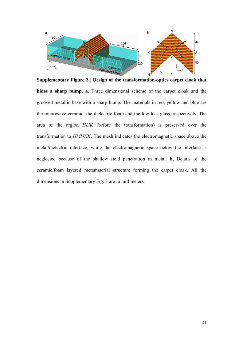
Specifications of the carpet cloak. Supplementary Fig. 3a illustrates the three
dimensional scheme of the carpet cloak and the grooved surface-wave waveguide
with a sharp bump. The carpet cloak is constructed with a layered metamaterial
structure composed of Wuxichaoying® K-21 microwave dielectric ceramic plates
(ceramic= 21; loss tangent 41 10 ; 1 mm thickness) and Rohacell® 71HF foam plates
(foam= 1.10; loss tangent 416 10 ; 1.06 mm thickness).
The x-y projection in Supplementary Fig. 3a shows the area-preserving
transformation for the carpet cloak. The original rectangular space HIJK (blue color)
is transformed into two symmetric and connected parallelograms HMNK and IMNJ
(red color), under the area-preservation constraint. The constitutive parameters of the
transformation medium are obtained with the same method used for the corner cloaks.
Because the area is invariant in the transformation, the permeability is intrinsically
unitary. For |HI| = 100 mm, |HM|=66.6 mm, and |HK| = 50 mm, the carpet cloak

18
requires the same metamaterial used for the corner cloaks. Supplementary Fig. 3b
shows details of the ceramic/foam layered metamaterial structure.
Supplementary Videos Supplementary Video 1 | A Gaussian-shaped pulse propagates on the patterned
metal with two zero-radius sharp corners. Upper left panel: When there is no cloak,
most pulse energy is scattered at the corners. Upper right panel: When two corners are
cloaked, the pulse can be perfectly guided around the two sharp corners. Lower panel:
A pulse propagates on a straight patterned metal as a reference.
Supplementary Video 2 | A Gaussian-shaped pulse propagates on the patterned
metal with a sharp bump. Upper panel: When there is no cloak, most pulse energy is
scattered at the bump. Middle panel: When the carpet cloak hides the bump, the pulse
can be perfectly guided around the bump. Lower panel: A pulse propagates on a
straight patterned metal as a reference.
19
Supplementary Figures
Supplementary Figure 1 | Dispersion relation of spoof surface plasmons on the
metallic grooved structure. a, Schematic diagram of the metallic grooves. b,
Dispersion relation of spoof surface plasmons for d = 2.3 mm, w = 1.5 mm and p =
7.5 mm.
20
Supplementary Figure 2 | Design of the transformation-optics corner cloaks for
sharp bending of electromagnetic surface waves. a, Three dimensional scheme of
the U-shaped surface-wave waveguide. The materials in red, yellow and blue are the
microwave ceramic, the dielectric foam, and the low-loss glass, respectively. The
areas of the regions n n nM O A and n n nW O V (before the transformation) are preserved
over the transformation to 'n n nM O A and '
n n nW O V respectively, where the subscript n
indicates the nth sharp corner. The mesh shows the electromagnetic space above the
metal/dielectric interface, while the electromagnetic space below the interface is
neglected because of the shallow field penetration in metal. b, Dimensions of the
ceramic/foam layered metamaterial structure. Four triangles of the metamaterial
structure form two corner cloaks. All the dimensions in Supplementary Fig. 2 are in
millimeters.
21
Supplementary Figure 3 | Design of the transformation-optics carpet cloak that
hides a sharp bump. a, Three dimensional scheme of the carpet cloak and the
grooved metallic base with a sharp bump. The materials in red, yellow and blue are
the microwave ceramic, the dielectric foam and the low-loss glass, respectively. The
area of the region HIJK (before the transformation) is preserved over the
transformation to HMIJNK. The mesh indicates the electromagnetic space above the
metal/dielectric interface, while the electromagnetic space below the interface is
neglected because of the shallow field penetration in metal. b, Details of the
ceramic/foam layered metamaterial structure forming the carpet cloak. All the
dimensions in Supplementary Fig. 3 are in millimeters.