broadband methodology for power distribution system analysis … · 2020-03-22 · designcon 2009...
TRANSCRIPT
DesignCon 2009
Broadband Methodology for
Power Distribution System
Analysis of Chip, Package and
Board for High Speed IO Design
Hsing-Chou Hsu, VIA Technologies
Jack Lin, Sigrity Inc.
Chi-Hsing Hsu, Azurewave Technologies

Abstract A broadband analysis methodology is described for the design of a power distribution
system (PDS) for high-speed IO, including chip, package and board. Rather than a
traditional time-domain simulation, the IO PDS is characterized through frequency
domain impedances, accounting for the PDS coupling that drives simultaneous switching
effects for adjacent IO cells. Chip-package-board co-simulation, what-if analysis and
decap optimization are implemented to produce a low PDS impedance response
throughout the system. This methodology has the advantages of greater insight for the
system-level influence of each domain as well as enabling resonance effects to be
avoided at critical system frequencies.
Author(s) Biography Hsing-Chou Hsu received his MSEE from National Chiao Tung University and is
currently a Signal Integrity manager at VIA Technologies. He has been responsible for
signal and power integrity analysis for high speed interfaces. He has developed extensive
experience in the design and characterization of the high-speed digital chipset
engineering and management positions in Taipei and Beijing. He has published 7
technical papers, gotten the recognition of 57th ECTC outstanding paper award, and
earned 15 patents, with some more pending.
Jack Lin received his Master degree from Physics Department of National Taiwan
University. He has over 10 years in SI/PI/EMC design experience for digital system
which includes chip, package and board in this industry. He is currently a Regional
Manager of Technical Support of Sigrity, Inc. Taiwan Branch Office.
Chi-Hsing Hsu received his MSME from National Tsing Hua University in 1996. He
worked for VIA Technologies as a package design manager from 2001 to 2007. He is
currently manager of Central Engineering Department at AzureWave Technologies. His
current interests cover a board range of electronic packaging and manufacturing
technology. He holds over 17 US patents and numerous international patents in the field
of electronic packaging.
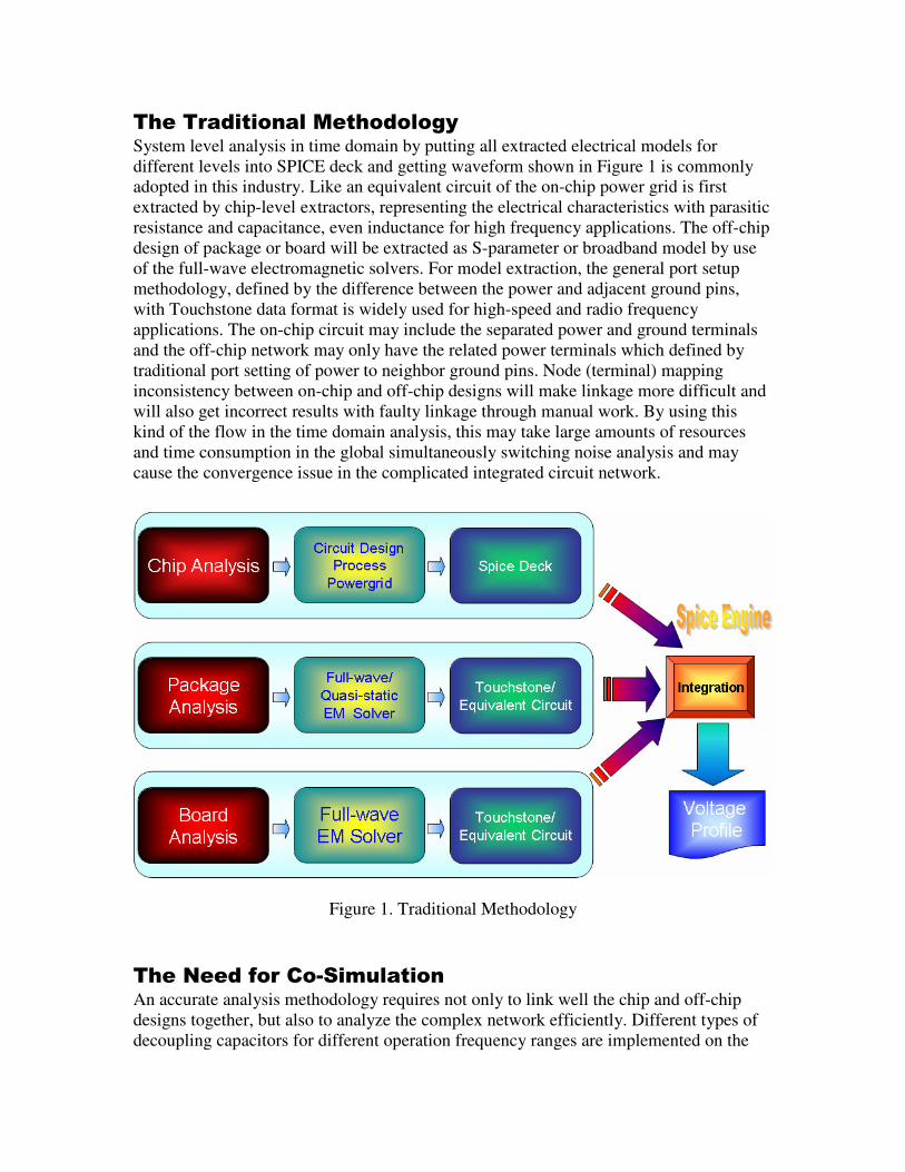
The Traditional Methodology System level analysis in time domain by putting all extracted electrical models for
different levels into SPICE deck and getting waveform shown in Figure 1 is commonly
adopted in this industry. Like an equivalent circuit of the on-chip power grid is first
extracted by chip-level extractors, representing the electrical characteristics with parasitic
resistance and capacitance, even inductance for high frequency applications. The off-chip
design of package or board will be extracted as S-parameter or broadband model by use
of the full-wave electromagnetic solvers. For model extraction, the general port setup
methodology, defined by the difference between the power and adjacent ground pins,
with Touchstone data format is widely used for high-speed and radio frequency
applications. The on-chip circuit may include the separated power and ground terminals
and the off-chip network may only have the related power terminals which defined by
traditional port setting of power to neighbor ground pins. Node (terminal) mapping
inconsistency between on-chip and off-chip designs will make linkage more difficult and
will also get incorrect results with faulty linkage through manual work. By using this
kind of the flow in the time domain analysis, this may take large amounts of resources
and time consumption in the global simultaneously switching noise analysis and may
cause the convergence issue in the complicated integrated circuit network.
Figure 1. Traditional Methodology
The Need for Co-Simulation An accurate analysis methodology requires not only to link well the chip and off-chip
designs together, but also to analyze the complex network efficiently. Different types of
decoupling capacitors for different operation frequency ranges are implemented on the

chip, package and board to maintain broadband low PDS impedance shown in Figure 2.
Most of the off-chip PDS acts have high impedance by inductive characteristic up to the
hundreds MHz. It is hard to improve PDS performance efficiently by using off-chip
capacitors once the operation frequency is higher than its self resonance [1-3]. The
interaction between the equivalent inductive effect of the off-chip power network and
capacitive one of the chip capacitor will produce high-impedance anti-resonance.
Eliminating anti-resonances induced by chip, package and board through decoupling
capacitor optimization on system level is an important task. Consequently, an efficient
and accurate way of co-simulation methodology is necessary to solve such complex
scenario for a low impedance and high performance PDS.
(a). Physical Decoupling Capacitor Arrangement
(b). Decoupling Capacitor Interaction
Figure 2. Power Distribution System Impedance Interaction
Proposed Co-simulation Methodology A new system-integrated PDS methodology is proposed in Figure 3 [4]. First, the
package is merged with the board and the combined system is characterized by hybrid 3D
EM solver, due to the complex physical structures with different kinds of decoupling
capacitors arrangement. Secondarily, by use of the chip-level extraction, the chip layout
GDSII file is imported as the analyze database and the die capacitors, implemented by
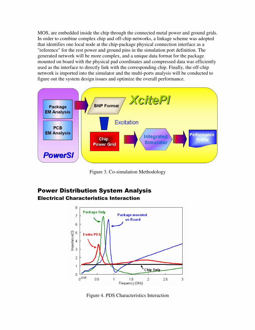
MOS, are embedded inside the chip through the connected metal power and ground grids.
In order to combine complex chip and off-chip networks, a linkage scheme was adopted
that identifies one local node at the chip-package physical connection interface as a
"reference" for the rest power and ground pins in the simulation port definition. The
generated network will be more complex, and a unique data format for the package
mounted on board with the physical pad coordinates and compressed data was efficiently
used as the interface to directly link with the corresponding chip. Finally, the off-chip
network is imported into the simulator and the multi-ports analysis will be conducted to
figure out the system design issues and optimize the overall performance.
Figure 3. Co-simulation Methodology
Power Distribution System Analysis
Electrical Characteristics Interaction
Figure 4. PDS Characteristics Interaction
A high performance PDS design must avoid resonances within the operation frequency
bandwidth for the power stability consideration. How to well predict and eliminate the
resonances due to interactions among different domains is a design challenge. Figure 4
shows the electrical characteristics interaction among chip, package and board. The
resonance of the analyzed flip chip package, designed with decoupling capacitors to
reduce its PDS impedance, occurs at 700MHz for the parallel plates between
power/ground pairs. Once the package is mounted on the board, the resonance is pushed
to higher frequency at 850MHz due to the effective inductance reduction by the
additional return current path through the board connection. After chip connecting with
off chip networks, the resonance of the entire PDS is shifted to the lower frequency at
550MHz by the interaction between the on-chip capacitive and off-chip inductive
characteristics.
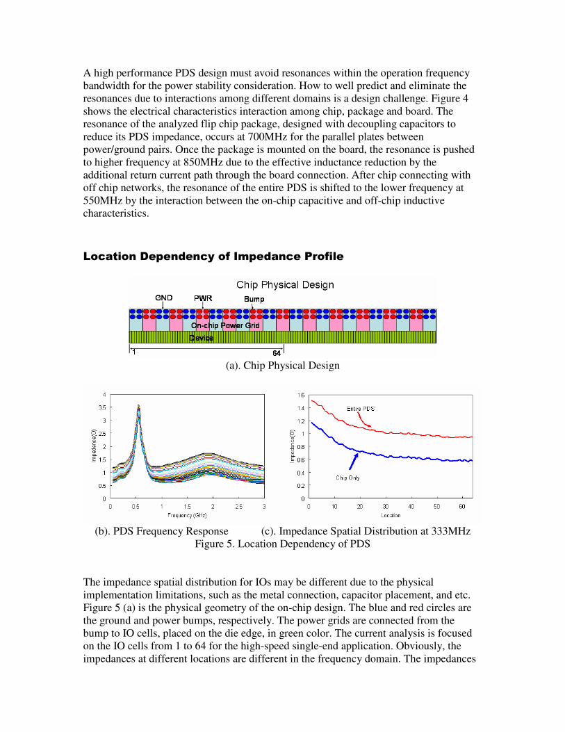
Location Dependency of Impedance Profile
(a). Chip Physical Design
(b). PDS Frequency Response (c). Impedance Spatial Distribution at 333MHz
Figure 5. Location Dependency of PDS
The impedance spatial distribution for IOs may be different due to the physical
implementation limitations, such as the metal connection, capacitor placement, and etc.
Figure 5 (a) is the physical geometry of the on-chip design. The blue and red circles are
the ground and power bumps, respectively. The power grids are connected from the
bump to IO cells, placed on the die edge, in green color. The current analysis is focused
on the IO cells from 1 to 64 for the high-speed single-end application. Obviously, the
impedances at different locations are different in the frequency domain. The impedances
monitored at the fundamental frequency of 333MHz for the major operation in Figure 5(c)
were recorded to figure out the power integrity of different I/O circuit blocks. The
impedance of the entire PDS from different I/O devices is different and larger than the
chip only case because of the added effective inductance from the off-chip power
network. The impedance of the corner devices, compared with the rest ones, is larger due
to the unbalanced power grid design. This kind of the analysis is beneficial to arrange the
critical signals properly in the power integrity perspective.
Power Distribution System Interference
The total impedance, including the self input impedance and mutual ones from the other
active IOs, is proposed to capture the simultaneous switching noise (SSN) in frequency
domain perspective, instead of the time domain. Such impedance analysis in frequency
domain is not only an efficient way but also revealing of PDS problems in depth, like
PDS interference by the shared current path.
Compared to the input PDS impedance, the total impedance profile in the worst case
scenario significantly increased more than thirty times (30X) in the broadband frequency,
especially when there is a high increment at the resonant frequency. The transfer
impedance coupling decreased as the distance between the victim and aggressor
increased. The ratio of the decay and accumulation in PDS were used to evaluate PDS
interference and the total impedance influenced by SSN.
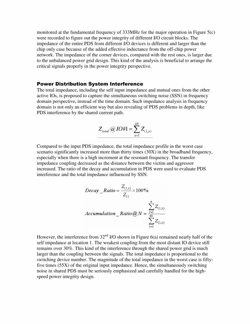
However, the interference from 32nd
I/O shown in Figure 6(a) remained nearly half of the
self impedance at location 1. The weakest coupling from the most distant IO device still
remains over 30%. This kind of the interference through the shared power grid is much
larger than the coupling between the signals. The total impedance is proportional to the
switching device number. The magnitude of the total impedance in the worst case is fifty-
five times (55X) of the original input impedance. Hence, the simultaneously switching
noise in shared PDS must be seriously emphasized and carefully handled for the high-
speed power integrity design.
(a). PDS Interference (b). Decay and Accumulation Ratios
(c). Frequency Response of Self and Total Impedance
Figure 6. PDS Interference
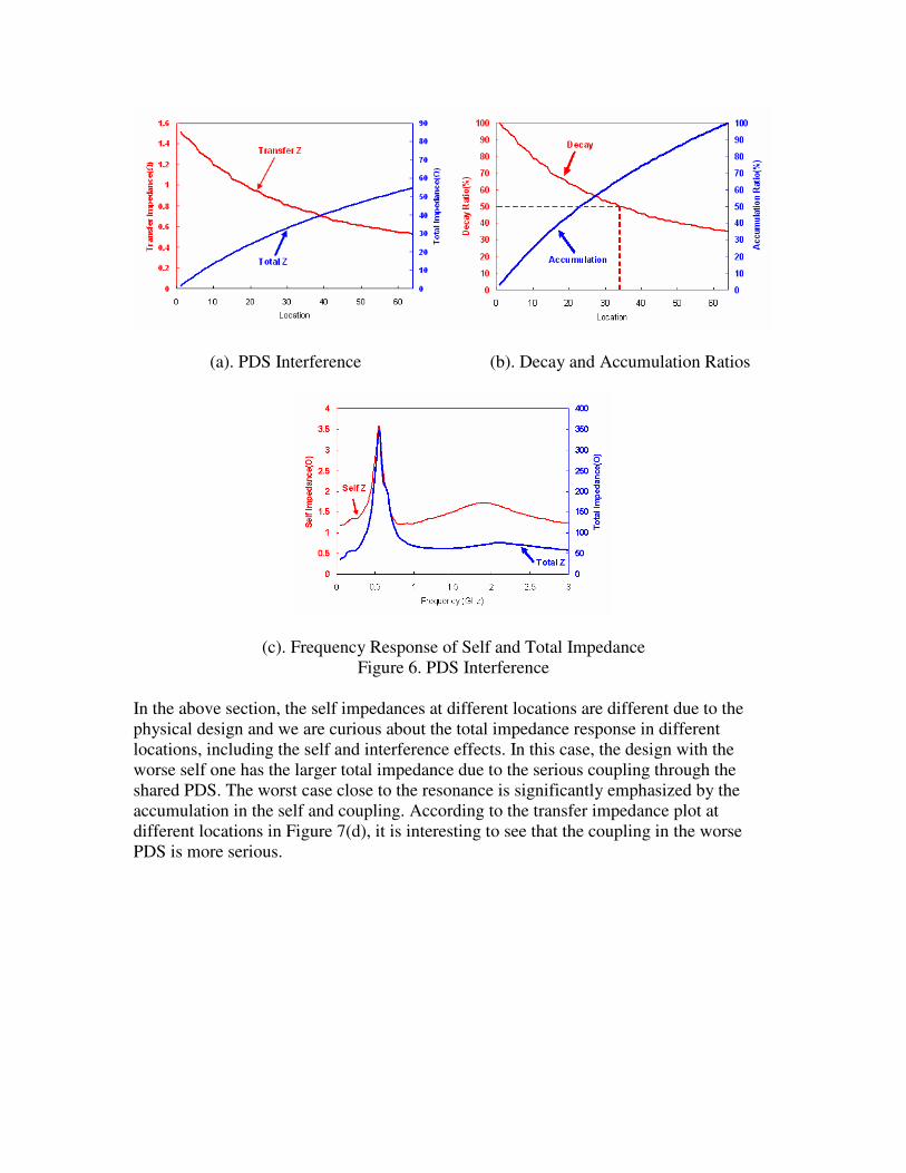
In the above section, the self impedances at different locations are different due to the
physical design and we are curious about the total impedance response in different
locations, including the self and interference effects. In this case, the design with the
worse self one has the larger total impedance due to the serious coupling through the
shared PDS. The worst case close to the resonance is significantly emphasized by the
accumulation in the self and coupling. According to the transfer impedance plot at
different locations in Figure 7(d), it is interesting to see that the coupling in the worse
PDS is more serious.
(a). Self Impedance (b). Total Impedance
(c). Self and Total Impedance at 333MHz (d). Transfer Impedance
Figure 7. PDS Interference
What-if Analysis in Decoupling Capacitors Population
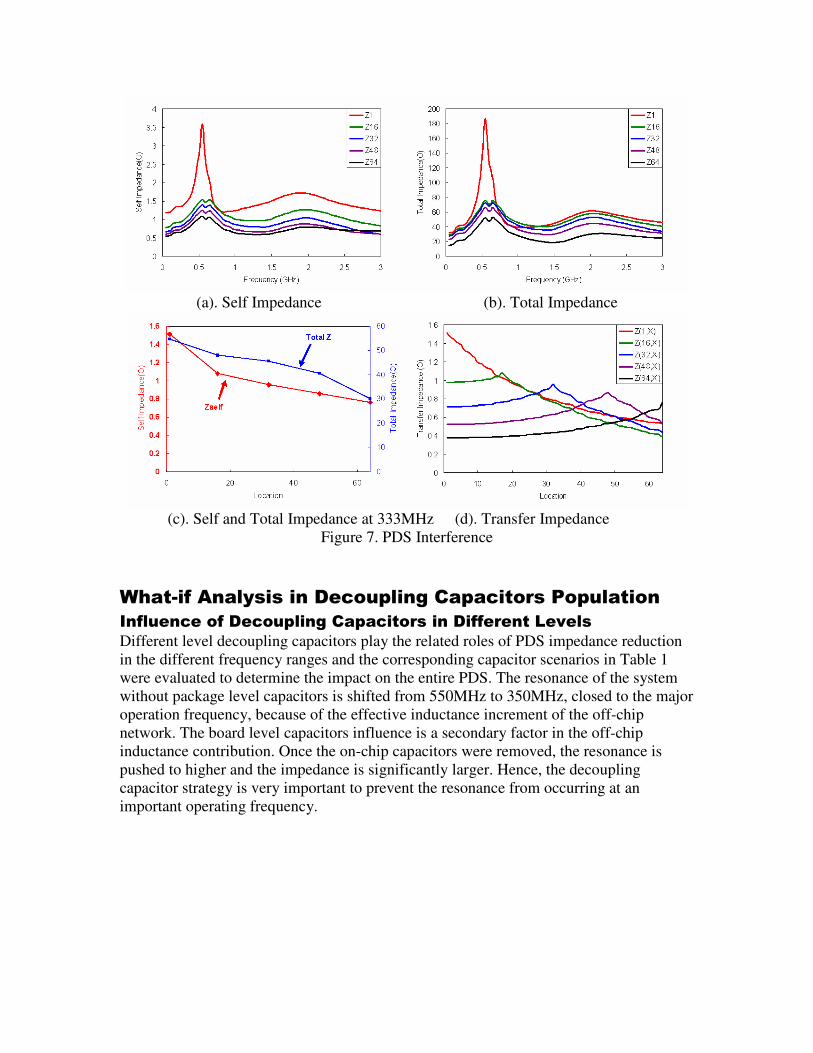
Influence of Decoupling Capacitors in Different Levels
Different level decoupling capacitors play the related roles of PDS impedance reduction
in the different frequency ranges and the corresponding capacitor scenarios in Table 1
were evaluated to determine the impact on the entire PDS. The resonance of the system
without package level capacitors is shifted from 550MHz to 350MHz, closed to the major
operation frequency, because of the effective inductance increment of the off-chip
network. The board level capacitors influence is a secondary factor in the off-chip
inductance contribution. Once the on-chip capacitors were removed, the resonance is
pushed to higher and the impedance is significantly larger. Hence, the decoupling
capacitor strategy is very important to prevent the resonance from occurring at an
important operating frequency.
Table 1. Decoupling Capacitor Scenario in Different Physical Levels
Figure 8. PDS Frequency Response of Different Capacitor Scenario
On-chip Capacitor Impact on the Entire PDS
On-chip capacitors are most beneficial to the high frequency PDS impedance reduction
by the immediate charge tank with the lowest parasitic inductance, compared with the
off-chip ones. The different scenarios with different on-chip capacitors were evaluated to
determine the impact on PDS impedance. Due to the interaction between the on-chip
capacitor and off-chip effective inductance, an expected anti-resonance will be induced to
degrade the mid-frequency power integrity. Once the design excluded the on-chip
capacitor implementation, the resonance is shifted to higher frequency for the specific
application but the PDS impedance is becoming much worse up to 1GHz. The larger on-
chip capacitor, the lower frequency the resonance is and the entire PDS impedance
profile is reduced.
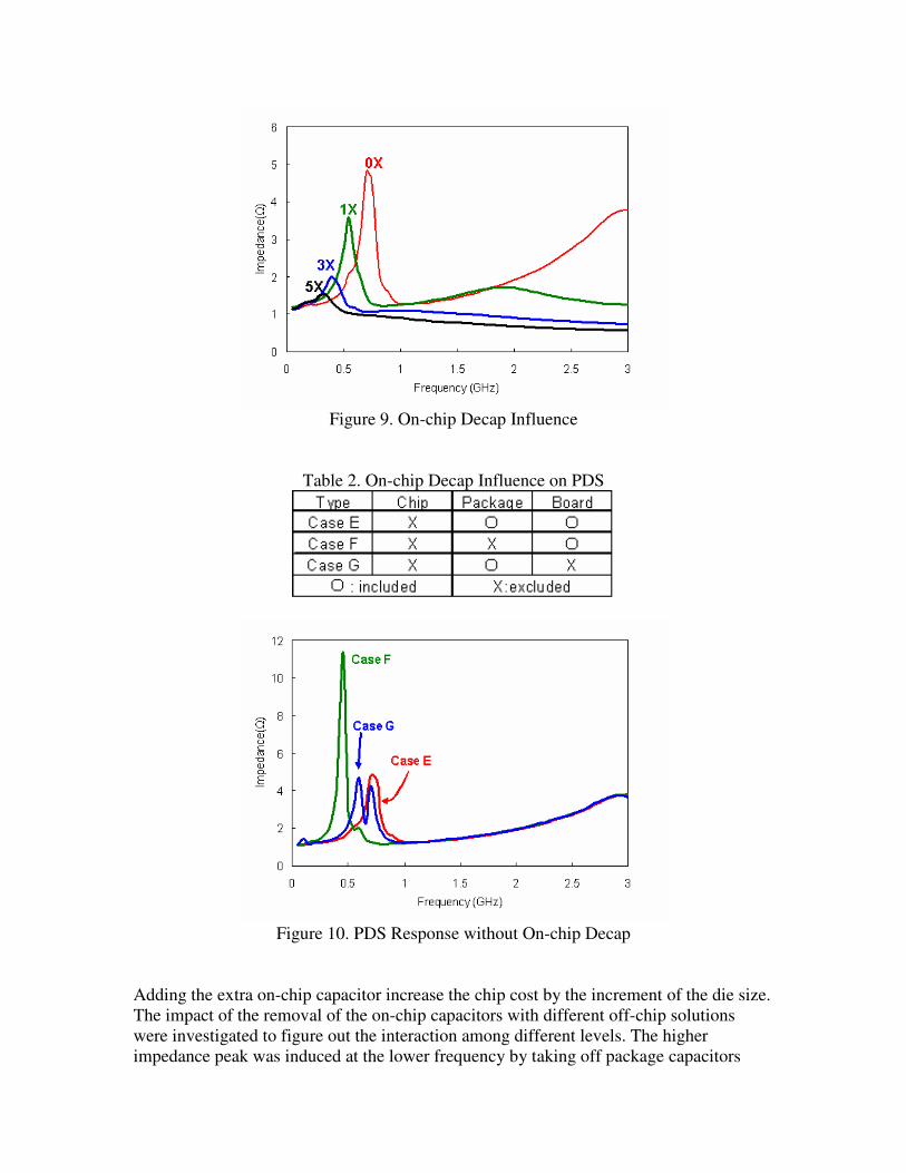
Figure 9. On-chip Decap Influence
Table 2. On-chip Decap Influence on PDS
Figure 10. PDS Response without On-chip Decap
Adding the extra on-chip capacitor increase the chip cost by the increment of the die size.
The impact of the removal of the on-chip capacitors with different off-chip solutions
were investigated to figure out the interaction among different levels. The higher
impedance peak was induced at the lower frequency by taking off package capacitors
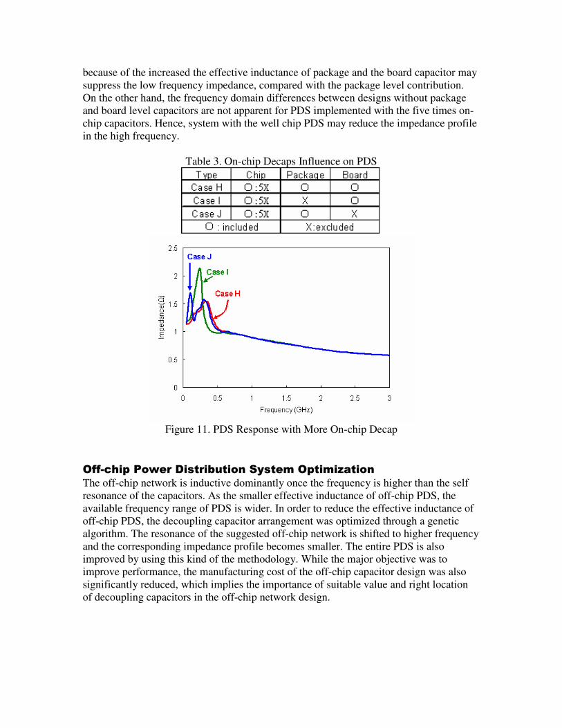
because of the increased the effective inductance of package and the board capacitor may
suppress the low frequency impedance, compared with the package level contribution.
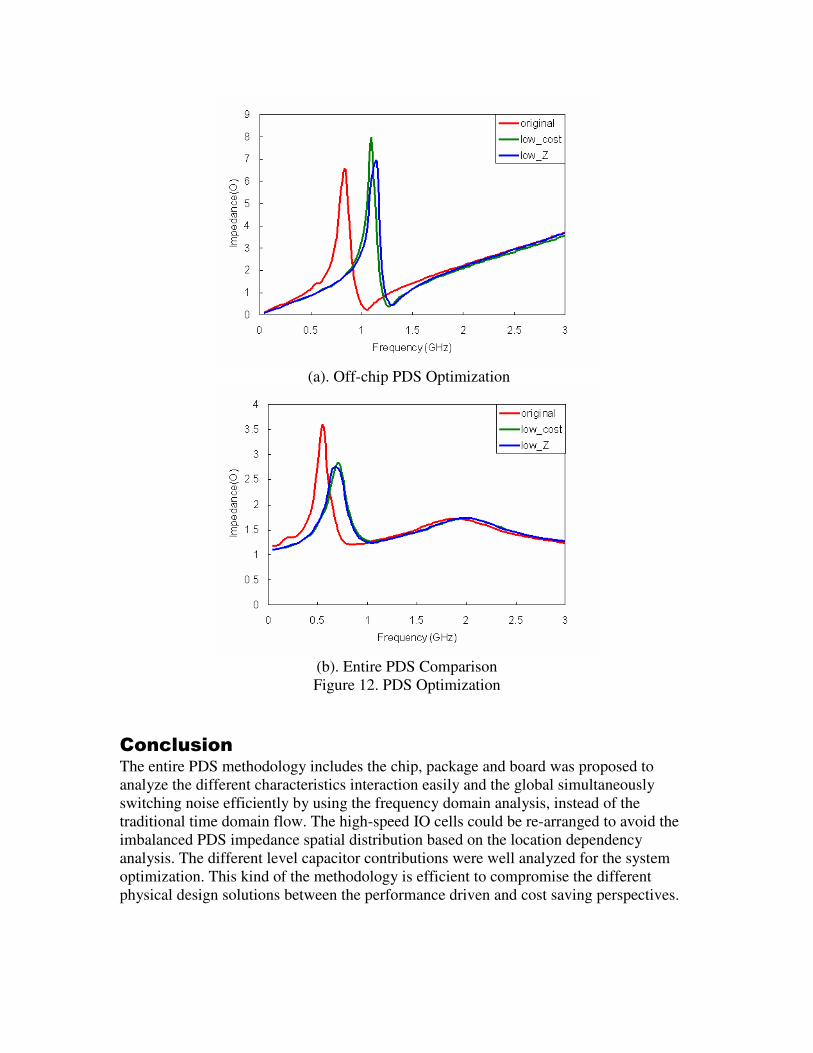
On the other hand, the frequency domain differences between designs without package
and board level capacitors are not apparent for PDS implemented with the five times on-
chip capacitors. Hence, system with the well chip PDS may reduce the impedance profile
in the high frequency.
Table 3. On-chip Decaps Influence on PDS
Figure 11. PDS Response with More On-chip Decap
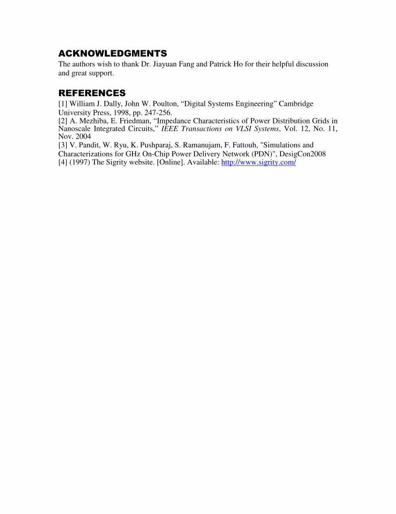
Off-chip Power Distribution System Optimization
The off-chip network is inductive dominantly once the frequency is higher than the self
resonance of the capacitors. As the smaller effective inductance of off-chip PDS, the
available frequency range of PDS is wider. In order to reduce the effective inductance of
off-chip PDS, the decoupling capacitor arrangement was optimized through a genetic
algorithm. The resonance of the suggested off-chip network is shifted to higher frequency
and the corresponding impedance profile becomes smaller. The entire PDS is also
improved by using this kind of the methodology. While the major objective was to
improve performance, the manufacturing cost of the off-chip capacitor design was also
significantly reduced, which implies the importance of suitable value and right location
of decoupling capacitors in the off-chip network design.
(a). Off-chip PDS Optimization
(b). Entire PDS Comparison
Figure 12. PDS Optimization
Conclusion The entire PDS methodology includes the chip, package and board was proposed to
analyze the different characteristics interaction easily and the global simultaneously
switching noise efficiently by using the frequency domain analysis, instead of the
traditional time domain flow. The high-speed IO cells could be re-arranged to avoid the
imbalanced PDS impedance spatial distribution based on the location dependency
analysis. The different level capacitor contributions were well analyzed for the system
optimization. This kind of the methodology is efficient to compromise the different
physical design solutions between the performance driven and cost saving perspectives.
ACKNOWLEDGMENTS The authors wish to thank Dr. Jiayuan Fang and Patrick Ho for their helpful discussion
and great support.
REFERENCES
[1] William J. Dally, John W. Poulton, “Digital Systems Engineering” Cambridge
University Press, 1998, pp. 247-256. [2] A. Mezhiba, E. Friedman, “Impedance Characteristics of Power Distribution Grids in Nanoscale Integrated Circuits,” IEEE Transactions on VLSI Systems, Vol. 12, No. 11, Nov. 2004 [3] V. Pandit, W. Ryu, K. Pushparaj, S. Ramanujam, F. Fattouh, "Simulations and
Characterizations for GHz On-Chip Power Delivery Network (PDN)", DesigCon2008 [4] (1997) The Sigrity website. [Online]. Available: http://www.sigrity.com/