board level reliability of chip scale packages - imaps · board level reliability of chip scale...
TRANSCRIPT

© International Microelectronics And Packaging Society
The International Journal of Microcircuits and Electronic Packaging, Volume 23, Number1, First Quarter 2000 (ISSN 1063-1674)
Intl. Journal of Microcircuits and Electronic Packaging
118
Board Level Reliability of Chip Scale PackagesS.C. Hung, P.J. Zheng, H.N. Chen, S.C. Lee, and J.J. LeeAdvanced Semiconductor Engineering, (ASE), Inc.26, Chin 3rd Rd., 811Nantze Export Processing ZoneKaohsiung, TaiwanPhone: 886-7-3617131 ext. 5210Fax: 886-7-3613094e-mail: [email protected]
Abstract
The joint fatigue life of PBGA, TFBGA, Film BGA, micro-BGA and BCC/BCC++ is studied in this work. The effects of temperatureprofile, joint standoff, polyimide thickness, epoxy thickness, test board surface finish, and solder paste composition on the fatigue lifeare investigated. The temperature ramp rate has significant effect on the joint fatigue life. Attention should be paid not to reach thelevel of thermal shock. The effect of joint standoff can be predicted by shear strain energy density in the joint. The effect of polyimidethickness on the joint fatigue life is found to be more significant than does die paste thickness. The surface finish of test board alsoinfluences the fatigue life, although the difference between OSP and HASL is not significant. A 2% silver additive in the eutecticsolder paste improves joint fatigue life. Different pad configurations induce different levels of stress concentration, and thus causedifferent levels of damage. This effect is found the same for both rigid- and flex-BGA. DNP effect is found to be very insignificant forboth TF and Film BGA. However, the die edge effect is demonstrated to be tremendous. This can be due to the stress concentrationand warpage near the edges of the chip caused by local CTE mismatch and the changes in flexural rigidity. Surface finish of testboard affects the formation and the type of IMC. Different IMC affects joint fatigue life differently and cause different failure modes.
Key words:
Chip Scale Package, Film BGA, TFBGA, Micro-BGA, BCC,Fatigue Life, and Reliability.
1. Introduction
As portable electronic devices have become smaller, thinner,lighter, and more powerful in the recent years, the request ofchip scale packages has become extremely high. However, sincethe packages have the characteristics of small and thin outline,and thus fine pitch and high density, the standoff of the solderinterconnects becomes lower, the compliance of the solder jointsdegrades. Furthermore, the volume fraction of the chip in chipscale packages becomes larger, hence intensifies the thermalmismatch between the package and the motherboard. As a re-sult, the fatigue life of the solder joint interconnection is under a
great impact due to the smaller pad size, lower standoff height,and greater thermal mismatch. Therefore, the second level reli-ability becomes a key issue for chip scale packages.
Recently, sizable efforts have been devoted to investigate theboard level reliability of chip scale packages1-16. The fatigue lifeof a wide variety of CSP was reported1-6. The works cover a widerange of package types including rigid substrate CSP1-3, flex sub-strate CSP1, 4-5, lead-frame CSP1 and wafer level CSP6. The otherattempt in predicting joint fatigue life is by evaluating the ther-mal stress induced in solder joint using numerical models3, 7-10.Using Finite Element modeling, the package design can be opti-mized prior to package prototyping, however, the drawback isthe verification and the validation of these models. Furthermore,process-related factors are difficult to be included into these mod-els. Key factors affecting joint reliability were investigated anddiscussed extensively5, 11-20 for various Chip Scale packages. Thefactors investigated include die size5, 11, 19-20, pad design11, 19-20, diepaste11, solder shape13, solder composition11, underfill11, 13, boardthickness5, 19-20, and surface finish of test board15-17. As more chipscale packages are to be used in telecommunication products, thejoint reliability under mechanical tests such as bend6, 21-22 anddrop13 tests are gaining popularity. More recently, a work to dis-cuss field and accelerated test conditions has been reported and

Board Level Reliability of Chip Scale Packages
The International Journal of Microcircuits and Electronic Packaging, Volume 23, Number1, First Quarter 2000 (ISSN 1063-1674)
© International Microelectronics And Packaging Society 119
raised a question whether solder joints have been over-designed23.Since assurance of board level reliability of a package is es-
sential for applying it into products, this work investigates jointreliability of several chip scale packages under thermal cyclictest. The packages are TFBGA (thin and fine pitch), Film BGA,micro-BGA, and bump chip carrier (BCC/BCC++). A smallPBGA is also tested as a benchmark. Both of the TFBGA andFilm BGA have a die-up, wirebonded and over-molded configu-ration. TFBGA uses a BT substrate, while Film BGA uses apolyimide substrate. Since the size of TFBGA is only 8mmx9mmwith 1.1mm mounting height and 0.75mm ball pitch, it becomesa suitable candidate for flash memory SRAM, ROM, RAM andASIC. Film BGA has a size of 12mmx12mmx1.1mm and has132 solder balls with 0.8mm ball pitch. It uses polyimide as asubstrate to enhance its electrical and thermal performance. Asa result, it is suitable for ASIC, DSP, flash and portable equip-ment such as cellular phone, digital camera, and digital tape re-corder. The size of micro-BGA is 7.8mmx5.8mm with a mount-ing height of 0.93mm and 0.75mm ball pitch. Its application isaimed at DRAM and flash memory. As for bump chip carrier,normal BCC has a size of 7mmx7mm and 48 terminals. BCC++has extra ground wires and an extra cavity, which connects to themotherboard after surface mount. Therefore, its electrical andthermal performance is enhanced. Its size is 9mmx9mm with 64terminals. Both of BCC and BCC++ have 0.8mm mountingheight and 0.5mm ball pitch. Their main application is fortelecommunication products.
2. Test Vehicles and ExperimentalMatrix
In this work, the PBGA test vehicle is used to study the effectof temperature profile on the fatigue life and also the die edgeeffect on the failure location. Two different sizes of solder ballswere used for TFBGA, and therefore the effect of joint standoffon the fatigue life is obtained. For the Film BGA, four types ofspecimens were prepared to probe the effects of epoxy thickness;polyimide thickness and test board surface finish on the jointfatigue life. The package profile, die size, and ball matrix ofTFBGA, Film BGA, and PBGA are shown in Figure 1. Formicro-BGA and BCC/BCC++, the main goals are to probe thejoint fatigue life and the corresponding failure modes under tem-perature cyclic test due to their special and unique configura-tions. The cross sections of BCC/BCC++ and micro-BGA areillustrated in Figures 2 and 3, respectively. Also, the packageoutline dimensions of each test vehicle conducted are summa-rized in Table 1. Sample size, package parameters, and test boardthickness/surface finish are all listed in Table 2.
Figure 1. The outline and ball matrix of test vehicles.
Figure 2. The cross sections of BCC and BCC++.
Figure 3. The cross section of micro-BGA.
Table 1. Package profiles.
Package Size(mm)
Mountingheight (mm)
Ball pitch(mm)
Leads
TFBGA 8x9 1.1 0.8 48Film BGA 12x12 1.1 0.8 132
µBGA 7.8x5.8 1.0 0.75 46BCC 9x9 0.8 0.5 64BCC 7x7 0.8 0.5 48
PBGA 15x15 1.61 1.0 196

© International Microelectronics And Packaging Society
The International Journal of Microcircuits and Electronic Packaging, Volume 23, Number1, First Quarter 2000 (ISSN 1063-1674)
Intl. Journal of Microcircuits and Electronic Packaging
120
Table 2. Parameters of test vehicles.
A B C D E F G H IPackage
TF Film Film Film Film µBGA BCC++ BCCPBG
ASamples 30 15 15 15 15 15 30 15 75
Boardthickness
(mm)1.6 0.8 0.8 0.8 0.8 1.6 1.6 1.6 1.6
Pad finish Ni/Au HASL OSP OSP OSP HASL HASL HASL Ni/AuDie size
(mm)4.5x4.
79.0 9.0 9.0 9.0 5.8x7.9 5.3x7.1 4.57 8
Epoxythickness
(µm)25 75 75 25 25 NA 12.5 12.5 25
Ball size(mm)
0.3/0.4
0.45 0.45 0.45 0.45 0.30 NA NA 0.5
Au thickness(µm)
0.5 0.5 0.5 0.5 0.5 1.0 0.03 0.03 0.75
Polyimidethickness (µm)
NA 75 75 75 50 NA NA NA NA
3. Experimental Procedures
The procedure of the preparation of test vehicles and experi-mental setup is described in this section. For each of the testvehicles under investigation, a specific test board is designed.Test board is made of FR-4 and is designed to carry 15 test ve-hicles simultaneously. The test board has a size of220mmx139mm with a thickness of either 0.8mm or 1.6mm.The packages under investigation were then assembled using daisysubstrates. After package assembly was completed, the packageswere baked at 125°C for 24 hours to remove any potential mois-ture inside the packages. At this point, the test vehicles are readyto be mounted onto the test boards. The procedure of surfacemounting is described next. Solder paste was first printed ontotest boards, and packages were then mounted onto test boards bythe assistance of a fine-pitch pick and place machine. X-rayinspection was performed to ensure that all samples are locatedat exactly the right positions. Finally, all the test vehicles wentthrough a ten-zone, nitrogen-inert, forced-convention oven forreflow process. The peak temperature of reflow is 220±10°C.
After the packages were surface-mounted onto the test boards,the electrical circuit formed by daisy substrate and test board wasexamined to assure a good connection of all solder joints, thenall the test units were put into a temperature chamber for cyclictesting. Since solder joints of a test unit are daisy-chain con-nected, a real-time resistance measurement is implemented. Thetest system includes a control unit, a chamber, and a data acqui-sition system. The system is capable of measuring real-time in-situ electrical resistance of each and every test unit and also re-cording the corresponding temperature. In the measurement ofresistance, four-point probe is applied instead of two-terminalconfiguration to remove any effect (error) from connectors andwires. Failure criterion is defined as resistance reaches 300 ohms.
The two temperature profiles used in this work are shown inFigures 4 and 5. Each Figure contains prescribed and measuredtemperature profiles. From these Figures, it can be seen that the
measured temperature profiles follow the prescribed ones rea-sonably well. Figure 6 shows a typical resistance measurementof a daisy-chain unit (test vehicle). The resistance of a unit isinitially low and stable for most of the cycles that it is subject toand then becomes higher prior to solder joint failure. The varia-tion of the resistance prior to failure is believed to be caused bythe initiation, propagation, and resting of cracks during the tem-perature cyclic test. The test is stopped after all units on the sametest board fail. The recorded failure cycles were used to generateWeibull plots and parts were then subject to failure analysis.
-60
-30
0
30
60
90
120
150
15 30 45 60 75 90 105 120 135 150
Time (min)
Tem
p. (
C)
Monitor Setting
Figure 4. Temperature profile I.
-40-20
0
20406080
100120140
0 20 40 60 80 100 120 140
Time (min)
Tem
p.(
C) Measured
Prescribed
Figure 5. Temperature profile II.

Board Level Reliability of Chip Scale Packages
The International Journal of Microcircuits and Electronic Packaging, Volume 23, Number1, First Quarter 2000 (ISSN 1063-1674)
© International Microelectronics And Packaging Society 121
0
50
100
150
200
250
300
0 300 600 900 1200 1500
Cycle
Res
ista
nce
(ohm
)
Figure 6. A typical resistance measurement.
4. Fatigue Life of Solder Joints
In this section, fatigue life obtained of each test vehicle is re-ported. The effects of temperature profile, joint standoff, polyimidethickness, epoxy thickness, test board surface finish, and solderpaste composition on the joint fatigue life are discussed and com-pared.
4.1. Temperature Profile Effect
Two temperature profiles were used to study their effect onthe joint fatigue life. Both of these two profiles have the samefrequency of one cycle per hour (cph). However, the ramp-uptime, the dwell time at the highest temperature, the ramp-downtime, and the dwell time at the lowest temperature are 15, 15, 15and 15 minutes, respectively, for the first profile, and 5, 25, 5 and25 minutes, respectively, for the second profile. The temperaturerange for the first profile is from –40 to 125°C, while the secondone is from -25 to 125°C. Therefore, during transition periods,the temperature ramp rates are 11 and 30°C per minute for thefirst and second profiles, respectively. Both temperature profileshave been shown in Figures 4 and 5.
The PBGA test vehicles were used for this study. The Weibullplots of the joints tested under these two conditions are shown inFigure 7. The characteristic fatigue life of the solder intercon-nect is 1482 and 755 cycles, respectively, for the first, and thesecond temperature profiles. It was found that the characteristicfatigue life of solder joints under the first temperature profile is1.96 times of that under the second one. Although the tempera-ture variation (∆T) of the first profile is bigger than the secondone, the ramp rate and the dwell time of the second one are bothseverer than the first one. The ramp rate of the first profile is11°C/min, while it is 30°C/min for the second one. According tothe specification of IPC-SM-785, the maximum ramp rate is de-
fined as 20°C/min for thermal cyclic test. Furthermore, a ramp rateof 30°C/min reaches the level of thermal shock by specificationdefinition. Since thermal shock introduces cracks at much earlierstage and, the longer dwell time introduces and accumulates morecreep and stress-relaxation-enhanced damage to solder joints,therefore, the joint fatigue life under the second temperature pro-file is only 51% of the joint fatigue life under the first temperatureprofile.
0
0.2
0.4
0.6
0.8
1
400 900 1400 1900 2400
CyclesP
erce
nt f
aile
d
-25~125'C
-40~125'C
755 1482
63.2%
1.96X
Figure 7. The effect of temperature profile on joint fatiguelife.
4.2. Joint Standoff Effect
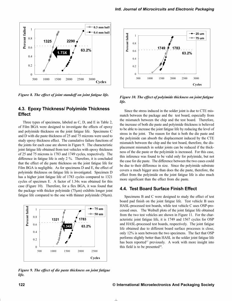
TFBGA is used to carry out this effect. Two sizes of solderballs were applied, which are 0.3mm and 0.4 mm. The firstfailure occurs at 885 and 1716 cycles, respectively, for the twojoint standoffs. Again, the characteristic joint fatigue life is 1325and 2290 cycles for 0.3mm and 0.4mm solder balls, respectively.From Figure 8, a factor of 1.73x is obtained. Since the onlydifference between the two test vehicles is the joint standoff, theshear strain induced in the joint by the CTE mismatch betweenthe package and the test board is inversely proportional to thestandoff. As a result, the strain energy density in 0.3mm ball isabout 1.78 (square of 0.4/0.3) times of that in 0.4mm ball. Sincethe fatigue life is approximately inversely proportional to the strainenergy density (Coffin-Mason equation), the fatigue life of 0.4mmball can then be expected to be 1.78 times of the fatigue life of0.3mm ball. Since the ratio obtained from experimental result is1.73, it can be concluded that the experimental result matchesthe simulated prediction very well.
© International Microelectronics And Packaging Society
The International Journal of Microcircuits and Electronic Packaging, Volume 23, Number1, First Quarter 2000 (ISSN 1063-1674)
Intl. Journal of Microcircuits and Electronic Packaging
122
0
0.2
0.4
0.6
0.8
1
500 1000 1500 2000 2500 3000Cycles
Per
cent
fai
led 0.3 mm ball
0.4 mm ball
1325 2290
63.2%1.73X
Figure 8. The effect of joint standoff on joint fatigue life.
4.3. Epoxy Thickness/ Polyimide ThicknessEffect
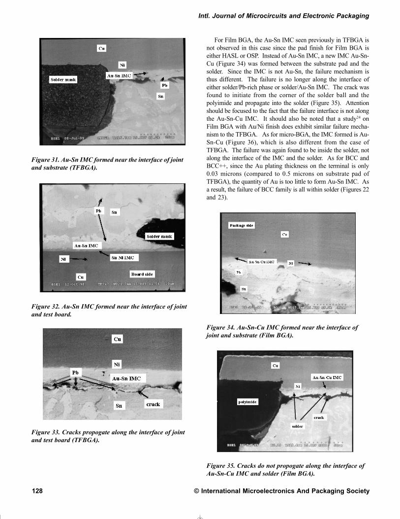
Three types of specimens, labeled as C, D, and E in Table 2,of Film BGA were designed to investigate the effects of epoxyand polyimide thickness on the joint fatigue life. Specimens Cand D with die paste thickness of 25 and 75 microns were used tostudy epoxy thickness effect. The cumulative failure functions ofthe joints for each case are shown in Figure 9. The characteristicjoint fatigue life obtained from test vehicles with epoxy thicknessof 25 and 75 microns is 1783 and 1749 cycles, respectively. Thedifference in fatigue life is only 2 %. Therefore, it is concludedthat the effect of die paste thickness on the joint fatigue life forFilm BGA is negligible. As for specimens D and E, the effect ofpolyimide thickness on fatigue life is investigated. Specimen Dhas a higher joint fatigue life of 1783 cycles compared to 1321cycles of specimen E. A factor of 1.34x was obtained for thiscase (Figure 10). Therefore, for a flex BGA, it was found thatthe package with thicker polyimide (75µm) exhibits longer jointfatigue life compared to the one with thinner polyimide (50µm).
0
0.2
0.4
0.6
0.8
1
500 1000 1500 2000 2500
Cycles
Per
cent
fai
led
75 um
50 um
1321 1783
63.2%1.34X
Figure 9. The effect of die paste thickness on joint fatiguelife.
0
0.2
0.4
0.6
0.8
1
500 1000 1500 2000 2500 3000
Cycles
Per
cent
fai
led 25 um
75 um
1749 1783
63.2%
Figure 10. The effect of polyimide thickness on joint fatiguelife.
Since the stress induced in the solder joint is due to CTE mis-match between the package and the test board, especially fromthe mismatch between the chip and the test board. Therefore,the increase of both die paste and polyimide thickness is believedto be able to increase the joint fatigue life by reducing the level ofstress in the joint. The reason for that is both the die paste andthe polyimide can absorb the displacement induced by the CTEmismatch between the chip and the test board, therefore, the dis-placement mismatch in solder joints can be reduced if the thick-ness of the die paste or the polyimide is increased. For this case,this inference was found to be valid only for polyimide, but notthe case for die paste. The difference between the two cases couldbe due to their difference in size. Since the polyimide substratecovers a much bigger area than does the die paste, therefore, theeffect from the polyimide on the joint fatigue life is also muchmore significant than the effect from die paste.
4.4. Test Board Surface Finish Effect
Specimens B and C were designed to study the effect of testboard pad finish on the joint fatigue life. Test vehicle B usesHASL-processed test boards, while test vehicle C uses OSP-pro-cessed ones. The Weibull plots of the joint fatigue life obtainedfrom the two test vehicles are shown in Figure 11. For the char-acteristic joint fatigue life, it is 1749 and 1567 cycles for OSPand HASL-processed test boards, respectively. The joint fatiguelife obtained due to different board surface processes is close,only 12% is seen between the two specimens. The fact that OSPperforms slightly better than HASL in the solder joint fatigue lifehas been reported17 previously. A work with more insight intothis field is to be presented24.

Board Level Reliability of Chip Scale Packages
The International Journal of Microcircuits and Electronic Packaging, Volume 23, Number1, First Quarter 2000 (ISSN 1063-1674)
© International Microelectronics And Packaging Society 123
0
0.2
0.4
0.6
0.8
1
500 1000 1500 2000 2500
Cycles
Per
cen
t fa
iled HASL
OSP
1567 1749
63.2%
1.12X
Figure 11. The effect of test board surface finish on jointfatigue life.
4.5. Solder Paste Composition Effect
This effect was investigated using BCC++ with 64 terminals.Two solder pastes, used for this work, were 63Sn-37Pb and 62Sn-36Pb-2Ag. The cumulative failure function of the interconnectusing solder paste with and without silver content is shown inFigure 12. Without silver content, the characteristic fatigue lifeof the joints is 4020 cycles; while with silver content, it increasesto 4956 cycles. This shows that using solder paste with a 2%silver additive increases its joint fatigue life by a factor of 1.23x.A similar trend (1.28x) was also found25 when the PBGA testvehicle was used. When 2% silver additive is added into solderballs, an improvement in joint fatigue life is also reported11 inprevious work. The result obtained in this work is in an agree-ment with previous result, although the silver additive is only forsolder paste.
0
0.2
0.4
0.6
0.8
1
1000 2000 3000 4000 5000 6000 7000
Cycles
Per
cen
t fa
iled 63Sn37Pb
62Sn36Pb2Ag
4020 4956
63.2%
1.2X
Figure 12. The effect of solder paste composition on jointfatigue life.
4.6. Micro-BGA and BCC
Due to their special and unique configurations, the joint fa-tigue life and their failure modes under temperature cyclic testwere also probed in this work. Since their sizes are competitive,the characteristic joint fatigue life of the two packages is shownin Figure 13. For micro-BGA, its first failure was found muchhigher than 1000 cycles, which is the usual requirement in in-dustry. Indeed, the characteristic fatigue life of its solder jointseven reaches 1895 cycles. As for BCC package, the characteris-tic fatigue life of its solder joints (terminals) reaches 3750 cycles,which is much higher than the requirement from industry. There-fore, it can be concluded that, for both micro-BGA and BCC,there are no concerns about their solder joint reliability underthermal cyclic tests.
0
0.2
0.4
0.6
0.8
1
1000 2000 3000 4000 5000 6000
Cycles
Per
cen
t fa
iled
u-BGA (7.8x5.8)
BCC (7x7)
1895 2290
63.2%
1.98X
Figure 13. The joint fatigue life of BCC and micro-BGA.
5. Failure Analysis
Failure analysis of the test vehicles is reported in this section.After the completion of thermal cyclic test, test units of each testvehicle were first sawed off from test boards. The test units werethen subject to cross sectioning along each row of solder balls.SEM photos were taken to identify the failure interfaces. Energydispersive X-ray (EDX) was performed to identify the interme-tallic compound (IMC). The details of the failure analysis ofeach test vehicle are presented in the following categories.
5.1. Pad Configuration Effect
After the completion of the cyclic test, some TFBGA werefirst peeled-off from test boards. It was found that the solderjoints were preferably left on the test board instead of the sub-strate (Figures 14 and 15). Since there is some leftover solder onthe substrate pads (Figure 14), the failure is verified to occurinside the solder balls, not right at the interface between the sol-

© International Microelectronics And Packaging Society
The International Journal of Microcircuits and Electronic Packaging, Volume 23, Number1, First Quarter 2000 (ISSN 1063-1674)
Intl. Journal of Microcircuits and Electronic Packaging
124
der joint and the substrate pad. Clearly, the weakest point of thesolder joint of TFBGA is near the interface of the joint and thesubstrate. The difference between the two ends of a solder jointis its shapes. Since the substrate pad configuration is solder maskdefined (SMD), the joint on this side tends to have a sharp anglebetween joint and substrate; while the pad configuration on testboard side is non-solder mask defined (NSMD), the pad on thetest board is well surrounded by solder joint. The cross section ofa typical solder joint is shown in Figure 16. As a result of thedifference in pad configurations, the induced stress concentra-tion levels on both sides of the solder joint are also different. Onthe substrate side, the sharp angle geometry induces higher levelof stress concentration. This level of stress concentration doesnot occur on the test board side since the pad is well covered bysolder. The higher stress initiates cracks earlier and thus thedamage of the joint is always on the substrate side. Therefore,the solder joints were left on the test boards after the cyclic test.
Figure 14. Most of the solder balls are left on the testboard after cyclic test (TFBGA).
Figure 15. Only a few solder joints are left on the substrateafter cyclic test (TFBGA).
Figure 16. The cross section of typical solder joint aftertests (TFBGA).
Similar phenomenon was also observed for a package housedon a flex substrate- Film BGA. The solder joints after thermalcyclic test were again found to left on the test board (Figure 17),not on the package substrate (Figure 18). The cross section of atypical solder joint of Film BGA is shown in Figure 19. It can beconcluded that the pad configuration effect on the failure of sol-der joint is the same for both rigid- and flex-substrate BGA. Simi-lar results were also reported for flex BGA19-20 and in a reviewpaper11. Furthermore, the same situation for PBGA and Micro-BGA is true. The cross sections of these two packages are alsoshown in Figures 20 and 21, respectively. The cracks were bothseen near and along the interfaces of the substrate pad and thesolder joint. As for BCC and BCC++ packages, the theory isdifferent. Since on the lead-frame side, the terminal is well sur-rounded by solder similar to the case of the test board pad, thestress concentration found in BGA-type packages does not existin this case. As a result, the failure occurred inside the solderjoint and there is no preference for the crack to initiate and propa-gate near the package terminal. Cross-sectional photos of BCCand BCC++ are shown in Figures 22, and 23, respectively.
Figure 17. Most of the solder balls are left on the testboard after cyclic test (Film BGA).

Board Level Reliability of Chip Scale Packages
The International Journal of Microcircuits and Electronic Packaging, Volume 23, Number1, First Quarter 2000 (ISSN 1063-1674)
© International Microelectronics And Packaging Society 125
Figure 18. Only a few solder joints are left on the substrateafter cyclic test (Film BGA).
Figure 19. The cross section of typical solder joint aftertests (Film BGA).
Figure 20. The cross section of typical solder joint aftertests (PBGA).
Figure 21. The cross section of typical solder joint aftertests (micro-BGA).
Figure 22. The cross section of typical solder joint aftertests (BCC).
Figure 23. The cross section of typical solder joint aftertests (BCC++).

© International Microelectronics And Packaging Society
The International Journal of Microcircuits and Electronic Packaging, Volume 23, Number1, First Quarter 2000 (ISSN 1063-1674)
Intl. Journal of Microcircuits and Electronic Packaging
126
5.2. Chip Effect
Since the chip has the smallest coefficient of thermal expan-sion (3ppm) of a package, the effective CTE of a package is greatlyaffected by the size of chip. This effect can be demonstratedreasonably through Moiré fringe patterns. Shown in Figure 24is a Moiré fringe pattern of Film BGA. From this picture, it isclear that the difference in in-plane deformation is so significantfor the areas inside and outside the chip size. Similar phenom-enon was also noticed for a lead-frame package-BCC (Figure25). As a result, due to the effect of chip, the part of the solderball near the package side is constrained to deform during a ther-mal cyclic test, especially for the solder balls directly under thechip. However, the test board has a much higher CTE (17ppm)and would like to deform more as temperature increases duringthermal cyclic test. As a result, the solder joints are under acondition of shearing. The induced shear stress is a key factorfor damaging the solder joints. The displacement mismatch (re-sulted from CTE mismatch) increases as the distance from theneutral point (DNP) of the package increases. Therefore, thesolder joints at longer DNP usually suffer relatively severe dam-age than those at shorter DNP. This is the so-called DNP effectand is usually observed in ceramic packages.
Figure 24. Moire fringe pattern of Film BGA.
Figure 25. Moire fringe pattern of BCC.
For TFBGA, every solder ball of a test vehicle was checked rowby row using cross sectioning. It was found that the damages tothe solder balls near package edge (Figure 26) and in central region(Figure 27) are approximately the same. In other words, no DNPeffect was observed for TFBGA. It is believed that this is due tothe low flexural rigidity of BT substrate compared to the ceramicone. The warpage induced during temperature cycling may causesevere damage to the solder joints than the effect of DNP. As forFilm BGA, again, the DNP effect was not found in this case sincethe damage to the solder balls at different locations is approxi-mately the same. The reason for that is again due to the extra lowflexural rigidity of the polyimide substrate used for Film BGA. Sincethe polyimide substrate is so flexible, the ball pad is even bendedafter temperature cyclic test (Figure 19). Therefore, the warpageintroduced during temperature cyclic test for Film BGA can beexpected to be relatively severe than that for TFBGA. The damageto the solder joint associated with the warpage could override theDNP effect. It can be concluded that for both rigid- and flex-typeBGA, the DNP effect does not exist or is insignificant.
Figure 26. Solder joint near package edge (TFBGA).
Figure 27. solder joint in the central region of a package(TFBGA).

Board Level Reliability of Chip Scale Packages
The International Journal of Microcircuits and Electronic Packaging, Volume 23, Number1, First Quarter 2000 (ISSN 1063-1674)
© International Microelectronics And Packaging Society 127
5.3. Die Edge Effect
For the PBGA test vehicle, as shown in Figure 28, the daisycircuit is divided into six loops. In such a way, the joint failure ineach loop can be examined separately. After the test is com-pleted, each loop was checked to see whether joint failure oc-curred inside that loop or not. The result is shown in Figure 29.At each ring, the failure rate is obtained by taking the number offailed loops divided by the number of test units. For example,among the 60 test units, over 80% of the units have joint failurein loop 3. Much smaller failure rates were found for the mostoutside loops 1 and 2. Clearly, loops 3 and 4 show the mosthighest failure ratios. Since the die edge locates right betweenloop 3 and loop 4, this strongly implies that the local CTE mis-match (stress concentration) or local warpage plays an importantrole of initiating the failure. It should be noted that this phenom-enon is seen for samples under both of the two temperature pro-files. Also, this observation further demonstrates the DNP effectdoes not exist for this BT-substrate BGA.
Figure 28. Solder joints are divided into 6 loops.
0
0.2
0.4
0.6
0.8
1
Ring 6 Ring 5 Ring 4 Ring 3 Ring 2 Ring 1
Fail
ure
rati
o -25'C~125'C
-40'C~125'C
Figure 29. Failure ratios of each loop of solder joints.
5.4. Intermetallic Compound Effect
For all solder joints of TFBGA, it was found that a layer ofintermetallic compound (IMC) formed near the interfaces of joint/substrate and joint/board. Energy dispersive X-ray analysis veri-fied the IMC to be Au-Sn IMC. It is believed that, during reflowprocess, the Au plating on the substrate pads diffuses into thesolder joints to form noodle-like AuSn
4 IMC (Figure 30) and
later precipitates to near both interfaces of joint/substrate andjoint/board during thermal cyclic process. Figure 31 shows theAu-Sn IMC formed near the interface of solder joint and sub-strate, while the Au-Sn IMC formed near the interface of solderjoint and test board is shown in Figure 32. The thickness of theAu-Sn IMC is about 4µm to 5 µm. Since Pb cannot react withAu, it gathers on the top of Au-Sn IMC (Figure 33) after Snreacts with Au. As temperature cycling proceeds, the fatiguedamage accumulates and the grain structure of the solder jointcoarsens. At some point, microvoids or cavitations form at grainboundary intersections and eventually grow into microcracks.Cracks usually initiated from the edge of joints near the soldermask due to stress concentration and propagated along either theinterface of the solder/Pb-rich phase or the interface of solder/Au-Sn IMC. Figure 33 shows a typical failure mode on the pack-age side. It is clear that the existence of the interface of solderand Pb-rich phase could weaken the strength of solder joints.Thus, the formation of Au-Sn IMC should be avoided. To elimi-nate the effect of Au-Sn IMC, the thickness of Au plating on thesubstrate pads should be limited.
Figure 30. Au-Sn IMC in the joints.
© International Microelectronics And Packaging Society
The International Journal of Microcircuits and Electronic Packaging, Volume 23, Number1, First Quarter 2000 (ISSN 1063-1674)
Intl. Journal of Microcircuits and Electronic Packaging
128
Figure 31. Au-Sn IMC formed near the interface of jointand substrate (TFBGA).
Figure 32. Au-Sn IMC formed near the interface of jointand test board.
Figure 33. Cracks propogate along the interface of jointand test board (TFBGA).
For Film BGA, the Au-Sn IMC seen previously in TFBGA isnot observed in this case since the pad finish for Film BGA iseither HASL or OSP. Instead of Au-Sn IMC, a new IMC Au-Sn-Cu (Figure 34) was formed between the substrate pad and thesolder. Since the IMC is not Au-Sn, the failure mechanism isthus different. The failure is no longer along the interface ofeither solder/Pb-rich phase or solder/Au-Sn IMC. The crack wasfound to initiate from the corner of the solder ball and thepolyimide and propagate into the solder (Figure 35). Attentionshould be focused to the fact that the failure interface is not alongthe Au-Sn-Cu IMC. It should also be noted that a study24 onFilm BGA with Au/Ni finish does exhibit similar failure mecha-nism to the TFBGA. As for micro-BGA, the IMC formed is Au-Sn-Cu (Figure 36), which is also different from the case ofTFBGA. The failure was again found to be inside the solder, notalong the interface of the IMC and the solder. As for BCC andBCC++, since the Au plating thickness on the terminal is only0.03 microns (compared to 0.5 microns on substrate pad ofTFBGA), the quantity of Au is too little to form Au-Sn IMC. Asa result, the failure of BCC family is all within solder (Figures 22and 23).
Figure 34. Au-Sn-Cu IMC formed near the interface ofjoint and substrate (Film BGA).
Figure 35. Cracks do not propogate along the interface ofAu-Sn-Cu IMC and solder (Film BGA).

Board Level Reliability of Chip Scale Packages
The International Journal of Microcircuits and Electronic Packaging, Volume 23, Number1, First Quarter 2000 (ISSN 1063-1674)
© International Microelectronics And Packaging Society 129
Figure 36. Au-Sn-Cu IMC formed.
6. Conclusions
The joint fatigue life of rigid BGA (PBGA and TFBGA), flexBGA (Film BGA), micro-BGA, and BCC/BCC++ is studied inthis work. The effects of temperature profile, joint standoff,polyimide thickness, epoxy thickness, test board surface finish,and solder paste composition on the joint fatigue life are alsoinvestigated. The temperature ramp rate has significant effecton the joint fatigue life. Attention to the temperature ramp rateshould be paid not to reach the level of thermal shock. The effectof joint standoff on the fatigue life can be well predicted by shearstrain energy density in the solder joint. The effect of polyimidethickness on the joint fatigue life is found to be more significantthan does the die paste thickness. The surface finish of test boardalso has influence on the joint fatigue life, although the differ-ence in OSP and HASL is not significant. Further comparisonwith Au/Ni plating surface should be made. When a 2% of silveradditive is added to the eutectic solder paste, the joint fatigue lifeis found improved.
The difference in pad configuration between the substrate andthe test board is found to induce different levels of stress concen-tration and thus cause different levels of damage. This effect isthe same for both rigid- and flex-BGA. The effect of chip size onthe effective CTE is shown by Moiré fringe patterns. DNP effectis found to be very insignificant for either rigid- or flex-BGA inthis study. However, the die edge effect is demonstrated to bevery tremendous. This can be due to the stress concentration andwarpage near the edges of chip caused by local CTE mismatchand the changes in flexural rigidity. Surface finish of test boardaffects the formation of IMC. For Au/Ni surface finish, the IMCis Au-Sn, while for OSP and HASL, the IMC is Au-Sn-Cu.Among them, Au-Sn IMC is found to degrade the joint fatiguelife. The Au plating thickness on the substrate pads should belimited when an Au/Ni plating test board is used.
7. Future Work
The formation and effect of IMC on the fatigue life and failuremode need extra attention, especially when different surface finishand Au plating thickness are applied.
Acknowledgments
The authors would like to express their appreciation to KatrinaHo for the moiré fringe patterns and to JoJo Lee for her supportin failure analysis.
References
1. Z.P. Wang, Y.M. Tan, and K.M. Chua, “Board Level Reliabil-ity of Chip Scale Packages”, Proceedings of the InternationalMicroelectronics Symposium, IMAPS ‘98, pp. 517~523, SanDiego, California, November 1-4, 1998.
2. H. Juso, Y. Yamaji, T. Kimura, K. Fujita, and M. Kada, “BoardLevel Reliability of CSP”, Proceedings of Electronic Compo-nents and Technology Conference, ECTC ‘98, pp. 525-531,Seattle, Washington, May 25-28, 1998.
3. T. Sato, K. Tanaka, M. Sumikawa, C. Yoshioka, K. Yamamura,and T. Nukii, “Reliability and Fatigue Life Prediction ofMounted CSP”, Proceedings of the International Microelec-tronics Symposium, IMAPS ‘98, pp. 535~541, San Diego,California, November 1-4, 1998.
4. P. Lall and K. Banerji, “Assembly-Level Reliability of Flex-Substrate BGA, Elastomer-on-Flex Packages and 0.5mm PitchPartial Array Packages”, Proceedings of 1998 Surface MountInternational Conference and Exposition, pp. 238~255, SanJose, California, August 23-27, 1998.
5. T. Thompson, A. Carrasco, and A. Mawer, “Reliability As-sessment of A Thin (Flex) BGA Using A Polyimide TapeSubstrate”, Proceedings of 32nd International Symposium onMicroelectronics, IMAPS ‘99, pp. 548~554, Chicago, Illinois,October 26-28, 1999.
6. L. Nguyen, N. Kelkar, T. Kao, A. Prabhu, and H. Takiar,“Wafer Level Chip Scale Packaging – Solder Joint Reliabil-ity”, Proceedings of 31st International Symposium on Micro-electronics, IMAPS ‘98, pp.872~880, San Diego, California,November 1-4, 1998.
7. B.Z. Hong and L. Su “On Thermal Stresses and Reliability ofa PBGA Chip Scale Package”, Proceedings of the ElectronicComponents and Technology Conference, ECTC ‘98, pp. 503-510, Seattle, Washington, May 25-28, 1998.
8. M. Amagai, “Chip Scale Package (CSP) Solder Joint Reli-ability and Modeling”, IEEE 36th Annual International Re-

© International Microelectronics And Packaging Society
The International Journal of Microcircuits and Electronic Packaging, Volume 23, Number1, First Quarter 2000 (ISSN 1063-1674)
Intl. Journal of Microcircuits and Electronic Packaging
130
Joint Reliability? Field vs. Accelerated Conditions, Realisticvs. Specified Requirements”, Proceedings of the ElectronicComponents and Technology Conference, ECTC ‘99, pp.111-117, San Diego, California, June 1-4, 1999.
24. S.C. Hung, P.J. Zheng, S.H. Ho, and H.N. Chen, “ThermalCyclic Fatigue of the Interconnect of a Flex-Type BGA”, to bePresented in the Proceedings of Electronic Components andTechnology Conference, ECTC ‘2000, Las Vegas, Nevada,May 21-24, 2000.
25. P.J. Zheng, S.C. Hung, H.N. Chen, S.C. Lee, and J.J. Lee,“Reliability and Failure Analysis of PBGA Package”,SEMICON Taiwan, pp. 67-73, Taipei, Taiwan, September 12-16, 1999.
About the authors
Sung-Ching Hung serves as a senior R&D engineer at ASE.He is in charge of designing and characterization of new pack-ages. He received his B.S. Degree in Mechanical Engineeringfrom National Sun Yat-Sun University (NSYSU) in Kaohsiung,Taiwan in 1987. In 1989, he entered the Graduate School ofAuburn University and received his M.S. Degree from the Me-chanical Engineering Department in 1991. Later, he entered theGraduate School of the University of Texas at Austin and re-ceived his Ph.D. from the Aerospace Engineering and Engineer-ing Mechanics Department.
Po-Jen Zheng joined ASE in 1996 and serves as an Engineerin the fields of reliability and failure analysis. He received hisB.S. Degree in Physics from Tung-hai University in Taichung in1992. Then, he entered the Graduate school of NSYSU andreceived his M.S. Degree from the Material Science Departmentin 1994.
Hung-Nan Chen is currently a senior engineer in the R&DLab of ASE and is responsible for thermal characterization of ICpackages. He received his M.S. Degree from the MechanicalEngineering Department of Tatung Institute in 1993. In 1991,he was awarded a B.S. Degree from the Aeronautic Departmentof Tamkung University.
Shih-Chang Lee serves as a Project Engineer and is in chargeof process development of new packages. He received his B.S.Degree in Mechanical Engineering from ASYSU in 1992. In1993, he entered the Graduate School of National Cheng KungUniversity in Tainan and received his M.S. Degree from the En-gineering Science Department in 1995.
J.J. Lee joined ASE in 1984 as an Engineer after graduatingfrom the Aeronautic Department of Tamkung University. Sincethen he has been in the positions of Process Engineer, R&D En-gineer, Engineering Supervisor, Manager and Director of R&DEngineering Department. Currently, he serves as the VP of theEngineering Department.
liability Physics Symposium, pp. 260~268, Reno, Nevada,March 30-April 2, 1998.
9. D. Vogel, J. Auersperg, B. Michel, and R. Mahidhara, “CSPReliability Studies Performed with Combined FEA andmicroDAC Measurements”, Chip Scale Review, pp. 76~82,1998.
10. T.E. Wong, B.A. Reed, H.M. Cohen, and D.W. Chu, “Devel-opment of BGA Solder Joint Vibration Fatigue Life Predic-tion Model”, Proceedings of the Electronic Components andTechnology Conference, ECTC ‘99, pp.149~154, San Di-ego, California, June 1-4, 1999.
11. R. Ghaffarina, “Key Factors in Chip-Scale Package Assem-bly Reliability”, Chip Scale Review, pp. 29~34, 1998.
12. T. Ejim, “High Reliability Telecommunications Equipment:A Tall Order for Chip-Scale Packages”, Chip Scale Review,pp. 44~48, 1998.
13. K. Mishiro, M. Abe, S. Ishikawa, Y. Higashiguchi and K.Tsubone, “Study of Solder Joint Reliability of BGA/CSP forMobile Telephone”, Proceedings of 32nd International Sym-posium on Microelectronics, IMAPS ‘99, pp. 336~341, Chi-cago, Illinois, October 26-28, 1999.
14. P. Tegehall, “A Test Strategy to Verify the Reliability of Chip-Scale Packages”, Chip Scale Review, pp. 67~75, 1998.
15. R. Ghaffarian, “Effects of Board Surface Finish on FailureMechanisms and Reliability of BGAs”, Proceedings of 1998Surface Mount International Conference and Exposition,pp.59-69, San Jose, California, August 23-27, 1998.
16. Z. Mei and A. Eslambolchi, “Evaluation of Ni/Pd/Au as anAlternative Metal Finish on PCB”, Circuit World, pp. 18~26,1999.
17. R.W. Johnson, V. Wang, and M. Palmer, “Thermal CycleReliability of Solder Joints to Alternate Plating Finishes”,Circuit World, pp. 27~30, 1999.
18. J. Partridge, P. Boysan, B. Surratt, and D. Foehringer, “Influ-ence of Process Variables on the Reliability of Micro-BGAPackage Assemblies”, Proceedings of the Electronic Compo-nents and Technology Conference, ECTC ‘98, pp. 518-524,Seattle, Washington, May 25-28, 1998.
19. R. Darveaux and A. Mawer, “Solder Joint Fatigue Life offleXBGA Assemblies”, Proceedings of the Electronic Com-ponents and Technology Conference, ECTC ‘98, pp. 707-712,Seattle, Washington, May 25-28, 1998.
20. R. Darveaux, J. Heckman, and A. Mawer, “Effect of TestBoard Design on the 2nd Level Reliability of a Fine Pitch BGAPackage”, Proceedings of 1998 Surface Mount InternationalConference and Exposition, pp.105-111, San Jose, Califor-nia, August 23-27, 1998.
21. L. Leicht and A. Skipor, “Mechanical Cycling Fatigue ofPBGA Package Interconnects”, Proceedings of 31st Interna-tional Symposium on Microelectronics, IMAPS ‘98, pp 828-833, San Diego, California, November 2-4, 1998.
22. M.S. Liang, S.C. Hung, P.J. Zheng, and H.N. Chen, “Reli-ability and Failure Analysis of PBGA Assembly under Bend-ing Cyclic Test”, SEMICON Taiwan, pp. 145-151, Taipei,Taiwan, September 12-16, 1999.
23. A. Syed and M. Doty, “Are We Over Designing for Solder