bk accelerometer - computer science · l vicci bk accelerometer and charge ampli er man ual jan...
TRANSCRIPT

B�K ���� Accelerometer
and Charge Ampli�erManual
L� VicciMicroelectronic Systems LaboratoryDepartment of Computer Science
University of North Carolina at Chapel Hill��Jan���
Summary
The Br�uel�Kj�r ���� is a single axis piezoelectric accelerometersensitive along its Z axis down to nearly ���g� and conventionally use�ful over a range of � �Hz up to about ��� of its mechanical resonancefrequency of �����kHz� depending on its mounted con�guration Thecharge available on its output is proportional to acceleration sensed bythe device �including gravity� To be useful� this charge must be inte�grated by a charge ampli�er to provide a voltage proportional to accel�eration The overall low frequency performance depends on the limitingnoise �oor and frequency response of the charge ampli�er
A charge ampli�er was designed speci�cally for extending the usefullow end of the frequency range of the ���� to � ��Hz� and to provideanti�alias �ltering for adequately suppressing frequencies at the mechan�ical resonance of the accelerometer This �lter is a �fth order Cauer�lter with zeros in the stop band to cancel the mechanical resonance It provides a �at frequency response to its upper �dB cuto� frequencyat � �kHz and guarantees at least ��dB anti�alias suppression of allacceleration stimuli above ��kHz
This report comprises a user manual for the accelerometer andcharge ampli�er kit� a theory of operation section� and an appendixcontaining the design drawings Casual users need not delve furtherthan the user manual� although the theory of operation provides moredetailed technical insights which will be useful to the more serious user The design drawings along with the theory of operation are intendedto be su�ciently detailed for anyone skilled in the art to adapt andconstruct the charge ampli�er design for other accelerometers
TR������ UNC Chapel Hill� Department of Computer Science page �
L Vicci B�K ���� Accelerometer and Charge Ampli�er Manual ��Jan���
� User Manual
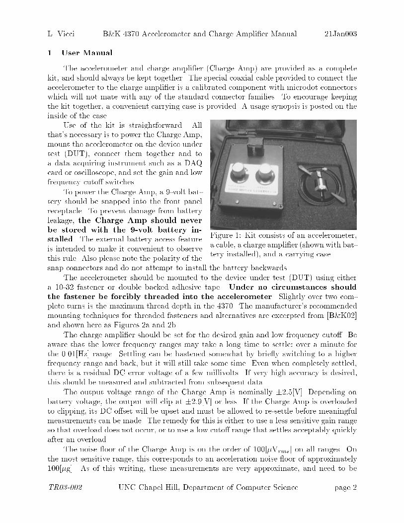
The accelerometer and charge ampli�er �Charge Amp� are provided as a completekit� and should always be kept together The special coaxial cable provided to connect theaccelerometer to the charge ampli�er is a calibrated component with microdot connectorswhich will not mate with any of the standard connector families To encourage keepingthe kit together� a convenient carrying case is provided A usage synopsis is posted on theinside of the case
Figure �� Kit consists of an accelerometer�a cable� a charge ampli�er �shown with bat�tery installed�� and a carrying case
Use of the kit is straightforward Allthat�s necessary is to power the Charge Amp�mount the accelerometer on the device undertest �DUT�� connect them together and toa data acquiring instrument such as a DAQcard or oscilloscope� and set the gain and lowfrequency cuto� switches
To power the Charge Amp� a ��volt bat�tery should be snapped into the front panelreceptacle To prevent damage from batteryleakage� the Charge Amp should never
be stored with the ��volt battery in�
stalled� The external battery access featureis intended to make it convenient to observethis rule Also please note the polarity of thesnap connectors and do not attempt to install the battery backwards
The accelerometer should be mounted to the device under test �DUT� using eithera ����� fastener or double backed adhesive tape Under no circumstances should
the fastener be forcibly threaded into the accelerometer� Slightly over two com�plete turns is the maximum thread depth in the ���� The manufacturer�s recommendedmounting techniques for threaded fasteners and alternatives are excerpted from B�K��and shown here as Figures �a and �b
The charge ampli�er should be set for the desired gain and low frequency cuto� Beaware that the lower frequency ranges may take a long time to settle� over a minute forthe � ��Hz range Settling can be hastened somewhat by brie�y switching to a higherfrequency range and back� but it will still take some time Even when completely settled�there is a residual DC error voltage of a few millivolts If very high accuracy is desired�this should be measured and subtracted from subsequent data
The output voltage range of the Charge Amp is nominally ����V Depending onbattery voltage� the output will clip at ����V or less If the Charge Amp is overloadedto clipping� its DC o�set will be upset and must be allowed to re�settle before meaningfulmeasurements can be made The remedy for this is either to use a less sensitive gain rangeso that overload does not occur� or to use a low cuto� range that settles acceptably quicklyafter an overload
The noise �oor of the Charge Amp is on the order of ����Vrms on all ranges Onthe most sensitive range� this corresponds to an acceleration noise �oor of approximately����g As of this writing� these measurements are very approximate� and need to be
TR������ UNC Chapel Hill� Department of Computer Science page �

L Vicci B�K ���� Accelerometer and Charge Ampli�er Manual ��Jan���
Figure �a� Mounting techniques excerpted from B�K��
quanti�ed more carefully if the kit is to be used at sensitivities where this is an issue The upper cuto� frequency� or �dB rollo� point of the Charge Amp�s passband is
nominally � �kHz In the stopband� a special rejection band is provided to suppress theresonance peak of the accelerometer over the range of �����kHz in which it can occur This provides at least ��dB anti�alias �ltering for all mechanical excitation above ��kHz�
TR������ UNC Chapel Hill� Department of Computer Science page �

L Vicci B�K ���� Accelerometer and Charge Ampli�er Manual ��Jan���
Figure �b� Alternative techniques excerpted from B�K��
irrespective of the accelerometer resonance Refer to page �� of the design drawings fordetailed response curves� as simulated by SPICE
The output of the charge ampli�er will drive any single�ended instrument inputimpedance of � ��� through a conventional BNC cable It should be relatively insensi�tive to ground loops between the accelerometer and the driven instrument However careshould be taken to prevent the Charge Amp box from electrically contacting anything�as ground loops between the accelerometer and the Charge Amp itself can cause noiseproblems The Charge Amp is furnished with rubber feet to help provide the necessaryelectrical isolation
TR������ UNC Chapel Hill� Department of Computer Science page �

L Vicci B�K ���� Accelerometer and Charge Ampli�er Manual ��Jan���
� Charge Amp Theory of Operation
The Charge Amp is logically composed of �ve functional blocks and a power manage�ment block Referring to Figure �� these are the charge integrating preampli�er preamp�two stages of anti�alias �lter cauer� and cauer�� an integrating feedback circuit dcfb� anoutput driver di�out� and power management pwrgnd Also shown is an electrical modeltdcr of the accelerometer in which the acceleration stimulus is represented by voltage Va
TITLE
B&K 4370 Charge amplifierDESCRIPTION
Charge amplifier, 10[mHz] to 10[kHz]with SPICE nodes and subckts shown
DRAWN BY Leandra Vicci
DATE 30 Dec, 2002
MSLSHEET 1 OF 15SCALE 1: 1.5
DWG NO
REV 4.0
SIZE
A
Va
U2U1 U3 U4C0
Vp
Vn pwrgnd
U50
B1
dcfb
R5
R6n
R0m 5out
0
U1b
R1mR2mC2in234
U2a
R3R467
tdcr
Cp
Csain 0
qout
diffout
U2b
R1 R2
R3
R4
in 1
out
2com
0
C2
C4
preamp
U1a
C0n
sum
out
0
in
R1
cauer1
R2
R3R4
R6
R1
U3a
U3b
+
-
-+
C5
C1
1
2
3
4
in
out
0
C4 C3
cauer2
R2
R3R4
R6
R1
U4a
U4b
+
-
-+
C5
C1
1
2
3
4
in
out
0
C4 C3
Notes:1. R6 and C0 are gang switchable for three gain ranges.2. R1, R2, and R0 are gang switchable for four low cutoff points.
Figure �� Charge Amp schematic showing SPICE subcircuits
��� pwrgnd
The Charge Amp uses a single ��volt battery� and needs to have a local ground refer�ence� preferably midway between the positive and negative power rails This is generatedby U�� a TLE���� Virtual Ground Generator This local virtual ground is connected tothe instrument�s case and through the connecting cable to the body of the ���� It istherefore important not to allow a ground loop to be established between the ���� and theCharge Amp The Charge Amp has insulating rubber feet to isolate it from its supportingsurface
TR������ UNC Chapel Hill� Department of Computer Science page �

L Vicci B�K ���� Accelerometer and Charge Ampli�er Manual ��Jan���
��� di�out
Ground loop noise between the Charge Amp and the instrument it drives is howeversuppressed U�b is embedded in a di�erential ampli�er con�guration which isolates thelocal ground from the output common This prevents a ground loop from occurring betweenthe Charge Amp and the driven instrument The amount of ground noise suppressiondepends on the CMRR of the di�erential con�guration of di�out which should approach��dB
��� tdcr
The resonance of the ���� is not explicitly modeled here� but the acceleration stimulus�including gravity� is represented by Va Changes in Va cause a charge transfer through thetranscapacitance element Cs Parallel capacitance Cp comprises the parasitic capacitanceof the ���� and its connecting cable The transcapacitance gain was chosen to match themanufacturer�s sensitivity data so that Va � �V represents an acceleration of �m�s� Note that this is strictly a simulation model
��� preamp
This is the integrating ampli�er which transduces charge to voltage The transelas�tance gain is the reciprocal of capacitance C� The preamp also provides one real poleto the �fth�order anti�alias �lter The frequency of this pole is established by R� and theparallel combination of Cs and Cp Gain ranges are implemented with switch selectablecapacitances of �� ��� and ���nF for C� Operation at very low frequency requires anampli�er with a low noise �oor as well as very low bias current U� is a TLC����C duallow�noise precision op amp implemented in TI�s LinCMOS technology� with �pA typicalbias current and ��nV�
pHz at ��Hz �in the ��f noise regime� TI��a
�� cauer� and cauer�
Each of these circuits provides two complex poles and two complex zeros to the anti�alias �lter These poles along with one real preamp pole implement a �fth order lowpass Butterworth function The four complex zeros provide the desired signal suppressionover the frequency range of �� �kHz through �� �kHz to cancel out the ���� resonance Refer to pages ����� of the design drawings for a quantitative comparison �� �kHz isthe resonance of the ���� mounted on a very large DUT mass� while �� �kHz is theresonance of the unmounted device The circuits themselves are nullor realizations ofgeneralized impedance converter �GIC� derived biquadratic functions Chen��
�� dcfb
This circuit sets the low frequency cuto� of the Charge Amp In combination withthe accelerometer transfer function and the preamp transelastance� it implements a crit�ically damped second order high pass �lter function �that is� second order Butterworth� This function has two DC zeros and a pair of complex conjugate poles which set the cut�o� frequency This provides a ��dB�decade rollo� below the switch selectable cuto�frequencies of ��� �� � �� and � ��Hz �see page �� of the design drawings�
TR������ UNC Chapel Hill� Department of Computer Science page �

L Vicci B�K ���� Accelerometer and Charge Ampli�er Manual ��Jan���
The dcfb circuit itself synthesizes the equivalent of a parallel RL circuit which isconnected across C� in the preamp Accounting for the combined DC gain A of the Cauer�lter sections we have�
R �R�R�R�
AR�R�
� L �R�R�R�C�
AR�
�
The equivalent feedback impedance of the preamp circuit is then�
Z� ��
���ZRL � sC���
�
C�
s
s� � s����Q�� � ��
�
� where
Q� �RpL�C�
�
sR�R�R�C�
AR�
�R�C�
� and
�� ��pLC�
�
rAR�
R�R�R�C�C�
�
The �lter poles come from the denominator of Z�� with the cuto� frequency determinedby �� and the damping factor by Q� These parameters are highly underconstrained inthat the number of determining component values �degrees of freedom� is large Compo�nent values were chosen to implement the desired low cuto� for the various ranges whileproviding the desired Butterworth function for each range
References
B�K�� Product Data � Piezoelectric DeltaShear Accelerometers Uni�Gain� Delta�Tron and Special Types�! http�www�bksv�compdfBp����pdf�Br�uel�Kj�r� October ��� ����
Chen�� Wai�Kan Chen� Ed � The Circuits and Filters Handbook�! CRC Press� �����ISBN �������������� pp ���������
TI��a Texas Instruments Data Book� !Ampli�ers� Comparators� and Special Func�tions�! Texas Instruments� ����� SLYD���A� vol A� pp ������
TI��b Texas Instruments Data Book� !Ampli�ers� Comparators� and Special Func�tions�! Texas Instruments� ����� SLYD���A� vol B� pp ������
APPENDIX A � Design drawings
The following are the design drawings of the as�built Charge Amp
TR������ UNC Chapel Hill� Department of Computer Science page �

TIT
LE
B&
K 4
370
Cha
rge
ampl
ifier
DE
SC
RIP
TIO
N Cha
rge
ampl
ifier
, 10[
mH
z] to
10[
kHz]
with
SP
ICE
nod
es a
nd s
ubck
ts s
how
nD
RA
WN
BY
Lean
dra
Vic
ci
DA
TE
30 D
ec, 2
002
MS
LS
HE
ET
1 O
F 1
5S
CA
LE1:
1.5
DW
G N
O
RE
V4.
0
SIZ
E A
Va
U2
U1
U3
U4
C0
Vp Vn
pwrg
nd
U5
0
B1
dcfb
R5
R6 n
R0 m
5ou
t
0
U1b
R1 m
R2 m
C2
in2
34
U2a
R3
R4
67
tdcr Cp
Cs
ain
0
qout
diff
out
U2b
R1
R2
R3
R4
in1
out
2co
m
0
C2
C4
prea
mp
U1aC0 n
sum
out
0
inR1
caue
r1
R2R
3R
4
R6
R1
U3a
U3b
+ -
- +
C5 C
1
12 3
4
in
out
0
C4
C3
caue
r2
R2R
3R
4
R6
R1
U4a
U4b
+ -
- +
C5 C
1
12 3
4
in
out
0
C4
C3
Not
es:
1. R
6 an
d C
0 ar
e ga
ng
sw
itcha
ble
for
thre
e
gai
n ra
nges
.2.
R1,
R2,
and
R0
are
g
ang
switc
habl
e fo
r
four
low
cut
off p
oint
s.

U2
U1
U3
U4
C50
pwrg
nd
C54
C51
C52
C53
U5
8 4
8 4
8 4
8 4
D51
B1
diff
out
U2b
R41
R42
R43
R44
7
6 5
C42
C44
caue
r1
R22R
23R
24
R26
R21
U3a
U3b
+ -
- +
C25 C
21
C24
7
6 5
1
23
C23
caue
r2
R32R
33R
34
R36
R31
U4a
U4b
+ -
- +
C35 C
31
C34
7
6 5
1
23
C33
prea
mp
U1a
C0c
R1
1
2 3
C0b
C0a
Sw
2a
TIT
LE
B&
K 4
370
Cha
rge
ampl
ifier
DE
SC
RIP
TIO
N Cha
rge
ampl
ifier
, 10[
mH
z] to
10[
kHz]
Sch
emat
ic D
iagr
amD
RA
WN
BY
Lean
dra
Vic
ci
DA
TE
30 D
ec, 2
002
MS
LS
HE
ET
2 O
F 1
5S
CA
LE1:
1.5
DW
G N
O
RE
V4.
0
SIZ
E A
dcfb
R15
R16
a
R10
b
U1b
C12
1
2
U2a
R13
R14
3
7
6 5
R10
a
R10
c
R16
bR
11b
R11
c
R11
a
R12
b
R12
a
R12
cS
w1a
Sw
1bS
w1c Sw
2b
R12
d
R11
dR
10d
Sw
2c

R21
10K
R22
15K
R23
10K
R24
10K
R26
16.
9KR
31 7
.5K
R32
24.
9KR
33 1
0KR
34 1
0KR
36 1
0KR
41 1
0.7K
R42
10K
R43
10.
7KR
44 1
0K
TIT
LE
B&
K 4
370
Cha
rge
ampl
ifier
DE
SC
RIP
TIO
N Cha
rge
ampl
ifier
, 10[
mH
z] to
10[
KH
z]C
ompo
nent
list
DR
AW
N B
YLe
andr
a V
icci
DA
TE
30 D
ec, 2
002
MS
LS
HE
ET
3 O
F 1
5S
CA
LE1:
1.5
DW
G N
O
RE
V4.
0
SIZ
E A
ICs
& D
iod
esD
51 1
N41
48U
1 T
LC22
02C
U2
TLE
2142
CU
3 T
LE21
42C
U4
TLE
2142
CU
5 T
LE24
26
Cap
acit
ors
C0a
1.0
nFC
0b 1
0nF
C0c
100
nFC
12 5mF
C23
10p
FC
24 1
0pF
C21
999
.1pF
C25
987
.4pF
C33
10p
FC
34 1
0pF
C31
3.3
25nF
C35
330
.3pF
C42
220
pFC
44 2
20pF
C50
100
uFC
51 0
.1mF
C52
0.1mF
C53
0.1mF
C54
0.1mF
Res
isto
rsR
1 1
3.3K
R10
a 1
GR
10b
100
MR
10c
10M
R10
d 1
MR
11a
6.2
MR
11b
620
KR
11c
62K
R11
d 6
.2K
R12
a 6
.2M
R12
b 6
20K
R12
c 6
2KR
12d
6.2
KR
13 1
00K
R14
100
KR
15 1
00K
R16
a 1
KR
16b
10K

TIT
LE
B&
K 4
370
Cha
rge
ampl
ifier
DE
SC
RIP
TIO
N Cha
rge
ampl
ifier
, 10[
mH
z] to
10[
kHz]
Boa
rd la
yout
DR
AW
N B
YLe
andr
a V
icci
DA
TE
30 D
ec, 2
002
MS
LS
HE
ET
4 O
F 1
5S
CA
LE1.
8: 1
DW
G N
O
RE
V4.
0
SIZ
E A
C33
C54
U4
C31
R32R31
R33R
36
R34
C34
C35
C23
C53
U3
C21
R22R21
R23R
26
R24
C24
C25
U2
U1
C12
R43R44R41R42
R13R14
R15
R10b
-
+C
50
U5
D51
C51
C52
R10a
R12
aR
12b
R12
c
R11
aR
11b
R11
c
R16
aR
16b
C0a
C0b
C0c
R1
R10c
B+
R12
d
R11
d
R10d
B-
1
2 4 536 8 97
10
1112
1314
15 16
17
1819
202122ou
tco
m
in
gnd
C44
C42

TIT
LE
B&
K 4
370
Cha
rge
ampl
ifier
DE
SC
RIP
TIO
N Cha
rge
ampl
ifier
, 10[
mH
z] to
10[
kHz]
Mec
hani
cal r
elat
ions
hips
DR
AW
N B
YLe
andr
a V
icci
DA
TE
30 D
ec, 2
002
MS
LS
HE
ET
5 O
F 1
5S
CA
LE1:
1
DW
G N
O
RE
V4.
0
SIZ
E A
-
+
C12
C12
C12

TIT
LE
B&
K 4
370
Cha
rge
ampl
ifier
DE
SC
RIP
TIO
N Cha
rge
ampl
ifier
, 10[
mH
z] to
10[
kHz]
Box
mec
hani
cals
DR
AW
N B
YLe
andr
a V
icci
DA
TE
30 D
ec, 2
002
MS
LS
HE
ET
6 O
F 1
5S
CA
LE1:
1.2
DW
G N
O
RE
V4.
0
SIZ
E A
Not
es:
1. In
dex
from
face
s at
the
botto
m o
f the
box
.2.
Inde
x fr
om fa
ce a
t the
top
of th
e bo
x.3.
Box
: Ham
mon
d M
fg. 1
590C
BK
1.53
3
0.35
8
1.10
8
4.23
3
0.52
51.15
0
2.40
03.02
5
1.12
5
0.75
3
2.95
3
1.00
0
Not
e 1
Not
e 2
TIT
LE
B&
K 4
370
Cha
rge
ampl
ifier
DE
SC
RIP
TIO
N Cha
rge
ampl
ifier
, 10[
mH
z] to
10[
kHz]
Box
lid
mec
hani
cals
DR
AW
N B
YLe
andr
a V
icci
DA
TE
30 D
ec, 2
002
MS
LS
HE
ET
7 O
F 1
5S
CA
LE1:
1.2
DW
G N
O
RE
V4.
0
SIZ
E A
0.56
7
1.06
7
2.71
52.
980
1.10
3
1.41
5
2.29
0
2.60
3
1.36
8
2.86
8
1/8"
dril
l,2
plac
es
3/8"
dril
l,2
plac
es
cut w
ith3/
16"
end
mill
4.37
5
1.20
2
3.20
2
#30
drill
,2
plac
es

#36
drill
, the
n ta
p6-
32 N
C, 4
pla
ces
#41
drill
,2
plac
es
3/8
end
mill
,2
plac
es
cut w
ith3/
16"
end
mill
1.50
0
0.12
50.
313 0.
525 0.
7501.
025 1.18
8 1.37
5
0.12
5
0.25
0
0.50
0
0.75
0
0.87
5
1.00
0
TIT
LE
B&
K 4
370
Cha
rge
ampl
ifier
DE
SC
RIP
TIO
N Cha
rge
ampl
ifier
, 10[
mH
z] to
10[
kHz]
Bat
tery
hol
der m
echa
nica
lsD
RA
WN
BY
Lean
dra
Vic
ci
DA
TE
30 D
ec, 2
002
MS
LS
HE
ET
8 O
F 1
5S
CA
LE2:
1
DW
G N
O
RE
V4.
0
SIZ
E A
0.75
0
0.50
00.
625
Mat
eria
l: R
igid
, non
-brit
tle,
mac
hina
ble
insu
lato
r su
ch a
s ny
lon
or p
olyp
ropy
lene
.
#36
drill
2.00
0

0.01
0.1
1.0
1010
010
1O
FF
LO
W C
UT
OF
F [
Hz]
RA
NG
E [
mV
/m/s
2 ]
CH
AR
GE
AM
PL
IFIE
R F
OR
B&
K43
70
TIT
LE
B&
K 4
370
Cha
rge
ampl
ifier
DE
SC
RIP
TIO
N Cha
rge
ampl
ifier
, 10[
mH
z] to
10[
kHz]
Fro
nt p
anel
labe
lD
RA
WN
BY
Lean
dra
Vic
ci
DA
TE
30 D
ec, 2
002
MS
LS
HE
ET
9 O
F 1
5S
CA
LE1:
1
DW
G N
O
RE
V4.
0
SIZ
E A

TIT
LE
B&
K 4
370
Cha
rge
ampl
ifier
DE
SC
RIP
TIO
N Cha
rge
ampl
ifier
, 10[
mH
z] to
10[
kHz]
Car
ryin
g ca
se a
nd w
arni
ng l
abel
sD
RA
WN
BY
Lean
dra
Vic
ci
DA
TE
30 D
ec, 2
002
MS
LS
HE
ET
10 O
F 1
5S
CA
LE1:
1
DW
G N
O
RE
V4.
0
SIZ
E A
B&
K43
70 A
CC
EL
ER
OM
ET
ER
AN
D C
HA
RG
E A
MP
LIF
IER
KIT
Mic
roel
ectr
on
ic S
yste
ms
Lab
ora
tory
, Dep
artm
ent
of
Co
mp
ute
r S
cien
ce, U
NC
CH
INS
TR
UC
TIO
N S
UM
MA
RY
• In
stal
l 9-v
olt
bat
tery
.•
Mo
un
t ac
cele
rom
eter
an
dco
nn
ect
to c
har
ge
amp
lifie
r.•
Co
nn
ect
BN
C c
on
nec
tor
to a
sco
pe
or
oth
er in
stru
men
t.•
Up
per
cu
toff
fre
qu
ency
is6.
8[kH
z]. P
LE
AS
E D
O•
Sto
re a
ll p
arts
of
kit
tog
eth
er.
DO
NO
T•
Sto
re w
ith
bat
tery
inst
alle
d.
• In
sert
fas
ten
er m
ore
th
an 2
turn
s in
to a
ccel
ero
met
er.
Larg
est d
iago
nal 1
.175
Larg
est h
t 0.6
68la
rges
t wd
1.03
8
+
-0.
668
(0.6
5)
1.03
8 (1
.025
)
1.81
3 (1
.70)
0.12
5
TIT
LE
B&
K 4
370
Cha
rge
ampl
ifier
DE
SC
RIP
TIO
N Cha
rge
ampl
ifier
, 10[
mH
z] to
10[
kHz]
9-vo
lt ba
ttery
DR
AW
N B
YLe
andr
a V
icci
DA
TE
31 D
ec, 2
002
MS
LS
HE
ET
11 O
F 1
5S
CA
LE2:
1
DW
G N
O
RE
V4.
0
SIZ
E A

TIT
LE
B&
K 4
370
Cha
rge
ampl
ifier
DE
SC
RIP
TIO
N Cha
rge
ampl
ifier
, 10[
mH
z] to
10[
kHz]
Circ
uit p
hoto
s, to
p an
d bo
ttom
DR
AW
N B
YLe
andr
a V
icci
DA
TE
16 J
an, 2
003
MS
LS
HE
ET
12 O
F 1
5S
CA
LE1:
1
DW
G N
O
RE
V4.
0
SIZ
E A
No
te: C
42 a
nd C
44 w
ere
adde
daf
ter
thes
e ph
otos
wer
e ta
ken.

-180
-160
-140
-120
-100-80
-60
-40
-200
1[m
Hz]
10[m
Hz]
100
[mH
z]1
[Hz]
10 [Hz]
100
[Hz]
1[k
Hz]
10[k
Hz]
100
[kH
z]1
[MH
z]F
requ
ency
SP
ICE
sim
ulat
ion
of C
harg
e A
mpl
ifier
res
pons
e cu
rves
for
G1k
= 1
00 [m
V/m
/s2 ]
Gain [db(V/m/s2)]
flo = 10 [Hz]
flo = 1 [H
z]
flo = 100 [mHz]
flo = 10 [mHz]
TIT
LE
B&
K 4
370
Cha
rge
ampl
ifier
DE
SC
RIP
TIO
N Cha
rge
ampl
ifier
, 10[
mH
z] to
10[
kHz]
SP
ICE
sim
ulat
ions
of a
s de
sign
ed c
ircui
tD
RA
WN
BY
Lean
dra
Vic
ci
DA
TE
17 J
an, 2
003
MS
LS
HE
ET
13 O
F 1
5S
CA
LE1:
1
DW
G N
O
RE
V4.
0
SIZ
E A

G1k
= 1
00 [m
V/m
/s^2
]
-100-9
0
-80
-70
-60
-50
-40
-30
-20
-10
Fre
quen
cy
-140
-130
-120
-110
1m
Hz
10 mH
z10
0m
Hz
1 Hz
10 Hz
100
Hz
1kH
z10 kH
z10
0kH
z1
MH
z
G1k
= 1
0 [m
V/m
/s^2
]
G1k
= 1
[mV
/m/s
^2]
Gain [db(V/m/s2)]S
PIC
E s
imul
atio
n of
Cha
rge
Am
plifi
er r
espo
nse
curv
es fo
r F
lo =
10
[mH
z]
TIT
LE
B&
K 4
370
Cha
rge
ampl
ifier
DE
SC
RIP
TIO
N Cha
rge
ampl
ifier
, 10[
mH
z] to
10[
kHz]
SP
ICE
sim
ulat
ions
of a
s de
sign
ed c
ircui
tD
RA
WN
BY
Lean
dra
Vic
ci
DA
TE
17 J
an, 2
003
MS
LS
HE
ET
14 O
F 1
5S
CA
LE1:
1
DW
G N
O
RE
V4.
0
SIZ
E A

+ 40
dB
+ 30
+ 20
+10
0
-10
Calibration Chart for Accelerom..., Type 4370
j Serial no .... BZ.l R .Q.Q ....... . --A......_ '-ltMty at ...... S.Q .... Hut ... .:1.~ ...... °C
Cllllle c.ecltance ~f .....•.... ..1./.0 ....................... pF
c ..... leneivitv••
......... }t,/Ua .... pC/ms-2.or ........... <-t.l,k .... pC/g"
V .... leMitivity••
............ ~.2. ... mV/ms-2,or .......... R.f,.fi ..... mV/g
~ .... _(including cablel ............. U.'-8. . ...... pF
Maximum Tranaveraa Sanaitivity at 30Hz ... .'!I,D ... %
Weltht ............... 5.'-f,.O ....... grams
Unc~Mnped natural frequency ........... 2.1, ........... kHz For mountacl Reaonant Frequency and for Frequency Reapoi'IH relative to Reference Sensitivity .... attachacl individual Frequency R81P0fl88 Curve
Polerity is poeitive =center of the c:qn_nector for an acceleration dir from lhe mounting surface into the body of the terom«er.
Realatence minimum 20000Mn~ room temperature.
Date .2:-.J.a.~.-u ... Signa._. ......... ::r;; ................ . • 1 g • 8,B07 ms-'-2
•• This calibration is traceable to the National Bureau of Standards Washington D.C.
IIC 01!10
pate: Potentiometer:
)0 500 1 kHz 2 5
Typical Temperatura Seneltivity Error in dB rei. the Reference Values Individual deviation max. ± 1 dB
-d•'o1----s~o--~1+oo~~150~---2oo~--~250~--~3oo~•c 32 122 212 302 312 482 572°F
Phy8ical: 79o39l
!:~ Material: Stainless Steel W-, IIi'
I Mounting Thread: 10-32 UNF-2B
Electrical Connector: Coaxial 10-32 UNF-2A thread
Environmental: Humidity: Seaied Max. Temperature: 250"C or 4B2°F Max. Continuous Sinuaoidal Ace. (peakl:
20000ms-2or 2000g Max. Shock Acceleration: 50000 ms-2 or 5000 g Typical Magnetic Sensitivity (50 Hzl: f.2 m$-2/T or
0,012 g/kgauss Typical Temperature Transient Sensitivity:
(Low. Lim. Freq.: 3 Hzl O.OB ms-2;oc or O.OOB g/°C Typical Baee Strain Sensitivity:
0.003 ms-2/pstrafn or 0,0003 g/pstrain
For further information see B & K "Piezoelectric Accelerometer and Preamplifier" Handbook.
Zero Level: D A 8 C Lin.
I
\
10 20 '- 50 100 n. Fr~.: ____ Hz Writing. Speed: ____ mm/~c. Paper Speed: ____ mm/sec.
{
·--
j I
:
-
-