benha university faculty of engineering at shoubra l shoubra/electrical... · collector current (i...
TRANSCRIPT
Lecture #3 ( 2 weeks)
Transistors
Instructor: Dr. Ahmad El-Banna
Benha University Faculty of Engineering at Shoubra
Spr
in
g 2
015
ECE-291 Electronic Engineering
© A
hmad
El-B
anna
1
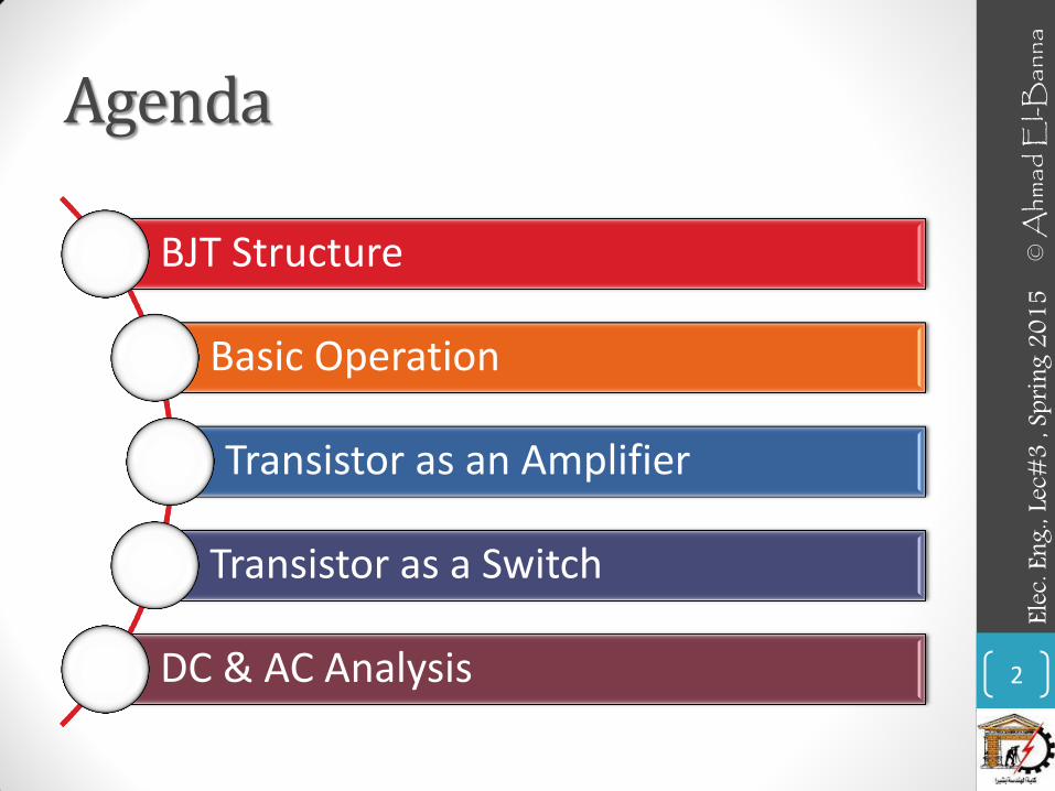
Agenda
BJT Structure
Basic Operation
Transistor as an Amplifier
Transistor as a Switch
DC & AC Analysis 2
Elec.
Eng.,
Lec#
3 , S
prin
g 201
5 ©
Ahm
ad E
l-Ban
na
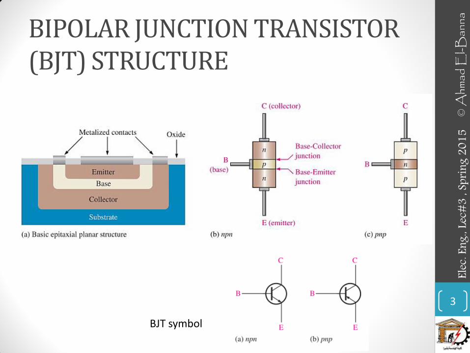
BIPOLAR JUNCTION TRANSISTOR (BJT) STRUCTURE
BJT symbol
3
© A
hmad
El-B
anna
Ele
c. En
g., Le
c#3
, Spr
ing 2
015
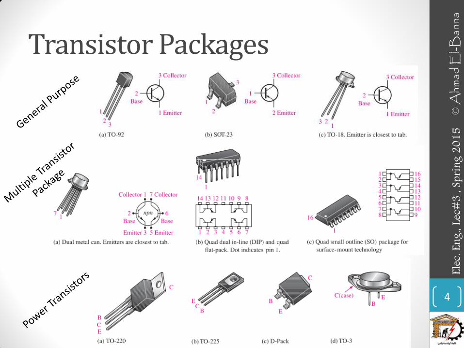
Transistor Packages
4
© A
hmad
El-B
anna
Ele
c. En
g., Le
c#3
, Spr
ing 2
015
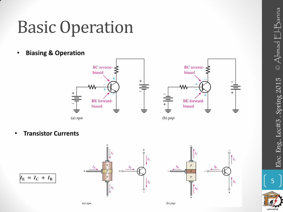
Basic Operation • Biasing & Operation
• Transistor Currents
5
© A
hmad
El-B
anna
Ele
c. En
g., Le
c#3
, Spr
ing 2
015
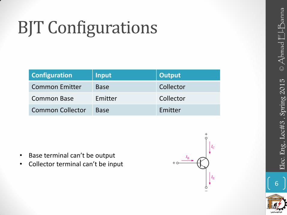
BJT Configurations
Configuration Input Output
Common Emitter Base Collector
Common Base Emitter Collector
Common Collector Base Emitter
• Base terminal can’t be output • Collector terminal can’t be input
6
© A
hmad
El-B
anna
Ele
c. En
g., Le
c#3
, Spr
ing 2
015
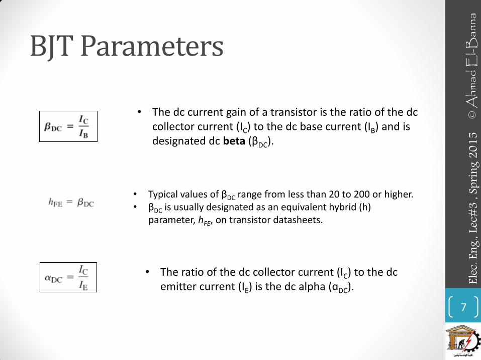
BJT Parameters
• The dc current gain of a transistor is the ratio of the dc collector current (IC) to the dc base current (IB) and is designated dc beta (βDC).
• Typical values of βDC range from less than 20 to 200 or higher. • βDC is usually designated as an equivalent hybrid (h)
parameter, hFE, on transistor datasheets.
• The ratio of the dc collector current (IC) to the dc emitter current (IE) is the dc alpha (ɑDC).
7
© A
hmad
El-B
anna
Ele
c. En
g., Le
c#3
, Spr
ing 2
015
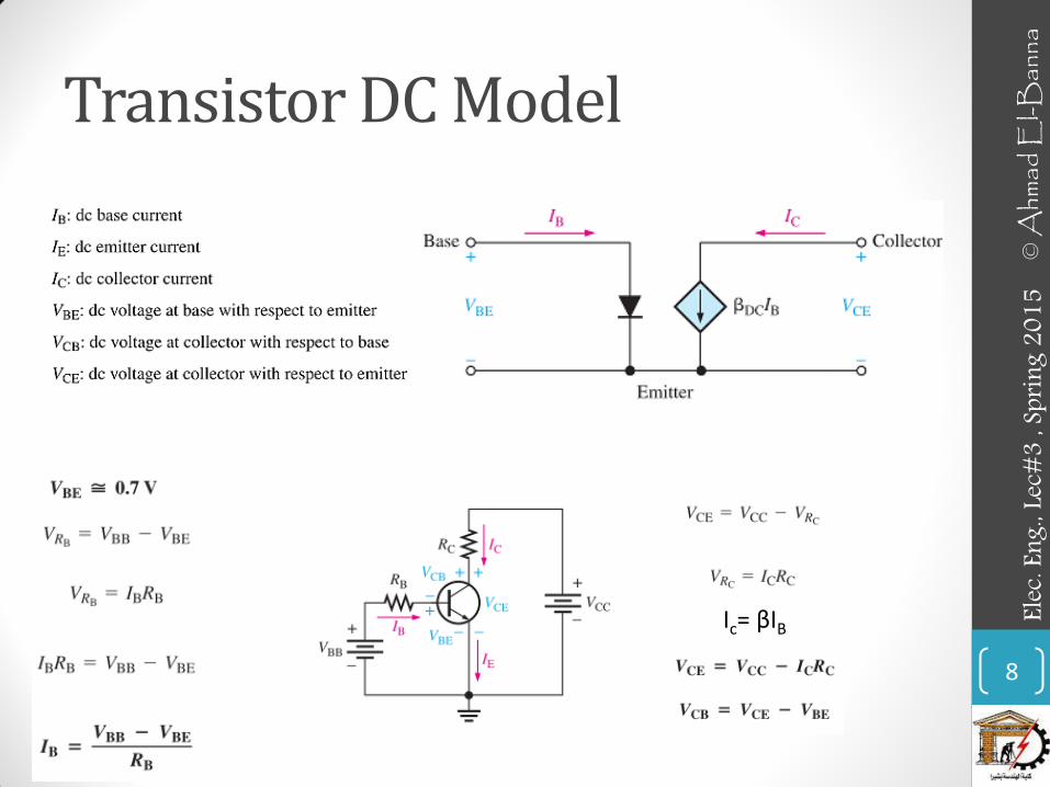
Transistor DC Model
8
© A
hmad
El-B
anna
Ele
c. En
g., Le
c#3
, Spr
ing 2
015
Ic= βIB
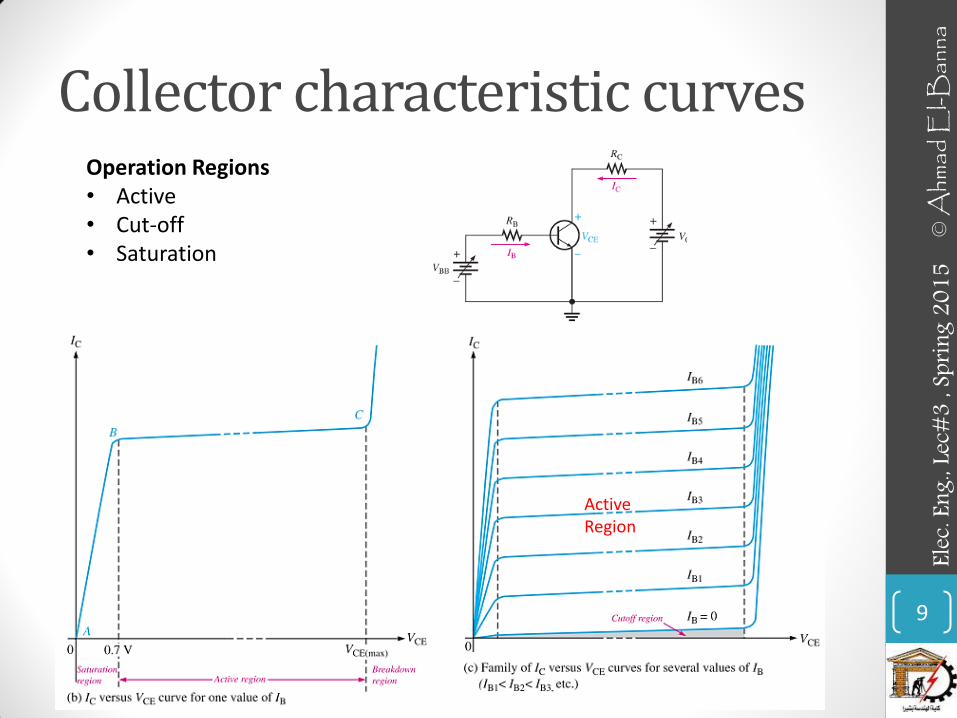
Collector characteristic curves Operation Regions • Active • Cut-off • Saturation
9
© A
hmad
El-B
anna
Ele
c. En
g., Le
c#3
, Spr
ing 2
015
Active Region
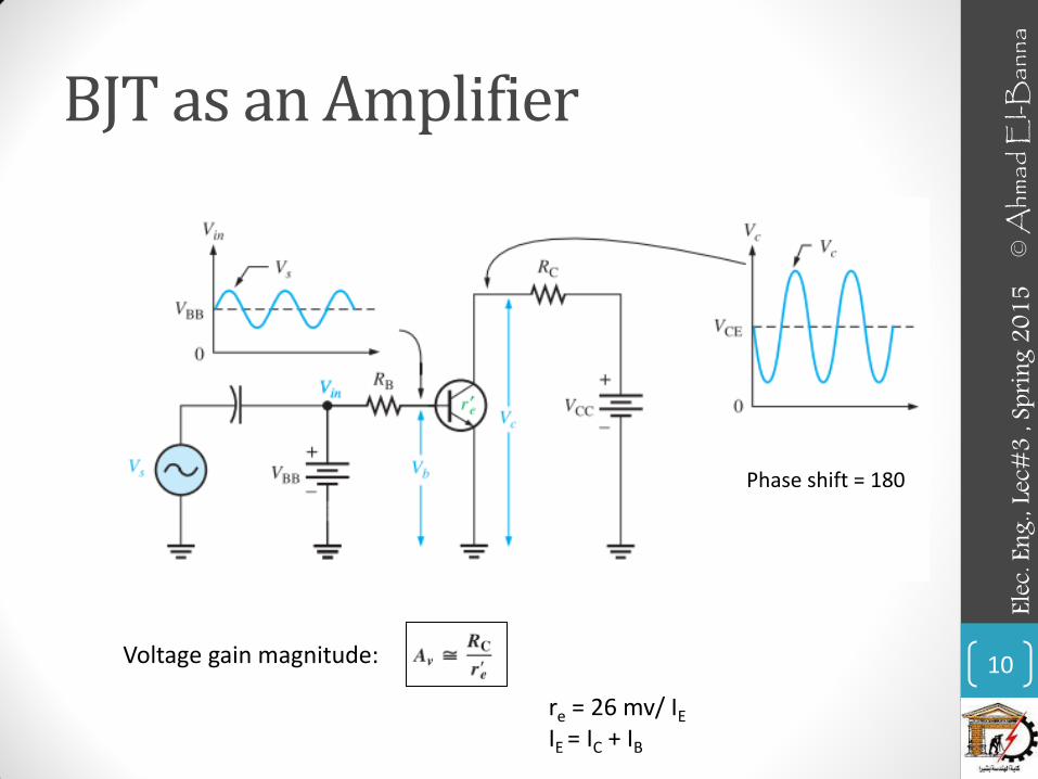
BJT as an Amplifier
10
© A
hmad
El-B
anna
Ele
c. En
g., Le
c#3
, Spr
ing 2
015
Phase shift = 180
re = 26 mv/ IE
IE = IC + IB
Voltage gain magnitude:
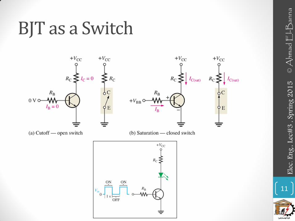
BJT as a Switch
11
© A
hmad
El-B
anna
Ele
c. En
g., Le
c#3
, Spr
ing 2
015
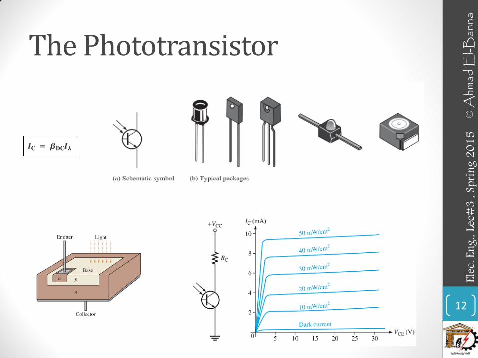
The Phototransistor
12
© A
hmad
El-B
anna
Ele
c. En
g., Le
c#3
, Spr
ing 2
015
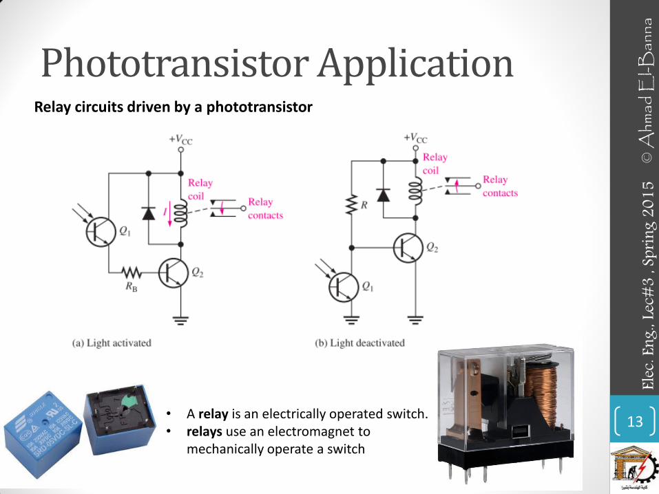
Phototransistor Application Relay circuits driven by a phototransistor
• A relay is an electrically operated switch. • relays use an electromagnet to
mechanically operate a switch
13
© A
hmad
El-B
anna
Ele
c. En
g., Le
c#3
, Spr
ing 2
015
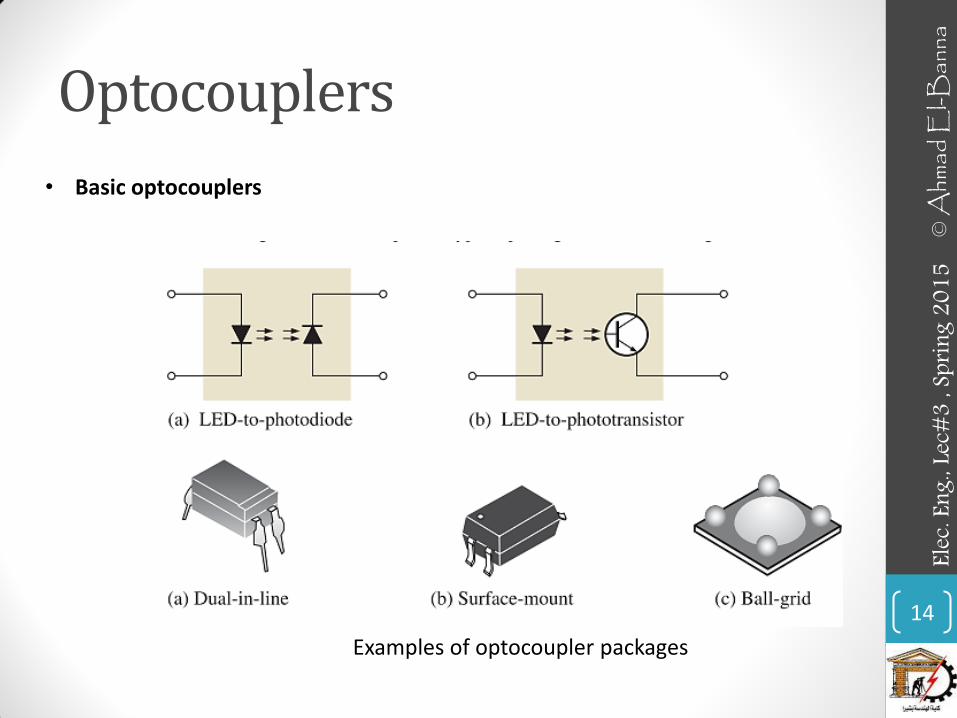
Optocouplers
• Basic optocouplers
Examples of optocoupler packages
14
© A
hmad
El-B
anna
Ele
c. En
g., Le
c#3
, Spr
ing 2
015
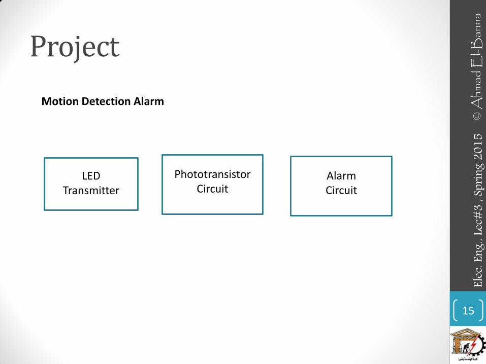
Project
LED Transmitter
Phototransistor Circuit
Motion Detection Alarm
Alarm Circuit
15
© A
hmad
El-B
anna
Ele
c. En
g., Le
c#3
, Spr
ing 2
015

555 Timer Siren Circuit
16
© A
hmad
El-B
anna
Ele
c. En
g., Le
c#3
, Spr
ing 2
015
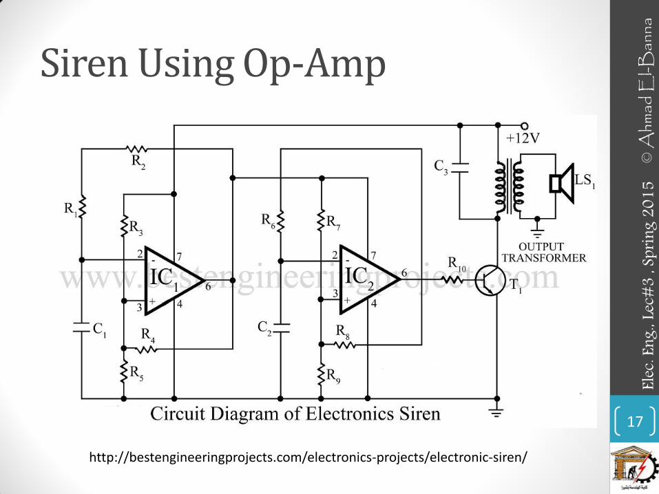
Siren Using Op-Amp
http://bestengineeringprojects.com/electronics-projects/electronic-siren/
17
© A
hmad
El-B
anna
Ele
c. En
g., Le
c#3
, Spr
ing 2
015
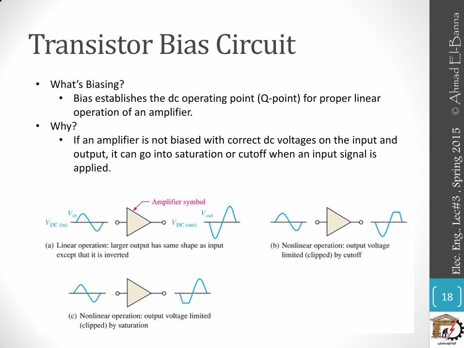
Transistor Bias Circuit • What’s Biasing?
• Bias establishes the dc operating point (Q-point) for proper linear operation of an amplifier.
• Why? • If an amplifier is not biased with correct dc voltages on the input and
output, it can go into saturation or cutoff when an input signal is applied.
18
© A
hmad
El-B
anna
Ele
c. En
g., Le
c#3
, Spr
ing 2
015
19
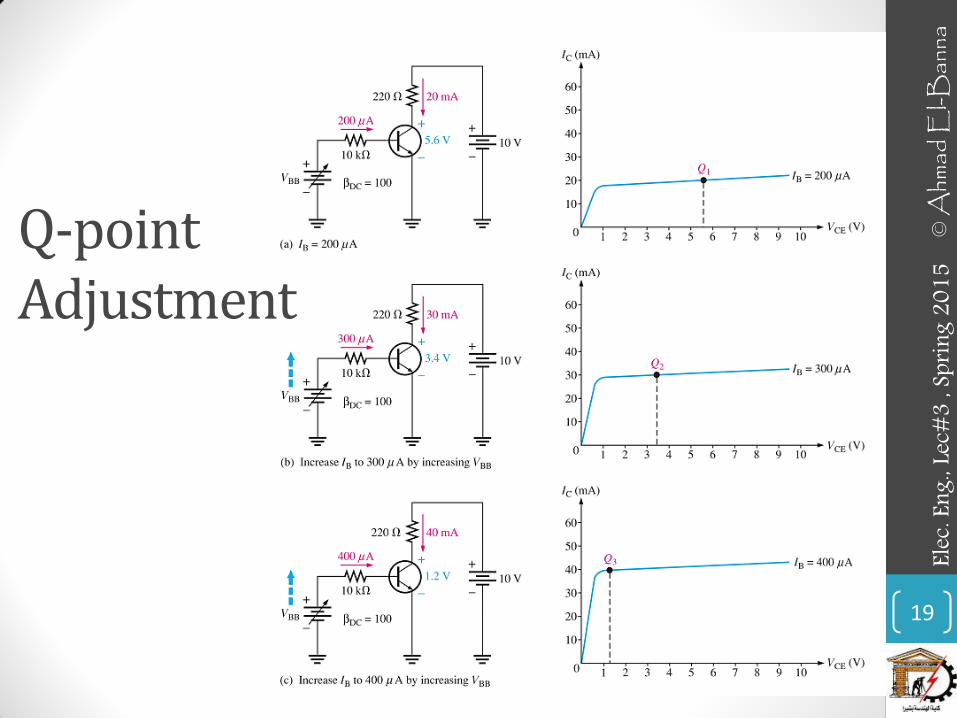
Q-point Adjustment
© A
hmad
El-B
anna
Ele
c. En
g., Le
c#3
, Spr
ing 2
015
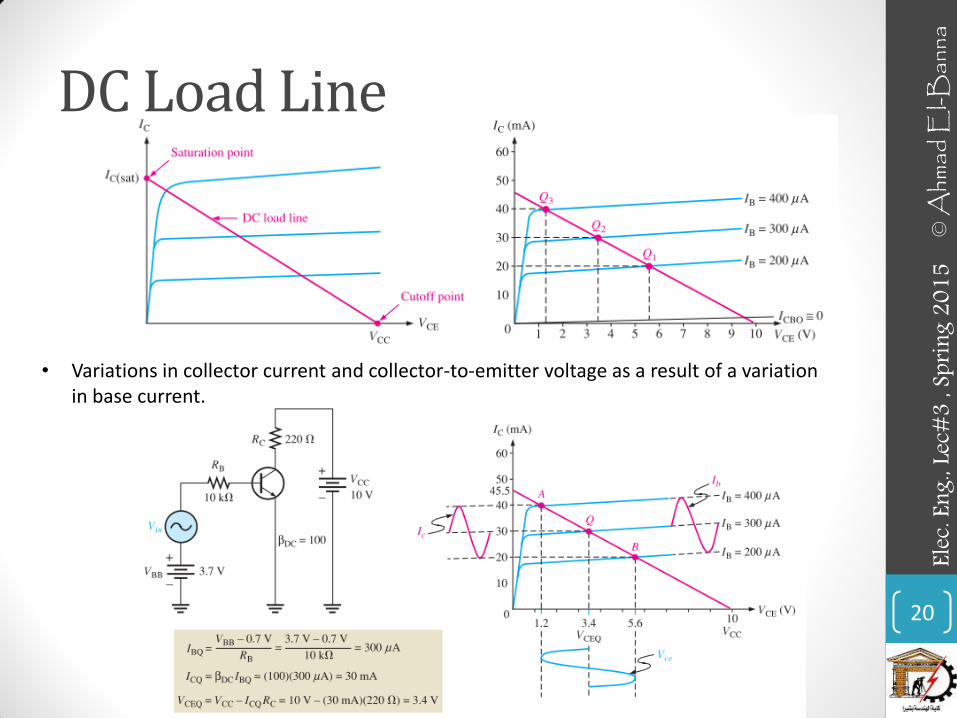
DC Load Line
• Variations in collector current and collector-to-emitter voltage as a result of a variation in base current.
20
© A
hmad
El-B
anna
Ele
c. En
g., Le
c#3
, Spr
ing 2
015
21
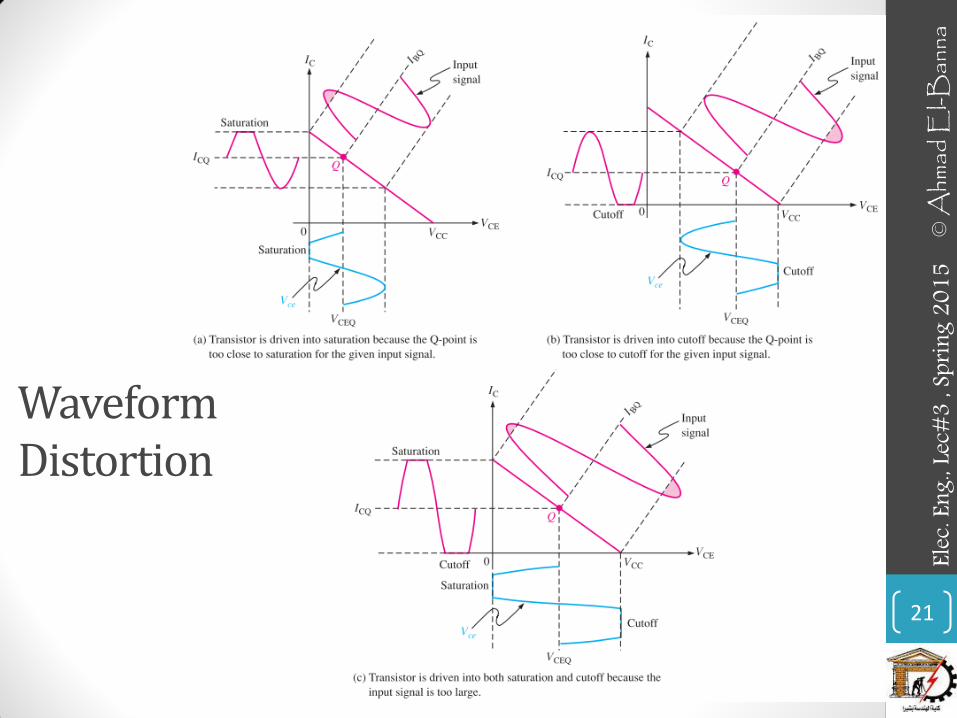
Waveform Distortion
© A
hmad
El-B
anna
Ele
c. En
g., Le
c#3
, Spr
ing 2
015
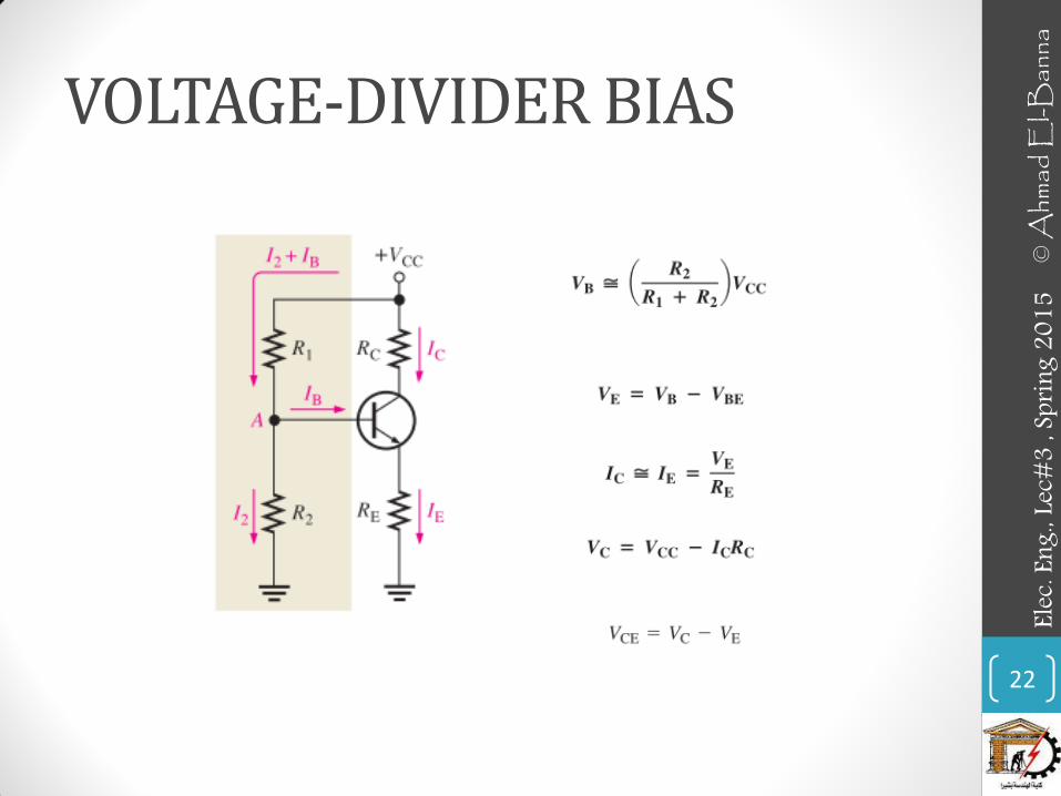
VOLTAGE-DIVIDER BIAS
22
© A
hmad
El-B
anna
Ele
c. En
g., Le
c#3
, Spr
ing 2
015
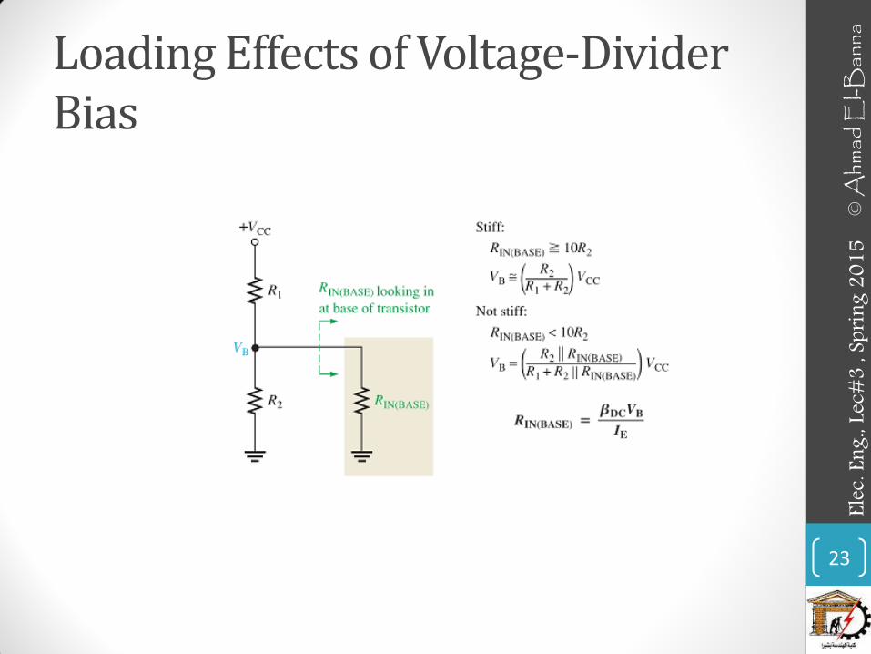
Loading Effects of Voltage-Divider Bias
23
© A
hmad
El-B
anna
Ele
c. En
g., Le
c#3
, Spr
ing 2
015
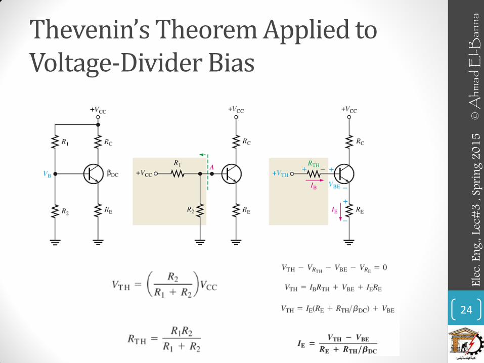
Thevenin’s Theorem Applied to Voltage-Divider Bias
24
© A
hmad
El-B
anna
Ele
c. En
g., Le
c#3
, Spr
ing 2
015
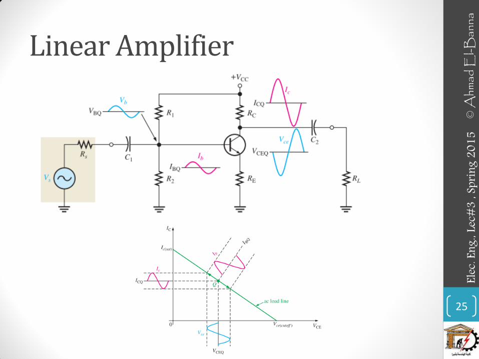
Linear Amplifier
25
© A
hmad
El-B
anna
Ele
c. En
g., Le
c#3
, Spr
ing 2
015
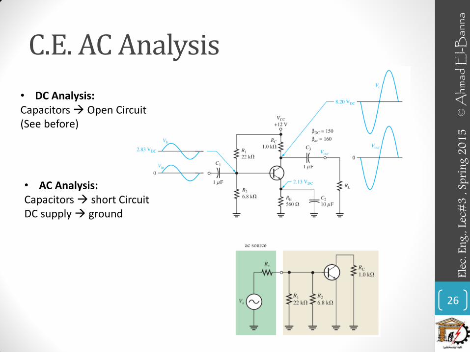
C.E. AC Analysis
• DC Analysis: Capacitors Open Circuit (See before)
• AC Analysis: Capacitors short Circuit DC supply ground
26
© A
hmad
El-B
anna
Ele
c. En
g., Le
c#3
, Spr
ing 2
015
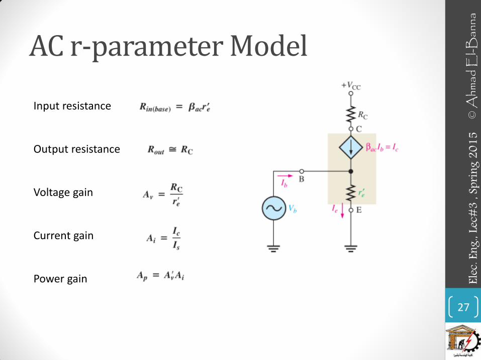
AC r-parameter Model
Input resistance Output resistance Voltage gain Current gain Power gain
27
© A
hmad
El-B
anna
Ele
c. En
g., Le
c#3
, Spr
ing 2
015
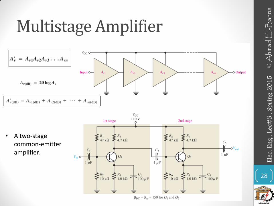
Multistage Amplifier
• A two-stage common-emitter amplifier.
28
© A
hmad
El-B
anna
Ele
c. En
g., Le
c#3
, Spr
ing 2
015
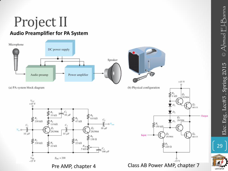
Project II Audio Preamplifier for PA System
Pre AMP, chapter 4 Class AB Power AMP, chapter 7
29
© A
hmad
El-B
anna
Ele
c. En
g., Le
c#3
, Spr
ing 2
015
• For more details, refer to:
• Chapters 4-6, T. Floyd, Electronic Devices and Circuit Theory, 11th edition, Prentice Hall.
• The lecture is available online at: • http://bu.edu.eg/staff/ahmad.elbanna-courses/12136
• For inquires, send to:
30
© A
hmad
El-B
anna
Ele
c. En
g., Le
c#3
, Spr
ing 2
015