benchmarking of tfet analogue circuits: sensors ... · benchmarking of tfet analogue circuits:...
TRANSCRIPT

1
Benchmarking of TFET Analogue
Circuits: Sensors applications
perspective CCS: Dr. M Foysol Chowdhury & Prof. Florin Udrea;
EPFL: Prof A Ionescu & A Biswas Cambridge CMOS Sensors
United Kingdom

Contents • About Cambridge CMOS Sensor. • Low voltage, low power motivation for future sensors. • Benchmark fabricated complementary TFET technology against CMOS.
• Considerations for target high temperature automotive applications.
• Summary
2

About Cambridge CMOS Sensors
• CCS is an ISO9001 certified fabless semiconductor
company with an established high-volume supply
chain. A spin-off company from Cambridge University,
founded in 2008.
• Core products are gas sensors & sensor components
for Consumer and Industrial applications
• Strong patent portfolio in core technology - MEMS
CMOS Micro-hotplates for high volume applications
• Benefits of our technology
• Ultra-low power
• Miniature – smallest gas sensors on the market
• Highly scalable and cost effective CMOS technology
• Ultra-fast thermal transient response
• Highly stable & reliable
2014 Innovation Award Winner
Technology Showcase
Winner
3

Gas Sensor Solutions
• Indoor Air Quality (IAQ) sensor
detects a wide range of indoor air
pollutants
• Alcohol detection for breathalyser
applications
• Carbon Monoxide Toxic Gas
Detection
• World’s Smallest, Lowest Power
multi-gas sensors
• Advanced algorithms for accuracy
& repeatability
Indoor Air Quality monitoring and Breath Analysis in
portable smart devices
4

CCS801 IAQ Sensor
Car
Home
Monitor your
environment
everywhere …
Office
5

Motivations and technological challenges for sensors
Ref: Trillion Sensors Summit – Dr. Jenusz Bryzek
Challenges:
• Ultra-low power
• Miniature
• High reproducibility
• High volume
• Scalable
• Compatible with beyond CMOS
• Reliable
• Low cost
6

All sensors need a common interface to enable future IoT
7
Confidential
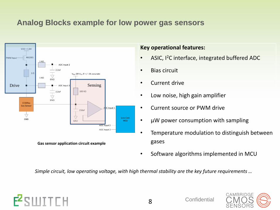
Gas sensor application circuit example
Key operational features:
• ASIC, I2C interface, integrated buffered ADC
• Bias circuit
• Current drive
• Low noise, high gain amplifier
• Current source or PWM drive
• µW power consumption with sampling
• Temperature modulation to distinguish between
gases
• Software algorithms implemented in MCU
Simple circuit, low operating voltage, with high thermal stability are the key future requirements …
Analog Blocks example for low power gas sensors
Drive Sensing
8

Low voltage CMOS Analogue Circuit concepts
One option that is commonly used to achieve low voltage operation is to use the transistor body as a signal input terminal in bulk CMOS. Limitation of body driven circuits in bulk CMOS is that complementary devices are not available since the base substrate is a shared body terminal. On the other hand PDSOI, which provides an isolated body contact for every device, enables complementary body driven circuits and is thus an ideal vehicle for implementing high performance, ultra-low voltage analogue circuits
As a part of our work on the project we investigate and benchmark with a carefully chosen CMOS process node with TFET
9

We considered this process as a node to benchmark for the following reasons: (1) Device is based on same FDSOI wafer
that will typically be used for TFET; (2) Better short-channel effect; (3) Extended body biasing, offers high
performance, low power solutions; (4) Latch up immunity; (5) No channel doping for improved
variability; (6) Ease of porting design from bulk; (7) It has been shown to offer some
performance advantages over finFET or Bulk (e.g. more efficient body biasing (Speed/Power); Extended body bias (speed/leakage) optimization…);
(8) Offers conventional (RVT)* and flipped well (LVT)*.
(a)
(b)
CMOS process node for low voltage circuit STMicroelectronics 28nm, Ultra Thin Body &
Box Fully Depleted Silicon On Insulation (UTBB FD-SOI) process
10
* Regular Voltage Threshold (RVT) and Low Voltage Threshold (LVT)

TFET vs. CMOS current mirror: IOUT /IIN for temperature 25°C to125°C in (left) logarithmic and (right) linear scale.
Typical current mirror IOUT-IIN plots are shown in both logarithmic and linear scale. Simulated results show that TFET current mirror exhibits better thermal stability and linearity as compared to CMOS
Current mirror circuit
11
Simulated benchmarking of 28nm TFET and CMOS Circuit blocks
Iout/Iin = (W2/L2)/(W1/L1)

A differential pair is simulated to show the output current vs VIN and VOUT vs VIN plots. The temperature stability of TFETs are evident even though the gain is lower than CMOS, as expected.
A diode-connected transistor shows TFET has good thermal linearity compared to CMOS
12
Simulated benchmarking of 28nm TFET and CMOS Circuit blocks

TFET
Also Vt shift is used to measure concentration level
With MOSFET and TFET combined with sensor arrays, ultimate goal is it achieve RT ultra-low power AQM sensors
Deblina Sarkar, et al, Tunnel-field-effect-transistor based gas-sensor: Introducing gas detection with a quantum-mechanical transducer, APPLIED PHYSICS LETTERS 102, 023110 (2013)
Claimed TFET can achieve 10000 x sensitivity compared to MOSFET!
TFET as gas sensor for the future?

Other practical considerations
• Market-oriented requirements?
• High temperature automotive?
• ESD
• EM
• Certification
• High current drive
• Etc.
14

Market-oriented parameters
15

Benchmarking Considerations for
Automotive
Electrical hazards in the automotive environment • Source of hazards • Conducted hazards • Radiated hazards • Propagation of electrical hazards • Propagation on the data lines • Hazards on the supply rail • Standards for the protection of automotive electronics
In addition to high temperature and harsh environment
considerations one would need to look at (perhaps beyond the
scopes of this project):
http://www.st.com/st-web-ui/static/active/en/resource/technical/document/application_note/CD00181783.pdf
16

Fig 5.3.7: MHP thermal characteristic.
• Sensor need to operate < 0.5V supply.
• New low voltage CMOS micro-hotplate (MHP) can be designed for < 0.5V operation with maximum operating temperature to 250°C.
• Thermal characteristic of a standard MHP (black line)
• Low voltage MHP characteristic shown in red dotted line.
• What is the maximum drive current TFET device can supply to achieve a target operating temperature?
Design of Low Voltage Micro-Hotplate
17
Benchmarking of 28nm sSi TFETs versus 28nm FD-SOI, CMOS based on a universal compact model for analog circuits shows that: Simulated results of TFET current mirror and differential pair shows better thermal stability and linearity as compared to CMOS. However, the gain TFET differential pair is lower than CMOS, as expected. For the first time using TFET device, we simulated transistor-connected diode using nTFET and pTFET devices where we have shown very high linearity from 0 to 200°C when compared with CMOS. Simulated results also show that when compared to TFET, dVD/dTemp does not change significantly with bias current variation. Structures for FDSOI standard and body-driven circuits need to be benchmarked with fabricated 28nm sSi TFET devices. Other practical considerations such as ESD, EM etc. need to be investigated. Drive current vs device sizing FoM need to be explored.
18
Summary