bcm bus converter - vicor...
TRANSCRIPT

BCM48Bx030y210A00
BCM® Bus Converter Rev 1.5 vicorpower.comPage 1 of 20 08/2016 800 927.9474
BCM® Bus Converter
Isolated Fixed Ratio DC-DC Converter
S
NRTLC USC US®
SW1
enable / disableswitch
F1
VIN
PCTM
-OUT
+OUT
-IN
+IN
LOAD
BCM® Bus Converter
Features & Benefits
• 48VDC – 3VDC 210W Bus Converter
• High efficiency (>94%) reduces system power consumption
• High power density (>715W/in3) reduces power system footprint by >40%
• Contains built-in protection features: n Undervoltage n Overvoltage Lockout n Overcurrent Protection n Short circuit Protection n Overtemperature Protection
• Provides enable/disable control, internal temperature monitoring
• Can be paralleled to create multi-kW arrays
Typical Applications
• High End Computing Systems
• Automated Test Equipment
• High Density Power Supplies
• Communications Systems
Description
The VI Chip® bus converter is a high efficiency (>94%) Sine Amplitude Converter™ (SAC™) operating from a 38 to 55VDC primary bus to deliver an isolated, ratiometric output voltage from 2.4 to 3.4VDC. The Sine Amplitude Converter offers a low AC impedance beyond the bandwidth of most downstream regulators; therefore capacitance normally at the load can be located at the input to the Sine Amplitude Converter. Since the transformation ratio of the BCM48Bx030y210A00 is 1/16, the capacitance value can be reduced by a factor of 256x, resulting in savings of board area, materials and total system cost.
The BCM48BF030y210A00 is provided in a VI Chip package compatible with standard pick-and-place and surface mount assembly processes. The co-molded VI Chip package provides enhanced thermal management due to a large thermal interface area and superior thermal conductivity. The high conversion efficiency of the BCM48Bx030y210A00 increases overall system efficiency and lowers operating costs compared to conventional approaches.
Typical Application
Part Numbering
For Storage and Operating Temperatures see General Characteristics
Product Number Package Style (x) Product Grade (y)
BCM48Bx030y210A00F = J-Lead T = -40° to 125°C
T = Through hole M = -55° to 125°C
Product Ratings
VIN = 48V (38 – 55V) POUT = up to 210W
VOUT = 3V (2.4 – 3.4V)(no load)
K = 1/16

BCM48Bx030y210A00
BCM® Bus Converter Rev 1.5 vicorpower.comPage 2 of 20 08/2016 800 927.9474
-IN
PC
RSV
TM
+IN
-OUT
+OUT
-OUT
+OUT
Bottom View
A
B
C
D
E
F
G
H
J
K
L
M
N
P
R
T
4 3 2 1
A
B
C
D
E
H
J
K
L
M
N
P
R
T
Pin Configuration
Pin Descriptions
Pin Number Signal Name Type Function
A1-E1, A2-E2 +IN INPUT POWER Positive input power terminal
L1-T1, L2-T2 –ININPUT POWER
RETURNNegative input power terminal
H1, H2 TM OUTPUT Temperature monitor, input side referenced signal
J1, J2 RSV NC No connect
K1, K2 PC OUTPUT/INPUT Enable and disable control, input side referenced signal
A3-D3, A4-D4,J3-M3, J4-M4
+OUT OUTPUT POWER Positive output power terminal
E3-H3, E4-H4,N3-T3, N4-T4
–OUTOUTPUT POWER
RETURNNegative output power terminal

BCM48Bx030y210A00
BCM® Bus Converter Rev 1.5 vicorpower.comPage 3 of 20 08/2016 800 927.9474
Absolute Maximum Ratings
The absolute maximum ratings below are stress ratings only. Operation at or beyond these maximum ratings can cause permanent damage to the device.
Parameter Comments Min Max Unit
+IN to –IN -1 60 V
VIN slew rate Operational -1 1 V/µs
Isolation voltage, input to ouput 2250 V
+OUT to –OUT -1 6 V
Output current transient ≤ 10ms, ≤ 10% DC -3 105 A
Output current average -2 80 A
PC to –IN -0.3 20 V
TM to –IN -0.3 7 V

BCM48Bx030y210A00
BCM® Bus Converter Rev 1.5 vicorpower.comPage 4 of 20 08/2016 800 927.9474
Electrical Specifications
Specifications apply over all line and load conditions unless otherwise noted; boldface specifications apply over the temperature range of -40 °C ≤ TCASE ≤ 100 °C (T-Grade); all other specifications are at TCASE = 25 ºC unless otherwise noted.
Attribute Symbol Conditions / Notes Min Typ Max Unit
Powertrain
Input voltage range, continuous VIN_DC 38 55 V
Input voltage range, transient VIN_TRANSFull current or power supported, 50ms max,10% duty cycle max
38 55 V
Quiescent current IQ Disabled, PC Low 0.5 1.0 mA
VIN to VOUT time TON1 VIN = 48V, PC floating 450 650 800 ms
No load power dissipation PNL
VIN = 48V, TCASE = 25ºC 4.6 5.5
WVIN = 48V 1.5 8.5
VIN = 38V to 55V, TCASE = 25ºC 6.5
VIN = 38V to 55V 10.5
Inrush current peak IINR_PWorse case of: VIN = 55V, COUT = 16000µF,RLOAD = 36mΩ
10 20 A
DC input current IIN_DC At POUT = 210W 5 A
Transformation ratio K K = VOUT / VIN, at no load 1/16 V/V
Output power (average) POUT_AVG 210 W
Output power (peak) POUT_PK 10ms max, POUT_AVG ≤ 210W 315 W
Output current (average) IOUT_AVG 80 A
Output current (peak) IOUT_PK 10ms max, IOUT_AVG ≤ 80A 105 A
Efficiency (ambient) hAMB
VIN = 48V, IOUT = 70A; TCASE = 25°C 92.8 94.3
%VIN = 38V to 55V, IOUT = 70A; TC = 25°C 88.8
VIN = 48V, IOUT = 35A; TCASE = 25°C 92.7 94.2
Efficiency (hot) hHOT
VIN = 48V, IOUT = 70A; TCASE = 100°C 92.8 94.3 %
Efficiency (over load range) h20%
14A < IOUT < 40A 80 %
Output resistance
ROUT_COLD IOUT = 70A, TCASE = -40°C 0.6 1.0 1.8
mΩROUT_AMB IOUT = 70A, TCASE = 25°C 0.8 1.4 2.2
ROUT_HOT IOUT = 70A, TCASE = 100°C 1.0 1.6 2.4
Switching frequency FSW 1.36 1.43 1.50 MHz
Output voltage ripple VOUT_PPCOUT = 0F, IOUT = 70A, VIN = 48V,20MHz BW
225 330 mV
Output inductance (parasitic) LOUT_PAR Frequency up to 30MHz, Simulated J-lead model 600 pH
Output capacitance (internal) COUT_INT Effective value at 3VOUT 200 µF
Output capacitance (external) COUT_EXT 0 16000 µF
BCM48Bx030y210A00
BCM® Bus Converter Rev 1.5 vicorpower.comPage 5 of 20 08/2016 800 927.9474
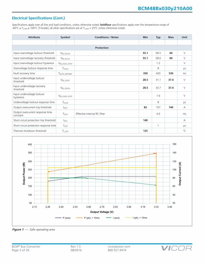
Output Voltage (V)
Out
put P
ower
(W)
P (ave) P (pk), < 10ms I (ave) I (pk), < 10ms
Out
put C
urre
nt (A
)
50
100
150
200
250
300
350
400
2.13 2.26 2.40 2.53 2.66 2.79 2.93 3.06 3.19 3.33 3.46
20
40
60
80
100
120
140
160
Figure 1 — Safe operating area
Electrical Specifications (Cont.)
Specifications apply over all line and load conditions, unless otherwise noted; boldface specifications apply over the temperature range of -40°C ≤ TCASE ≤ 100°C (T-Grade); all other specifications are at TCASE = 25ºC unless otherwise noted.
Attribute Symbol Conditions / Notes Min Typ Max Unit
Protection
Input overvoltage lockout threshold VIN_OVLO+ 55.1 58.5 60 V
Input overvoltage recovery threshold VIN_OVLO- 55.1 58.0 60 V
Input overvoltage lockout hysteresis VIN_OVLO_HYST 1.2 V
Overvoltage lockout response time TOVLO 8 µs
Fault recovery time TAUTO_RESTART 350 420 530 ms
Input undervoltage lockout threshold
VIN_UVLO- 28.5 31.1 37.4 V
Input undervoltage recovery threshold
VIN_UVLO+ 28.5 33.7 37.4 V
Input undervoltage lockout hysteresis
VIN_UVLO_HYST 1.6 V
Undervoltage lockout response time TUVLO 8 µs
Output overcurrent trip threshold IOCP 82 107 140 A
Output overcurrent response time constant
TOCP Effective internal RC filter 4.9 ms
Short circuit protection trip threshold ISCP 140 A
Short circuit protection response time TSCP 1 µs
Thermal shutdown threshold TJ_OTP 125 °C

BCM48Bx030y210A00
BCM® Bus Converter Rev 1.5 vicorpower.comPage 6 of 20 08/2016 800 927.9474
Signal Characteristics
Specifications apply over all line and load conditions, unless otherwise noted; boldface specifications apply over the temperature range of -40°C ≤ TCASE ≤ 100°C (T-Grade; all other specifications are at TCASE = 25ºC unless otherwise noted.
Primary Control: PC
• The PC pin enables and disables the BCM. When held low, the BCM is disabled.• In an array of BCM modules, PC pins should be interconnected to synchronize start up and permit start up into full load conditions.• PC pin outputs 5V during normal operation. PC pin internal bias level drops to 2.5V during fault mode, provided VIN remains in the valid range.
SIGNAL TYPE STATE ATTRIBUTE SYMBOL CONDITIONS / NOTES MIN TYP MAX UNIT
ANALOGOUTPUT
RegularOperation
PC voltage VPC 4.7 5.0 5.3 V
PC available current IPC_OP 2.0 3.5 5.0 mA
StandbyPC source (current) IPC_EN 50 100 µA
PC resistance (internal) RPC_INT Internal pull down resistor 50 150 400 kΩ
Transition PC capacitance (internal) CPC_INT 1000 pF
Start Up PC load resistance RPC_S To permit regular operation 60 kΩ
DIGITALINPUT / OUTPUT
RegularOperation
PC enable threshold VPC_EN 2.0 2.5 3.0 V
PC disable threshold VPC_DIS 1.95 V
Standby PC disable duration TPC_DIS_TMinimum time before attempting re-enable
1 s
Transition
PC threshold hysteresis VPC_HYSTER 50 mV
PC enable to VOUT time TON2 VIN = 48V for at least TON1 ms 50 100 150 µs
PC disable to standby time TPC_DIS 4 10 µs
PC fault response time TFR_PC From fault to PC = 2V 100 µs
Temperature Monitor: TM
• The TM pin monitors the internal temperature of the controller IC within an accuracy of ±5°C.• Can be used as a “Power Good” flag to verify that the BCM module is operating.• Is used to drive the internal comparator for Overtemperature Shutdown.
SIGNAL TYPE STATE ATTRIBUTE SYMBOL CONDITIONS / NOTES MIN TYP MAX UNIT
ANALOGOUTPUT
RegularOperation
TM voltage range VTM 2.12 4.04 V
TM voltage reference VTM_AMB TJ controller = 27°C 2.95 3.00 3.05 V
TM available current ITM 100 µA
TM gain ATM 10 mV/°C
TM voltage ripple VTM_PP CTM = 0pF, VIN = 48V, IOUT = 70A 120 200 mV
DIGITALINPUT / OUTPUT
TransitionTM capacitance (external) CTM_EXT 50 pF
TM fault response time TFR_TM From fault to TM = 1.5V 10 µs
StandbyTM voltage VTM_DIS 0 V
TM pull down (internal) RTM_INT Internal pull down resistor 25 40 50 kΩ
Reserved: RSV
Reserved for factory use. No connection should be made to this pin.

BCM48Bx030y210A00
BCM® Bus Converter Rev 1.5 vicorpower.comPage 7 of 20 08/2016 800 927.9474
Timing Diagram
12
34
56
V UVL
O+
PC 5 V
3 V
LL •
K
A: T
ON
1B:
TO
VLO
*C:
TAU
TO_R
ESTA
RTD
:TU
VLO
E: T
ON
2F:
TO
CPG
: TPC
–DIS
H: T
SCP*
*
1: C
ontr
olle
r sta
rt2:
Con
trol
ler t
urn
o�3:
PC
rele
ase
4: P
C pu
lled
low
5: P
C re
leas
ed o
n ou
tput
SC
6: S
C re
mov
ed
V OU
T
TM3
V @
27°
C
0.4
V
V IN 3
V5
V2.
5 V
500m
Sbe
fore
retr
ial
V UVL
O–
A
B
E
H
I SSP
I OU
T
I OCP
G
F
D
C
V OVL
O+
V O
VLO
–
V OVL
O+
NL
Not
es:
– T
imin
g an
d si
gnal
am
plitu
des
are
not t
o sc
ale
– E
rror
pul
se w
idth
is lo
ad d
epen
dent
*M
in v
alue
sw
itchi
ng o
�**
From
det
ectio
n of
err
or to
pow
er tr
ain
shut
dow
n
C

BCM48Bx030y210A00
BCM® Bus Converter Rev 1.5 vicorpower.comPage 8 of 20 08/2016 800 927.9474
Application Characteristics
The following values, typical of an application environment, are collected at TCASE = 25ºC unless otherwise noted. See associated figures for general trend data.
Input Voltage (V)
No
Load
Pow
er D
issi
patio
n (W
)
-40°C 100°CT :CASE 25°C
0123456789
10
38 40 42 44 46 47 49 51 53 55Case Temperature (°C)
Full
Load
Effi
cien
cy (%
)
38V 48V 55VV :IN
92
93
93
94
94
95
95
-40 -20 0 20 40 60 80 100
Load Current (A)
Effic
ienc
y (%
)
V :IN 38V 48V 55V
70
74
78
82
86
90
94
98
0 5 10 15 20 25 30 35 40 45 50 55 60 65 70
Figure 2 — No load power dissipation vs. Vin Figure 3 — Full load efficiency vs. temperature; Vin
Figure 4 — Efficiency at TCASE = -40°C
Load Current (A)
Effic
ienc
y (%
)
V :IN 38V 48V 55V
70
74
78
82
86
90
94
98
0 5 10 15 20 25 30 35 40 45 50 55 60 65 70
Figure 6 — Efficiency at TCASE = 25°C
Load Current (A)38V 48V 55VV :IN
Pow
er D
issi
patio
n (W
)
0 5 10 15 20 25 30 35 40 45 50 55 60 65 700
5
10
15
20
25
30
35
Figure 5 — Power dissipation at TCASE = -40°C
Load Current (A)
38V 48V 55VV :IN
Pow
er D
issi
patio
n (W
)
0 5 10 15 20 25 30 35 40 45 50 55 60 65 700
5
10
15
20
25
30
35
Figure 7 — Power dissipation at TCASE = 25°C

BCM48Bx030y210A00
BCM® Bus Converter Rev 1.5 vicorpower.comPage 9 of 20 08/2016 800 927.9474
Load Current (A)
Rip
ple
(mV
pk-p
k)
48 VV :IN
0255075
100125150175200225250
0 5 10 15 20 25 30 35 40 45 50 55 60 65 70
Figure 11 — Vripple vs. Iout: no external Cout, board mounted module, scope setting : 20MHz analog BW
Load Current (A)
Effic
ienc
y (%
)
V :IN 38V 48V 55V
70
74
78
82
86
90
94
98
0 5 10 15 20 25 30 35 40 45 50 55 60 65 70
Figure 8 — Efficiency at TCASE = 100°C
Case Temperature (°C)
RO
UT (
mΩ
)
I :OUT 35A 70A
0.5
0.8
1.0
1.3
1.5
1.8
2.0
-40 -20 0 20 40 60 80 100
Figure 10 — ROUT vs. temperature; nominal input
Load Current (A)38V 48V 55VV :IN
Pow
er D
issi
patio
n (W
)
0 5 10 15 20 25 30 35 40 45 50 55 60 65 700
5
10
15
20
25
30
35
Figure 9 — Power dissipation at TCASE = 100°C
Application Characteristics (Cont.)
BCM48Bx030y210A00
BCM® Bus Converter Rev 1.5 vicorpower.comPage 10 of 20 08/2016 800 927.9474
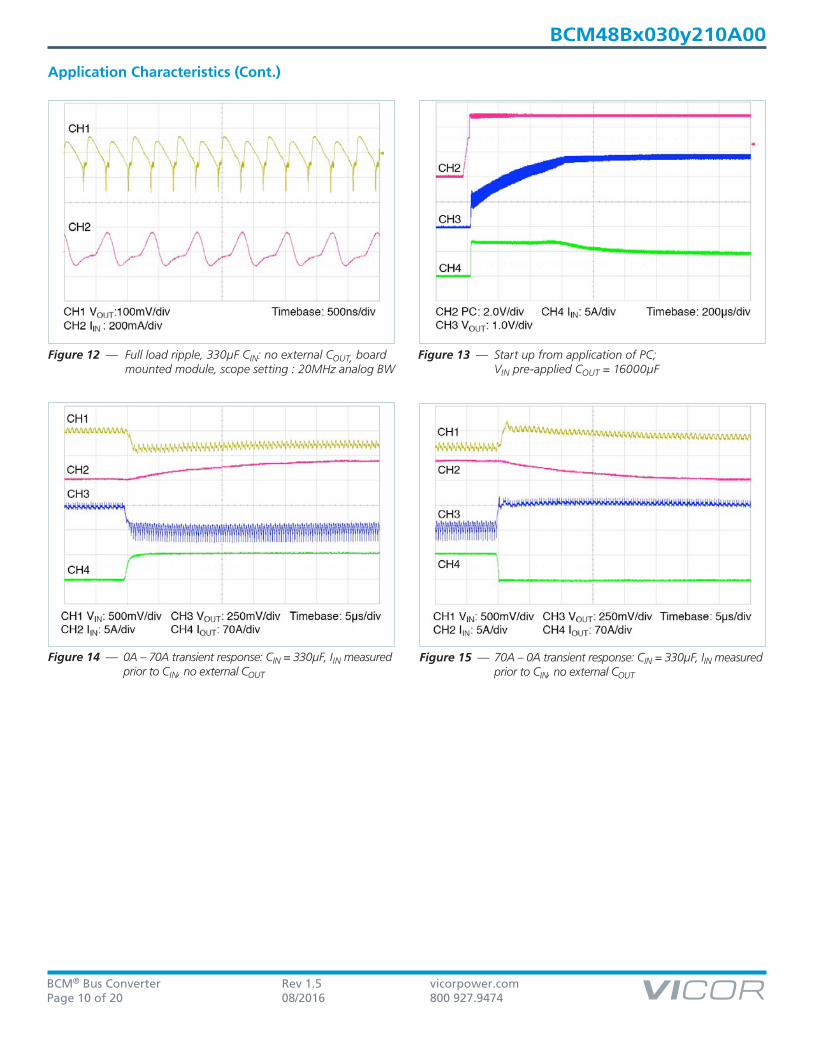
Figure 13 — Start up from application of PC; Vin pre-applied Cout = 16000µF
Figure 12 — Full load ripple, 330µF Cin: no external Cout, board mounted module, scope setting : 20MHz analog BW
Figure 15 — 70A – 0A transient response: Cin = 330µF, Iin measured prior to Cin, no external Cout
Figure 14 — 0A – 70A transient response: Cin = 330µF, Iin measured prior to Cin, no external Cout
Application Characteristics (Cont.)

BCM48Bx030y210A00
BCM® Bus Converter Rev 1.5 vicorpower.comPage 11 of 20 08/2016 800 927.9474
General Characteristics
Specifications apply over all line and load conditions, unless otherwise noted; boldface specifications apply over the temperature range of -40°C ≤ TCASE ≤ 100°C (T-Grade); all other specifications are at TCASE = 25ºC unless otherwise noted.
Attribute Symbol Conditions / Notes Min Typ Max Unit
Mechanical
Length L 32.25 / [1.270] 32.50 / [1.280] 32.75 / [1.289] mm / [in]
Width W 21.75 / [0.856] 22.00 / [0.866] 22.25 / [0.876] mm / [in]
Height H 6.48 / [0.255] 6.73 / [0.265] 6.98 / [0.275] mm / [in]
Volume Vol No heat sink 4.81 / [0.294] cm3/ [in3]
Weight W 14.5 / [0.512] g / [oz]
Lead Finish
Nickel 0.51 2.03
µmPalladium 0.02 0.15
Gold 0.003 0.051
Thermal
Operating temperature TJ
BCM48Bx030T210A00 (T-Grade) -40 125°C
BCM48Bx030M210A00 (M-Grade) -55 125
Thermal resistance fJC
Isothermal heatsink andisothermal internal PCB
1 °C/W
Thermal capacity 5 Ws/°C
Assembly
Peak compressive forceapplied to case (Z-axis)
Supported by J-lead only6 lbs
5.41 lbs/ in2
Storage Temperature
TST
BCM48Bx030T210A00 (T-Grade) -40 125 °C
BCM48Bx030M210A00 (M-Grade) -65 125 °C
ESD Withstand
ESDHBMHuman Body Model, “JEDEC JESD 22-A114D.01”Class 1D
1000
V
ESDCDMCharge Device Model, “JEDEC JESD 22-C101-D”
400
Soldering
Peak temperature during reflow MSL 4 (Datecode 1528 and later) 245 °C
Peak time above 217°C 60 90 s
Peak heating rate during reflow 1.5 3 °C/s
Peak cooling rate post reflow 1.5 6 °C/s
Safety
Working voltage (IN – OUT) VIN_OUT 60 VDC
Isolation voltage (hipot) VHIPOT 2,250 VDC
Isolation capacitance CIN_OUT Unpowered unit 2500 3200 3800 pF
Isolation resistance RIN_OUT At 500VDC 10 MΩ
MTBF
MIL-HDBK-217Plus Parts Count - 25°CGround Benign, Stationary, Indoors /Computer Profile
5.04 MHrs
Telcordia Issue 2 - Method I Case III;25°C Ground Benign, Controlled
6.35 MHrs
Agency approvals / standards
cTUVus
cURus
CE Marked for Low Voltage Directive and ROHS recast directive, as applicable.

BCM48Bx030y210A00
BCM® Bus Converter Rev 1.5 vicorpower.comPage 12 of 20 08/2016 800 927.9474
Using the Control Signals PC, TM
Primary Control (PC) pin can be used to accomplish the following functions:
n Logic enable and disable for module: Once TON1 time has been satisfied, a PC voltage greater than VPC_EN will cause the module to start. Bringing PC lower than VPC_DIS will cause the module to enter standby.
n Auxiliary voltage source: Once enabled in regular operational conditions (no fault), each BCM module PC provides a regulated 5V, 3.5mA voltage source.
n Synchronized start up: In an array of parallel modules, PC pins should be connected to synchronize start up across units. This permits the maximum load and capacitance to scale by the number of paralleled modules.
n Output disable: PC pin can be actively pulled down in order to disable the module. Pull down impedance shall be lower than 60Ω.
n Fault detection flag: The PC 5V voltage source is internally turned off as soon as a fault is detected.
n Note that PC can not sink significant current during a fault condition. The PC pin of a faulted module will not cause interconnected PC pins of other modules to be disabled.
Temperature Monitor (TM) pin provides a voltage proportional to the absolute temperature of the converter control IC.
It can be used to accomplish the following functions:
n Monitor the control IC temperature: The temperature in Kelvin is equal to the voltage on the TM pin scaled by 100. (i.e. 3.0V = 300K = 27ºC). If a heat sink is applied, TM can be used to protect the system thermally.
n Fault detection flag: The TM voltage source is internally turned off as soon as a fault is detected. For system monitoring purposes microcontroller interface faults are detected on falling edges of TM signal.

BCM48Bx030y210A00
BCM® Bus Converter Rev 1.5 vicorpower.comPage 13 of 20 08/2016 800 927.9474
The Sine Amplitude Converter (SAC™) uses a high frequency resonant tank to move energy from input to output. The resonant LC tank, operated at high frequency, is amplitude modulated as a function of input voltage and output current. A small amount of capacitance embedded in the input and output stages of the module is sufficient for full functionality and is key to achieving power density.
The BCM48Bx030y210A00 SAC can be simplified into the preceeding model.
At no load:
VOUT = VIN • K (1)
K represents the “turns ratio” of the SAC. Rearranging Eq (1):
K =
VOUT (2)
VIN
In the presence of load, VOUT is represented by:
VOUT = VIN • K – IOUT • ROUT (3)
and Iout is represented by:
IOUT =
IIN – IQ (4) K
ROUT represents the impedance of the SAC, and is a function of the Rdson of the input and output MOSFETs and the winding resistance of the power transformer. Iq represents the quiescent current of the SAC control, gate drive circuitry, and core losses.
The use of DC voltage transformation provides additional interesting attributes. Assuming that ROUT = 0Ω and IQ = 0A, Eq. (3) now becomes Eq. (1) and is essentially load independent, resistor R is now placed in series with VIN.
The relationship between VIN and VOUT becomes:
VOUT = (VIN – IIN • R) • K (5)
Substituting the simplified version of Eq. (4) (IQ is assumed = 0A) into Eq. (5) yields:
VOUT = VIN • K – IOUT • R • K2 (6)
R
SACK = 1/32Vin
Vout+–
VinVout
RSAC™
K = 1/16
Figure 17 — K = 1/16 Sine Amplitude Converter with series input resistor
Figure 16 — VI Chip® module AC model
+
–
+
–
VOUT
COUTVIN
V•I
K
+
–
+
–
CIN
IOUT
RCOUT
IQ
ROUT
RCIN
81mA
1/16 • Iout 1/16 • Vin
1.4mΩ
Rcin
0.57mΩ
218pH
0.2Ω Rcout
81µΩ
Lout = 600pH
3.2µF IQ
Lin = 5.7nH Iout
Rout
Vin Vout
CoutCin
Sine Amplitude Converter™ Point of Load Conversion
200µF
BCM48Bx030y210A00
BCM® Bus Converter Rev 1.5 vicorpower.comPage 14 of 20 08/2016 800 927.9474
This is similar in form to Eq. (3), where ROUT is used to represent the characteristic impedance of the SAC™. However, in this case a real R on the input side of the SAC is effectively scaled by K2 with respect to the output.
Assuming that R = 1Ω, the effective R as seen from the secondary side is 3.9mΩ, with K = 1/16.
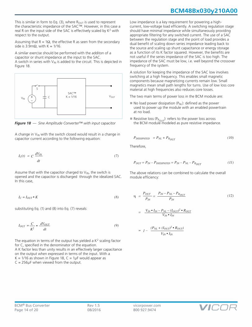
A similar exercise should be performed with the additon of a capacitor or shunt impedance at the input to the SAC. A switch in series with VIN is added to the circuit. This is depicted in Figure 18.
A change in VIN with the switch closed would result in a change in capacitor current according to the following equation:
IC(t) = C dVIN (7)
dt
Assume that with the capacitor charged to VIN, the switch is opened and the capacitor is discharged through the idealized SAC. In this case,
IC = IOUT • K (8)
substituting Eq. (1) and (8) into Eq. (7) reveals:
IOUT = C • dVOUT (9)
K2 dt
The equation in terms of the output has yielded a K2 scaling factor for C, specified in the denominator of the equation. A K factor less than unity results in an effectively larger capacitance on the output when expressed in terms of the input. With a K = 1/16 as shown in Figure 18, C = 1µF would appear as C = 256µF when viewed from the output.
Low impedance is a key requirement for powering a high-current, low-voltage load efficiently. A switching regulation stage should have minimal impedance while simultaneously providing appropriate filtering for any switched current. The use of a SAC between the regulation stage and the point of load provides a dual benefit of scaling down series impedance leading back to the source and scaling up shunt capacitance or energy storage as a function of its K factor squared. However, the benefits are not useful if the series impedance of the SAC is too high. The impedance of the SAC must be low, i.e. well beyond the crossover frequency of the system.
A solution for keeping the impedance of the SAC low involves switching at a high frequency. This enables small magnetic components because magnetizing currents remain low. Small magnetics mean small path lengths for turns. Use of low loss core material at high frequencies also reduces core losses.
The two main terms of power loss in the BCM module are:
n No load power dissipation (PNL): defined as the power used to power up the module with an enabled powertrain at no load.
n Resistive loss (PROUT): refers to the power loss across
the BCM module modeled as pure resistive impedance.
PDISSIPATED = PNL + PROUT (10) Therefore,
POUT = PIN – PDISSIPATED = PIN – PNL – PROUT (11)
The above relations can be combined to calculate the overall module efficiency:
h =
POUT =
PIN – PNL – PROUT (12) PIN PIN
= VIN • IIN – PNL – (IOUT)2 • ROUT VIN • IIN
= 1 –
(PNL + (IOUT)2 • ROUT) VIN • IIN
C
S
SACK = 1/32Vin
Vout+–
Figure 18 — Sine Amplitude Converter™ with input capacitor
VinVoutC
SAC™K = 1/16
S

BCM48Bx030y210A00
BCM® Bus Converter Rev 1.5 vicorpower.comPage 15 of 20 08/2016 800 927.9474
Input and Output Filter Design
A major advantage of SAC™ systems versus conventional PWM converters is that the transformers do not require large functional filters. The resonant LC tank, operated at extreme high frequency, is amplitude modulated as a function of input voltage and output current and efficiently transfers charge through the isolation transformer. A small amount of capacitance embedded in the input and output stages of the module is sufficient for full functionality and is key to achieve power density.
This paradigm shift requires system design to carefully evaluate external filters in order to:
1. Guarantee low source impedance:
To take full advantage of the BCM module’s dynamic response, the impedance presented to its input terminals must be low from DC to approximately 5MHz. The connection of the bus converter module to its power source should be implemented with minimal distribution inductance. If the interconnect inductance exceeds 100nH, the input should be bypassed with a RC damper to retain low source impedance and stable operation. With an interconnect inductance of 200nH, the RC damper may be as high as 1µF in series with 0.3Ω. A single electrolytic or equivalent low-Q capacitor may be used in place of the series RC bypass.
2. Further reduce input and/or output voltage ripple without sacrificing dynamic response:
Given the wide bandwidth of the module, the source response is generally the limiting factor in the overall system response. Anomalies in the response of the source will appear at the output of the module multiplied by its K factor. This is illustrated in Figures 14 and 15.
3. Protect the module from overvoltage transients imposed by the system that would exceed maximum ratings and cause failures:
The module input/output voltage ranges shall not be exceeded. An internal overvoltage lockout function prevents operation outside of the normal operating input range. Even during this condition, the powertrain is exposed to the applied voltage and power MOSFETs must withstand it. A criterion for protection is the maximum amount of energy that the input or output switches can tolerate if avalanched.
Total load capacitance at the output of the BCM module shall not exceed the specified maximum. Owing to the wide bandwidth and low output impedance of the module, low-frequency bypass capacitance and significant energy storage may be more densely and efficiently provided by adding capacitance at the input of the module. At frequencies <500kHz the module appears as an impedance of ROUT between the source and load.
Within this frequency range, capacitance at the input appears as effective capacitance on the output per the relationship defined in Eq. 13.
COUT = CIN (13)
K2
This enables a reduction in the size and number of capacitors used in a typical system.
Thermal Considerations
VI Chip® products are multi-chip modules whose temperature distribution varies greatly for each part number as well as with the input / output conditions, thermal management and environmental conditions. Maintaining the top of the BCM48Bx030y210A00 case to less than 100ºC will keep all junctions within the VI Chip module below 125ºC for most applications.
The percent of total heat dissipated through the top surface versus through the J-lead is entirely dependent on the particular mechanical and thermal environment. The heat dissipated through the top surface is typically 60%. The heat dissipated through the J-lead onto the PCB surface is typically 40%. Use 100% top surface dissipation when designing for a conservative cooling solution.
It is not recommended to use a VI Chip module for an extended period of time at full load without proper heat sinking.
BCM48Bx030y210A00
BCM® Bus Converter Rev 1.5 vicorpower.comPage 16 of 20 08/2016 800 927.9474
BCM®1R0_1
ZIN_EQ1 ZOUT_EQ1
ZOUT_EQ2
VOUT
ZOUT_EQn
ZIN_EQ2
ZIN_EQn
R0_2
R0_n
BCM®2
BCM®n
LoadDC
VIN
+
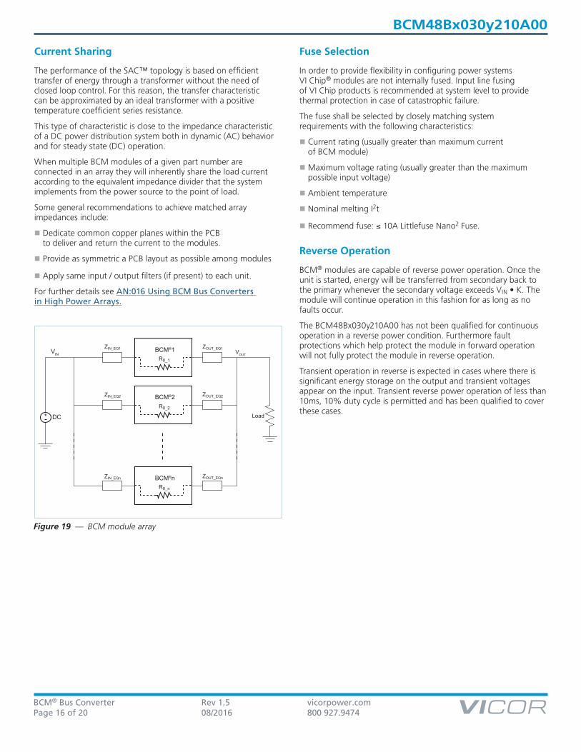
Figure 19 — BCM module array
Current Sharing
The performance of the SAC™ topology is based on efficient transfer of energy through a transformer without the need of closed loop control. For this reason, the transfer characteristic can be approximated by an ideal transformer with a positive temperature coefficient series resistance.
This type of characteristic is close to the impedance characteristic of a DC power distribution system both in dynamic (AC) behavior and for steady state (DC) operation.
When multiple BCM modules of a given part number are connected in an array they will inherently share the load current according to the equivalent impedance divider that the system implements from the power source to the point of load.
Some general recommendations to achieve matched array impedances include:
n Dedicate common copper planes within the PCB to deliver and return the current to the modules.
n Provide as symmetric a PCB layout as possible among modules
n Apply same input / output filters (if present) to each unit.
For further details see AN:016 Using BCM Bus Converters in High Power Arrays.
Fuse Selection
In order to provide flexibility in configuring power systems VI Chip® modules are not internally fused. Input line fusing of VI Chip products is recommended at system level to provide thermal protection in case of catastrophic failure.
The fuse shall be selected by closely matching system requirements with the following characteristics:
n Current rating (usually greater than maximum current of BCM module)
n Maximum voltage rating (usually greater than the maximum possible input voltage)
n Ambient temperature
n Nominal melting I2t
n Recommend fuse: ≤ 10A Littlefuse Nano2 Fuse.
Reverse Operation
BCM® modules are capable of reverse power operation. Once the unit is started, energy will be transferred from secondary back to the primary whenever the secondary voltage exceeds VIN • K. The module will continue operation in this fashion for as long as no faults occur.
The BCM48Bx030y210A00 has not been qualified for continuous operation in a reverse power condition. Furthermore fault protections which help protect the module in forward operation will not fully protect the module in reverse operation.
Transient operation in reverse is expected in cases where there is significant energy storage on the output and transient voltages appear on the input. Transient reverse power operation of less than 10ms, 10% duty cycle is permitted and has been qualified to cover these cases.
BCM48Bx030y210A00
BCM® Bus Converter Rev 1.5 vicorpower.comPage 17 of 20 08/2016 800 927.9474
inchmmNOTES:
1. DIMENSIONS ARE .2. UNLESS OTHERWISE SPECIFIED, TOLERANCES ARE: .X / [.XX] = +/-0.25 / [.01]; .XX / [.XXX] = +/-0.13 / [.005]3. PRODUCT MARKING ON TOP SURFACE
DXF and PDF files are available on vicorpower.com
inchmmNOTES:
1. DIMENSIONS ARE .2. UNLESS OTHERWISE SPECIFIED, TOLERANCES ARE: .X / [.XX] = +/-0.25 / [.01]; .XX / [.XXX] = +/-0.13 / [.005]3. PRODUCT MARKING ON TOP SURFACE
DXF and PDF files are available on vicorpower.com
inchmmNOTES:
1. DIMENSIONS ARE .2. UNLESS OTHERWISE SPECIFIED, TOLERANCES ARE: .X / [.XX] = +/-0.25 / [.01]; .XX / [.XXX] = +/-0.13 / [.005]3. PRODUCT MARKING ON TOP SURFACE
DXF and PDF files are available on vicorpower.com
inchmmNOTES:
1. DIMENSIONS ARE .2. UNLESS OTHERWISE SPECIFIED, TOLERANCES ARE: .X / [.XX] = +/-0.25 / [.01]; .XX / [.XXX] = +/-0.13 / [.005]3. PRODUCT MARKING ON TOP SURFACE
DXF and PDF files are available on vicorpower.com
J-Lead Package Recommended Land Pattern
mm(inch)
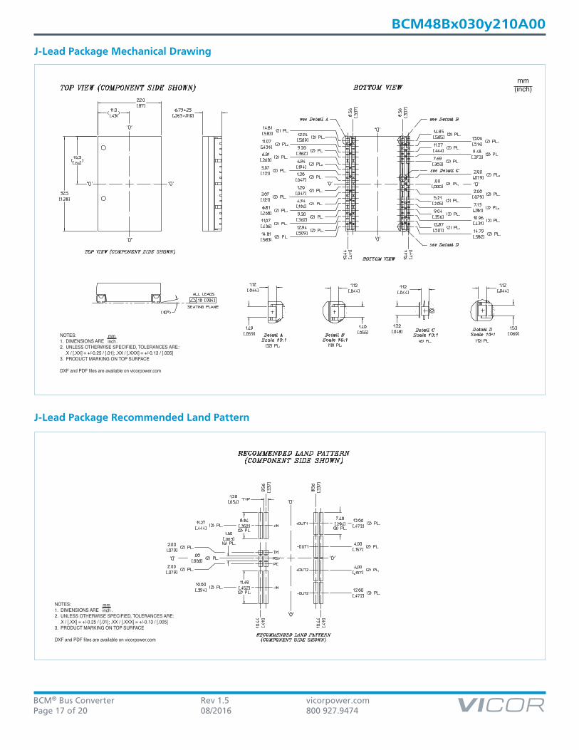
J-Lead Package Mechanical Drawing

BCM48Bx030y210A00
BCM® Bus Converter Rev 1.5 vicorpower.comPage 18 of 20 08/2016 800 927.9474
TOP VIEW ( COMPONENT SIDE )
BOTTOM VIEWNOTES: 1. DIMENSIONS ARE
2. UNLESS OTHERWISE SPECIFIED TOLERANCES ARE: X.X [X.XX] = ±0.25 [0.01]; X.XX [X.XXX] = ±0.13 [0.005]
3. RoHS COMPLIANT PER CST-0001 LATEST REVISION
DXF and PDF files are available on vicorpower.com
inch(mm)
.
NOTES: 1. DIMENSIONS ARE
2. UNLESS OTHERWISE SPECIFIED TOLERANCES ARE: X.X [X.XX] = ±0.25 [0.01]; X.XX [X.XXX] = ±0.13 [0.005]
3. RoHS COMPLIANT PER CST-0001 LATEST REVISION
DXF and PDF files are available on vicorpower.com
inch(mm)
.RECOMMENDED HOLE PATTERN
( COMPONENT SIDE SHOWN )
Through-Hole Package Recommended Land Pattern
mm(inch)
Through-Hole Package Mechanical Drawing

BCM48Bx030y210A00
BCM® Bus Converter Rev 1.5 vicorpower.comPage 19 of 20 08/2016 800 927.9474
Notes:
1. Maintain 3.50 (0.138) Dia. keep-out zone free of copper, all PCB layers.2. (A) Minimum recommended pitch is 39.50 (1.555). This provides 7.00 (0.275) component edge-to-edge spacing, and 0.50 (0.020) clearance between Vicor heat sinks. (B) Minimum recommended pitch is 41.00 (1.614). This provides 8.50 (0.334) component edge-to-edge spacing, and 2.00 (0.079) clearance between Vicor heat sinks.
3. VI Chip® module land pattern shown for reference only; actual land pattern may differ. Dimensions from edges of land pattern to push–pin holes will be the same for all full-size VI Chip® products.4. RoHS compliant per CST–0001 latest revision.
(NO GROUNDING CLIPS) (WITH GROUNDING CLIPS)
5. Unless otherwise specified: Dimensions are mm (inches) tolerances are: x.x (x.xx) = ±0.3 (0.01) x.xx (x.xxx) = ±0.13 (0.005)6. Plated through holes for grounding clips (33855) shown for reference, heat sink orientation and device pitch will dictate final grounding solution.
Recommended Heat Sink Push Pin Location

BCM48Bx030y210A00
BCM® Bus Converter Rev 1.5 vicorpower.comPage 20 of 20 08/2016 800 927.9474
Vicor’s comprehensive line of power solutions includes high density AC-DC and DC-DC modules and ac-cessory components, fully configurable AC-DC and DC-DC power supplies, and complete custom power systems.
Information furnished by Vicor is believed to be accurate and reliable. However, no responsibility is assumed by Vicor for its use. Vicor makes no representations or warranties with respect to the accuracy or completeness of the contents of this publication. Vicor reserves the right to make changes to any products, specifications, and product descriptions at any time without notice. Information published by Vicor has been checked and is believed to be accurate at the time it was printed; however, Vicor assumes no responsibility for inaccuracies. Testing and other quality controls are used to the extent Vicor deems necessary to support Vicor’s product warranty. Except where mandated by government requirements, testing of all parameters of each product is not necessarily performed. Specifications are subject to change without notice.
Vicor’s Standard Terms and ConditionsAll sales are subject to Vicor’s Standard Terms and Conditions of Sale, which are available on Vicor’s webpage or upon request.
Product WarrantyIn Vicor’s standard terms and conditions of sale, Vicor warrants that its products are free from non-conformity to its Standard Specifications (the “Express Limited Warranty”). This warranty is extended only to the original Buyer for the period expiring two (2) years after the date of shipment and is not transferable. UNLESS OTHERWISE EXPRESSLY STATED IN A WRITTEN SALES AGREEMENT SIGNED BY A DULY AUTHORIZED VICOR SIGNATORY, VICOR DIS-CLAIMS ALL REPRESENTATIONS, LIABILITIES, AND WARRANTIES OF ANY KIND (WHETHER ARISING BY IMPLICATION OR BY OPERATION OF LAW) WITH RESPECT TO THE PRODUCTS, INCLUDING, WITHOUT LIMITATION, ANY WARRANTIES OR REPRESENTATIONS AS TO MERCHANTABILITY, FITNESS FOR PARTICULAR PURPOSE, INFRINGEMENT OF ANY PATENT, COPYRIGHT, OR OTHER INTELLECTUAL PROPERTY RIGHT, OR ANY OTHER MATTER.
This warranty does not extend to products subjected to misuse, accident, or improper application, maintenance, or storage. Vicor shall not be liable for collateral or consequential damage. Vicor disclaims any and all liability arising out of the application or use of any product or circuit and assumes no liability for applications assistance or buyer product design. Buyers are responsible for their products and applications using Vicor products and components. Prior to using or distributing any products that include Vicor components, buyers should provide adequate design, testing and operat-ing safeguards.
Vicor will repair or replace defective products in accordance with its own best judgment. For service under this warranty, the buyer must contact Vicor to obtain a Return Material Authorization (RMA) number and shipping instructions. Products returned without prior authorization will be returned to the buyer. The buyer will pay all charges incurred in returning the product to the factory. Vicor will pay all reshipment charges if the product was defective within the terms of this warranty.
Life Support PolicyVICOR’S PRODUCTS ARE NOT AUTHORIZED FOR USE AS CRITICAL COMPONENTS IN LIFE SUPPORT DEVICES OR SYSTEMS WITHOUT THE EXPRESS PRIOR WRITTEN APPROVAL OF THE CHIEF EXECUTIVE OFFICER AND GENERAL COUNSEL OF VICOR CORPORATION. As used herein, life support devices or systems are devices which (a) are intended for surgical implant into the body, or (b) support or sustain life and whose failure to perform when properly used in accordance with instructions for use provided in the labeling can be reasonably expected to result in a significant injury to the user. A critical component is any component in a life support device or system whose failure to perform can be reasonably expected to cause the failure of the life support device or system or to affect its safety or effectiveness. Per Vicor Terms and Conditions of Sale, the user of Vicor products and components in life support applications assumes all risks of such use and indemnifies Vicor against all liability and damages.
Intellectual Property NoticeVicor and its subsidiaries own Intellectual Property (including issued U.S. and Foreign Patents and pending patent applications) relating to the products described in this data sheet. No license, whether express, implied, or arising by estoppel or otherwise, to any intellectual property rights is granted by this document. Interested parties should contact Vicor’s Intellectual Property Department.
The products described on this data sheet are protected by the following U.S. Patents Numbers:5,945,130; 6,403,009; 6,710,257; 6,911,848; 6,930,893; 6,934,166; 6,940,013; 6,969,909; 7,038,917; 7,145,186; 7,166,898; 7,187,263; 7,202,646; 7,361,844; D496,906; D505,114; D506,438; D509,472; and for use under 6,975,098 and 6,984,965.
Vicor Corporation25 Frontage Road
Andover, MA, USA 01810Tel: 800-735-6200Fax: 978-475-6715
emailCustomer Service: [email protected]
Technical Support: [email protected]