bcm bus converter - vicor · digital supervisor and i13tl1a0 digital isolator, ... in = 400 v ( 260...
TRANSCRIPT
BCM® Bus Converter Rev 1.3 vicorpower.comPage 1 of 23 05/2015 800 927.9474
BCM® Bus Converter
Fixed Ratio DC-DC Converter
BCM400y500x1K8A31
Features
• Up to 1750 W continuous output power
• 2735 W/in3 power density
• 98.0 % peak efficiency
• 4242 Vdc isolation
• Parallel operation for multi-kW arrays
• OV, OC, UV, short circuit and thermal protection
• 6123 through-hole ChiP package
n 2.494 ” x 0.898 ” x 0.286 ”
( 63.34 mm x 22.80 mm x 7.26 mm)
• PMBusTM management interface*
Typical Applications
• 380 DC Power Distribution
• High End Computing Systems
• Automated Test Equipment
• Industrial Systems
• High Density Power Supplies
• Communications Systems
• Transportation
Product Description
The VI Chip® Bus Converter (BCM) is a high efficiency SineAmplitude Converter (SAC), operating from a 260 to 410 VDCprimary bus to deliver an isolated ratiometric output from 32.5 to 51.3 VDC.
The BCM400y500x1K8A31 offers low noise, fast transientresponse, and industry leading efficiency and power density. Inaddition, it provides an AC impedance beyond the bandwidthof most downstream regulators, allowing input capacitancenormally located at the input of a POL regulator to be located atthe input of the BCM module. With a K factor of 1/8 , thatcapacitance value can be reduced by a factor of 64 x, resultingin savings of board area, material and total system cost.
The BCM400y500x1K8A31 , combined with the D44TL1A0Digital Supervisor and I13TL1A0 Digital Isolator, provide asecondary referenced PMBus™ compatible telemetry andcontrol interface. This interface provides access to the BCM’sinternal controller configuration, fault monitoring, and othertelemetry functions.
Leveraging the thermal and density benefits of Vicor’s ChiPpackaging technology, the BCM module offers flexible thermalmanagement options with very low top and bottom sidethermal impedances. Thermally-adept ChiP-based powercomponents, enable customers to achieve low cost powersystem solutions with previously unattainable system size,weight and efficiency attributes, quickly and predictably.
Product Ratings
VIN = 400 V ( 260 – 410 V) POUT = up to 1750 W
VOUT = 50 V ( 32.5 – 51.3 V)(NO LOAD)
K = 1/8
*When used with D44TL1A0 and I13TL1A0 chipset
C US® S
NRTLC US
BCM® Bus Converter Rev 1.3 vicorpower.comPage 2 of 23 05/2015 800 927.9474
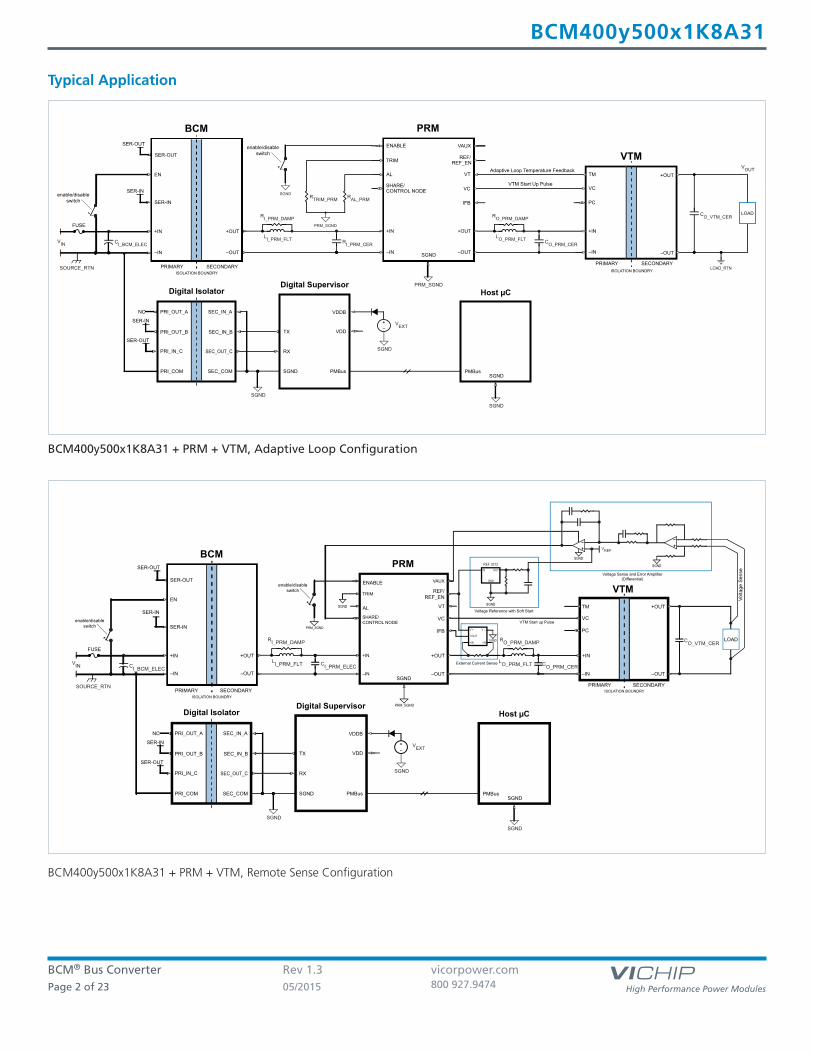
BCM400y500x1K8A31 Typical Application
BCM400y500x1K8A31 + PRM + VTM, Remote Sense Configuration
BCM400y500x1K8A31 + PRM + VTM, Adaptive Loop Configuration
External Current Sense
SGND
SGND
Voltage Reference with Soft Start
Voltage Sense and Error Amplifier(Differential)
VTM Start up Pulse
SGND
IN OUT
GND
V +
VOUT
–IN+IN
V –
PRM
ENABLE
TRIM
SHARE/CONTROL NODE
AL
IFB
VC
VT
VAUX
REF/REF_EN
+IN
–IN
+OUT
–OUT
PRM_SGND
SGND
TM
VC
PC
+IN
–IN –OUT
+OUT
ISOLATION BOUNDRY
VTM
PRIMARY SECONDARY
REF 3312 SGND
Vol
tage
Sen
se
SGND
LOAD
BCM
SER-IN
EN
+IN
–IN
+OUT
–OUT
enable/disableswitch
FUSE
ISOLATION BOUNDRY
PRIMARY SECONDARY
SER-OUT
VIN C
I_BCM_ELEC
SOURCE_RTN
PRM_SGND
CI_PRM_ELEC
RI_PRM_DAMP
LI_PRM_FLT
RO_PRM_DAMP
LO_PRM_FLT C
O_PRM_CER
CO_VTM_CER
VREF
enable/disableswitch
PRI_OUT_A
PRI_COM
SEC_IN_A
SEC_OUT_C
Digital SupervisorDigital Isolator
VDDB
VDDTX
RX
PMBusSGND
t
Host μC
SEC_COM PMBus
SGND
+
– V
EXT
PRI_IN_C
SEC_IN_B
SER-IN
PRI_OUT_B
SER-OUT
NC
SGND
SGND
SGND
SER-OUT
SER-IN
PRM
ENABLE
TRIM
SHARE/CONTROL NODE
AL
IFB
VC
VT
VAUX
REF/REF_EN
+IN
–IN
+OUT
–OUT
TM
VC
PC
+IN
–IN –OUT
+OUTAdaptive Loop Temperature Feedback
VTM Start Up Pulse
PRM_SGND
SGND
SGND
ISOLATION BOUNDRYLOAD_RTN
VTM
PRIMARY SECONDARY
BCM
SER-IN
EN
+IN
–IN
+OUT
–OUT
enable/disableswitch
FUSE
ISOLATION BOUNDRY
PRIMARY SECONDARY
SER-OUT
RI_PRM_CER
RTRIM_PRM
RAL_PRM
PRM_SGND
CI_BCM_ELEC
SOURCE_RTN
VIN
RI_PRM_DAMP
LI_PRM_FLT
RO_PRM_DAMP
LO_PRM_FLT
CO_PRM_CER
LOAD
VOUT
CO_VTM_CER
enable/disableswitch
PRI_OUT_A
PRI_COM
SEC_IN_A
SEC_OUT_C
Digital SupervisorDigital Isolator
VDDB
VDDTX
RX
PMBusSGND
t
Host μC
SEC_COM PMBus
SGND
+
– V
EXT
PRI_IN_C
SEC_IN_BPRI_OUT_B
NC
SGND
SGND
SGND
SER-OUT
SER-IN
SER-IN
SER-OUT

BCM® Bus Converter Rev 1.3 vicorpower.comPage 3 of 23 05/2015 800 927.9474
BCM400y500x1K8A31
1 2
A
B
C
D
E D’
C’
B’
+IN +OUT
TOP VIEW
6123 ChiP Package
A’
SER-IN
EN
+OUT
-OUT
-OUT-IN
SER-OUT
Pin Configuration
Pin Descriptions
Pin Number Signal Name Type Function
A1 +IN INPUT POWER Positive input power terminal
B1 SER-OUT OUTPUT UART transmit pin; Primary side referenced signals
C1 EN INPUT Enables and disables power supply; Primary side referenced signals
D1 SER-IN INPUT UART receive pin; Primary side referenced signals
E1 -ININPUT POWER
RETURNNegative input power terminal
A’2, C’2 +OUT OUTPUT POWER Positive output power terminal
B’2, D’2 -OUTOUTPUT POWER
RETURNNegative output power terminal

BCM® Bus Converter Rev 1.3 vicorpower.comPage 4 of 23 05/2015 800 927.9474
BCM400y500x1K8A31
Absolute Maximum RatingsThe absolute maximum ratings below are stress ratings only. Operation at or beyond these maximum ratings can cause permanent damage to the device.
Parameter Comments Min Max Unit
+IN to –IN -1 480 V
VIN slew rate (operational) 1000 V/ms
Isolation voltage, input to output Dielectric test applied to 100% production units 4242 V
+OUT to –OUT -1 60 V
SER-OUT to –IN -0.3 4.6 V
EN to –IN -0.3 5.5 V
SER-IN to –IN -0.3 4.6 V
Part Ordering Information
DeviceInput Voltage
RangePackage Type
OutputVoltage x 10
TemperatureGrade
OutputPower
RevisionPackage
SizeVersion
BCM 400 y 500 x 1K8 A 3 1
BCM = BCM 400 = 260 to 410 V P = ChiP Through Hole 500 = 50 VT = -40 to 125°CM = -55 to 125°C
1K8 = 1,750 W A 3 = 6123 1
Standard Models
All products shipped in JEDEC standard high profile (0.400” thick) trays (JEDEC Publication 95, Design Guide 4.10).
Part Number VIN Package Type VOUT Temperature Power Package Size
BCM 400 P 500 T 1K8 A31 260 to 410 V ChiP Through Hole 50 V
32.5 to 51.3 V-40°C to 125°C 1,750 W 6123
BCM 400 P 500 M 1K8 A31 260 to 410 V ChiP Through Hole 50 V
32.5 to 51.3 V-55°C to 125°C 1,750 W 6123

BCM® Bus Converter Rev 1.3 vicorpower.comPage 5 of 23 05/2015 800 927.9474
BCM400y500x1K8A31 Electrical Specifications
Specifications apply over all line and load conditions, unless otherwise noted; Boldface specifications apply over the temperature range of -40 °C ≤ TINTERNAL
≤ 125 °C (T-Grade); All other specifications are at TINTERNAL = 25 ºC unless otherwise noted.
Attribute Symbol Conditions / Notes Min Typ Max Unit
PowertrainInput voltage range, continuous VIN_DC 260 410 V
Input voltage range, transient VIN_TRANSFull current or power supported, 50 ms max,
260 410 V10% duty cycle max
VIN µController Active VµC_ACTIVEVIN voltage where µC is initialized,
120 V(ie VAUX = Low, powertrain inactive)
Quiescent current IQDisabled, EN Low, VIN = 400 V 2
mATINTERNAL ≤ 100ºC 4
No load power dissipation PNL
VIN = 400 V, TINTERNAL = 25 ºC 10 14
WVIN = 400 V 6 21
VIN = 260 V to 410 V, TINTERNAL = 25 ºC 15
VIN = 260 V to 410 V 22
Inrush current peak IINR_P
VIN = 410 V, COUT = 100 µF, 6 RLOAD = 25% of full load current A
TINTERNAL ≤ 100ºC 12
DC input current IIN_DC At POUT= 1750 W, TINTERNAL ≤ 100ºC 4.5 A
Transformation ratio K K = VOUT/ VIN, at no load 1/8 V/V
Output power (continuous) POUT_DC 1750 W
Output power (pulsed) POUT_PULSE 10 ms pulse, 25% Duty cycle, PTOTAL = % rated POUT_DC 2000 W
Output current (continuous) IOUT_DC 35 A
Output current (pulsed) IOUT_PULSE 10 ms pulse, 25% Duty cycle, ITOTAL = % rated IOUT_DC 40 A
VIN = 400 V, IOUT = 35 A 96.9 97.4
Efficiency (ambient) hAMB VIN = 260 V to 410 V, IOUT = 35 A 95.7 %
VIN = 400 V, IOUT = 17.50 A 97.5 98
Efficiency (hot) hHOT VIN = 400 V, IOUT = 35 A, TINTERNAL = 100 °C 96.3 96.8 %
Efficiency (over load range) h20% 7 A < IOUT < 35 A, TINTERNAL ≤ 100ºC 92 %
ROUT_COLD VIN = 400 V, IOUT = 35 A, TINTERNAL = -40 °C 12 16 20
Output resistance ROUT_AMB VIN = 400 V, IOUT = 35 A 16 22.6 33 mΩROUT_HOT VIN = 400 V, IOUT = 35 A, TINTERNAL = 100 °C 24 31 39
Switching frequency FSW Frequency of the Output Voltage Ripple = 2x FSW 1.05 1.10 1.14 MHz
COUT = 0 F, IOUT = 35 A, VIN = 400 V, 250
Output voltage ripple VOUT_PP 20 MHz BW mV
TINTERNAL ≤ 100ºC 350
Input inductance (parasitic) LIN_PARFrequency 2.5 MHz (double switching frequency),
6.7 nHSimulated lead model
Output inductance (parasitic) LOUT_PARFrequency 2.5 MHz (double switching frequency),
1.3 nHSimulated lead model
Input Series inductance (internal) LIN_INTReduces the need for input decoupling
0.56 µHinductance in BCM arrays
Effective Input capacitance (internal) CIN_INT Effective value at 400 VIN 0.37 µF

BCM® Bus Converter Rev 1.3 vicorpower.comPage 6 of 23 05/2015 800 927.9474
BCM400y500x1K8A31
Attribute Symbol Conditions / Notes Min Typ Max Unit
Powertrain (Cont.)Effective Output capacitance (internal) COUT_INT Effective value at 50 VOUT 25.6 µF
Effective Output capacitance (external) COUT_EXTExcessive capacitance may drive module into
0 100 µFSC protection
Array Maximum external output COUT_AEXT COUT_AEXT Max = N * 0.5*COUT_EXT Max
capacitance
Powertrain Protection
Startup into a persistent fault condition. 292.5 357.5 ms
Auto Restart Time tAUTO_RESTART Non-Latching fault detection given VIN > VIN_UVLO+,
Module will ignore attempts to re-enable during time off
Input overvoltage lockout threshold VIN_OVLO+ 430 440 450 V
Input overvoltage recovery threshold VIN_OVLO- 420 430 440 V
Input overvoltage lockout hysteresis VIN_OVLO_HYST 10 V
Overvoltage lockout response time tOVLO 10 µs
Soft-Start time tSOFT-STARTFrom powertrain active
1 msFast Current limit protection disabled during Soft-Start
Output overcurrent trip threshold IOCP 37.5 47 59 A
Overcurrent Response Time Constant tOCP Effective internal RC filter 3.6 ms
Short circuit protection trip threshold ISCP 52 A
Short circuit protection response time tSCP 1 µs
Overtemperature shutdown threshold tOTP Temperature sensor located inside controller IC 125 ºC
Powertrain Supervisory Limits
Input overvoltage lockout threshold VIN_OVLO+ 420 436 450 V
Input overvoltage recovery threshold VIN_OVLO- 405 426 440 V
Input overvoltage lockout hysteresis VIN_OVLO_HYST 10 V
Overvoltage lockout response time tOVLO 100 µs
Input undervoltage lockout threshold VIN_UVLO- 200 226 250 V
Input undervoltage recovery threshold VIN_UVLO+ 225 244 259 V
Input undervoltage lockout hysteresis VIN_UVLO_HYST 15 V
Undervoltage lockout response time tUVLO 100 µs
From VIN = VIN_UVLO+ to powertrain active,
Undervoltage startup delay tUVLO+_DELAY EN floating, (i.e One time Startup delay from 20 ms
application of VIN to VOUT)
Output Overcurrent Trip Threshold IOCP 42.5 45 47.5 A
Overcurrent Response Time Constant tOCP 2 ms
Overtemperature shutdown threshold tOTP Temperature sensor located inside controller IC 125 ºC
Undertemperature shutdown threshold tUTP Temperature sensor located inside controller IC -45 ºC
Undertemperature restart time tUTP_RESTARTStartup into a persistent fault condition. Non-Latching
3 sfault detection given VIN > VIN_UVLO+
Electrical Specifications (Cont.)
Specifications apply over all line and load conditions, unless otherwise noted; Boldface specifications apply over the temperature range of -40 °C ≤ TINTERNAL
≤ 125 °C (T-Grade); All other specifications are at TINTERNAL = 25 ºC unless otherwise noted.

BCM® Bus Converter Rev 1.3 vicorpower.comPage 7 of 23 05/2015 800 927.9474
BCM400y500x1K8A31
Ou
tpu
t C
urr
en
t (A
)
Input Voltage (V)
I (ave) I (pk), t < 10 ms
16 18 20 22 24 26 28 30 32 34 36 38 40 42
260 275 290 305 320 335 350 365 380 395 410
Ou
tpu
t P
ow
er
(W)
Input Voltage (V)
P (ave) P (pk), t < 10 ms
700 800 900
1000 1100 1200 1300 1400 1500 1600 1700 1800 1900 2000 2100
260 275 290 305 320 335 350 365 380 395 410
Figure 1 — Specified thermal operating area
Figure 2 — Specified electrical operating area using rated ROUT_HOT
0
10
20
30
40
50
60
70
80
90
100
110
0 10 20 30 40 50 60 70 80 90 100 110
Ou
tpu
t C
ap
acit
an
ce
(% R
ate
d C
OU
T M
AX
)
Load Current (% IOUT_AVG
)
Ou
tpu
t P
ow
er
(W)
Case Temperature (°C)
One side cooling One side cooling and leads Double Sided cooling and leads
0
200
400
600
800
1000
1200
1400
1600
1800
2000
35 45 55 65 75 85 95 105 115 125
Figure 3 — Specified Primary start-up into load current and external capacitance

BCM® Bus Converter Rev 1.3 vicorpower.comPage 8 of 23 05/2015 800 927.9474
BCM400y500x1K8A31 Reported Characteristics
Specifications apply over all line, load conditions, unless otherwise noted; Boldface specifications apply over the temperature range of -40 °C ≤ TINTERNAL
≤ 125 °C (T-Grade); All other specifications are at TINTERNAL = 25 ºC unless otherwise noted.
Monitored Telemetry
• The BCM communication version is not intended to be used without a Digital Supervisor.
ATTRIBUTEDIGITAL SUPERVISOR
PMBusTM READ COMMAND
ACCURACY(RATED RANGE)
FUNCTIONALREPORTING RANGE
UPDATE
RATEREPORTED UNITS
Input voltage (88h) READ_VIN ± 5% ( LL - HL ) 130 V to 450 V 100 µs VACTUAL = VREPORTED x 10-1
Input current (89h) READ_IIN ± 5% ( 10 - 133% of FL) - 0.85 A to 5.9 A 100 µs IACTUAL = IREPORTED x 10-3
Output voltage[1] (8Bh) READ_VOUT ± 5% ( LL - HL ) 16.25 V to 56.25 V 100 µs VACTUAL = VREPORTED x 10-1
Output current (8Ch) READ_IOUT ± 5% ( 10 - 133% of FL ) - 7 A to 47.5 A 100 µs IACTUAL = IREPORTED x 10-2
Output resistance (D4h) READ_ROUT ± 5% ( 50 - 100% of FL) 10 µΩ to 40 µΩ 100 ms RACTUAL = RREPORTED x 10-5
Temperature[2] (8Dh) READ_TEMPERATURE_1 ± 7°C ( Full Range) - 55ºC to 130ºC 100 ms TACTUAL = TREPORTED
Variable Parameter
• Factory setting of all below Thresholds and Warning limits are 100% of listed protection values.• Variables can be written only when module is disabled either EN pulled low or VIN < VIN_UVLO-.• Module must remain in a disabled mode for 3 ms after any changes to the below variables allowing ample time to commit changes to EEPROM.
ATTRIBUTEDIGITAL SUPERVISOR
PMBusTM COMMAND [3]CONDITIONS / NOTES
ACCURACY(RATED RANGE)
FUNCTIONALREPORTING
RANGE
DEFAULT
VALUE
Input / Output OvervoltageProtection Limit
(55h) VIN_OV_FAULT_LIMIT VIN_OVLO- is automatically 3%lower than this set point
± 5% ( LL - HL ) 130 V to 435 V 100%
Input / Output OvervoltageWarning Limit
(57h) VIN_OV_WARN_LIMIT ± 5% ( LL - HL ) 130 V to 435 V 100%
Input / Output UndervoltageProtection Limit
(D7h) DISABLE_FAULTS Can only be disabled to a presetdefault value
± 5% ( LL - HL ) 130 V or 260 V 100%
Input OvercurrentProtection Limit
(5Bh) IIN_OC_FAULT_LIMIT ± 5% ( 10 - 133% of FL) 0 to 5.625 A 100%
Input OvercurrentWarning Limit
(5Dh) IIN_OC_WARN_LIMIT ± 5% ( 10 - 133% of FL) 0 to 5.625 A 100%
Overtemperature ProtectionLimit
(4Fh) OT_FAULT_LIMIT ± 7°C ( Full Range) 0 to 125°C 100%
OvertemperatureWarning Limit
(51h) OT_WARN_LIMIT ± 7°C ( Full Range) 0 to 125°C 100%
Turn on Delay (60h) TON_DELAY Additional time delay to theUndervoltage Startup Delay
± 50 µs 0 to 100 ms 0 ms
[3] Refer to Digital Supervisor datasheet for complete list of supported commands.
[1] Default READ Output Voltage returned when unit is disabled = -300 V.[2] Default READ Temperature returned when unit is disabled = -273°C.

BCM® Bus Converter Rev 1.3 vicorpower.comPage 9 of 23 05/2015 800 927.9474
BCM400y500x1K8A31 Signal Characteristics
Specifications apply over all line, load conditions, unless otherwise noted; Boldface specifications apply over the temperature range of -40 °C ≤ TINTERNAL
≤ 125 °C (T-Grade); All other specifications are at TINTERNAL = 25 ºC unless otherwise noted.
UART SER-IN / SER-OUT Pins
• Universal Asynchronous Receiver/Transmitter (UART) pins.• The BCM communication version is not intended to be used without a Digital Supervisor. • Isolated I2C communication and telemetry is available when using Vicor Digital Isolator and Vicor Digital Supervisor. Please see specific product data sheet
for more details. • UART SER-IN pin is internally pulled high using a 1.5 kΩ to 3.3 V.
SIGNAL TYPE STATE ATTRIBUTE SYMBOL CONDITIONS / NOTES MIN TYP MAX UNIT
GENERAL I/O
Regular
Operation
Baud Rate BRUART Rate 750 Kbit/s
DIGITAL
INPUT
SER-IN Pin
SER-IN Input Voltage RangeVSER-IN_IH 2.3 V
VSER-IN_IL 1 V
SER-IN rise time tSER-IN_RISE 10% to 90% 400 ns
SER-IN fall time tSER-IN_FALL 10% to 90% 25 ns
SER-IN RPULLUP RSER-IN_PLP Pull up to 3.3 V 1.5 kΩ
SER-IN External Capacitance CSER-IN_EXT 400 pF
DIGITAL
OUTPUT
SER-OUT Pin
SER-OUT Output Voltage
Range
VSER-OUT_OH 0 mA ≥ IOH ≥ -4 mA 2.8 V
VSER-OUT_OL 0 mA ≤ IOL ≤ 4 mA 0.5 V
SER-OUT rise time tSER-OUT_RISE 10% to 90% 55 ns
SER-OUT fall time tSER-OUT_FALL 10% to 90% 45 ns
SER-OUT source current ISER-OUT VSER-OUT = 2.8 V 6 mA
SER-OUT output impedance ZSER-OUT 120 Ω
Enable / Disable Control
• The EN pin is a standard analog I/O configured as an input to an internal µC.• It is internally pulled high to 3.3 V.• When held low the BCM internal bias will be disabled and the powertrain will be inactive.• In an array of BCMs, EN pins should be interconnected to synchronize startup and permit startup into full load conditions.• Enable / disable command will have no effect if the EN pin is disabled.
SIGNAL TYPE STATE ATTRIBUTE SYMBOL CONDITIONS / NOTES MIN TYP MAX UNIT
ANALOG
INPUT
Startup EN to Powertrain active time tEN_START
VIN > VIN_UVLO+,EN held low both conditions satisfiedfor t > tUVLO+_DELAY
250 µs
Regular
Operation
EN Voltage Threshold VENABLE 2.3 V
EN Resistance (Internal) REN_INT Internal pull up resistor 1.5 kΩ
EN Disable Threshold VEN_DISABLE_TH 1 V

BCM® Bus Converter Rev 1.3 vicorpower.comPage 10 of 23 05/2015 800 927.9474
BCM400y500x1K8A31 BCM Module Timing diagram
EN+IN
BIDI
R
INPU
T
V OU
T
INPUT VOLT
AGE TURN-ON
OUTPUT TURN-ON IN
PUT OVER VOLTAGE
INPUT REST
ARTENABLE
PULLED LO
W
ENABLE PULLE
D HIGH SHORT CIRCUIT EVENT IN
PUT VOLTAGE TURN-O
FF
OU
TPU
T
EN & SE
R-ININ
TERNAL Pull-u
p
µcINITIALIZ
E
VIN
_OV
LO-
VIN
_OV
LO+
VIN
_UV
LO+
Vμ
C
VN
OM
VIN
_UV
LO
-
t SC
Pt U
VL
O+
_DE
LAY
t AU
TO
-RE
ST
AR
Tt W
AIT
≥ t E
NA
BLE
_OF
F
STAR
TUP
OVE
R VO
LTAG
EEN
ABLE
CO
NTR
OL O
VER
CURR
ENT
SHU
TDO
WN

BCM® Bus Converter Rev 1.3 vicorpower.comPage 11 of 23 05/2015 800 927.9474
BCM400y500x1K8A31
FAULT
SEQUENCE
EN High
Powertrain Stopped
VμC
< VIN
< VIN_UVLO+
VIN
> VIN_UVLO+
tUVLO+_DELAY
expired
ONE TIME DELAY
INITIAL STARTUPFault
Auto-
recovery
ENABLE falling edge,
or OTP detected
Input OVLO or UVLO,
Output OCP,
or UTP detected
ENABLE falling edge,
or OTP detected
Input OVLO or UVLO,
Output OCP,
or UTP detected
Short Circuit detected
Application
of VIN
SUSTAINED
OPERATION
EN High
Powertrain Active
STARTUP SEQUENCE
EN High
Powertrain Stopped
STANDBY SEQUENCE
EN High
Powertrain Stopped
High Level Functional State Diagram
Conditions that cause state transitions are shown along arrows. Sub-sequence activities listed inside the state bubbles.

BCM® Bus Converter Rev 1.3 vicorpower.comPage 12 of 23 05/2015 800 927.9474
BCM400y500x1K8A31 Application CharacteristicsProduct is mounted and temperature controlled via top side cold plate, unless otherwise noted. See associated figures for general trend data.
Po
wer
Dis
sip
ati
on
(W
)
Input Voltage (V)
- 40°C 25°C 80°CTTOP SURFACE CASE
:
3 4 5 6 7 8 9
10 11 12 13 14 15 16 17
260 275 290 305 320 335 350 365 380 395 410
Case Temperature (ºC)
260 V 400 V 410 V
Fu
ll L
oa
d E
ffic
ien
cy (
%)
VIN
:
95.5
95.8
96.0
96.3
96.5
96.8
97.0
97.3
97.5
97.8
98.0
-40 -20 0 20 40 60 80 100
Eff
icie
ncy (
%)
Po
we
r D
issip
ati
on (
W)
Load Current (A)
260 V 400 V 410 VVIN :
0
8
16
24
32
40
48
56
64
72
80
88
88
89
90
91
92
93
94
95
96
97
98
99
0.0 3.5 7.0 10.5 14.0 17.5 21.0 24.5 28.0 31.5 35.0
PD
Figure 4 — No load power dissipation vs. VIN Figure 5 — Full load efficiency vs. temperature; VIN
Figure 6 — Efficiency and power dissipation at TCASE = -40 °C
Eff
icie
ncy (
%)
Po
we
r D
issip
ati
on (
W)
Load Current (A)
260 V 400 V 410 V
VIN :
0
8
16
24
32
40
48
56
64
72
90
91
92
93
94
95
96
97
98
99
0.0 3.5 7.0 10.5 14.0 17.5 21.0 24.5 28.0 31.5 35.0
PD
Eff
icie
ncy (
%)
Po
we
r D
issip
ati
on (
W)
Load Current (A)
260 V 400 V 410 VVIN :
0
8
16
24
32
40
48
56
64
72
90
91
92
93
94
95
96
97
98
99
0.0 3.5 7.0 10.5 14.0 17.5 21.0 24.5 28.0 31.5 35.0
PD
Figure 7 — Efficiency and power dissipation at TCASE = 25 °C
RO
UT (
mΩ
)
Case Temperature (°C)
35 A except 80°C IOUT
= 24 AIOUT
:
0
10
20
30
40
50
-40 -20 0 20 40 60 80 100
Figure 8 — Efficiency and power dissipation at TCASE = 80 °C Figure 9 — ROUT vs. temperature; Nominal VIN

BCM® Bus Converter Rev 1.3 vicorpower.comPage 13 of 23 05/2015 800 927.9474
BCM400y500x1K8A31
Figure 12 — 0 A– 35 A transient response:CIN = 2.2 µF, no external COUT
Figure 11 — Full load ripple, 2.2 µF CIN; No external COUT. Boardmounted module, scope setting : 20 MHz analog BW
Vo
ltag
e R
ipp
le (
mV
PK
-PK)
Load Current (A)
400 VVIN
:
0
50
100
150
200
250
300
0.0 3.5 7.0 10.5 14.0 17.5 21.0 24.5 28.0 31.5 35.0
Figure 10 — VRIPPLE vs. IOUT ; No external COUT. Board mounted module, scope setting : 20 MHz analog BW
Figure 13 — 35 A – 0 A transient response: CIN = 2.2 µF, no external COUT
Figure 14 — Start up from application of VIN = 400 V, 50% IOUT,100% COUT
Figure 15 — Start up from application of EN with pre-applied VIN = 400 V, 50% IOUT, 100% COUT

BCM® Bus Converter Rev 1.3 vicorpower.comPage 14 of 23 05/2015 800 927.9474
BCM400y500x1K8A31 General Characteristics
Specifications apply over all line, load conditions, unless otherwise noted; Boldface specifications apply over the temperature range of -40 °C ≤ TINTERNAL
≤ 125 °C (T-Grade); All other specifications are at TINTERNAL = 25 ºC unless otherwise noted.
Human Body Model,
"ESDA / JEDEC JDS-001-2012" Class I-C (1kV to < 2 kV)
Charge Device Model,
"JESD 22-C101-E" Class II (200V to < 500V)
Attribute Symbol Conditions / Notes Min Typ Max Unit
Mechanical
Length L 62.96 / [2.479] 63.34 / [2.494] 63.72 / [2.509] mm / [in]
Width W 22.67 / [0.893] 22.80 / [0.898] 22.93 / [0.903] mm / [in]
Height H 7.21 / [0.284] 7.26 / [0.286] 7.31 / [0.288] mm / [in]
Volume Vol Without heatsink 10.48 / [0.640] cm3/ [in3]
Weight W 41 / [1.45] g / [oz]
Nickel 0.51 2.03
Lead finish Palladium 0.02 0.15 µm
Gold 0.003 0.051
Thermal
Operating temperature TINTERNAL BCM400P500T1K8A31 (T-Grade) -40 125 °C
BCM400P500M1K8A31 (M-Grade) -55 125 °C
Thermal resistance top side fINT-TOP
Estimated thermal resistance to 1.33 °C/Wmaximum temperature internal
component from isothermal top
Thermal resistance leads fINT-LEADS
Estimated thermal resistance to 5.64 °C/Wmaximum temperature internal
component from isothermal leads
Thermal resistance bottom side fINT-BOTTOM
Estimated thermal resistance to 1.29 °C/Wmaximum temperature internal
component from isothermal bottom
Thermal capacity 34 Ws /°C
Assembly
Storage Temperature TST BCM400P500T1K8A31 (T-Grade) -55 125 °C
BCM400P500M1K8A31 (M-Grade) -65 125 °C
ESDHBM
ESD Withstand
ESDCDM

BCM® Bus Converter Rev 1.3 vicorpower.comPage 15 of 23 05/2015 800 927.9474
BCM400y500x1K8A31
Telcordia Issue 2 - Method I Case III;25°C Ground Benign, Controlled
MIL-HDBK-217Plus Parts Count -25°C Ground Benign, Stationary,Indoors / Computer
General Characteristics (Cont.)
Specifications apply over all line, load conditions, unless otherwise noted; Boldface specifications apply over the temperature range of -40 °C ≤ TINTERNAL
≤ 125 °C (T-Grade); All other specifications are at TINTERNAL = 25 ºC unless otherwise noted.
[1] Product is not intended for reflow solder attach.
Attribute Symbol Conditions / Notes Min Typ Max Unit
Soldering [1]
Peak temperature Top case 135 °C
Safety
IN to OUT 4,242
Isolation voltage VHIPOT IN to CASE 2,121 VDC
OUT to CASE 2,121
Isolation capacitance CIN_OUT Unpowered unit 620 780 940 pF
Isolation resistance RIN_OUT At 500 Vdc 10 MΩ
MTBF 3.53 MHrs
3.90 MHrs
cTUVus "EN 60950-1"
Agency approvals / standards cURus "UL 60950-1" CE Marked for Low Voltage Directive and RoHS Recast Directive, as applicable

BCM® Bus Converter Rev 1.3 vicorpower.comPage 16 of 23 05/2015 800 927.9474
BCM400y500x1K8A31
C01
C02
Q01
C03
C04
C05
C06
C07
C08
C09
C10
L01
Current Flow detection
+ Forward IIN sense
I IN
Sta
rtu
p
Cir
cu
it+
VIN
/4
SE
PIC
EN
Cr
CO
UT
+V
OU
T
-VO
UT
+V
IN
-VIN
EN
SE
R-O
UT
SE
R-O
UT
EN
SE
R-I
N
Dif
fere
nti
al
Cu
rren
t
Se
ns
ing
Fu
ll-B
rid
ge S
yn
ch
ron
ou
s
Rec
tifi
cati
on
Pri
ma
ry S
tag
e
Fa
st
Cu
rre
nt
Lim
it
Analog Controller
Digital Controller
SE
PIC
Cn
trl
On
/Off
Te
mp
era
ture
Se
ns
or
Q02
Q03
Q04
Q05
Q06
Q07
Q08
Lr
Se
co
nd
ary
Sta
ge
Q11
Q12
Q09
Q10
+V
cc
-Vcc
3.3
v
Lin
ear
Reg
ula
tor
+V
IN /4
( +
VIN
/4 )
-X
Slo
w C
urr
en
t
Lim
it
Mo
du
lato
r
Pri
mary
an
d
Sec
on
da
ry G
ate
Dri
ve T
ran
sfo
rmer
1.5
kΩ
1.5
kΩ
So
ft-S
tart
SE
R-I
N
Ov
er-
Te
mp
Un
de
r-T
em
p
Ov
er
Vo
lta
ge
Un
de
rVo
lta
ge
Sta
rtu
p /
Re-s
tart
Dela
y
Ou
tpu
t
Ov
erc
urr
en
t
BCM Module Block Diagram

BCM® Bus Converter Rev 1.3 vicorpower.comPage 17 of 23 05/2015 800 927.9474
BCM400y500x1K8A31 System Diagram
The BCM400y500x1K8A31 bus converter provides accurate telemetry monitoring and reporting, threshold and warning limitsadjustment, in addition to corresponding status flags.
The BCM internal µC is referenced to primary ground. The Digital Isolator allows UART communication interface with the host DigitalSupervisor at typical speed of 750 KHz across the isolation barrier. One of the advantages of the Digital Isolator is its low powerconsumption. Each transmission channel is able to draw its internal bias circuitry directly from the input signal being transmitted tothe output with minimal to no signal distortion.
The Digital Supervisor provides the host system µC with access to an array of up to 4 BCMs. This array is constantly polled for statusby the Digital Supervisor. Direct communication to individual BCM is enabled by a page command. For example, the page (0x00) priorto a telemetry inquiry points to the Digital Supervisor data and pages (0x01 – 0x04) prior to a telemetry inquiry points to the array ofBCMs connected data. The Digital Supervisor constantly polls the BCM data through the UART interface.
The Digital Supervisor enables the PMBusTM compatible host interface with an operating bus speed of up to 400 kHz. The DigitalSupervisor follows the PMBus command structure and specification.
Please refer to the Digital Supervisor data sheet for more details.
SER-OUT
’1DXTNI-RES
RXD1RXD4
RXD3
RXD2
RXD1
TXD4
TXD3
TX
D2
TX
D1
NC
NC
SA
DD
R
CN
CN
SG
ND
SD
A
NC
NC
SC
L
VDDB
VDD
NC
NCNC
SSTOPVDD
10 kΩ
10 kΩ
5V EXT
Digital Isolator
D44TL1A0Hostμc
PMBus
SDA
SCL
CP
D
Q
SGND
D Flip-flop
VCC
SD
RD
Q
SCL
SD
A
SGND
VDD
3 kΩ3 kΩPRI-OUT-A
PRI-OUT-B
PRI-IN-C
PRI-COM
SEC-IN-A
SEC-IN-B
SEC-OUT-C
SEC-COM
BCM EN
74LVC1G74DC
FDG6318P
EN Control3.3V, at least 20mA when using 4xDISORef to Digital Isolator
datasheet for more details
R2R1
-OUTBCM
-IN BCM

BCM® Bus Converter Rev 1.3 vicorpower.comPage 18 of 23 05/2015 800 927.9474
BCM400y500x1K8A31
The Sine Amplitude Converter (SAC™) uses a high frequency resonanttank to move energy from input to output. (The resonant tank isformed by Cr and leakage inductance Lr in the power transformerwindings as shown in the BCM module Block Diagram). The resonantLC tank, operated at high frequency, is amplitude modulated as afunction of input voltage and output current. A small amount ofcapacitance embedded in the input and output stages of the module issufficient for full functionality and is key to achieving high powerdensity.
The BCM400y500x1K8A31 SAC can be simplified into the preceedingmodel.
At no load:
VOUT = VIN • K (1)
K represents the “turns ratio” of the SAC. Rearranging Eq (1):
K =VOUT (2)VIN
In the presence of load, VOUT is represented by:
VOUT = VIN • K – IOUT • ROUT (3)
and IOUT is represented by:
IOUT =IIN – IQ (4)
K
ROUT represents the impedance of the SAC, and is a function of theRDSON of the input and output MOSFETs and the winding resistance ofthe power transformer. IQ represents the quiescent current of the SACcontrol, gate drive circuitry, and core losses.
The use of DC voltage transformation provides additional interestingattributes. Assuming that ROUT = 0 Ω and IQ = 0 A, Eq. (3) now becomesEq. (1) and is essentially load independent, resistor R is now placed inseries with VIN.
The relationship between VIN and VOUT becomes:
VOUT = (VIN – IIN • RIN) • K (5)
Substituting the simplified version of Eq. (4) (IQ is assumed = 0 A) into Eq. (5) yields:
VOUT = VIN • K – IOUT • RIN • K2 (6)
+
–
+
–
VOUT
COUTVIN
V•I
K
+
–
+
–
CIN
IOUT
RCOUT
IQ
ROUT
RCIN
25 mA
1/8 • IOUT 1/8 • VIN
RCIN 21.5 mΩ
1.76 nH
138 mΩ
25.6 µFIQ
LIN_LEADS = 6.7 nH IOUT
VIN
R
SACK = 1/32Vin
Vout+–
VINVOUT
RIN
SAC™K = 1/8
Figure 17 — K = 1/8 Sine Amplitude Converter with series input resistor
Figure 16 — BCM module AC model
COUT
LOUT_LEADS = 1.3 nH
LIN_INT = 0.56 µH
CIN 0.37 µF
22.6 mΩROUT
RCOUT 510 µΩ
VOUT
Sine Amplitude Converter™ Point of Load Conversion

BCM® Bus Converter Rev 1.3 vicorpower.comPage 19 of 23 05/2015 800 927.9474
BCM400y500x1K8A31 This is similar in form to Eq. (3), where ROUT is used to represent thecharacteristic impedance of the SAC™. However, in this case a real R onthe input side of the SAC is effectively scaled by K2 with respect to the output.
Assuming that R = 1 Ω, the effective R as seen from the secondary side is 15.6 mΩ, with K = 1/8 .
A similar exercise should be performed with the addition of a capacitoror shunt impedance at the input to the SAC. A switch in series with VINis added to the circuit. This is depicted in Figure 18.
A change in VIN with the switch closed would result in a change incapacitor current according to the following equation:
IC(t) = CdVIN (7)dt
Assume that with the capacitor charged to VIN, the switch is openedand the capacitor is discharged through the idealized SAC. In this case,
IC= IOUT • K (8)
substituting Eq. (1) and (8) into Eq. (7) reveals:
IOUT =C • dVOUT (9)K2 dt
The equation in terms of the output has yielded a K2 scaling factor forC, specified in the denominator of the equation.
A K factor less than unity results in an effectively larger capacitance onthe output when expressed in terms of the input. With a K = 1/8 asshown in Figure 18, C=1 μF would appear as C= 64 μF when viewed from the output.
Low impedance is a key requirement for powering a high-current, low-voltage load efficiently. A switching regulation stage should haveminimal impedance while simultaneously providing appropriatefiltering for any switched current. The use of a SAC between theregulation stage and the point of load provides a dual benefit of scalingdown series impedance leading back to the source and scaling up shuntcapacitance or energy storage as a function of its K factor squared.However, the benefits are not useful if the series impedance of the SACis too high. The impedance of the SAC must be low, i.e. well beyond thecrossover frequency of the system.
A solution for keeping the impedance of the SAC low involvesswitching at a high frequency. This enables small magnetic componentsbecause magnetizing currents remain low. Small magnetics mean smallpath lengths for turns. Use of low loss core material at high frequenciesalso reduces core losses.
The two main terms of power loss in the BCM module are:
n No load power dissipation (PNL): defined as the power used to power up the module with an enabled powertrainat no load.
n Resistive loss (ROUT): refers to the power loss across the BCM® module modeled as pure resistive impedance.
PDISSIPATED = PNL + PROUT (10)
Therefore,
POUT = PIN – PDISSIPATED = PIN – PNL – PROUT (11)
The above relations can be combined to calculate the overall moduleefficiency:
h =POUT = PIN – PNL – PROUT (12)
PIN PIN
=VIN
• IIN – PNL – (IOUT)2 • ROUT
VIN• IIN
= 1 – (PNL + (IOUT)2 • ROUT)VIN• IIN
C
S
SACK = 1/32Vin
Vout+–
VINVOUTC
SAC™K = 1/8
Figure 18 — Sine Amplitude Converter with input capacitor
S

BCM® Bus Converter Rev 1.3 vicorpower.comPage 20 of 23 05/2015 800 927.9474
BCM400y500x1K8A31
Input and Output Filter Design
A major advantage of SAC™ systems versus conventional PWMconverters is that the transformer based SAC does not require externalfiltering to function properly. The resonant LC tank, operated atextreme high frequency, is amplitude modulated as a function of inputvoltage and output current and efficiently transfers charge through theisolation transformer. A small amount of capacitance embedded in theinput and output stages of the module is sufficient for full functionalityand is key to achieving power density.
This paradigm shift requires system design to carefully evaluateexternal filters in order to:
n Guarantee low source impedance:To take full advantage of the BCM module’s dynamic response, the impedance presented to its input terminals must be low from DC to approximately 5 MHz. The connection of the bus converter module to its power source should be implemented with minimal distribution inductance. If the interconnect inductance exceeds 100 nH, the input should be bypassed with a RC damper to retain low source impedance and stable operation. With an interconnect inductance of 200 nH, the RC damper may be as high as 1 μF in series with 0.3 Ω. A single electrolytic or equivalent low-Q capacitor may be used in place of the series RC bypass.
n Further reduce input and/or output voltage ripple without
sacrificing dynamic response:Given the wide bandwidth of the module, the source response is generally the limiting factor in the overall system response. Anomalies in the response of the source will appear at the output of the module multiplied by its K factor.
n Protect the module from overvoltage transients imposed
by the system that would exceed maximum ratings and
induce stresses:The module input/output voltage ranges shall not be exceeded. An internal overvoltage lockout function prevents operation outside of the normal operating input range. Even when disabled, the powertrain is exposed to the applied voltage and power MOSFETs must withstand it.
Total load capacitance at the output of the BCM module shall notexceed the specified maximum. Owing to the wide bandwidth and lowoutput impedance of the module, low-frequency bypass capacitanceand significant energy storage may be more densely and efficientlyprovided by adding capacitance at the input of the module. Atfrequencies <500 kHz the module appears as an impedance of ROUTbetween the source and load.
Within this frequency range, capacitance at the input appears aseffective capacitance on the output per the relationship defined in Eq. (13).
COUT =CIN (13)K2
This enables a reduction in the size and number of capacitors used in atypical system.
Thermal Considerations
The ChiP package provides a high degree of flexibility in that it presentsthree pathways to remove heat from internal power dissipatingcomponents. Heat may be removed from the top surface, the bottomsurface and the leads. The extent to which these three surfaces arecooled is a key component for determining the maximum power that isavailable from a ChiP, as can be seen from Figure 1.
Since the ChiP has a maximum internal temperature rating, it isnecessary to estimate this internal temperature based on a real thermalsolution. Given that there are three pathways to remove heat from theChiP, it is helpful to simplify the thermal solution into a roughlyequivalent circuit where power dissipation is modeled as a currentsource, isothermal surface temperatures are represented as voltagesources and the thermal resistances are represented as resistors. Figure19 shows the “thermal circuit” for a VI Chip® BCM module 6123 in anapplication where the top, bottom, and leads are cooled. In this case,the BCM power dissipation is PDTOTAL and the three surfacetemperatures are represented as TCASE_TOP, TCASE_BOTTOM, and TLEADS. Thisthermal system can now be very easily analyzed using a SPICEsimulator with simple resistors, voltage sources, and a current source.The results of the simulation would provide an estimate of heat flowthrough the various pathways as well as internal temperature.
Alternatively, equations can be written around this circuit andanalyzed algebraically:
TINT – PD1 • 1.24 = TCASE_TOP
TINT – PD2 • 1.24 = TCASE_BOTTOM
TINT – PD3 • 7 = TLEADS
PDTOTAL = PD1+ PD2+ PD3
Where TINT represents the internal temperature and PD1, PD2, and PD3
represent the heat flow through the top side, bottom side, and leadsrespectively.
+–
+–
+–
MAX INTERNAL TEMP
TCASE_BOTTOM
(°C) TLEADS
(°C) TCASE_TOP
(°C)Power Dissipation (W)
Thermal Resistance Top
Thermal Resistance Bottom Thermal Resistance Leads
+–
+–
MAX INTERNAL TEMP
TCASE_BOTTOM
(°C) TLEADS
(°C) TCASE_TOP
(°C)Power Dissipation (W)
Thermal Resistance Top
Thermal Resistance Bottom Thermal Resistance Leads
Figure 19 — Double side cooling and leads thermal model
Figure 20 — One side cooling and leads thermal model
1.33 °C / W
1.29 °C / W 5.64 °C / W
1.33 °C / W
1.29 °C / W 5.64 °C / W

BCM® Bus Converter Rev 1.3 vicorpower.comPage 21 of 23 05/2015 800 927.9474
BCM400y500x1K8A31 Figure 20 shows a scenario where there is no bottom side cooling. Inthis case, the heat flow path to the bottom is left open and theequations now simplify to:
TINT – PD1 • 1.24 = TCASE_TOP
TINT – PD3 • 7 = TLEADS
PDTOTAL = PD1 + PD3
Figure 21 shows a scenario where there is no bottom side and leadscooling. In this case, the heat flow path to the bottom is left open andthe equations now simplify to:
TINT – PD1 • 1.24 = TCASE_TOP
PDTOTAL = PD1
Please note that Vicor has a suite of online tools, including a simulatorand thermal estimator which greatly simplify the task of determiningwhether or not a BCM thermal configuration is valid for a givencondition. These tools can be found at:http://www.vicorpower.com/powerbench.
Current Sharing
The performance of the SAC™ topology is based on efficient transfer ofenergy through a transformer without the need of closed loop control.For this reason, the transfer characteristic can be approximated by anideal transformer with a positive temperature coefficient seriesresistance.
This type of characteristic is close to the impedance characteristic of aDC power distribution system both in dynamic (AC) behavior and forsteady state (DC) operation.
When multiple BCM modules of a given part number are connected inan array they will inherently share the load current according to theequivalent impedance divider that the system implements from thepower source to the point of load.
Some general recommendations to achieve matched array impedancesinclude:
n Dedicate common copper planes within the PCB to deliver and return the current to the modules.
n Provide as symmetric a PCB layout as possible among modules
n An input filter is required for an array of BCMs in order to prevent circulating currents.
For further details see AN:016 Using BCM Bus Converters in High Power Arrays.
Fuse Selection
In order to provide flexibility in configuring power systems VI Chip® modules are not internally fused. Input line fusing of VI Chip products is recommended at system level to provide thermalprotection in case of catastrophic failure.
The fuse shall be selected by closely matching system requirements with the following characteristics:
n Current rating
(usually greater than maximum current of BCM module)
n Maximum voltage rating
(usually greater than the maximum possible input voltage)
n Ambient temperature
n Nominal melting I2t
n Recommend fuse: ≤ 5 A Bussmann PC-Tron
Reverse Operation
BCM modules are capable of reverse power operation. Once the unit isstarted, energy will be transferred from secondary back to the primarywhenever the secondary voltage exceeds VIN • K. The module willcontinue operation in this fashion for as long as no faults occur.
The BCM400y500x1K8A31 has not been qualified for continuousoperation in a reverse power condition. Furthermore fault protectionswhich help protect the module in forward operation will not fullyprotect the module in reverse operation.
Transient operation in reverse is expected in cases where there issignificant energy storage on the output and transient voltages appearon the input. Transient reverse power operation of less than 10 ms, 10%duty cycle is permitted and has been qualified to cover these cases.
BCM®1R0_1
ZIN_EQ1 ZOUT_EQ1
ZOUT_EQ2
Vout
ZOUT_EQn
ZIN_EQ2
ZIN_EQn
R0_2
R0_n
BCM®2
BCM®n
LoadDC
Vin
+
Figure 22 — BCM module array
+–
MAX INTERNAL TEMP
TCASE_BOTTOM
(°C) TLEADS
(°C) TCASE_TOP
(°C)Power Dissipation (W)
Thermal Resistance Top
Thermal Resistance Bottom Thermal Resistance Leads
Figure 21 — One side cooling thermal model
1.33 °C / W
1.29 °C / W 5.64 °C / W

BCM® Bus Converter Rev 1.3 vicorpower.comPage 22 of 23 05/2015 800 927.9474
BCM400y500x1K8A31
BCM Module Through Hole Package Mechanical Drawing and Recommended Land Pattern
11.40.449
22.80±.13.898±.005
31.671.247
63.34±.382.494±.015
0
0
0
0
TOP VIEW (COMPONENT SIDE)
1.52.060
(2) PL.
1.02.040
(3) PL.
11.43.450
1.52.060
(4) PL.
0
30.9
11.
217
30
.91
1.21
7
0
2.75.108
8.25.325
2.75.108
8.25.325
8.00.315
1.38.054
1.38.054
4.13.162
8.00.315
0
0
BOTTOM VIEW
.41.016
(9) PL.
4.17.164
(9) PL.
7.26±.05.286±.002
SEATING.
PLANE
.05 [.002]
2.03.080
PLATED THRU.25 [.010]
ANNULAR RING(2) PL.
1.52.060
PLATED THRU.25 [.010]
ANNULAR RING(3) PL.
2.03.080
PLATED THRU.38 [.015]
ANNULAR RING(4) PL.
0
2.75±.08.108±.003
8.25±.08.325±.003
2.75±.08.108±.003
8.25±.08.325±.003
8.00±.08.315±.003
4.13±.08.162±.003
1.38±.08.054±.003
1.38±.08.054±.003
8.00±.08.315±.003
0
30.9
1±.0
81.
217±
.003
30
.91±
.08
1.21
7±.0
03
0
0
+IN
SER-OUT
EN
SER-IN
-IN
+OUT
+OUT
-OUT
-OUT
RECOMMENDED HOLE PATTERN(COMPONENT SIDE)
NOTES:
1- RoHS COMPLIANT PER CST-0001 LATEST REVISION.2- UNLESS SPECIFIED OTHERWISE, DIMESIONS ARE MM / [INCH].

BCM® Bus Converter Rev 1.3 vicorpower.comPage 23 of 23 05/2015 800 927.9474
BCM400y500x1K8A31
Vicor’s comprehensive line of power solutions includes high density AC-DC and DC-DC modules andaccessory components, fully configurable AC-DC and DC-DC power supplies, and complete custompower systems.
Information furnished by Vicor is believed to be accurate and reliable. However, no responsibility is assumed by Vicor for its use. Vicor makes norepresentations or warranties with respect to the accuracy or completeness of the contents of this publication. Vicor reserves the right to makechanges to any products, specifications, and product descriptions at any time without notice. Information published by Vicor has been checked andis believed to be accurate at the time it was printed; however, Vicor assumes no responsibility for inaccuracies. Testing and other quality controls areused to the extent Vicor deems necessary to support Vicor’s product warranty. Except where mandated by government requirements, testing of allparameters of each product is not necessarily performed. Specifications are subject to change without notice.
Vicor’s Standard Terms and ConditionsAll sales are subject to Vicor’s Standard Terms and Conditions of Sale, which are available on Vicor’s webpage or upon request.
Product WarrantyIn Vicor’s standard terms and conditions of sale, Vicor warrants that its products are free from non-conformity to its Standard Specifications (the“Express Limited Warranty”). This warranty is extended only to the original Buyer for the period expiring two (2) years after the date of shipmentand is not transferable.UNLESS OTHERWISE EXPRESSLY STATED IN A WRITTEN SALES AGREEMENT SIGNED BY A DULY AUTHORIZED VICOR SIGNATORY, VICOR DISCLAIMSALL REPRESENTATIONS, LIABILITIES, AND WARRANTIES OF ANY KIND (WHETHER ARISING BY IMPLICATION OR BY OPERATION OF LAW) WITHRESPECT TO THE PRODUCTS, INCLUDING, WITHOUT LIMITATION, ANY WARRANTIES OR REPRESENTATIONS AS TO MERCHANTABILITY, FITNESS FORPARTICULAR PURPOSE, INFRINGEMENT OF ANY PATENT, COPYRIGHT, OR OTHER INTELLECTUAL PROPERTY RIGHT, OR ANY OTHER MATTER.
This warranty does not extend to products subjected to misuse, accident, or improper application, maintenance, or storage. Vicor shall not be liablefor collateral or consequential damage. Vicor disclaims any and all liability arising out of the application or use of any product or circuit and assumesno liability for applications assistance or buyer product design. Buyers are responsible for their products and applications using Vicor products andcomponents. Prior to using or distributing any products that include Vicor components, buyers should provide adequate design, testing andoperating safeguards.
Vicor will repair or replace defective products in accordance with its own best judgment. For service under this warranty, the buyer must contactVicor to obtain a Return Material Authorization (RMA) number and shipping instructions. Products returned without prior authorization will bereturned to the buyer. The buyer will pay all charges incurred in returning the product to the factory. Vicor will pay all reshipment charges if theproduct was defective within the terms of this warranty.
Life Support PolicyVICOR’S PRODUCTS ARE NOT AUTHORIZED FOR USE AS CRITICAL COMPONENTS IN LIFE SUPPORT DEVICES OR SYSTEMS WITHOUT THE EXPRESSPRIOR WRITTEN APPROVAL OF THE CHIEF EXECUTIVE OFFICER AND GENERAL COUNSEL OF VICOR CORPORATION. As used herein, life supportdevices or systems are devices which (a) are intended for surgical implant into the body, or (b) support or sustain life and whose failure to performwhen properly used in accordance with instructions for use provided in the labeling can be reasonably expected to result in a significant injury to theuser. A critical component is any component in a life support device or system whose failure to perform can be reasonably expected to cause thefailure of the life support device or system or to affect its safety or effectiveness. Per Vicor Terms and Conditions of Sale, the user of Vicor productsand components in life support applications assumes all risks of such use and indemnifies Vicor against all liability and damages.
Intellectual Property NoticeVicor and its subsidiaries own Intellectual Property (including issued U.S. and Foreign Patents and pending patent applications) relating to theproducts described in this data sheet. No license, whether express, implied, or arising by estoppel or otherwise, to any intellectual property rights isgranted by this document. Interested parties should contact Vicor's Intellectual Property Department.
The products described on this data sheet are protected by the following U.S. Patents Numbers:5,945,130; 6,403,009; 6,710,257; 6,911,848; 6,930,893; 6,934,166; 6,940,013; 6,969,909; 7,038,917; 7,145,186; 7,166,898; 7,187,263;7,202,646; 7,361,844; D496,906; D505,114; D506,438; D509,472; and for use under 6,975,098 and 6,984,965.
Vicor Corporation25 Frontage Road
Andover, MA, USA 01810Tel: 800-735-6200Fax: 978-475-6715
emailCustomer Service: [email protected]
Technical Support: [email protected]