basics of digital logic designignmart/foreign/digilogicbook.pdf · basics of digital logic design...
TRANSCRIPT

ktu department of computer sciences
Basics of Digital Logic Design
Darius BirvinskasPranas KanapeckasIgnas MartisiusAntanas MikuckasAlgimantas Venckauskas
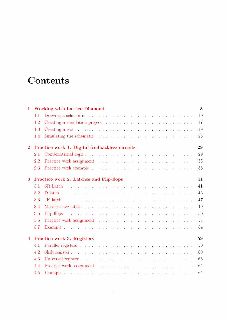
Contents
1 Working with Lattice Diamond 31.1 Drawing a schematic . . . . . . . . . . . . . . . . . . . . . . . . . . . . . . 101.2 Creating a simulation project . . . . . . . . . . . . . . . . . . . . . . . . . 171.3 Creating a test . . . . . . . . . . . . . . . . . . . . . . . . . . . . . . . . . 191.4 Simulating the schematic . . . . . . . . . . . . . . . . . . . . . . . . . . . . 25
2 Practice work 1. Digital feedbackless circuits 292.1 Combinational logic . . . . . . . . . . . . . . . . . . . . . . . . . . . . . . . 292.2 Practice work assignment . . . . . . . . . . . . . . . . . . . . . . . . . . . . 352.3 Practice work example . . . . . . . . . . . . . . . . . . . . . . . . . . . . . 36
3 Practice work 2. Latches and Flip-flops 413.1 SR Latch . . . . . . . . . . . . . . . . . . . . . . . . . . . . . . . . . . . . 413.2 D latch . . . . . . . . . . . . . . . . . . . . . . . . . . . . . . . . . . . . . . 463.3 JK latch . . . . . . . . . . . . . . . . . . . . . . . . . . . . . . . . . . . . . 473.4 Master-slave latch . . . . . . . . . . . . . . . . . . . . . . . . . . . . . . . . 493.5 Flip flops . . . . . . . . . . . . . . . . . . . . . . . . . . . . . . . . . . . . 503.6 Practice work assignment . . . . . . . . . . . . . . . . . . . . . . . . . . . . 533.7 Example . . . . . . . . . . . . . . . . . . . . . . . . . . . . . . . . . . . . . 54
4 Practice work 3. Registers 594.1 Parallel registers . . . . . . . . . . . . . . . . . . . . . . . . . . . . . . . . 594.2 Shift register . . . . . . . . . . . . . . . . . . . . . . . . . . . . . . . . . . . 604.3 Universal register . . . . . . . . . . . . . . . . . . . . . . . . . . . . . . . . 634.4 Practice work assignment . . . . . . . . . . . . . . . . . . . . . . . . . . . . 644.5 Example . . . . . . . . . . . . . . . . . . . . . . . . . . . . . . . . . . . . . 64
1

Contents 2
A Assignment tasks 68A.1 Tasks for practice work 1 . . . . . . . . . . . . . . . . . . . . . . . . . . . . 68A.2 Tasks for practice work 2 . . . . . . . . . . . . . . . . . . . . . . . . . . . . 70A.3 Tasks for practice work 3 . . . . . . . . . . . . . . . . . . . . . . . . . . . . 72

Chapter 1
Working with Lattice Diamond
Lattice Diamond design software uses projects for navigation. A project is comprisedof files schematically or logically describing the design, hardware types and sources. Allfiles are stored in a single folder. To create a project folder:
• Create an empty folder, name it after the work it contains i.e: lab1.
• Launch Lattice Diamond.
After the system starts, a Start Page is displayed. It is shown in 1.1.
Figure 1.1: ’Lattice Diamond’ start page
3

4
In the Start Page’s Project tab, select New. A new project window is opened. Bypressing the Next button open a project naming window. It is displayed in 1.2.
Figure 1.2: Project naming window
Give the new project a name by typing it in the window’s Name field (it is namedDemo in this exercise). Press the Next button. the Additional Sources window shouldbe left blank. We will not use additional sources in this exercise. After pressing the Nextbutton, a Device Selection window, shown in 1.3 is displayed.

5
Figure 1.3: Device selection window
Selections need to be made in the corresponding fields:
• Family - MachXO02,
• Device - LCMXO2-1200ZE,
• Package type - CSBGA132,
• Operating conditions - Commercial.
Press the Next button. In the Synthesis Tool selection window select SnynplifyPro from the list. An information window shown in 1.4 appears.

6
Figure 1.4: Project information window
Press the Finish button. A project summary window, shown in 1.5 will apear.
Figure 1.5: Project summary window

7
In the File List tab, right-click the project name. A pop-up window, shown in 1.6 willappear.
Figure 1.6: Pop-up window
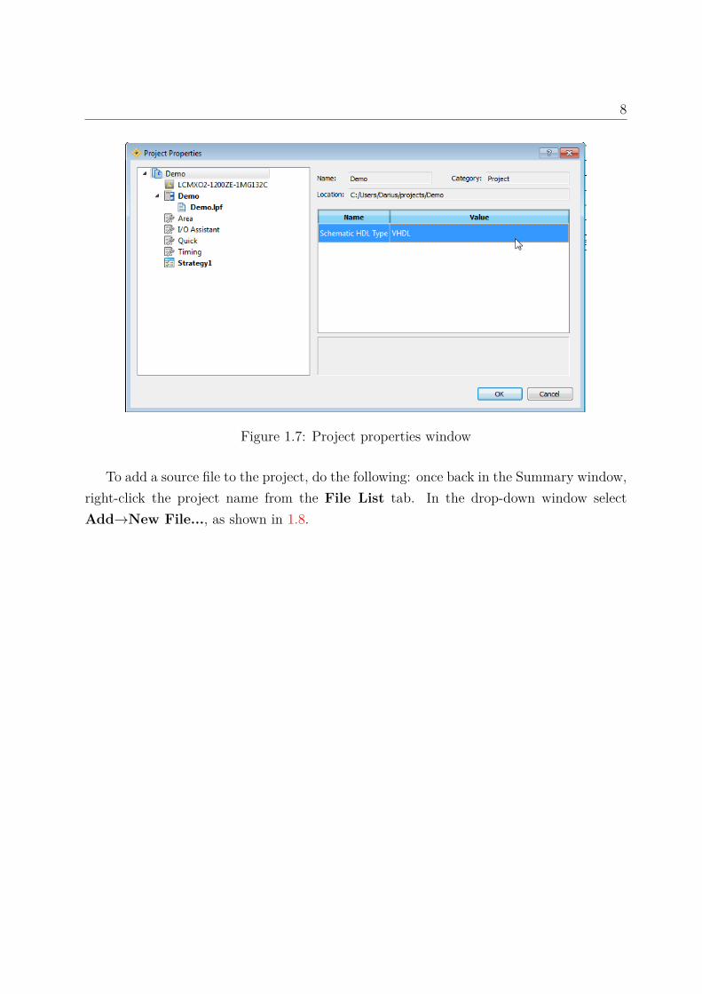
Choose Properties in the pop-up window. In this window, shown in 1.7, the Valuefield is set to Verilog. This book uses VHDL (Very High Speed Intergrated Circuit Descrip-tion Language) as the main language for describing digital logic. Therefore the Value fieldhas to be changed to VHDL. Click Verilog and select VHDL. Press the OK button.
8
Figure 1.7: Project properties window
To add a source file to the project, do the following: once back in the Summary window,right-click the project name from the File List tab. In the drop-down window selectAdd→New File..., as shown in 1.8.

9
Figure 1.8: Adding a new file to a project
In the new file window, shown in 1.9 in the Source Files field, select Schematic Files.Type the name of the file in the Name field. The Location field shows the path to anewly created file. The Add to Implementation box has to be selected. Press the Newbutton (1.9).

1.1. Drawing a schematic 10
Figure 1.9: New file window
1.1 Drawing a schematic
Once a new schematic file is opened, a schematic designer is displayed in the mainproject window (1.10).

1.1. Drawing a schematic 11
Figure 1.10: Schematic designer window
The schematic designer displays a sheet for creating a circuit. If the sheet size is to smallor large, it can be changed in the main menu by selecting Edit→Sheet and choosing thedesired sheet size. The sheet is normally displayed with a grid. This helps with componentalignment. If it is not displayed, it can be turned on by selecting Tools→Options fromthe main menu, select Schematic Editor→Graphics→Show Grid.
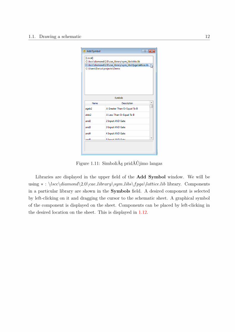
To begin drawing the circuit, first place the needed logic components on the sheet. Thisis done by right-clicking on the sheet. In the drop-down menu Add select Symbol (logiccomponents and other logical blocks are called symbols in this design software). A AddSymbol window, shown in 1.11 is opened.
1.1. Drawing a schematic 12
Figure 1.11: SimboliÅş pridÄŮjimo langas
Libraries are displayed in the upper field of the Add Symbol window. We will beusing ∗ : \lscc\diamond\2.0\cae library\sym libs\fpga\lattice.lib library. Componentsin a particular library are shown in the Symbols field. A desired component is selectedby left-clicking on it and dragging the cursor to the schematic sheet. A graphical symbolof the component is displayed on the sheet. Components can be placed by left-clicking inthe desired location on the sheet. This is displayed in 1.12.

1.1. Drawing a schematic 13
Figure 1.12: Placing logic components in the schematic
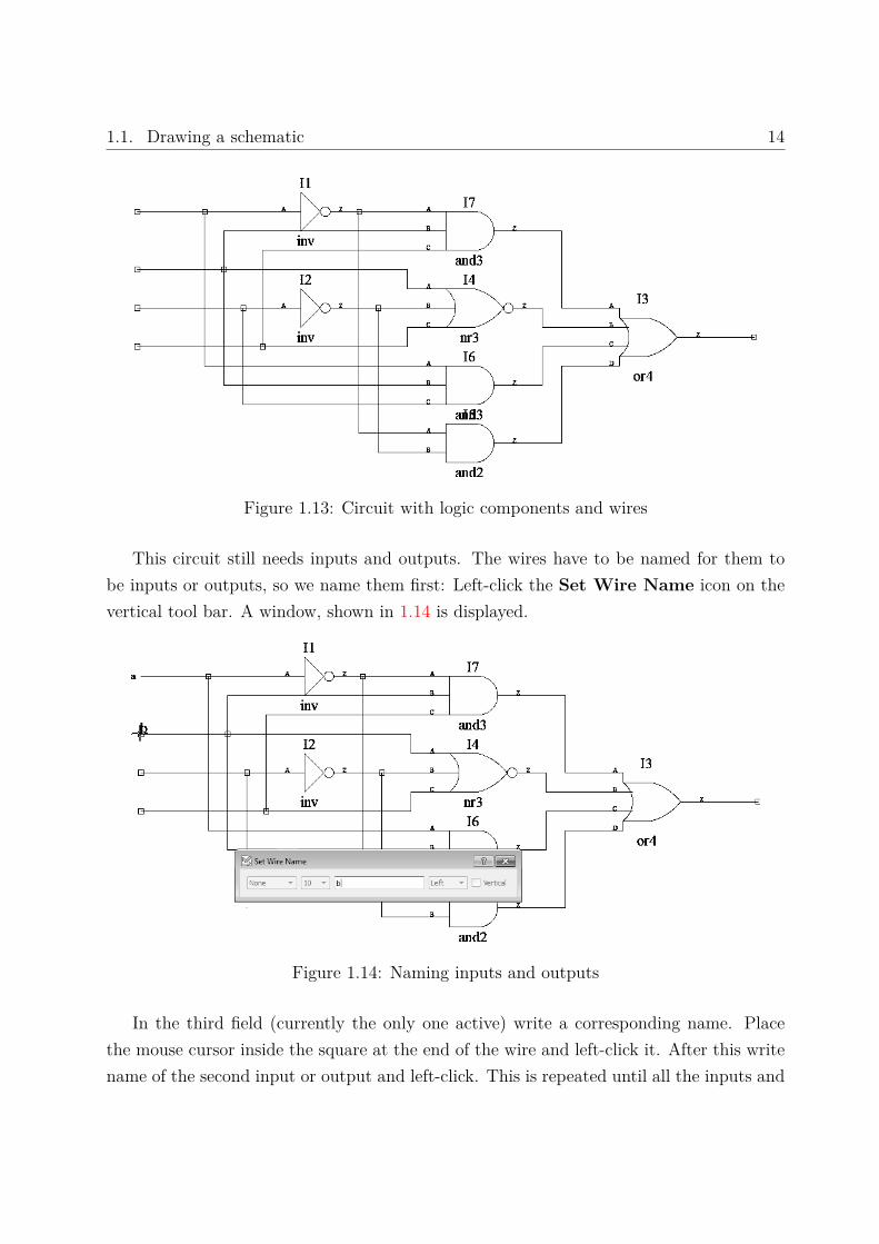
In 1.12 components are placed horizontally and vertically. All components are posi-tioned horizontally by default. To rotate a component press Ctrl+R on the keyboard,before placing the component on the sheet. We then connect the inputs and outputs of thecomponents. To do this, right-click on empty space in the sheet and select Add→Wire.All aforementioned actions can be accomplished by using a vertical toolbar in the schematicdesign window i.e. a wire can be added by pressing the fourth button from the top (Wire).To draw a wire, place the cursor on the spot where the wire should begin, left-click the spotand , holding the button, place the cursor on the spot where the wire ends. Release the leftmouse button. Only vertical and horizontal wire placement is allowed. If the signals areconnected, the connection is displayed by a small square. If the square does not appear,the signals are not connected. This should be noted to avoid errors in the circuit. Thewired circuit is displayed in 1.13.
1.1. Drawing a schematic 14
Figure 1.13: Circuit with logic components and wires
This circuit still needs inputs and outputs. The wires have to be named for them tobe inputs or outputs, so we name them first: Left-click the Set Wire Name icon on thevertical tool bar. A window, shown in 1.14 is displayed.
Figure 1.14: Naming inputs and outputs
In the third field (currently the only one active) write a corresponding name. Placethe mouse cursor inside the square at the end of the wire and left-click it. After this writename of the second input or output and left-click. This is repeated until all the inputs and

1.1. Drawing a schematic 15
outputs of the schematic are named. The direction of the pins (input or output) needs tobe set. To do this press the Set IO Type button on the vertical toolbar, as shown in 1.15.A window is displayed. Select the first drop down list and select Input in the first field ofthe window.
Figure 1.15: Selecting inputs in the schematic
Select the inputs in the schematic by dragging the box around them. One or all of theinputs can be selected at once. In 1.15 all four inputs are selected. Once the left mousebutton is released, wires a, b, c and d are set to inputs. This is repeated, until all inputsare set. The outputs are set in the same manner, by selecting Output in the Set IO Typewindow and selecting all the outputs.

1.1. Drawing a schematic 16
Figure 1.16: Selecting outputs in the schematic
The completed circuit is shown in 1.17.
Figure 1.17: Complete schematic
The created schematic needs to be saved. Select File→Save from the main menu.After saving, select the Process bar at the left. This is shown in 1.18.
1.2. Creating a simulation project 17
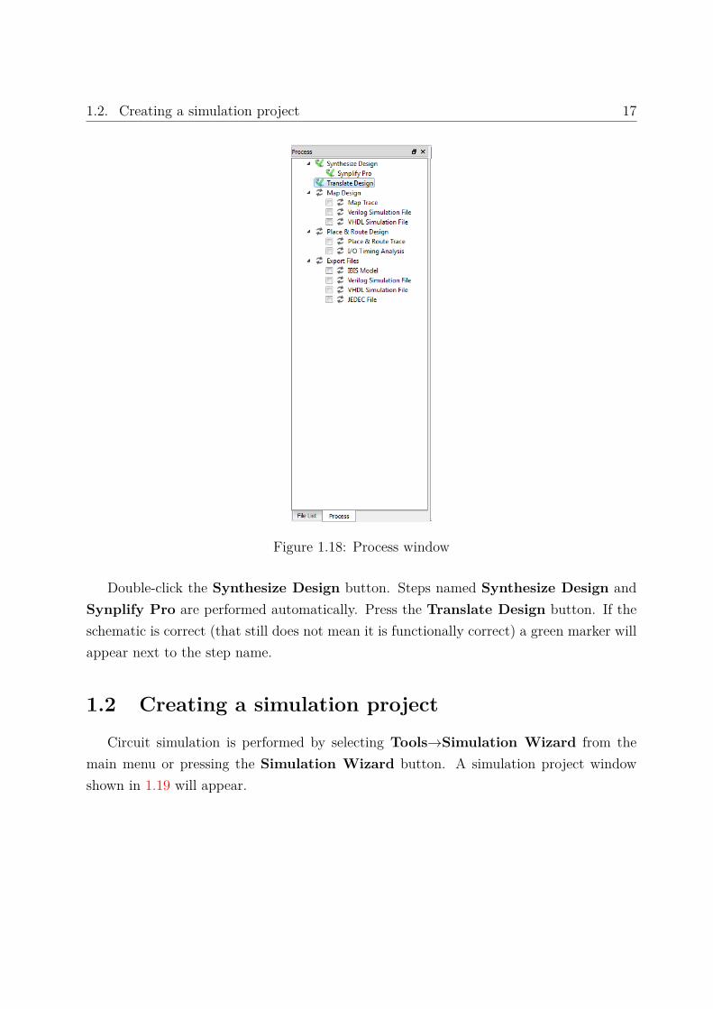
Figure 1.18: Process window
Double-click the Synthesize Design button. Steps named Synthesize Design andSynplify Pro are performed automatically. Press the Translate Design button. If theschematic is correct (that still does not mean it is functionally correct) a green marker willappear next to the step name.
1.2 Creating a simulation project
Circuit simulation is performed by selecting Tools→Simulation Wizard from themain menu or pressing the Simulation Wizard button. A simulation project windowshown in 1.19 will appear.

1.2. Creating a simulation project 18
Figure 1.19: Simulation project naming window
In the Project name field write a name for the simulation project. If the RTLselection in the Process Stage field is greyed-out, the Translate Design step was notperformed or was completed with errors. If that is the case, errors need to be correctedand the aforementioned steps repeated. When the Simulation Whizard guide finishes asimulation window, shown in 1.20 is displayed.
1.3. Creating a test 19
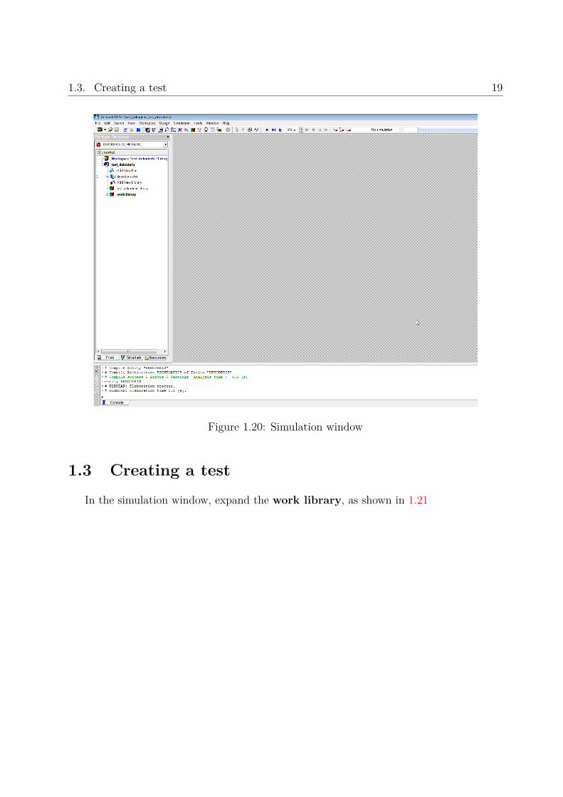
Figure 1.20: Simulation window
1.3 Creating a test
In the simulation window, expand the work library, as shown in 1.21

1.3. Creating a test 20
Figure 1.21: Test generation
Right click the schematic file and select the Generate TestBench option. A window,shown in 1.22 is displayed.

1.3. Creating a test 21
Figure 1.22: Device under test selection window
If the project contains more than one circuit, the Entity field needs to be set to thecircuit that is currently being simulated. If the project contains only one circuit, it isselected by default. The only thing to do is to check if it is correct. In the Architecturefield, select schematic. In the Testbench Type field, select Single Process. Other fieldsdo not require changes. Press the Finish button to complete the guide. A test creationwindow will appear.

1.3. Creating a test 22
Figure 1.23: Test creation window
The VHDL test code is presented below. In it, the schematic is connected to thesimulation environment. To perform the simulation, a test in VHDL, containing testvectors, witch describe the inputs at every given time needs to be created. The code givenbelow has to be copied to the file after the lines âĂđ– Add your stimulus hereâĂIJ. Testvectors are described in VHDL language. By using the assignment <= operator inputsreceive logic values. They can be ’0’ for logic low and ’1’ for logic high. The wait commandsets the time for value change.library ieee;

1.3. Creating a test 23
use ieee. std_logic_1164 .all;library machxo2 ;use machxo2 . components .all;
-- Add your library and packages declaration here ...
entity pav_tb isend pav_tb ;
architecture TB_ARCHITECTURE of pav_tb is-- Component declaration of the tested unitcomponent pavport(
a : in STD_LOGIC ;c : in STD_LOGIC ;d : in STD_LOGIC ;f : out STD_LOGIC ;b : in STD_LOGIC );
end component ;
-- Stimulus signals - signals mapped to-- the input and inout ports of tested entitysignal a : STD_LOGIC ;signal c : STD_LOGIC ;signal d : STD_LOGIC ;signal b : STD_LOGIC ;-- Observed signals - signals mapped to-- the output ports of tested entitysignal f : STD_LOGIC ;
-- Add your code here ...
begin
-- Unit Under Test port mapUUT : pav
port map (a => a,c => c,d => d,f => f,b => b
);
-- Add your stimulus here ...process begin
a <= '0'; b <= '0'; c <= '0'; d <= '0';wait for 10 ns;a <= '0'; b <= '0'; c <= '0'; d <= '1';wait for 10 ns;a <= '0'; b <= '0'; c <= '1'; d <= '0';
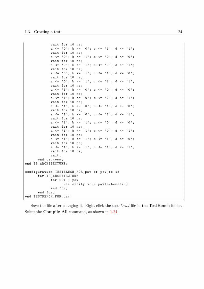
1.3. Creating a test 24
wait for 10 ns;a <= '0'; b <= '0'; c <= '1'; d <= '1';wait for 10 ns;a <= '0'; b <= '1'; c <= '0'; d <= '0';wait for 10 ns;a <= '0'; b <= '1'; c <= '0'; d <= '1';wait for 10 ns;a <= '0'; b <= '1'; c <= '1'; d <= '0';wait for 10 ns;a <= '0'; b <= '1'; c <= '1'; d <= '1';wait for 10 ns;a <= '1'; b <= '0'; c <= '0'; d <= '0';wait for 10 ns;a <= '1'; b <= '0'; c <= '0'; d <= '1';wait for 10 ns;a <= '1'; b <= '0'; c <= '1'; d <= '0';wait for 10 ns;a <= '1'; b <= '0'; c <= '1'; d <= '1';wait for 10 ns;a <= '1'; b <= '1'; c <= '0'; d <= '0';wait for 10 ns;a <= '1'; b <= '1'; c <= '0'; d <= '1';wait for 10 ns;a <= '1'; b <= '1'; c <= '1'; d <= '0';wait for 10 ns;a <= '1'; b <= '1'; c <= '1'; d <= '1';wait for 10 ns;wait;
end process ;end TB_ARCHITECTURE ;
configuration TESTBENCH_FOR_pav of pav_tb isfor TB_ARCHITECTURE
for UUT : pavuse entity work.pav( schematic );
end for;end for;
end TESTBENCH_FOR_pav ;
Save the file after changing it. Right click the test *.vhd file in the TestBench folder.Select the Compile All command, as shown in 1.24

1.4. Simulating the schematic 25
Figure 1.24: Test compilation window
If the file is correct, compiling proceeds with no error messages.
1.4 Simulating the schematic
After successful compilation, right-click the *.do file in the TestBench folder and selectthe Execute command, as shown in 1.25.

1.4. Simulating the schematic 26
Figure 1.25: Launching the simulation
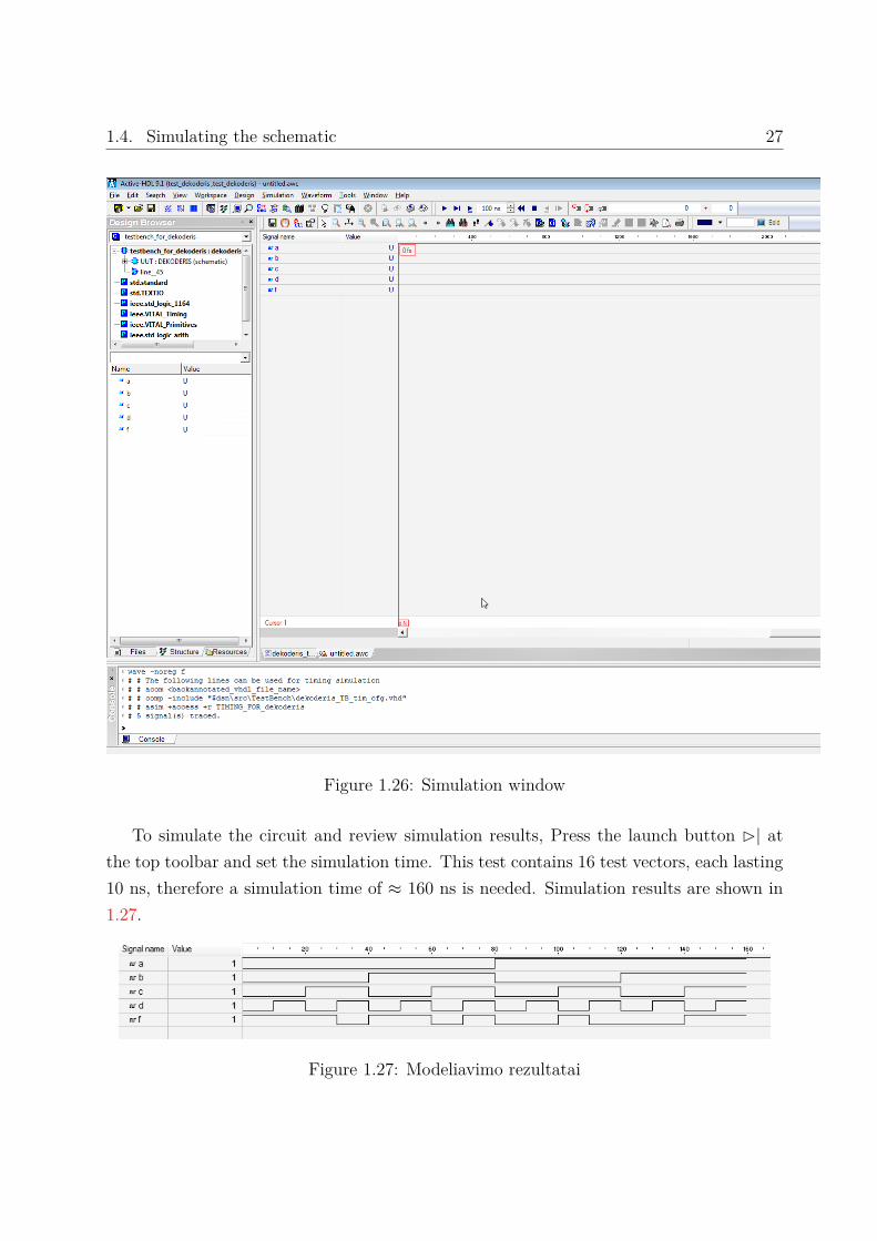
After execution a simulation window is displayed. It is shown in 1.26. If everythinguntil now is done correctly the simulation window contains inputs and outputs of the circuitbefore the test has begun.
1.4. Simulating the schematic 27
Figure 1.26: Simulation window
To simulate the circuit and review simulation results, Press the launch button B| atthe top toolbar and set the simulation time. This test contains 16 test vectors, each lasting10 ns, therefore a simulation time of ≈ 160 ns is needed. Simulation results are shown in1.27.
Figure 1.27: Modeliavimo rezultatai

1.4. Simulating the schematic 28
By using simulation results we conclude if the schematic is performing the desired function.
Chapter 2
Practice work 1. Digital feedbacklesscircuits
2.1 Combinational logic
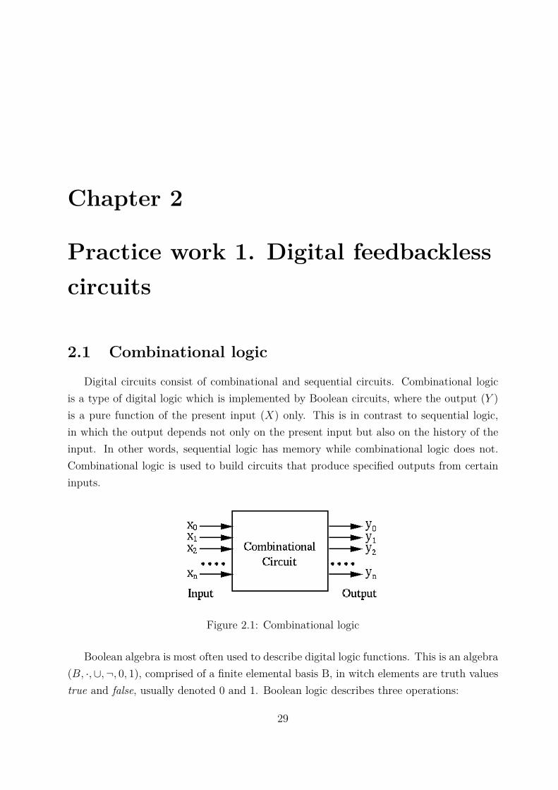
Digital circuits consist of combinational and sequential circuits. Combinational logicis a type of digital logic which is implemented by Boolean circuits, where the output (Y )is a pure function of the present input (X) only. This is in contrast to sequential logic,in which the output depends not only on the present input but also on the history of theinput. In other words, sequential logic has memory while combinational logic does not.Combinational logic is used to build circuits that produce specified outputs from certaininputs.
Figure 2.1: Combinational logic
Boolean algebra is most often used to describe digital logic functions. This is an algebra(B, ·,∪,¬, 0, 1), comprised of a finite elemental basis B, in witch elements are truth valuestrue and false, usually denoted 0 and 1. Boolean logic describes three operations:
29
2.1. Combinational logic 30
• AND operation (conjunction) ·,
• OR operation (disjunction) ∪,
• NOT operation (negation or inversion) ¬.
Each logic circuit realizes a Boolean function (output y value), arguments of witch areboolean variables (input x values). Boolean functions can be described as:
• truth tables, where a boolean function with n variables is described with all possible2n combinations of these variables;
• analytical notations, where a function is described with a formula;
• canonical forms, where a function is described as a sum of minterms or a product ofmaxterms.
• Karnaugh (Veitch) maps, where the function is described graphically.
Example
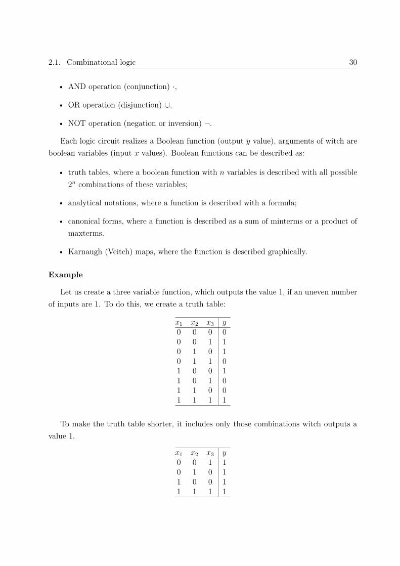
Let us create a three variable function, which outputs the value 1, if an uneven numberof inputs are 1. To do this, we create a truth table:
x1 x2 x3 y0 0 0 00 0 1 10 1 0 10 1 1 01 0 0 11 0 1 01 1 0 01 1 1 1
To make the truth table shorter, it includes only those combinations witch outputs avalue 1.
x1 x2 x3 y0 0 1 10 1 0 11 0 0 11 1 1 1

2.1. Combinational logic 31
Let us write down the sum of minterms for this particular function:
f = x1 · x2 · x3 ∪ x1 · x2 · x3 ∪ x1x2 · x3 ∪ x1 · x2 · x3 . (2.1)
By finding the common variables, this function can be rewritten as:
f = x1(x2 · x3 ∪ x2 · x3) ∪ x1(x2 · x3 ∪ x2 · x3) . (2.2)
or, by using the laws of boolean algebra we can rewrite the equation as:
f = x1(x2 ⊕ x3) ∪ x1(x2 ⊕ x3) = x1 ⊕ x2 ⊕ x3 . (2.3)
Let us write the functions disjunctive normal form (numbers, corresponding to thetruth table):
f = (1, 2, 4, 7) . (2.4)
The boolean functions can have many different forms. The function is often simplified,so that it can be implemented using a minimum number of physical logic gates. Karnaughmaps are often used for this task. The required boolean results are transferred from a truthtable onto a two-dimensional grid where the cells are ordered in Gray code, and each cellposition represents one combination of input conditions, while each cell value representsthe corresponding output value. Optimal groups of 1s or 0s are identified, which representthe terms of a canonical form of the logic in the original truth table. These terms can beused to write a minimal boolean expression representing the required logic. The Karnaughmap for function 2.4 is presented in 2.1:
Table 2.1: Karnaugh map for (2.4) functionx3 0 1
x1x200 101 111 110 1
Combinational logic circuits are comprised of logic gates. They are designed in thefollowing order:
1. Logic functions and functions’ arguments are found.
2.1. Combinational logic 32
2. A logic function is created, witch the designed circuit must produce. This functioncan be presented as a truth table or normal form.
3. The function is minimised, using commonly used methods (Karnaugh maps, Kwainand Mclasky), to achieve a minimal form. This form can be further rearranged, asto simplify logic gate design.
4. Synthesis is performed: the function is implemented using logic gates. A combina-tional logic schematic is created. To do this automatic synthesis methods can beused, as to meet the size, speed and power constraints.
5. After synthesis, a test is created. It is a sequence of inputs, that tests if the schematicis working in the desired way.
Example
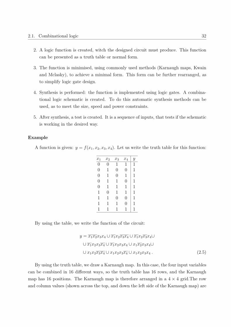
A function is given: y = f(x1, x2, x3, x4). Let us write the truth table for this function:
x1 x2 x3 x4 y0 0 1 1 10 1 0 0 10 1 0 1 10 1 1 0 10 1 1 1 11 0 1 1 11 1 0 0 11 1 1 0 11 1 1 1 1
By using the table, we write the function of the circuit:
y = x1x2x3x4 ∪ x1x2x3x4 ∪ x1x2x3x4∪
∪ x1x2x3x4 ∪ x1x2x3x4 ∪ x1x2x3x4∪
∪ x1x2x3x4 ∪ x1x2x3x4 ∪ x1x2x3x4 . (2.5)
By using the truth table, we draw a Karnaugh map. In this case, the four input variablescan be combined in 16 different ways, so the truth table has 16 rows, and the Karnaughmap has 16 positions. The Karnaugh map is therefore arranged in a 4 × 4 grid.The rowand column values (shown across the top, and down the left side of the Karnaugh map) are

2.1. Combinational logic 33
ordered in Gray code rather than binary numerical order. Gray code ensures that only onevariable changes between each pair of adjacent cells. Each cell of the completed Karnaughmap contains a binary digit representing the function’s output for that combination ofinputs. After the Karnaugh map has been constructed it is used to find one of the simplestpossible forms-a canonical form-for the information in the truth table. Adjacent 1s in theKarnaugh map represent opportunities to simplify the expression. The minterms for thefinal expression are found by encircling groups of 1s in the map. Minterm groups mustbe rectangular and must have an area that is a power of two (i.e. 1, 2, 4, 8...). Mintermrectangles should be as large as possible without containing any 0s. Groups may overlapin order to make each one larger. The optimal groupings in this example are markedby different colors. The red green and blue groups overlap. The red group is a 4 × 1rectangle, the blue group 1 × 4 rectangle. The grid is toroidally connected, which meansthat rectangular groups can wrap across the edges. Cells on the extreme right are actually’adjacent’ to those on the far left; similarly, so are those at the very top and those at thebottom. Therefore the green group - a 2× 2 square is valid.
x3x4 00 01 11 10x1x200 101 1 1 1 111 1 1 110 1
Once the Karnaugh map has been constructed and the adjacent 1s linked by rectangularand square boxes, the algebraic minterms can be found by examining which variables staythe same within each box.
In the green group:
• Variable x1 does not maintain the same state (it shifts from 0 to 1), and shouldtherefore be excluded.
• Variable x2 is the same and is equal to 1 throughout the box, therefore it should beincluded in the algebraic representation of the minterm.
• Variable x3 does not maintain the same state and is therefore excluded.
• Variable x4 does not change. It is always 0 so its complement, NOT − x4, should beincluded thus, x4.
2.1. Combinational logic 34
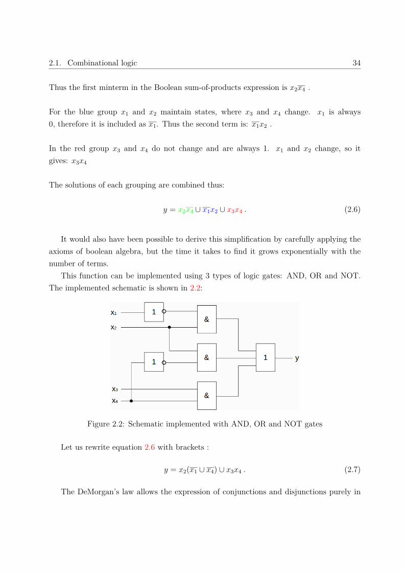
Thus the first minterm in the Boolean sum-of-products expression is x2x4 .
For the blue group x1 and x2 maintain states, where x3 and x4 change. x1 is always0, therefore it is included as x1. Thus the second term is: x1x2 .
In the red group x3 and x4 do not change and are always 1. x1 and x2 change, so itgives: x3x4
The solutions of each grouping are combined thus:
y = x2x4 ∪ x1x2 ∪ x3x4 . (2.6)
It would also have been possible to derive this simplification by carefully applying theaxioms of boolean algebra, but the time it takes to find it grows exponentially with thenumber of terms.
This function can be implemented using 3 types of logic gates: AND, OR and NOT.The implemented schematic is shown in 2.2:
Figure 2.2: Schematic implemented with AND, OR and NOT gates
Let us rewrite equation 2.6 with brackets :
y = x2(x1 ∪ x4) ∪ x3x4 . (2.7)
The DeMorgan’s law allows the expression of conjunctions and disjunctions purely in

2.2. Practice work assignment 35
terms of each other via negation. The law can be written as:
a ∪ b = a · b . (2.8)
By using DeMorgan’s law on the 2.7 equation, we get:
y = x2 · x1x4 · x3x4 . (2.9)
This function can be implemented by using NAND (NOT-AND) gates. A schematicusing only NAND gates is shown in 2.3:
Figure 2.3: Schematic implemented using NAND gates
The schematic shown in 2.2 is designed with 3 types of different components, while theschematic in 2.3 needs only one type of component.
2.2 Practice work assignment
In the assignment table (A.1), Each student gets his task according to their number inthe group. Functions, with their minterms are given. To complete the assignment:
1. Write the given function in sum-of-minterms form.
2. Minimize the given function
3. Implement the given function in 3 different ways:
• using AND, OR, NOT gates,

2.3. Practice work example 36
• using only NAND, NOR and NOT gates,
• using a multiplexer.
4. Test the functionality of created schematics;
5. Present a summary in written form. The summary should contain equations, schemat-ics, test results and conclusions.
2.3 Practice work example
The given function is:
f = 1, 2, 3, 9, 17, 20, 21, 22, 23, 25, 33, 41, 49, 57, 61, 63 (2.10)
We write this function down in disjunctive normal form. Every number is a minterm.
f = x1x2x3x4x5x6 ∪ x1x2x3x4x5x6 ∪ x1x2x3x4x5x6 ∪ x1x2x3x4x5x6∪
∪ x1x2x3x4x5x6 ∪ x1x2x3x4x5x6 ∪ x1x2x3x4x5x6 ∪ x1x2x3x4x5x6∪ (2.11)∪ x1x2x3x4x5x6 ∪ x1x2x3x4x5x6 ∪ x1x2x3x4x5x6 ∪ x1x2x3x4x5x6∪
∪ x1x2x3x4x5x6 ∪ x1x2x3x4x5x6 ∪ x1x2x3x4x5x6 ∪ x1x2x3x4x5x6.
We then create a Karnaugh map and fill it with function values.
x4x5x6 000 001 011 010 110 111 101 100x1x2x3000 1 1 1001 1011 1010 1 1 1 1 1110 1111 1 1 1101 1100 1
With the help of a Karnaugh table the function is minimized (grouped minterms areshown in colors):

2.3. Practice work example 37
f = x1x2x3x4x5∪x4x5x6∪x1x2x3x4∪x1x2x3x4x6. (2.12)
We can further simplify the equation by finding common variables:
f = x1x2x3x4x5 ∪ x4x5x6 ∪ x1x2x3x4 ∪ x1x2x3x4x6 == x1x3(x2x4x5 ∪ x2x4) ∪ x6(x4x5 ∪ x1x2x3x4). (2.13)
The schematic for the given function is shown in 2.4
Figure 2.4: Implementation of the schematic with AND, OR and NOT gates
To implement the second schematic with NAND and NOR gates, we rearrange thefunction, so it looks like this:
f = x1x3(x2x4x5 ∪ x2x4) ∪ x6(x4x5 ∪ x1x2x3x4). (2.14)
By using DeMorgan’s law (a ∪ b = a · b) on the equation, we get the following:
2.3. Practice work example 38
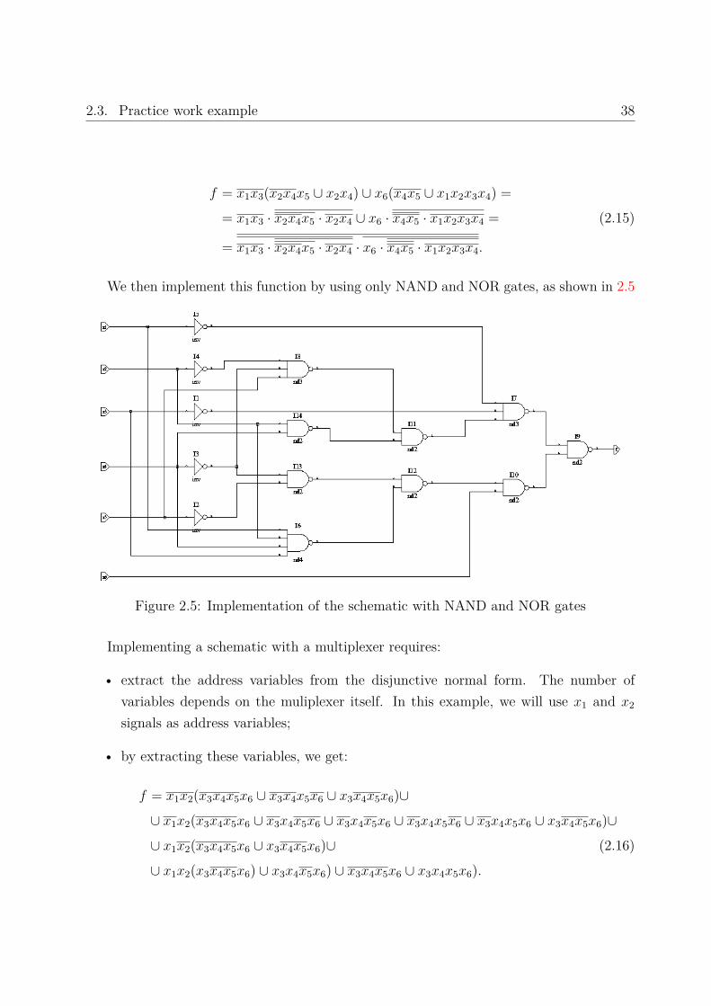
f = x1x3(x2x4x5 ∪ x2x4) ∪ x6(x4x5 ∪ x1x2x3x4) == x1x3 · x2x4x5 · x2x4 ∪ x6 · x4x5 · x1x2x3x4 = (2.15)
= x1x3 · x2x4x5 · x2x4 · x6 · x4x5 · x1x2x3x4.
We then implement this function by using only NAND and NOR gates, as shown in 2.5
Figure 2.5: Implementation of the schematic with NAND and NOR gates
Implementing a schematic with a multiplexer requires:
• extract the address variables from the disjunctive normal form. The number ofvariables depends on the muliplexer itself. In this example, we will use x1 and x2
signals as address variables;
• by extracting these variables, we get:
f = x1x2(x3x4x5x6 ∪ x3x4x5x6 ∪ x3x4x5x6)∪∪ x1x2(x3x4x5x6 ∪ x3x4x5x6 ∪ x3x4x5x6 ∪ x3x4x5x6 ∪ x3x4x5x6 ∪ x3x4x5x6)∪∪ x1x2(x3x4x5x6 ∪ x3x4x5x6)∪ (2.16)∪ x1x2(x3x4x5x6) ∪ x3x4x5x6) ∪ x3x4x5x6 ∪ x3x4x5x6).

2.3. Practice work example 39
The implementation of the function with a multiplexer is shown in 2.6
Figure 2.6: Funkcijos realizacija su mulitplekseriu
To create a test, we will use several processes in VHDL language. There is no constrainton process count in VHDL. They are created as needed. All processes run parallel (at thesame time). The process is endless - when the last assignment is executed the process isrestarted and executes from the beginning. The test is made to produce all possible inputcombinations. Therefore, 6 processes are used, controlling each input separately. The testis halted at the end, using a special assert command.
-- Add your stimulus here ...x6p: processbegin
x6 <= '0';wait for 10 ns;x6 <= '1';wait for 10 ns;
end process ;
x5p: processbegin
x5 <= '0';wait for 20 ns;x5 <= '1';wait for 20 ns;
end process ;

2.3. Practice work example 40
x4p: processbegin
x4 <= '0';wait for 40 ns;x4 <= '1';wait for 40 ns;
end process ;
x3p: processbegin
x3 <= '0';wait for 80 ns;x3 <= '1';wait for 80 ns;
end process ;
x2p: processbegin
x2 <= '0';wait for 160 ns;x2 <= '1';wait for 160 ns;
end process ;
x1p: processbegin
x1 <= '0';wait for 320 ns;x1 <= '1';wait for 320 ns;assert false report "End of test" severity failure ;
end process ;
By using the example code in the *.vhd file we get time diagrams shown in 2.7.
Figure 2.7: Time diagrams of the schematic
We note that when inputs receive one of the values in the exercise, the output f is changedto logic high (1). In other cases the output is logic low (0). By using the test, we concludethat all three schematics are working properly.
Chapter 3
Practice work 2. Latches andFlip-flops
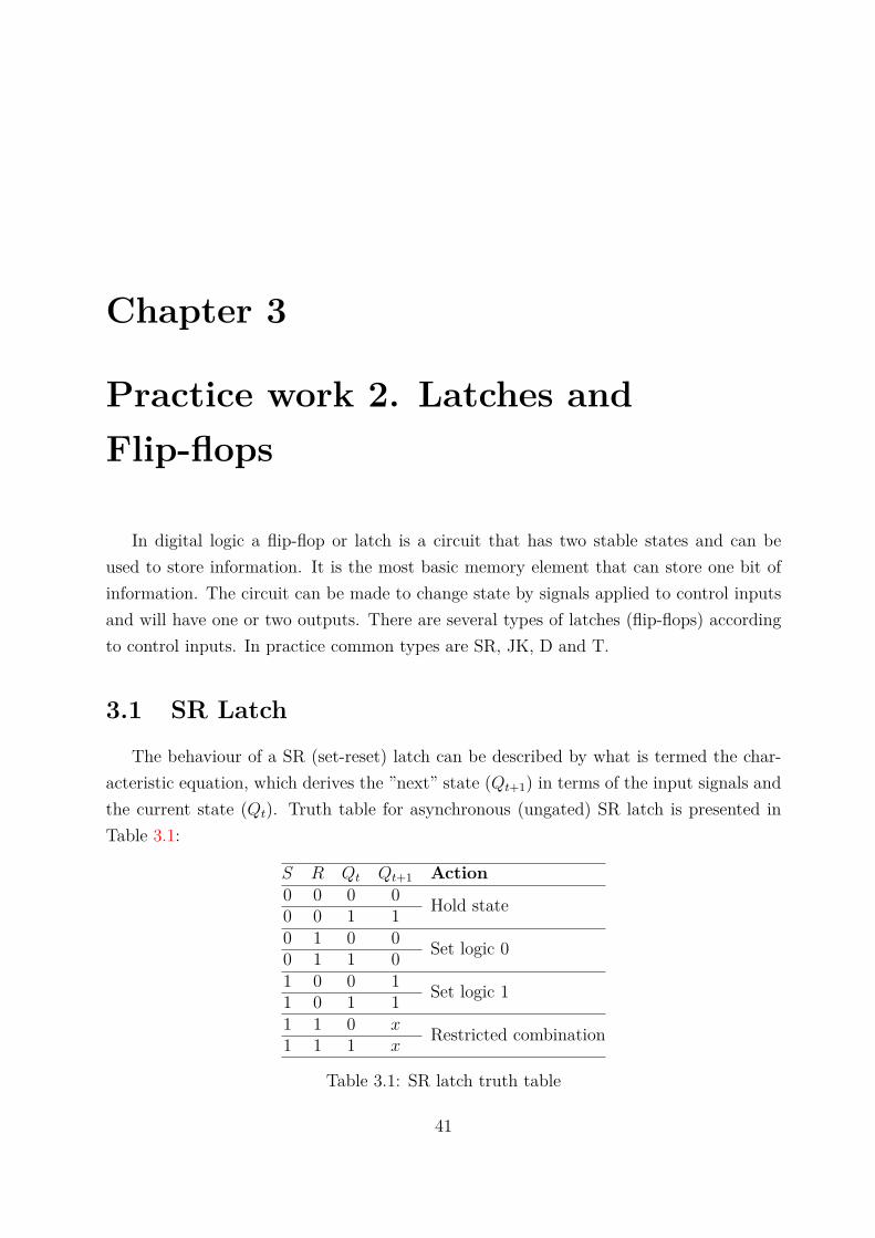
In digital logic a flip-flop or latch is a circuit that has two stable states and can beused to store information. It is the most basic memory element that can store one bit ofinformation. The circuit can be made to change state by signals applied to control inputsand will have one or two outputs. There are several types of latches (flip-flops) accordingto control inputs. In practice common types are SR, JK, D and T.
3.1 SR Latch
The behaviour of a SR (set-reset) latch can be described by what is termed the char-acteristic equation, which derives the ”next” state (Qt+1) in terms of the input signals andthe current state (Qt). Truth table for asynchronous (ungated) SR latch is presented inTable 3.1:
S R Qt Qt+1 Action0 0 0 0 Hold state0 0 1 10 1 0 0 Set logic 00 1 1 01 0 0 1 Set logic 11 0 1 11 1 0 x Restricted combination1 1 1 x
Table 3.1: SR latch truth table
41

3.1. SR Latch 42
The stored bit is present on the output marked Q. The marking Qt represents thecurrent state of the latch and Qt+1) represent the state after inputs change. Usuallylatches and flip-flops have output Q which display an inverse of the current state. An SRlatch has two inputs - S (stand for Set) and R (stand for Reset). Using Table 3.1 we canwrite a characteristic equation of SR latch:
Qt+1 = SRQt ∪ SRQt ∪ SRQt = R(Qt ∪ S). (3.1)
This equation can be implemented using only NAND gates. To do so we apply DeMor-gan’s Law:
Qt+1 = R(Qt ∪ S) = R ·Q · S (3.2)
The schematic of SR NAND latch is shown in Figure 3.1 a).
Figure 3.1: Schematic of SR NAND latch a), symbol b), timing diagram c)
SR latches can be implemented using NOR gates. In this case the characteristic equa-tion is:
Qt+1 = R(Qt ∪ S) = R ∪ (Q ∪ S) (3.3)
The schematic of SR NOR latch is shown in Figure 3.2 a).

3.1. SR Latch 43
Figure 3.2: Schematic of SR NOR latch a), symbol b), timing diagram c)
Latches are designed to be transparent. That is, input signal changes cause immediatechanges in output; when several transparent latches follow each other, using the sameenable signal, signals can propagate through all of them at once. These latches are calledasynchronous. Alternatively, additional logic can be added to a transparent latch to makeit non-transparent or gated (synchronous).
According to the way of synchronization, memory elements can be divided in to basicgroups:
• Gated latches are level-sensitive elements. With synchronization signal C high(enable true), the signals can pass through the input gates to the encapsulated latch.With C low (enable false) the latch is closed and remains in the state it was left thelast time C was high.
• Master-Slave latches consist of two latches connected together. When signal C ishigh, the first latch is set, but the second latch does not change state. When signal C
is low, the first latch’s output is stored in the second latch, but the first latch cannotchange state.
• Flip-flops are logic level transition (edge) sensitive elements. A Flip flop’s outputonly changes when the synchronization signal C (usually called clock signal) changesfrom logic 0 to logic 1 (positive edge triggered) or from logic 1 to logic 0 (negativeedge triggered).
3.1. SR Latch 44
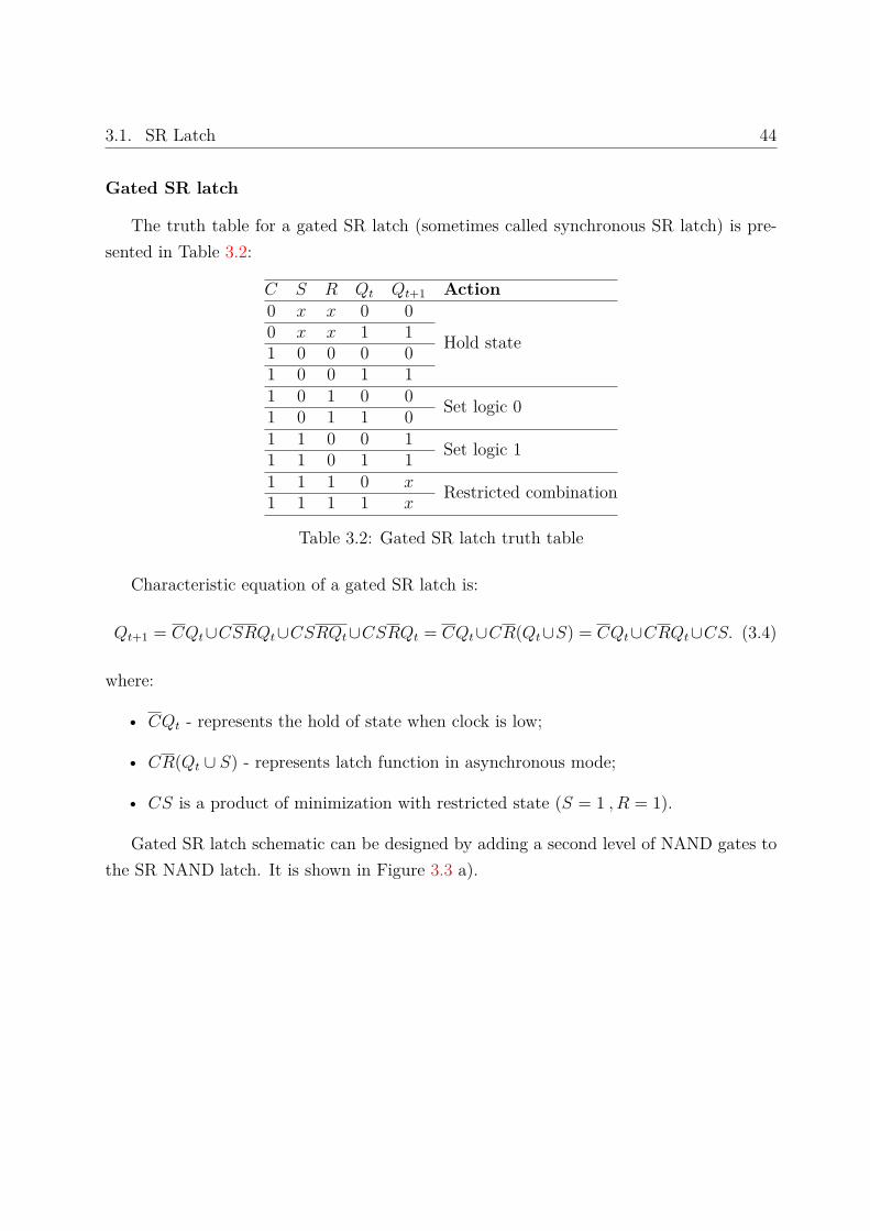
Gated SR latch
The truth table for a gated SR latch (sometimes called synchronous SR latch) is pre-sented in Table 3.2:
C S R Qt Qt+1 Action0 x x 0 0
Hold state0 x x 1 11 0 0 0 01 0 0 1 11 0 1 0 0 Set logic 01 0 1 1 01 1 0 0 1 Set logic 11 1 0 1 11 1 1 0 x Restricted combination1 1 1 1 x
Table 3.2: Gated SR latch truth table
Characteristic equation of a gated SR latch is:
Qt+1 = CQt∪CSRQt∪CSRQt∪CSRQt = CQt∪CR(Qt∪S) = CQt∪CRQt∪CS. (3.4)
where:
• CQt - represents the hold of state when clock is low;
• CR(Qt ∪ S) - represents latch function in asynchronous mode;
• CS is a product of minimization with restricted state (S = 1 , R = 1).
Gated SR latch schematic can be designed by adding a second level of NAND gates tothe SR NAND latch. It is shown in Figure 3.3 a).

3.1. SR Latch 45
Figure 3.3: Schematic of gated a SR latch a), symbol b) and timing diagram c)
To set the latch into an known initial state an additional signal is used. Usually thissignal is called Reset. It is used to change the state to logic 0. A schematic with Rst signalis shown in Figure 3.4.
Figure 3.4: Gated SR latch with Reset signal

3.2. D latch 46
3.2 D latch
D latches, as well as all other types of latches, are made from a simple SR latch. GatedD latches are made by connecting a complement of S (S) signal to input R as shown inFigure 3.5.
Figure 3.5: Gated D latch
This type of latch has one input - D (data) and a synchronization signal C (clock).When C = 1 signal propagates directly from the input D to the output Q. When C = 0a latch holds the state that was last set in active mode.
A truth table for D latch is presented in Table 3.3. Schematic, symbol and timingdiagrams are shown in Figure 3.6.
C D Qt Qt+1 Action0 x 0 0 Hold state0 x 1 11 0 0 0
Set output1 0 1 01 1 0 11 1 1 1
Table 3.3: Gated D latch truth table
Characteristic equation of a D type gated latch is:
Qt+1 = CQt ∪ CD. (3.5)
where CQt represents holding the current state and CD shows ”next” state’s dependencyon the D value, when C = 1.

3.3. JK latch 47
Figure 3.6: Schematic of a gated D latch a), symbol b) and timing diagram c)
3.3 JK latch
The JK latch augments the behaviour of the SR flip-flop (J=Set, K=Reset) by inter-preting the S = R = 1 condition as a toggle command. Truth table of the JK latch ispresented in Table 3.4.
J K Qt Qt+1 Action0 0 0 0 Hold state0 0 1 10 1 0 0 Set logic 00 1 1 01 0 0 1 Set logic 11 0 1 11 1 0 1 toggle state1 1 1 0
Table 3.4: Truth table of a JK latch

3.3. JK latch 48
Characteristic equation of a JK latch is:
Qt+1 = KQt ∪ JQt. (3.6)
Characteristic equation of gated JK latch can be made by inserting a clock C signal:
Qt+1 = CQt ∪ C(KQt ∪ JQt). (3.7)
Schematic is designed using simple SR latch that includes feedback from Q and Q
outputs to enabling NAND gates. It is displayed in Figure 3.7. Delay of the feedbacksignal is denoted tv.
Figure 3.7: Schematic of a gated JK latch a), symbol b) and timing diagrams c)
A T latch can be built using a JK latch. Connected J and K inputs act as input T
(shown in Figure 3.8. If the T input is high, the T latch changes state (”toggles”), if theT input is low, the latch holds the previous value.

3.4. Master-slave latch 49
Figure 3.8: Schematic of gated T latch a), symbol b) and timing diagram c)
3.4 Master-slave latch
A masterâĂŞslave latch is created by connecting two gated SR latches in series, andinverting the synchronization (clock) signal to one of them, as shown in Figure 3.9. Thename masterâĂŞslave comes from the second latch (slave) being responsive from the changein the first (master) latch. This type is often called MS latch.

3.5. Flip flops 50
Figure 3.9: Schematic of a master-slave JK latch a), symbol b) and timing diagram c)
When clock signal is high C = 1 master latch is set by input signals and slave latch is”locked”. As the clock signal goes low (1 to 0) the input to the master latch is ”locked”,nearly simultaneously these values are captured by slave latch.
3.5 Flip flops
The word latch is mainly used for level-sensitive memory elements, whereas a flip-flopis edge-sensitive. That is, when a latch is enabled it becomes transparent, while a flip flop’soutput only changes when clock goes form 0 to 1 (positive-edge) or from 1 to 0 (negativeedge). A schematic of SR flip flop is shown in Figure 3.10.

3.5. Flip flops 51
Figure 3.10: Schematic of SR flip flop a) and symbol b)
Gates E5 ir E6 form the main (output) latch, while gates E1 and E2 together with E3and E4 are secondary latches. Timing diagram of this schematic is shown in Figure 3.11.
Figure 3.11: Timing diagram of SR flip flop

3.5. Flip flops 52
In practice D flip flops are more common, due to there stability and simpler use.Schematic of D flip flop is shown in Figure 3.12.
Figure 3.12: Schematic of D flip flop, with set (S) and reset (R) inputs
In this schematic asynchronous inputs R are S are used set flip flop’s initial state (eitherlogic 0 or 1).
JK flip flops are also common (for example, 74ALS109 chip). Schematic is shown inFigure 3.13.

3.6. Practice work assignment 53
Figure 3.13: Schematic of JK flip flop
Other types of flip flops are also possible.
3.6 Practice work assignment
1. Design a gated latch. The type of latch is specified in the practice work assignment(A.2). Analyze it’s functionality.
2. Design a master-slave gated latch of the type specified in the practice work assignment(A.2). Analyze it’s functionality.
3. Design a flip flop of the type specified in the practice work assignment (A.2). Analyzeit’s functionality.
4. By using the gated latch or flip-flop from the previous assignment, connect theschematic, described in fig. 3.14.
5. Prepare a practice work report.

3.7. Example 54
Figure 3.14: Structure of the schematic to be analyzed
3.7 Example
An assignment is given:
• Type of schematic: SR
• master-slave latch;
• schematic 3.14a;
• synchronization signals C1, C2.
We start by designing a SR gated latch with a reset input, witch resets the latch to aknown state (’0’). The schematic is shown in 3.15.
Figure 3.15: Schematic of an SR gated latch

3.7. Example 55
The functionality of the latch is described by the SR latch truth table:
R S Qt+1 Action0 0 Qt Hold state1 0 0 Set logic 01 1 x Restricted0 1 1 Set logic 1
Table 3.5: SR trigerio teisingumo lentelÄŮ
By using the table we design a test for the gated latch. An example of the test ispresented in tab. ??. The test must fully test the functionality of the circuit.
We shall use 2 processes for testing the schematic- one for clock generation, the second- control signal generationprocess begin
C <= '0';wait for 8 ns;C <= '1';wait for 8 ns;
end process ;
process beginrst <= '0';S <= '0'; R <= '0';wait for 10 ns;rst <= '1';S <= '0'; R <= '0';wait for 10 ns;S <= '1'; R <= '0';wait for 10 ns;S <= '0'; R <= '0';wait for 30 ns;S <= '0'; R <= '1';wait for 10 ns;S <= '0'; R <= '0';wait for 30 ns;S <= '1'; R <= '0';wait for 10 ns;S <= '0'; R <= '0';wait for 30 ns;
end process ;
Since processes in VHDL language are endless, we must restrict the simulation time bypressing the Run Until B| or Run For B buttons and selecting the time needed for thetest to complete. After a simulation time of 200 ns, we get the timing diagrams:
3.7. Example 56
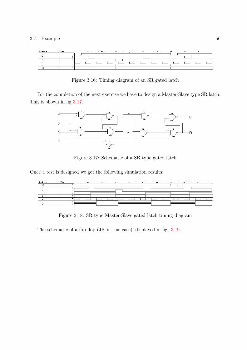
Figure 3.16: Timing diagram of an SR gated latch
For the completion of the next exercise we have to design a Master-Slave type SR latch.This is shown in fig 3.17.
Figure 3.17: Schematic of a SR type gated latch
Once a test is designed we get the following simulation results:
Figure 3.18: SR type Master-Slave gated latch timing diagram
The schematic of a flip-flop (JK in this case), displayed in fig. 3.19.

3.7. Example 57
Figure 3.19: JK type flip-flop schematic
The timing diagrams of the flip flop are presented in fig. 3.20 pav.
Figure 3.20: JK type flip-flop timing diagram
Compare the functions of the latch, master-slave latch and flip flop schematic. Makeappropriate conclusions afterward.
When designing the schematic shown in fig 3.14a, we shall use D type latches, created bymodifying SR type gated latches. Symbol generation is done by selecting Design→GenerateSymbol from the main menu. The C input of the latches are connected to a single source,according to the work assignment.
Figure 3.21: Schematic under test

3.7. Example 58
Figure 3.22: Timing diagrams of the schematic

Chapter 4
Practice work 3. Registers
In digital logic a register is a device that stores several bits of information. They are agroup of flip-flops connected together using some sort of control circuit. According to theway data is written and read to and out of the registers, they can be divided into severalgroups:
• Parallel registers;
• Shift registers;
• Universal registers.
Each bit stored in register has it index. In this book the least significant bit (LSB)has index 0 and is considered to be rightmost. It is due to the convention of writing lesssignificant bits further to the right.
4.1 Parallel registers
The transfer of new information into the register is referred to as loading the register.If all bits of the register are loaded simultaneously with a single clock pulse, we say thatthe loading is done in parallel. Parallel registers have n flip-flops, and control circuit forparallel data write and read. Since a flip flop can hold one bit of information, number n
defines register storage capacity.
59
4.2. Shift register 60
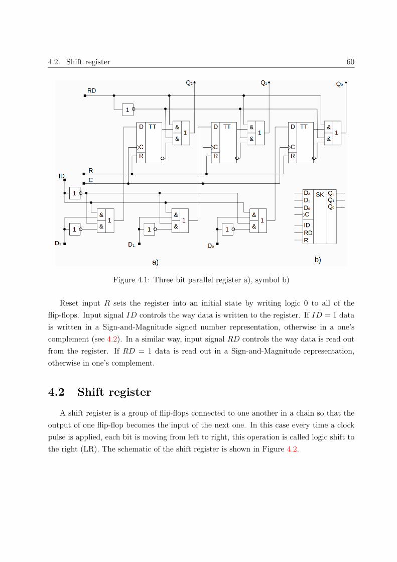
Figure 4.1: Three bit parallel register a), symbol b)
Reset input R sets the register into an initial state by writing logic 0 to all of theflip-flops. Input signal ID controls the way data is written to the register. If ID = 1 datais written in a Sign-and-Magnitude signed number representation, otherwise in a one’scomplement (see 4.2). In a similar way, input signal RD controls the way data is read outfrom the register. If RD = 1 data is read out in a Sign-and-Magnitude representation,otherwise in one’s complement.
4.2 Shift register
A shift register is a group of flip-flops connected to one another in a chain so that theoutput of one flip-flop becomes the input of the next one. In this case every time a clockpulse is applied, each bit is moving from left to right, this operation is called logic shift tothe right (LR). The schematic of the shift register is shown in Figure 4.2.

4.2. Shift register 61
Figure 4.2: 4 bit logic right shift register a), symbol b)
There are several types of shift operations:
1. Logic shift to the left or right (LL, LR). The vacant bit is filled with either a 0 or a1, depending on the outside input (DL or DR);
2. Circular shift to the left or right (CL, CR), all bits are shifted to either directionand the final bit is moved to the vacant flip-flop;
3. Arithmetic shift (AR, AL), for signed numbers, the most significant (sign) bit ispreserved and all other bits are shifted. The vacant bit is filled with either a 0 or a1, depending on the signed number’s representation.
Signed number representations
In computing, signed number representations are required to encode negative numbersin binary number systems. In mathematics, negative numbers are represented by prefixingthem with a ”-” sign. However, in digital logic, numbers are represented in bit vectorsonly, without extra symbols. Three best-known methods to represent signed numbers are:
1. Sign-and-magnitude;
2. Ones’ complement;
3. Two’s complement.
At present the most widely used representation is two’s complement.

4.2. Shift register 62
Sign-and-magnitude
In the first approach, the problem of representing a number’s sign can be to allocateone sign bit to represent the sign: set that bit (often the most significant bit) to logic 0for a positive number, and set to logic 1 for a negative number. Remaining bits in thenumber indicate the magnitude (or absolute value). In a byte only 7 bits represents themagnitude. It can range from 00000002 (010) to 11111112 (12710). Thus in a signed bytenumber for −12710 to +12710 can be represented.
A consequence of this representation is that there are two ways to represent zero,00000000 (0) and 10000000 (-0).
An example of sign-and-magnitude numbers:+26 : 00011010-26 : 10011010
Ones’ complement
The ones’ complement form of a negative binary number is the bit-wise NOT appliedto its positive counterpart. Like sign-and-magnitude representation, ones’ complement hastwo representations of zero: 000000002 (+010) and 111111112 (−010)..
An example of ones’ complement numbers:+26 : 00011010-26 : 11100101
Signed numbers in ones’ complement can range from −(2N−1 − 1) to +(2N−1 − 1) and±0. In previous expression N denotes number of bits.
Two’s complement
In two’s complement, negative numbers are represented by the bit pattern which isone greater (in an unsigned sense) than the ones’ complement of the positive value. Inthis representation there is only one zero, represented as 00000000. Negating a number(whether negative or positive) is done by inverting all the bits and then adding 1 to thatresult. Addition and subtraction of a pair of two’s-complement integers is the same asaddition of a pair of unsigned numbers. A method to get the negation of a number in two’scomplement is as follows:
1. Invert all the bits through the number,
2. Add 1;

4.3. Universal register 63
For example: +1 in binary is 000000001 :
1. 00000001→ 11111110
2. 11111110 + 1→ 11111111 (-1 in twos’ complement)
With a two’s complement representation, the circuitry for addition and subtraction canbe unified, whereas otherwise they would have to be treated as separate operations.
For arithmetic shift operation the following information must be filled in vacant bit:
Sign Representation Vacant bitAR AL
+ positive Any 0 0
- negativeSign-and-magnitude 0 0One’s complement 1 1Two’s complement 1 0
4.3 Universal register
Universal registers usually perform the following operations: Hold state, logic shift right(LR1), logic shift left (LL1) and parallel data load. For vacant bits additional inputs DR,for LR1, and DL, for LL1, are used. Every other shift operation can be implemented usinga universal register. Circular shifts can be implemented using logic shift operation andconnecting the last bit to DR or DL input. Arithmetic shift and shifts by more than onebit can be implemented using parallel input operation and connecting outputs to neededinputs.
Let’s consider a 6 bit universal register, the truth table of which is presented in Table4.1.
Table 4.1: Truth table of a universal registerR A0A1 DRDL D5...D0 Q5 Q4 Q3 Q2 Q1 Q0 Action0 x x x x x...x 0 0 0 0 0 0 Initial reset1 0 0 x x x...x Q5 Q4 Q3 Q2 Q1 Q0 Hold data1 1 0 1 x x...x 1 Q5 Q1 Q3 Q2 Q1 Logic shift right,1 1 0 0 x x...x 0 Q5 Q1 Q3 Q2 Q1 using input DR(LR1, DR)1 0 1 x 1 x...x Q4 Q3 Q2 Q1 Q0 1 Logic shift left,1 0 1 x 0 x...x Q4 Q3 Q2 Q1 Q0 0 using input DL(LL1, DL)1 1 1 x x D5...D0 D5 D4 D3 D2 D1 D0 Parallel data load
4.4. Practice work assignment 64
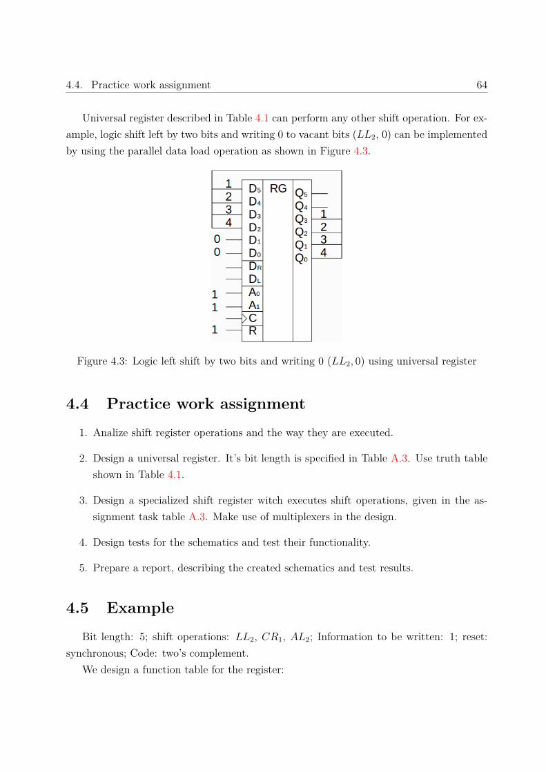
Universal register described in Table 4.1 can perform any other shift operation. For ex-ample, logic shift left by two bits and writing 0 to vacant bits (LL2, 0) can be implementedby using the parallel data load operation as shown in Figure 4.3.
Figure 4.3: Logic left shift by two bits and writing 0 (LL2, 0) using universal register
4.4 Practice work assignment
1. Analize shift register operations and the way they are executed.
2. Design a universal register. It’s bit length is specified in Table A.3. Use truth tableshown in Table 4.1.
3. Design a specialized shift register witch executes shift operations, given in the as-signment task table A.3. Make use of multiplexers in the design.
4. Design tests for the schematics and test their functionality.
5. Prepare a report, describing the created schematics and test results.
4.5 Example
Bit length: 5; shift operations: LL2, CR1, AL2; Information to be written: 1; reset:synchronous; Code: two’s complement.
We design a function table for the register:

4.5. Example 65
R A0A1 Q4 Q3 Q2 Q1 Q0 Action0 x x 0 0 0 0 0 Set logic 01 0 0 Q4 Q3 Q2 Q4 Q0 Hold state1 1 0 DR Q4 Q3 Q2 Q1 Logic shift right, writing DR(LR1, DR)1 0 1 Q3 Q2 Q1 Q0 DL Logic shift left, writing DL(LL1, DL)1 1 1 D4 D3 D2 D1 D0 Parallel data load
The register has to execute 4 shift operations, therefore we will use multiplexers. SignalsA1, A0 are connected to the multiplexer selector inputs. Data inputs are connected tosignals according to the register function table.
• For the synchronous reset, use D Flip-Flop GSR Clear fd1s3ax
• For the asynchronous reset, use D Flip-Flop Asynchronuos clear fd1s3dx
For synchronous reset we will insert an AND gate, controlled by a RESET signal.For asynchronous reset only the appropriate flip-flops are required. The schematic of theuniversal register is presented in Fig. 4.4.
Figure 4.4: Schematic of a universal register
We design a test for testing all of the register’s functions. We get timing diagrams,presented in Fig. 4.5.

4.5. Example 66
Figure 4.5: Timing diagrams of a universal register.
When designing a specialized register, which executes the following shift operationsLL2, input data:1, CR1 and AL2, we will use multiplexers with 4 inputs and flip-flops.Multiplexers are controlled by signals A0 and A1. These inputs control, which operationis being executed. We draw a table with the information needed to design the schematic.
OP codeA0 A1 D4 D3 D2 D1 D0 Action0 0 x4 x3 x2 x1 x0 Data load0 1 Q2 Q1 Q0 1 1 LL2, 11 0 Q0 Q4 Q3 Q2 Q1 CR11 1 Q4 Q1 Q0 0 0 AL2, two’s complement
Information in the table can be expressed in boolean functions:
D0 = A0A1x0 ∪ A0A11 ∪ A0A1Q1 ∪ A0A10;D1 = A0A1x1 ∪ A0A11 ∪ A0A1Q2 ∪ A0A10;D2 = A0A1x2 ∪ A0A1Q0 ∪ A0A1Q3 ∪ A0A1Q0;D3 = A0A1x3 ∪ A0A1Q1 ∪ A0A1Q4 ∪ A0A1Q1;D4 = A0A1x4 ∪ A0A1Q2 ∪ A0A1Q0 ∪ A0A1Q4;
This design is easy to implement using multiplexers, as shown in Fig. 4.6.
Figure 4.6: Schematic of a specialized register with synchronous reset

4.5. Example 67
We design a test for testing all of the register’s functions. We get timing diagrams,presented in Fig. 4.7.
Figure 4.7: Timing diagram of a specialized register
By examiming the timing diagrams, we note that the register executes all of the oper-ations required: LL2, CR1, AL2.

Appendix A
Assignment tasks
A.1 Tasks for practice work 1
Tasknr.
Function
1 0,2,5,7,13,15,21,23,25,27,44,45,46,47,57,58,61,632 8,10,13,15,17,19,29,31,36,37,38,39,41,43,45,47,53,553 0,2,21,23,25,27,29,31,40,41,42,43,48,49,53,55,61,634 1,6,20,21,26,27,28,29,41,42,43,46,49,51,52,53,60,615 8,10,17,19,21,23,32,33,34,35,45,47,53,55,56,57,61,636 9,14,18,19,20,21,32,33,34,35,44,45,52,53,57,59,60,617 0,1,7,8,9,17,18,22,23,25,47,49,50,53,54,55,57,638 1,3,5,9,11,19,21,22,23,27,45,51,52,53,54,55,59,619 8,9,15,17,24,25,39,41,47,49,50,54,55,57,58,59,62,6310 9,11,13,19,25,27,37.43,45,51,53,54,55,59,60,61,62,6311 0,6,7,14,15,22,23,24,25,26,27,30,31,45,46,55,61,6212 1,6,7,14,15,22,23,25,26,27,29,30,31,45,46,55,61,6213 3,5,7,13,15,21,23,26,27,28,29,30,31,44,47,53,60,6314 9,14,15,17,18,19,21,22,23,30,31,37,38,45,46,54,55,6315 8,10,14,16,17,18,19,22,23,26,30,34,39,42,47,50,54,6216 11,13,15,18,19,20,21,22,23,30,31,36,39,44,47,53,55,6117 2,3,5,10,11,19,20,22,28,30,52,53,54,55,60,61,62,6318 2,5,6,7,9,13,15,18,21,22,23,29,31,49,51,57,59,6219 4,5,6,7,11,12,13,20,21,22,23,28,29,50,51,58,59,63
68
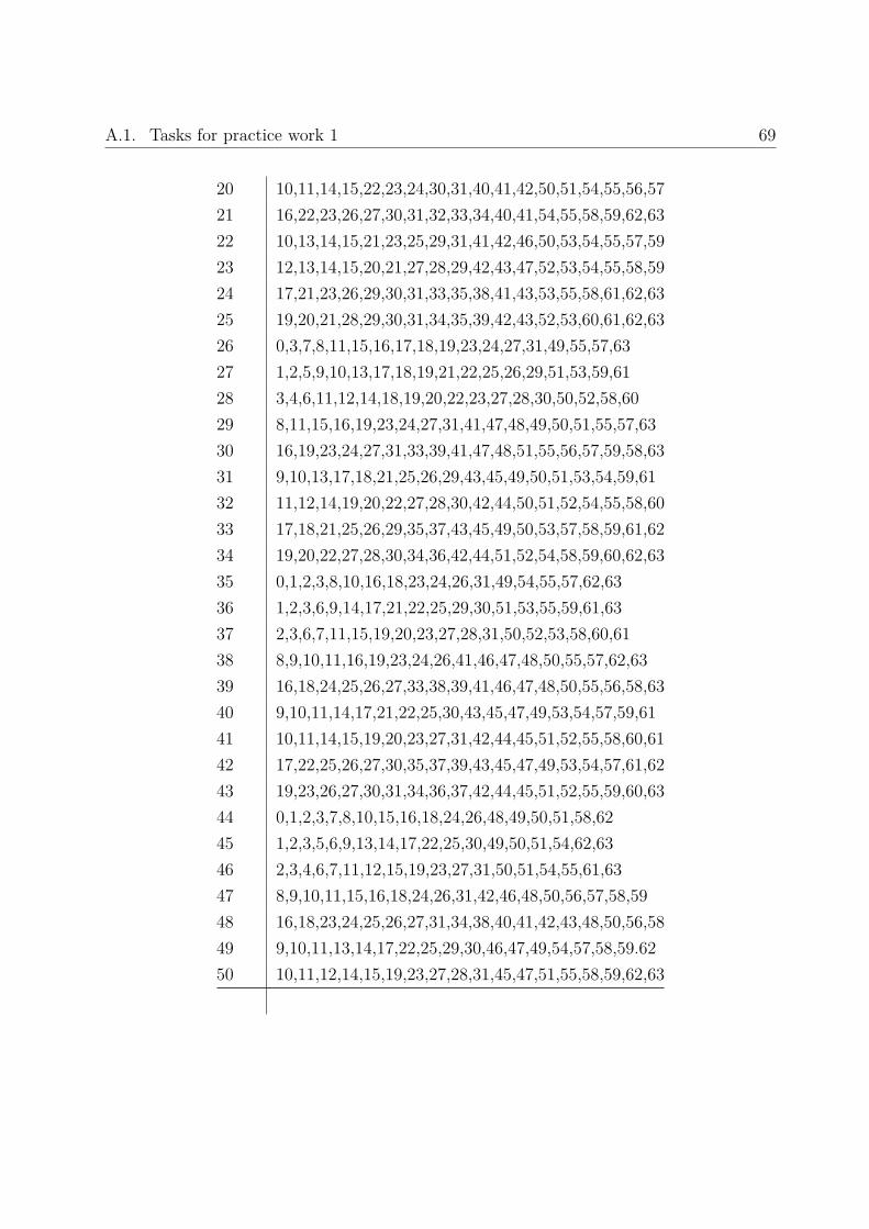
A.1. Tasks for practice work 1 69
20 10,11,14,15,22,23,24,30,31,40,41,42,50,51,54,55,56,5721 16,22,23,26,27,30,31,32,33,34,40,41,54,55,58,59,62,6322 10,13,14,15,21,23,25,29,31,41,42,46,50,53,54,55,57,5923 12,13,14,15,20,21,27,28,29,42,43,47,52,53,54,55,58,5924 17,21,23,26,29,30,31,33,35,38,41,43,53,55,58,61,62,6325 19,20,21,28,29,30,31,34,35,39,42,43,52,53,60,61,62,6326 0,3,7,8,11,15,16,17,18,19,23,24,27,31,49,55,57,6327 1,2,5,9,10,13,17,18,19,21,22,25,26,29,51,53,59,6128 3,4,6,11,12,14,18,19,20,22,23,27,28,30,50,52,58,6029 8,11,15,16,19,23,24,27,31,41,47,48,49,50,51,55,57,6330 16,19,23,24,27,31,33,39,41,47,48,51,55,56,57,59,58,6331 9,10,13,17,18,21,25,26,29,43,45,49,50,51,53,54,59,6132 11,12,14,19,20,22,27,28,30,42,44,50,51,52,54,55,58,6033 17,18,21,25,26,29,35,37,43,45,49,50,53,57,58,59,61,6234 19,20,22,27,28,30,34,36,42,44,51,52,54,58,59,60,62,6335 0,1,2,3,8,10,16,18,23,24,26,31,49,54,55,57,62,6336 1,2,3,6,9,14,17,21,22,25,29,30,51,53,55,59,61,6337 2,3,6,7,11,15,19,20,23,27,28,31,50,52,53,58,60,6138 8,9,10,11,16,19,23,24,26,41,46,47,48,50,55,57,62,6339 16,18,24,25,26,27,33,38,39,41,46,47,48,50,55,56,58,6340 9,10,11,14,17,21,22,25,30,43,45,47,49,53,54,57,59,6141 10,11,14,15,19,20,23,27,31,42,44,45,51,52,55,58,60,6142 17,22,25,26,27,30,35,37,39,43,45,47,49,53,54,57,61,6243 19,23,26,27,30,31,34,36,37,42,44,45,51,52,55,59,60,6344 0,1,2,3,7,8,10,15,16,18,24,26,48,49,50,51,58,6245 1,2,3,5,6,9,13,14,17,22,25,30,49,50,51,54,62,6346 2,3,4,6,7,11,12,15,19,23,27,31,50,51,54,55,61,6347 8,9,10,11,15,16,18,24,26,31,42,46,48,50,56,57,58,5948 16,18,23,24,25,26,27,31,34,38,40,41,42,43,48,50,56,5849 9,10,11,13,14,17,22,25,29,30,46,47,49,54,57,58,59.6250 10,11,12,14,15,19,23,27,28,31,45,47,51,55,58,59,62,63

A.2. Tasks for practice work 2 70
A.2 Tasks for practice work 2
Task. Type Schematic SynchronizationNr. signals1 SR 3.14 a C1 C2
2 JK 3.14 b C1 C2
3 D 3.14 b C1 C2
4 SR 3.14 a C1 C2
5 JK 3.14 a C1 C2
6 D 3.14 b C1 C2
7 SR 3.14 b C1 C2
8 JK 3.14 a C1 C2
9 D 3.14 a C1 C2
10 SR 3.14 b C1 C2
11 JK 3.14 b C1 C2
12 D 3.14 a C1 C2
13 SR 3.14 a C1 C2
14 JK 3.14 b C1 C2
15 D 3.14 b C1 C2
16 SR 3.14 a C1 C2
17 JK 3.14 a C1 C2
18 D 3.14 b C1 C2
19 SR 3.14 b C1 C2
20 JK 3.14 a C1 C2
21 D 3.14 a C1 C2
22 SR 3.14 b C1 C2
23 JK 3.14 b C1 C2
24 D 3.14 a C1 C2
25 SR 3.14 a C1 C2
26 JK 3.14 b C1 C2
27 D 3.14 b C1 C2
28 SR 3.14 b C1 C2
29 JK 3.14 b C1 C2
30 D 3.14 a C1 C2
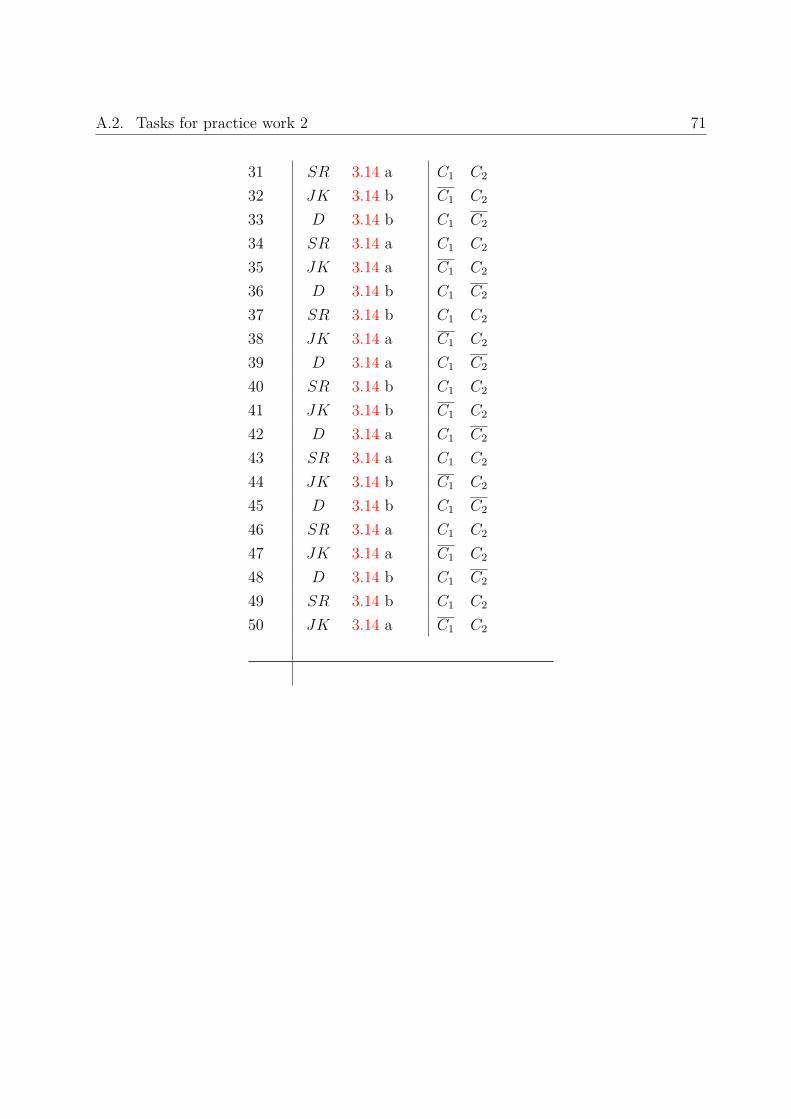
A.2. Tasks for practice work 2 71
31 SR 3.14 a C1 C2
32 JK 3.14 b C1 C2
33 D 3.14 b C1 C2
34 SR 3.14 a C1 C2
35 JK 3.14 a C1 C2
36 D 3.14 b C1 C2
37 SR 3.14 b C1 C2
38 JK 3.14 a C1 C2
39 D 3.14 a C1 C2
40 SR 3.14 b C1 C2
41 JK 3.14 b C1 C2
42 D 3.14 a C1 C2
43 SR 3.14 a C1 C2
44 JK 3.14 b C1 C2
45 D 3.14 b C1 C2
46 SR 3.14 a C1 C2
47 JK 3.14 a C1 C2
48 D 3.14 b C1 C2
49 SR 3.14 b C1 C2
50 JK 3.14 a C1 C2

A.3. Tasks for practice work 3 72
A.3 Tasks for practice work 3
Taskno.
Bit length Shift operations Inputinfor-mation
Reset Representation
1 6 LR1, CL2, AL1 0 Synchronous Sign-and-magnitude
2 7 LL1, CR2, AR1 1 Asynchronous one’s comple-ment
3 8 LR2, CL1, AL2 0 Asynchronous two’s comple-ment
4 6 LL2, CR1,AR2 1 Synchronous one’s comple-ment
5 7 LR1, CR2, AL2 0 Synchronous two’s comple-ment
6 8 LL1, CL1, AR2 1 Asynchronous Sign-and-magnitude
7 6 LR2, CR1, AL1 0 Asynchronous two’s comple-ment
8 7 LL2, CL2, AR1 1 Synchronous Sign-and-magnitude
9 8 LR1, CL1, AL2 0 Synchronous one’s comple-ment
10 6 LL1, CR1, AR2 1 Asynchronous Sign-and-magnitude
11 7 LR2, CL2, AL1 0 Asynchronous one’s comple-ment
12 8 LL2, CR2, AR1 1 Synchronous two’s comple-ment
13 6 LR1, CR1, AL2 0 Synchronous one’s comple-ment
14 7 LL1, CL2, AR2 1 Asynchronous two’s comple-ment

A.3. Tasks for practice work 3 73
15 8 LR1, CR2, AL1 0 Asynchronous Sign-and-magnitude
16 6 LL2, CL1, AR1 1 Synchronous two’s comple-ment
17 7 LR1, CL2, AR1 0 Synchronous Sign-and-magnitude
18 8 LL1, CR2, AL1 1 Asynchronous one’s comple-ment
19 6 LR2, CL1, AR2 0 Asynchronous Sign-and-magnitude
20 7 LL2, CR1, AL2 1 Synchronous one’s comple-ment
21 8 LR1, CR2, AR2 0 Synchronous two’s comple-ment
22 6 LL1, CL1, AL2 1 Asynchronous one’s comple-ment
23 7 LR2, CR1,AR1 0 Asynchronous two’s comple-ment
24 8 LR1, CL2, AL1 1 Synchronous Sign-and-magnitude
25 6 LL1, CR2, AR1 0 Synchronous two’s comple-ment
26 7 LR2, CL1, AL2 1 Asynchronous Sign-and-magnitude
27 8 LL2, CR1,AR2 0 Asynchronous one’s comple-ment
28 6 LR1, CR2, AL2 1 Synchronous Sign-and-magnitude
29 7 LL1, CL1, AR2 0 Synchronous one’s comple-ment
30 8 LR2, CR1, AL1 1 Asynchronous two’s comple-ment
31 6 LL2, CL2, AR1 0 Asynchronous one’s comple-ment

A.3. Tasks for practice work 3 74
32 7 LR1, CL1, AL2 1 Synchronous two’s comple-ment
33 8 LL1, CR1, AR2 0 Synchronous Sign-and-magnitude
34 6 LR2, CL2, AL1 1 Asynchronous two’s comple-ment
35 7 LL2, CR2, AR1 0 Asynchronous Sign-and-magnitude
36 8 LR1, CR1, AL2 1 Synchronous one’s comple-ment
37 6 LL1, CL2, AR2 0 Synchronous Sign-and-magnitude
38 7 LR1, CR2, AL1 1 Asynchronous one’s comple-ment
39 8 LL2, CL1, AR1 0 Asynchronous two’s comple-ment
40 6 LR1, CL2, AR1 1 Synchronous one’s comple-ment
41 7 LL1, CR2, AL1 0 Synchronous two’s comple-ment
42 8 LR2, CL1, AR2 1 Asynchronous Sign-and-magnitude
43 6 LL2, CR1, AL2 0 Asynchronous two’s comple-ment
44 7 LR1, CR2, AR2 1 Synchronous Sign-and-magnitude
45 8 LL1, CL1, AL2 0 Synchronous one’s comple-ment
46 6 LR2, CR1,AR1 1 Asynchronous Sign-and-magnitude
47 7 LR1, CL2, AL1 0 Asynchronous one’s comple-ment
48 8 LL1, CR2, AR1 1 Synchronous two’s comple-ment

A.3. Tasks for practice work 3 75
49 6 LR2, CL1, AL2 0 Synchronous one’s comple-ment
50 7 LL2, CR1,AR2 1 Asynchronous two’s comple-ment