automotive, four-channel, class d amplifier reference
TRANSCRIPT

0
10
20
30
40
50
60
70
80
90
100
0 2 4 6 8 10 12 14 16 18 20 22 24 26 28 30 32
Effic
iency
(%)
Power per Channel (W)
TAS5404-Q1 only
System Efficiency
C001
Second-OrderLC Filter
5.6- to 18-VOperation
TL760M33-Q13.3-V LDO
OSC EEPROM
TAS1020BUSB Controller
PC (GUI)
I2C
Daughterboard
TAS5404-Q1Four-Channel
Class DAmplifier
PVDD = 5.6 V to 18 V
3.3 V
Second-Order
LC Filter
Four-ChannelBTL
AnalogOutput
First-OrderRC Filter
Four AudioAnalogInput
TI DesignsAutomotive, Four-Channel, Class D Amplifier ReferenceDesign for Head Unit
Design Overview Design FeaturesThis design provides a Class D-based amplifier • Withstands Load-Dump Conditionssolution that allows it to be evaluated in the form factor • Size and Space Optimized Designof a typical Class AB amplifier. The design is optimized
• CISPR-25 Tested EMIto mitigate thermals associated with audio amplifiers• Withstands Start/Stop Operation Down to 5.6 Vand to minimize switching noises associated with
Class D amplifiers. This design consists of two circuitFeatured Applicationsboards. The first board highlights the audio amplifier
module. The second board highlights circuitry to • Automotive Color Media or Display Audioincorporate the amplifier module into a base board.
• Automotive Mid- and Low-Head UnitsThe pair of boards allows stand-alone performancetesting of the design. • Automotive Seat Vibration
• Audio Amplifier ModulesDesign Resources
Tool Folder Containing Design FilesTIDA-00573TAS5404-Q1 Product FolderTL760M33-Q1 Product Folder
ASK Our E2E Experts
1TIDUB81–January 2016 Automotive, Four-Channel, Class D Amplifier Reference Design for HeadUnitSubmit Documentation Feedback
Copyright © 2016, Texas Instruments Incorporated

System Description www.ti.com
An IMPORTANT NOTICE at the end of this TI reference design addresses authorized use, intellectual property matters and otherimportant disclaimers and information.
1 System DescriptionThis system has been designed to be a form, fit, and functional evaluation of the typical configuration ofClass AB amplifiers in an integrated amplifier head unit. To accommodate this purpose, the followingdesign points have been considered:• Support of the vertical profile of the audio amplifier to allow it to use the metal housing of an existing
head unit as a heat sink• Off-battery voltage support including line noise filters that receive power from the reverse battery
protection circuit incorporated off of the base board• Speaker drive filter integration to eliminate noise coupling into the AM radio band
To ease the design of this module into a head unit base board, a companion board has been included.This board highlights the decoupling capacitors, analog input noise filters, and the appropriate layoutconsiderations for incorporating the module into the design (see Figure 1).
Figure 1. Automotive Head Unit With Integrated Display Example Highlighting TIDA-00573
2 Automotive, Four-Channel, Class D Amplifier Reference Design for Head TIDUB81–January 2016Unit Submit Documentation Feedback
Copyright © 2016, Texas Instruments Incorporated

www.ti.com Key System Specifications
2 Key System Specifications
Table 1. Audio Module System Specifications
PARAMETER COMMENTS MIN TYP MAX UNITSystem input
VIN Operational input voltage Battery voltage range audio amp is functional (DC) 5.6 14 18 VMaximum battery voltage on the module withoutVMAX Maximum input Voltage –0.3 30 Vdevice damage
ISTDBY Input current All four channels in MUTE mode 170 220 mAAudio inputVAIN Maximum audio input voltage 19 VRMS
VLOGIC Input voltage range for IO pins I2C lines, MUTE, standby –0.3 6 VAudio performance (VIN = 14.4 V)POUT Output power per channel 4-Ω speaker load driven 22 WPEFF Power efficiency 4-Ω speaker load driven 90 %
PSRR Power supply rejection 1-VRMS ripple on 14.4-V supply 75 dBTHD Total harmonic distortion 1-W output 0.02 %
ThermalsMaximum operating junctionTJ TAS5404-Q1 junction temperature –55 150 °Ctemperature
3TIDUB81–January 2016 Automotive, Four-Channel, Class D Amplifier Reference Design for HeadUnitSubmit Documentation Feedback
Copyright © 2016, Texas Instruments Incorporated

Second-OrderLC Filter
5.6- to 18-VOperation
TL760M33-Q13.3-V LDO
OSC EEPROM
TAS1020BUSB Controller
PC (GUI)
I2CDaughterboard
TAS5404-Q1Four-Channel
Class DAmplifier
PVDD = 5.6 V to 18 V
3.3 V
Second-Order
LC Filter
Four-ChannelBTL
AnalogOutput
First-OrderRC Filter
Four AudioAnalogInput
Block Diagram www.ti.com
3 Block Diagram
Figure 2. Automotive, Four-Channel, Class D Amplifier for Head Unit
3.1 Highlighted ProductsThe TIDA-00573 design uses the following TI products:• TAS5404-Q1: This device is a four-channel digital audio amplifier with an input voltage range from
5.6 V to 18 V (50-V load dump), which enables it to work directly from an automotive battery.• TL760M33-Q1: This device is a low-dropout regulator (LDO) with several fixed-voltage options with the
capability of sourcing 500 mA of current. This device has been added to the design to showcase theinteraction of the Class D amplifiers with a head unit; therefore, this document does not describe it infull detail.
• TAS1020B: This device is a universal serial bus (USB) peripheral interface device for isochronous datastreaming. In this design, the TAS1020B connects the graphical user interface (GUI) to the board toset the I2C address, data, and diagnostics for the TAS5404-Q1. This device performs functionsnormally performed by the system microcontroller or processor in a complete system and has beenincluded for no other purpose than to demonstrate the TAS5404-Q1 capabilities; therefore, thisdocument does not describe it in full detail. Note that the TAS1020B is not AEC Q100 qualified.Texas Instruments (TI) does not recommend the use of this device for new designs.
4 Automotive, Four-Channel, Class D Amplifier Reference Design for Head TIDUB81–January 2016Unit Submit Documentation Feedback
Copyright © 2016, Texas Instruments Incorporated

www.ti.com Block Diagram
3.1.1 TAS5404-Q1
Figure 3. 25-W, Analog, Single-Ended Input, 4-Ch, Class D Amp With Load Dump Protectionand I2C Diagnostics
• Output power: 4 W × 22 W at 4 Ω, 1% THD+N, 14.4 V• Input range 5.6 V to 18 V (operational during cold, crank, start, and stop events)• 50-V load dump and over temperature protection• Automotive electromagnetic interference (EMI) performance (CISPR25 Class 5)• I2C load diagnostics (shorts, open, and tweeter)• Programmable switching frequency (357 kHz, 417 kHz, and 500 kHz) for AM band avoidance• Lineout mode: From a few Ω to several kΩ• Fully AEC-Q100 qualified and TS16949 certified
3.1.2 TL760M33-Q1• Load-dump protection• Qualified for automotive applications• ±3% output voltage variation across load and temperature• 500-mV maximum dropout voltage at 500 mA• Fixed 3.3-V output• Internal thermal overload protection• Internal overvoltage protection
5TIDUB81–January 2016 Automotive, Four-Channel, Class D Amplifier Reference Design for HeadUnitSubmit Documentation Feedback
Copyright © 2016, Texas Instruments Incorporated

System Design www.ti.com
4 System DesignAs the block diagram in the previous Figure 1 shows, the design consists of two separate parts: adaughterboard (see Figure 4) and a motherboard (see Figure 5), which have been soldered togetherthrough the dual row connector.
Figure 4. Daughterboard—3D View
The daughterboard encompasses the Class D amplifier solution in a small form factor comparable toClass AB devices. The motherboard is a base board simulating a part that is normally in the head unit toshow the functionality of the daughterboard.
Figure 5. Motherboard—3D View
6 Automotive, Four-Channel, Class D Amplifier Reference Design for Head TIDUB81–January 2016Unit Submit Documentation Feedback
Copyright © 2016, Texas Instruments Incorporated
( )2
BTL 2
2 0.707 10C 0.62 F
4
´ ´ m= = m
4L 10 H
4 45000 0.707= = m
p ´ ´
BTLBTL
c
RL
4 f Q=
p
2BTL
BTL g 2BTL
2Q LC C
R= =
www.ti.com System Design
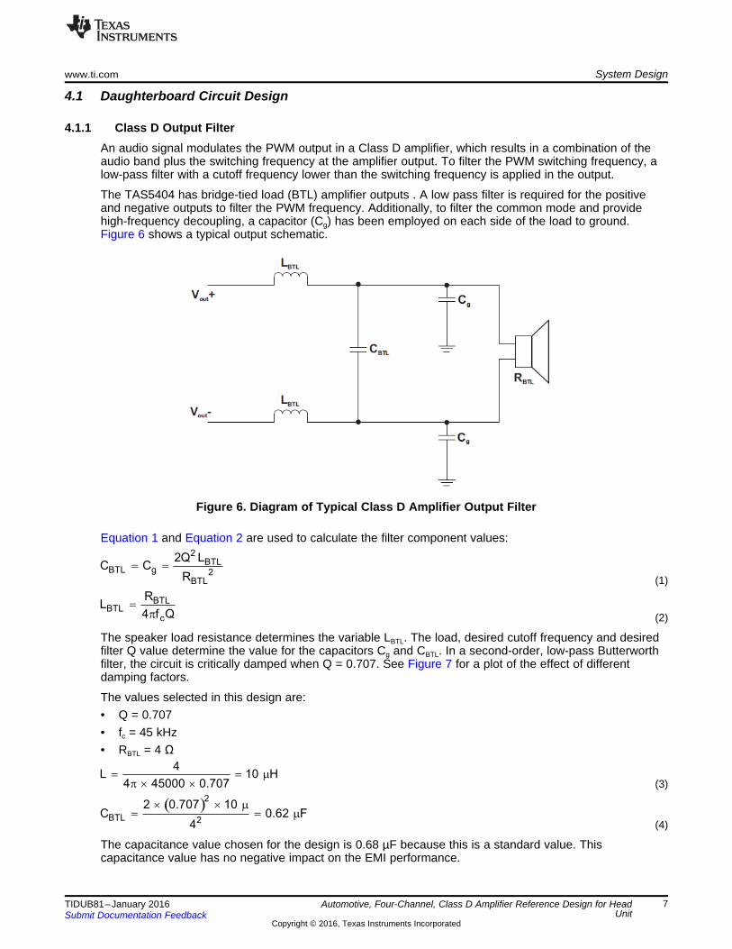
4.1 Daughterboard Circuit Design
4.1.1 Class D Output FilterAn audio signal modulates the PWM output in a Class D amplifier, which results in a combination of theaudio band plus the switching frequency at the amplifier output. To filter the PWM switching frequency, alow-pass filter with a cutoff frequency lower than the switching frequency is applied in the output.
The TAS5404 has bridge-tied load (BTL) amplifier outputs . A low pass filter is required for the positiveand negative outputs to filter the PWM frequency. Additionally, to filter the common mode and providehigh-frequency decoupling, a capacitor (Cg) has been employed on each side of the load to ground.Figure 6 shows a typical output schematic.
Figure 6. Diagram of Typical Class D Amplifier Output Filter
Equation 1 and Equation 2 are used to calculate the filter component values:
(1)
(2)
The speaker load resistance determines the variable LBTL. The load, desired cutoff frequency and desiredfilter Q value determine the value for the capacitors Cg and CBTL. In a second-order, low-pass Butterworthfilter, the circuit is critically damped when Q = 0.707. See Figure 7 for a plot of the effect of differentdamping factors.
The values selected in this design are:• Q = 0.707• fc = 45 kHz• RBTL = 4 Ω
(3)
(4)
The capacitance value chosen for the design is 0.68 µF because this is a standard value. Thiscapacitance value has no negative impact on the EMI performance.
7TIDUB81–January 2016 Automotive, Four-Channel, Class D Amplifier Reference Design for HeadUnitSubmit Documentation Feedback
Copyright © 2016, Texas Instruments Incorporated

OUT2+
OUT2-
470pF
C19
470pF
C22
0.47µF
C20
0.47µF
C23
5.6
R12
5.6
R13
CPC_TOP42
GND43
OUT2_P44
OUT2_M45
GND46
OUT1_P47
10µHL5
DFEG7030D-100M
10µHL6DFEG7030D-100M
0.68µFC21
System Design www.ti.com
Figure 7. Filter Damping (Q Factor)
Figure 8 shows a schematic for one output channel with the inductor and capacitor values calculated fromEquation 1 and Equation 2.
Figure 8. Output Filter in OUT2
4.1.2 Metal Alloy InductorsOne of the key parameters for this design is the total size of the daughterboard. The use of smallinductors is desirable because they reduce circuit board size. Metal alloy inductors present benefits ofsmaller size, better temperature stability, higher current capability, and low leakage flux in comparison toferrite inductors, which are typically used in circuits.
As the following Figure 9 shows, the variation of inductance is not significant as the temperature rises.This characteristic makes metal alloy inductors very stable over temperature. The inductance drop is smallover a larger current swing. This characteristic is necessary in Class D amplifiers to maintain inductance inthe output filter over all current levels. If the inductance drops to a low level, the overcurrent protectionmay trigger unexpectedly.
8 Automotive, Four-Channel, Class D Amplifier Reference Design for Head TIDUB81–January 2016Unit Submit Documentation Feedback
Copyright © 2016, Texas Instruments Incorporated

www.ti.com System Design
Figure 9. Inductance Versus Current in Metal Alloy Inductor
4.2 Motherboard Circuit DesignThe motherboard encompasses what is typically included in a head unit and has been designed toshowcase the performance of the daughterboard.
The motherboard features:• Input filter• USB controller• Basic GUI for diagnostics• Power management• Input and output connectors
4.2.1 Input FilterThe input filter features the DC blocking caps; a first-order, low-pass RC filter towards the input a decadeabove the audio band; and a first-order, low-pass RC filter towards the connector for the return signal thatthe user may receive from the device.
One important thing to note is that the total impedance of the input must match the impedance of thereturn input on the TAS5404-Q1 device (IN_M) as specified in the TAS5404-Q1 datasheet SLOS918.
Figure 10 shows jumpers J3 and J4 that have been provided to tie the right channels and left channelstogether, which allows the user to drive the four Class D amplifiers with only one stereo jack input.
9TIDUB81–January 2016 Automotive, Four-Channel, Class D Amplifier Reference Design for HeadUnitSubmit Documentation Feedback
Copyright © 2016, Texas Instruments Incorporated

5
4
1
2
3
6
7
8
J5
OUT2+
OUT2-
OUT1+
OUT1-
OUT3+
OUT3-
OUT4+
OUT4-
0.01µFC521
0.01µFC522
0.01µFC511
0.01µFC512
0.01µFC531
0.01µFC532
0.01µFC541
0.01µFC542
GND GND GND GND GND GND GND GND
3
2
1
J1
SJ-3523-SMT
IN1
IN2
49.9kR11
49.9kR12
499
R1
499
R2
499
R5
499
R6
1200pFC7
1200pFC8
GND
GND
GND
Right
Left
0.47µF
C1
0.47µF
C2
1
2
J3
PEC02SAAN
1
2
J4
PEC02SAAN
System Design www.ti.com
Figure 10. Input Filter
4.2.2 Output Connector and FilterTo filter high frequencies and improve EMI performance, capacitors have been added next to the outputconnector, which creates a low-impedance path for high frequency signals (see Figure 11).
Figure 11. Filter at Connector
10 Automotive, Four-Channel, Class D Amplifier Reference Design for Head TIDUB81–January 2016Unit Submit Documentation Feedback
Copyright © 2016, Texas Instruments Incorporated

www.ti.com Getting Started
5 Getting StartedThe following procedure assumes that the TAS1020B (U2 on the USB board) is populated.
To get started with the TIDA-00573, connect the power leads to the four-terminal connector (J8) in thelabeled polarity shown in Figure 12. TI recommends using two wires for each power connection. Note thatthe screw terminal accepts 22 AWG wire.
Connect a power supply to the leads. Do not turn on the power supply at this point.
Figure 12. Step 1—VIN Input Connection
Connect the USB cable to the PC and J9 through the micro-USB connector (see Figure 13). Make surethat the jumper in J7 has been removed and that switch S1 has been set for NORMAL operation.
Figure 13. Step 2—Micro-USB Connection
Connect the loads or speakers through the J8 output connectors. Note that the plus and minus of everychannel are labeled and the order of the channels from top to bottom is 2, 1, 3, 4. These terminals accept22 AWG wires.
Connect the input 3.5-mm female jack to the input connectors. The user can short the two stereo jacksusing jumpers in J3 and J4 as discussed in Section 4.2.1 This ties the right and left channels together sothat only one stereo jack is required to provide a signal to the four channels of the amplifier.
Now set the power supply to the desired voltage (typically 14.4 V) and apply power to the TIDA-00573.The green light-emitting diode (LED) D4 labeled “3.3V” and the blue LED D3 labeled “USB” should nowturn on. After this step, the board is ready to be controlled by the GUI.
11TIDUB81–January 2016 Automotive, Four-Channel, Class D Amplifier Reference Design for HeadUnitSubmit Documentation Feedback
Copyright © 2016, Texas Instruments Incorporated

Graphical User Interface www.ti.com
6 Graphical User InterfaceThe following procedure assumes that the TAS1020B (U2 on the USB board) has been populated.
The GUI utilizes the TI Purepath™ Console 3 (PPC3) Software. Download the GUI fromhttp://www.ti.com/tool/PUREPATHCONSOLE.
The TAS5404Q1EVM GUI is downloadable through the PPC3 platform. Any updates automatically displayfor download. Connect the PC to the internet to use this function.
Figure 14 displays the GUI. Connect the GUI to the EVM by clicking the Connect button at the bottom leftof interface. Upon a successful connection the small circle turns green and the Connect buttondisappears.
Figure 14. TAS5404 EVM GUI Home Page
6.1 Register Map PageClick on the Register Map menu heading located at the top of the Home page to display the register mapof the TAS5404-Q1 device. Opening the page reads all registers and populates the registers with theTAS5404-Q1 register defaults.
Figure 15 displays the Register Map page. Click on the register to display the description in the Fieldscolumn. In the Register Map table, the pink values are read only and the black values can be changedand written to the device. Double click on a black value to change its state and write the value to thedevice. Reference the TAS5404-Q1 datasheet, SLOS918, for complete descriptions of the registers andtheir functions.
Click on the TAS5404 EVM Home menu heading above the Register Map table to return to the Homepage.
12 Automotive, Four-Channel, Class D Amplifier Reference Design for Head TIDUB81–January 2016Unit Submit Documentation Feedback
Copyright © 2016, Texas Instruments Incorporated

www.ti.com Graphical User Interface
Figure 15. Register Map Page
6.2 Device Control PageEnter the Device Control page by clicking on the Device Control menu heading located at the top of theHome page. The page shown by Figure 16 displays. This page has buttons that control certain functionsof the TAS5404-Q1 device.
Figure 16. Device Control Page
13TIDUB81–January 2016 Automotive, Four-Channel, Class D Amplifier Reference Design for HeadUnitSubmit Documentation Feedback
Copyright © 2016, Texas Instruments Incorporated

OUT2+
OUT2-
470pF
C19
470pF
C22
0.47µF
C20
0.47µF
C23
5.6
R12
5.6
R13
CPC_TOP 42
GND 43
OUT2_P 44
OUT2_M 45
GND 46
OUT1_P 47
10µH L5DFEG7030D-100M
10µH L6DFEG7030D-100M
0.68µFC21
PCB Layout Guidelines www.ti.com
7 PCB Layout GuidelinesSeveral critical items must be considered in the circuit board layout to optimize noise and EMIperformance:• A heatsink must make contact with the top of the amplifier IC. Ensure that components placed nearby
do not interfere with the heatsink.• The decoupling capacitors must be physically close to the TAS5404-Q1. The decoupling capacitors are
C10, C11, C37, and C38 in this design (see Figure 19).• The snubber circuits must be placed as close as possible to the TAS5404-Q1 to reduce the AC current
path (see Figure 17).
Figure 17. AC Current Path in Snubber Circuits
• The common-mode filter capacitors C20 and C23 must share a common ground in the same plane.The ground pins for these capacitors must be placed very close to a via to minimize the loopinductance for these capacitors (see Figure 18).
Figure 18. Common-Mode Capacitors Layout
• TI recommends via stitching across the entire ground plane to reduce the ground impedance.• TI recommends that the output filter inductors be placed close to the TAS5404-Q1 to reduce the trace
impedance.
14 Automotive, Four-Channel, Class D Amplifier Reference Design for Head TIDUB81–January 2016Unit Submit Documentation Feedback
Copyright © 2016, Texas Instruments Incorporated

SnubbersOUT1OUT2OUT3OUT4
www.ti.com PCB Layout Guidelines
The boxed-in areas in Figure 19 indicate the outputs. The image on the left side of the figure emphasizesthe output filters and the right-side image shows the snubber circuits.
Figure 19. Placement of Components—Daughterboard
The grounding between the signal inputs on the motherboard and the daughterboard has been reinforcedby a trace that connects them to avoid any difference in the grounding created by the resistance of theconnector or interferences from other signals (see Figure 20). With the purpose of avoiding a difference inthe grounding between the daughterboard and the signal inputs on the motherboard created by theresistance of the connector or interferences from other signals, this ground was reinforced by a traceconnecting them.
Figure 20. Ground Trace on Bottom Layer
15TIDUB81–January 2016 Automotive, Four-Channel, Class D Amplifier Reference Design for HeadUnitSubmit Documentation Feedback
Copyright © 2016, Texas Instruments Incorporated

PCB Layout Guidelines www.ti.com
TI recommends routing the amplifier output + and – signals on adjacent layers with the traces overlappedas much as possible. Routing the signals in this way helps to cancel EMI from the output sections.Keeping the output routes on inner layers of the circuit board also improves EMI performance if the outerlayers have ground fills over the traces. Figure 21 shows the routing of the output signals.
Figure 21. Output Signal Traces Overlap for Current Cancellation in Layer 2 and Layer 3
16 Automotive, Four-Channel, Class D Amplifier Reference Design for Head TIDUB81–January 2016Unit Submit Documentation Feedback
Copyright © 2016, Texas Instruments Incorporated
20 200 2k 20k 0.01
0.1
1
10
TH
D+
N (
%)
Frequency (Hz) C003
20 200 2k 20k -100
-90
-80
-70
-60
-50
-40
-30
-20C
ross
talk
(dB
)
Frequency (Hz) C006
www.ti.com Test Results
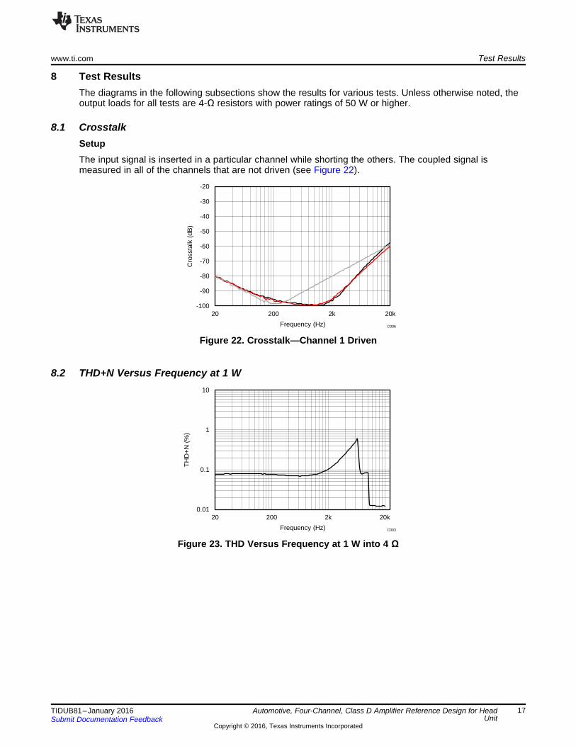
8 Test ResultsThe diagrams in the following subsections show the results for various tests. Unless otherwise noted, theoutput loads for all tests are 4-Ω resistors with power ratings of 50 W or higher.
8.1 CrosstalkSetupThe input signal is inserted in a particular channel while shorting the others. The coupled signal ismeasured in all of the channels that are not driven (see Figure 22).
Figure 22. Crosstalk—Channel 1 Driven
8.2 THD+N Versus Frequency at 1 W
Figure 23. THD Versus Frequency at 1 W into 4 Ω
17TIDUB81–January 2016 Automotive, Four-Channel, Class D Amplifier Reference Design for HeadUnitSubmit Documentation Feedback
Copyright © 2016, Texas Instruments Incorporated

0
10
20
30
40
50
60
70
80
90
100
0 2 4 6 8 10 12 14 16 18 20 22 24 26 28 30 32
Effic
iency
(%)
Power per Channel (W)
TAS5404-Q1 only
System Efficiency
C001
0.01
0.1
1
10
0.1 1 10 100
TH
D+
N (
%)
Power (W) C004
Test Results www.ti.com
8.3 THD+N Versus Power at 1 kHz
Figure 24. THD+N Versus BTL Output Power at 1 kHz into 4 Ω
8.4 EfficiencyThe following Figure 25 shows the efficiency measurements for the device (TAS5404-Q1) and theTIDA-00573 board.
Figure 25. Efficiency of Device and System
18 Automotive, Four-Channel, Class D Amplifier Reference Design for Head TIDUB81–January 2016Unit Submit Documentation Feedback
Copyright © 2016, Texas Instruments Incorporated

www.ti.com Test Results
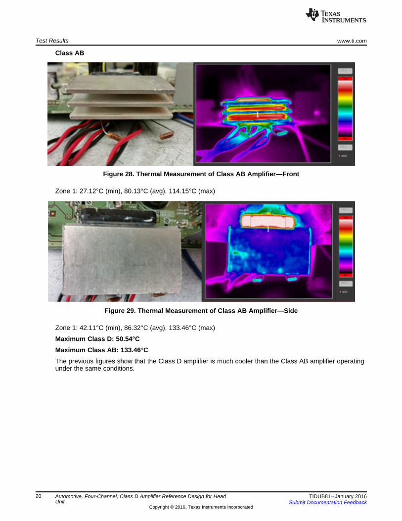
8.5 ThermalTo analyze the thermal performance of the design, a comparison with a class AB amplifier has beenconducted using the exact same heatsink and running the four channels simultaneously at 1 W. The unitsfor temperature are in °C. The thermal tests have been conducted at an ambient temperature of 25°C.
Class D
Figure 26. Thermal Measurement of Class D Amplifier—Front
Zone 1: 28.89°C (min), 36.20°C (avg), 42.32°C (max)
Zone 2: 45.75°C (min), 46.91°C (avg), 48.78°C (max)
Figure 27. Thermal Measurement of Class D Amplifier—Side
Zone 1: 24.00°C (min), 29.57°C (avg), 39.85°C (max)
Zone 2: 27.40°C (min), 38.73°C (avg), 44.93°C (max)
Zone 3: 26.47°C (min), 44.01°C (avg), 50.54°C (max)
19TIDUB81–January 2016 Automotive, Four-Channel, Class D Amplifier Reference Design for HeadUnitSubmit Documentation Feedback
Copyright © 2016, Texas Instruments Incorporated
Test Results www.ti.com
Class AB
Figure 28. Thermal Measurement of Class AB Amplifier—Front
Zone 1: 27.12°C (min), 80.13°C (avg), 114.15°C (max)
Figure 29. Thermal Measurement of Class AB Amplifier—Side
Zone 1: 42.11°C (min), 86.32°C (avg), 133.46°C (max)
Maximum Class D: 50.54°CMaximum Class AB: 133.46°CThe previous figures show that the Class D amplifier is much cooler than the Class AB amplifier operatingunder the same conditions.
20 Automotive, Four-Channel, Class D Amplifier Reference Design for Head TIDUB81–January 2016Unit Submit Documentation Feedback
Copyright © 2016, Texas Instruments Incorporated

www.ti.com Test Results
8.6 Load Dump Test—ISO7637 Pulse 5bThe board has been designed to withstand a 50-V load dump pulse in accordance with ISO7637-2:2004Pulse 5b specification. According to the specification, this transient occurs in the event of a dischargedbattery being disconnected while the alternator is generating charging current and with other loadsremaining on the alternator circuit.
Figure 30 shows the load dump profile. The test has been performed in the worst case scenario for a 12-Vbattery:• VIN = 14.4 V• US = 87V• td = 400 ms• tr = 10 ms• Suppressed voltage (US*) = 35.6 V
Figure 30. Load Dump Pulse 5b Configuration
A stress test of 100 repetitions with the aforementioned configuration has been conducted without causingany damage or causing the device to fail.
21TIDUB81–January 2016 Automotive, Four-Channel, Class D Amplifier Reference Design for HeadUnitSubmit Documentation Feedback
Copyright © 2016, Texas Instruments Incorporated

Test Results www.ti.com
8.7 CISPR 25 Class 5—EMI TestAutomotive infotainment equipment designers have been reluctant to use Class D amplifiers in theirsystems because of EMI concerns. This TI Design has been tested to CISPR 25 Class 5 limits toeliminate these concerns. Table 2 shows the specification limits, measured values, and margin at whichthe design passes the CISPR 25 Level 5 specification.
Table 2. CISPR 25 Limits and Test Results
LEVEL IN dB (uV/m)FREQUENCYSERVICE/BAND (MHz) CISPR 25 CLASS 5 LIMITS MEASURED VALUESBROADCAST PEAK AVERAGE AVERAGE MARGIN
LW 0.15 to 0.30 46 26 22.4 3.6MW 0.53 to 1.8 40 20 17.9 2.1SW 5.9 to 6.2 40 20 5 15FM 76 to 108 38 18 5 13
TV band I 41 to 88 28 18 4 14TV band III 174 to 230 32 22 4 18
DAB III 171 to 245 26 16 4 12TV band IV/V 468 to 944 41 31 11 20
DTTV 470 to 770 45 35 15 20DAB L band 1447 to 1494 28 18 3 15
SDARS 2320 to 2345 34 24 6 18
22 Automotive, Four-Channel, Class D Amplifier Reference Design for Head TIDUB81–January 2016Unit Submit Documentation Feedback
Copyright © 2016, Texas Instruments Incorporated

www.ti.com Design Files
9 Design Files
9.1 SchematicsTo download the schematics, see the design files at TIDA-00573.
9.2 Bill of MaterialsTo download the Bill of Materials (BOM) for each board, see the design files at TIDA-00573.
9.3 Layout PrintsTo download the layout prints, see the design files at TIDA-00573.
9.4 Altium ProjectTo download the Altium project files, see the design files at TIDA-00573.
9.5 Gerber FilesTo download the Gerber files, see the design files at TIDA-00573.
9.6 Software FilesTo download the GUI for I2C communication, visit http://www.ti.com/tool/PUREPATHCONSOLE.
10 References
1. Texas Instruments, TAS5404-Q1: 26-W Analog Single-Ended Input 4-Channel Class-D Amp with LoadDump Protection and I2C Diagnostics, TAS5404-Q1 Datasheet (SLOS918)
2. Texas Instruments, TAS1020B USB Streaming Controller, TAS1020B Data Manual (SLES025)3. Texas Instruments, TAS5404Q1EVM User's Guide, TAS5404Q1EVM User's Guide (SLOU427)4. Texas Instruments, LOW-DROPOUT FIXED-VOLTAGE REGULATORS , TL760M33-Q Datasheet
(SGLS284)5. Texas Instruments, USB Interface Adapter Evaluation Module, USB-TO-GPIO User's Guide (SLLU093)6. ISO.org, ISO 7637-2:2011 Road vehicles – Electrical disturbances from conduction and coupling –
Part 2: Electrical transient conduction along supply lines only, Section 5.6http://www.iso.org/iso/home/store/catalogue_ics/catalogue_detail_ics.htm?csnumber=50925
7. ISO.org, ISO 16750-2:2012 Road vehicles – Environmental conditions and testing for electrical andelectronic equipment – Part 2: Electrical loads, Section 4.6http://www.iso.org/iso/home/store/catalogue_ics/catalogue_detail_ics.htm?csnumber=61280
11 About the AuthorALBERT MARCO is a Field Application Engineer at Texas Instruments. Albert earned his Master ofScience in Telecommunications from the Polytechnic University of Valencia in Valencia, Spain.
GREGG SCOTT received his Bachelor of Science in Electronic Engineering (BSEL) from CaliforniaPolytechnic State University in San Luis Obispo, California in 1984. His tenure at Texas Instruments hasbeen with the Automotive Audio Class D group developing the TAS54x4 family of devices.
MARK KNAPP is a Systems Architect at Texas Instruments where he is responsible for developingreference design solutions for the Automotive Infotainment and Cluster segment. He has an extensivebackground in video camera systems and infrared imaging systems for Military, Automotive, and Industrialapplications. He has also created several Internet of Things TI Designs for the Industrial BuildingAutomation segment. Mark earned his BSEE at the University of Michigan-Dearborn and his MSEE at theUniversity of Texas at Dallas.
23TIDUB81–January 2016 Automotive, Four-Channel, Class D Amplifier Reference Design for HeadUnitSubmit Documentation Feedback
Copyright © 2016, Texas Instruments Incorporated

IMPORTANT NOTICE FOR TI REFERENCE DESIGNS
Texas Instruments Incorporated ("TI") reference designs are solely intended to assist designers (“Buyers”) who are developing systems thatincorporate TI semiconductor products (also referred to herein as “components”). Buyer understands and agrees that Buyer remainsresponsible for using its independent analysis, evaluation and judgment in designing Buyer’s systems and products.TI reference designs have been created using standard laboratory conditions and engineering practices. TI has not conducted anytesting other than that specifically described in the published documentation for a particular reference design. TI may makecorrections, enhancements, improvements and other changes to its reference designs.Buyers are authorized to use TI reference designs with the TI component(s) identified in each particular reference design and to modify thereference design in the development of their end products. HOWEVER, NO OTHER LICENSE, EXPRESS OR IMPLIED, BY ESTOPPELOR OTHERWISE TO ANY OTHER TI INTELLECTUAL PROPERTY RIGHT, AND NO LICENSE TO ANY THIRD PARTY TECHNOLOGYOR INTELLECTUAL PROPERTY RIGHT, IS GRANTED HEREIN, including but not limited to any patent right, copyright, mask work right,or other intellectual property right relating to any combination, machine, or process in which TI components or services are used.Information published by TI regarding third-party products or services does not constitute a license to use such products or services, or awarranty or endorsement thereof. Use of such information may require a license from a third party under the patents or other intellectualproperty of the third party, or a license from TI under the patents or other intellectual property of TI.TI REFERENCE DESIGNS ARE PROVIDED "AS IS". TI MAKES NO WARRANTIES OR REPRESENTATIONS WITH REGARD TO THEREFERENCE DESIGNS OR USE OF THE REFERENCE DESIGNS, EXPRESS, IMPLIED OR STATUTORY, INCLUDING ACCURACY ORCOMPLETENESS. TI DISCLAIMS ANY WARRANTY OF TITLE AND ANY IMPLIED WARRANTIES OF MERCHANTABILITY, FITNESSFOR A PARTICULAR PURPOSE, QUIET ENJOYMENT, QUIET POSSESSION, AND NON-INFRINGEMENT OF ANY THIRD PARTYINTELLECTUAL PROPERTY RIGHTS WITH REGARD TO TI REFERENCE DESIGNS OR USE THEREOF. TI SHALL NOT BE LIABLEFOR AND SHALL NOT DEFEND OR INDEMNIFY BUYERS AGAINST ANY THIRD PARTY INFRINGEMENT CLAIM THAT RELATES TOOR IS BASED ON A COMBINATION OF COMPONENTS PROVIDED IN A TI REFERENCE DESIGN. IN NO EVENT SHALL TI BELIABLE FOR ANY ACTUAL, SPECIAL, INCIDENTAL, CONSEQUENTIAL OR INDIRECT DAMAGES, HOWEVER CAUSED, ON ANYTHEORY OF LIABILITY AND WHETHER OR NOT TI HAS BEEN ADVISED OF THE POSSIBILITY OF SUCH DAMAGES, ARISING INANY WAY OUT OF TI REFERENCE DESIGNS OR BUYER’S USE OF TI REFERENCE DESIGNS.TI reserves the right to make corrections, enhancements, improvements and other changes to its semiconductor products and services perJESD46, latest issue, and to discontinue any product or service per JESD48, latest issue. Buyers should obtain the latest relevantinformation before placing orders and should verify that such information is current and complete. All semiconductor products are soldsubject to TI’s terms and conditions of sale supplied at the time of order acknowledgment.TI warrants performance of its components to the specifications applicable at the time of sale, in accordance with the warranty in TI’s termsand conditions of sale of semiconductor products. Testing and other quality control techniques for TI components are used to the extent TIdeems necessary to support this warranty. Except where mandated by applicable law, testing of all parameters of each component is notnecessarily performed.TI assumes no liability for applications assistance or the design of Buyers’ products. Buyers are responsible for their products andapplications using TI components. To minimize the risks associated with Buyers’ products and applications, Buyers should provideadequate design and operating safeguards.Reproduction of significant portions of TI information in TI data books, data sheets or reference designs is permissible only if reproduction iswithout alteration and is accompanied by all associated warranties, conditions, limitations, and notices. TI is not responsible or liable forsuch altered documentation. Information of third parties may be subject to additional restrictions.Buyer acknowledges and agrees that it is solely responsible for compliance with all legal, regulatory and safety-related requirementsconcerning its products, and any use of TI components in its applications, notwithstanding any applications-related information or supportthat may be provided by TI. Buyer represents and agrees that it has all the necessary expertise to create and implement safeguards thatanticipate dangerous failures, monitor failures and their consequences, lessen the likelihood of dangerous failures and take appropriateremedial actions. Buyer will fully indemnify TI and its representatives against any damages arising out of the use of any TI components inBuyer’s safety-critical applications.In some cases, TI components may be promoted specifically to facilitate safety-related applications. With such components, TI’s goal is tohelp enable customers to design and create their own end-product solutions that meet applicable functional safety standards andrequirements. Nonetheless, such components are subject to these terms.No TI components are authorized for use in FDA Class III (or similar life-critical medical equipment) unless authorized officers of the partieshave executed an agreement specifically governing such use.Only those TI components that TI has specifically designated as military grade or “enhanced plastic” are designed and intended for use inmilitary/aerospace applications or environments. Buyer acknowledges and agrees that any military or aerospace use of TI components thathave not been so designated is solely at Buyer's risk, and Buyer is solely responsible for compliance with all legal and regulatoryrequirements in connection with such use.TI has specifically designated certain components as meeting ISO/TS16949 requirements, mainly for automotive use. In any case of use ofnon-designated products, TI will not be responsible for any failure to meet ISO/TS16949.IMPORTANT NOTICE
Mailing Address: Texas Instruments, Post Office Box 655303, Dallas, Texas 75265Copyright © 2016, Texas Instruments Incorporated