automatic compentsation for inaccuracies in quadrature mixers
TRANSCRIPT

Automatic Compensation for
Inaccuracies in Quadrature Mixers
Christer Stormyrbakken
Thesis presented in partial fulfilment of the requirements for the degree
Master of Science in Electronic Engineering
at the University of Stellenbosch
Supervisor: Prof. J. G. Lourens
Co-supervisor: Dr. G-J. Van Rooyen
December 2005

ii
Declaration
I, the undersigned, hereby declare that the work contained in this
thesis is my own original work (except where acknowledged
otherwise) and that I have not previously in its entirety or in part
submitted it to any university for a degree.
________________ ________________
Signature Date
iii
Abstract
In an ideal software defined radio (SDR), all parameters are defined in software, which
means the radio can be reconfigured to handle any communications standard. A major
technical challenge that needs to be overcome before this SDR can be realised, is the
design of an RF front end that can convert any digital signal to an analogue signal at any
carrier frequency and vice versa. Quadrature mixing (QM) can be used to implement and
analogue front end, that performs up and down conversion between the complex
baseband centred around 0 Hz and the carrier frequency. By separating the tasks of
frequency conversion and digital-to-analogue conversion, the latter can be performed at a
much lower sample rate, greatly reducing the demands on the hardware. Furthermore, as
QM can handle variable carrier frequency and signal bandwidth, this can be done without
sacrificing reconfigurability. Using QM as an analogue front end may therefore be the
solution to implementing SDR handsets.
QM is however generally dismissed because of its poor performance in practical
implementations. QM suffers from defects that arise from variations between the in-phase
and quadrature signal paths. These variations can be classified as amplitude deviation,
phase error and DC offset or oscillator leakthrough, and all these errors are inevitably
going to be present in a QM RF front end.
In this thesis, a calibration system that effectively compensates for the effect of the
mentioned quadrature errors is developed. The calibration system is applicable to both
transmitter and receiver. Through simulations and tests on a prototype PC based SDR, it
is demonstrated that the calibration system can suppress the spurious noise components
caused by quadrature errors to below the level of the quantisation noise in the system.

iv
Opsomming
In `n ideale sagteware gedefinieerde radio (SDR), word al die parameters van die radio in
sagteware gedefinieer. Dit beteken dat die radio opgestel kan word om enige
kommunikasie-standaard te kan hanteer. `n Groot struikelblok wat oorkom moet word om
SDR te realiseer, is die ontwerp van RF-koppelvlakke wat in staat is om enige digitale
sein om te skakel na `n analoogsein, by enige frekwensie, en andersom. `n Haaksfasige
meng proses (HM) kan gebruik word om `n analoog-voorkant te implementeer wat seine
op en af kan meng, tussen basisband (gesentreer rondom 0 Hz) en `n draerfrekwensie.
Deur die mengproses onafhanklik te maak van die digitaal-na-alaloog-omsettingsproses,
kan die laasgenoemde teen baie laer frekwensies gedoen word, wat die vereistes aan die
hardeware se vermoëns aansienlik verlaag. Weens die feit dat HM verskillende
draerfrekwensies en bandwydtes kan hanteer, kan hierdie metode toegepas word sonder
om die herdefinieerbaarheid van die radio prys te gee. Die HM-proses kan dus `n
werkbare oplossing bied tot die implementering van SDR-handtoestelle.
Die HM-proses word egter nie oor die algemeen gesien as `n bruikbare mengproses nie,
weens die proses se swak werkverrigting in praktiese implementasies. Die HM-proses se
werksverrigting verswak wanneer daar klein verskille tussen die in-fase en haaksfasige
sein-paaie bestaan. Hierdie verskille kan geklassifiseer word as amplitude-verskille, `n
fasefout en gelykstroom- (GS-) afsette of ossilator-deurlek. Al hierdie foute word
aangetref in praktiese HM-RF-voorkante.
In hierdie tesis is `n kalibrasiestelsel ontwikkel wat kompenseer vir die bogenoemde foute
in HM-RF-voorkante. Hierdie kalibrasie stelsel is van toepassing op radioversenders
sowel as ontvangers. In hierdie tesis word daar geïllustreer, m.b.v. simulasies sowel as `n
fisiese rekenaar-implemetasie van `n SDR, dat die ongewensde frekwensiekomponente
kenmerkend tot HM-foute wel onderdruk kan word tot onder die kwantiseringsruisvloer
van die stelsel.

v
Acknowledgements
• First of all I wish to thank my supervisor Prof. Johan G. Lourens and my co-
supervisor Dr. Gert-Jan Van Rooyen, for helping me stay focused and motivated,
and to find the answers to all my questions. You have both impressed me with
your knowledge, and I have learned a lot from you.
• A big thanks to my wonderful girlfriend Elisabeth. Without you I would probably
never have come to South Africa to study. Thanks for sharing this experience with
me and for being who you are.
• I want to thank my parents and family for always believing in me and supporting
me.
• I also want to thank all the great people I have met here in Stellenbosch, who have
helped me settle and feel at home here.
• All the students in the DSP lab for their company, and for all the advice and moral
support I have received.
• Thanks to Jaco de Witt for his help translating the abstract into Afrikaans.
• Finally I wish to acknowledge the Norwegian state educational loan fund for
helping me finance my studies.

vi
Contents
Chapter 1 Introduction................................................................................................1
1.1 Background ..........................................................................................................1
1.2 Objectives of the thesis ........................................................................................4
1.3 The contributions of the thesis.............................................................................4
1.4 Thesis overview ...................................................................................................5
Chapter 2 Theoretical background ............................................................................6
2.1 Quadrature mixing ...............................................................................................6
2.1.1 Quadrature upmixing ...................................................................................6
2.1.2 Quadrature downmixing ..............................................................................8
2.2 Inaccuracies in quadrature mixers .....................................................................10
2.2.1 Amplitude deviation...................................................................................11
2.2.2 Phase error .................................................................................................12
2.2.3 DC offset and carrier leakthrough..............................................................14
Chapter 3 Theoretical compensation .......................................................................17
3.1 Compensation principles....................................................................................18
3.2 Amplitude compensation ...................................................................................19
3.3 Phase compensation ...........................................................................................19
3.4 DC compensation...............................................................................................22
Chapter 4 Automatic calibration..............................................................................23
4.1 Calibration with phase information; the direct calculation method..................27
4.1.1 Calibration of amplitude deviation and phase error...................................27
4.1.2 Calibration of DC offset.............................................................................28
4.1.3 Algorithm...................................................................................................29
4.2 Calibration without phase information ..............................................................29
4.2.1 The fast iterative method ...........................................................................30
4.2.2 The gradient search method .......................................................................31
4.2.3 Averaging DC ............................................................................................34
4.3 Implementation considerations ..........................................................................35
vii
4.3.1 Spur detection ............................................................................................35
4.3.2 Spectral measurement ................................................................................36
4.4 Proposed architecture – the self calibrating transceiver ....................................41
4.5 Conclusion .........................................................................................................43
Chapter 5 Simulations ...............................................................................................44
5.1 General description of the model .......................................................................45
5.2 FM modulator and demodulator ........................................................................46
5.3 The up and downmixers.....................................................................................47
5.3.1 The upmixer ...............................................................................................47
5.3.2 The downmixer ..........................................................................................48
5.4 The compensator blocks ....................................................................................51
5.4.1 Transmitter compensator and compensating FM modulator .....................51
5.4.2 The receiver compensator ..........................................................................52
5.5 The calibrator block and parameter settings ......................................................53
5.5.1 The calibrator parameter settings block .....................................................56
5.6 The scope settings blocks...................................................................................57
5.7 The quadrature mixing blockset.........................................................................58
5.8 Simulation results...............................................................................................59
Chapter 6 Practical implementation and results.....................................................62
6.1 General experimental setup................................................................................63
6.1.1 The receiver ...............................................................................................63
6.1.2 The transmitter ...........................................................................................66
6.1.3 Software .....................................................................................................67
6.2 Receiver calibration ...........................................................................................67
6.3 Transmitter calibration.......................................................................................70
6.3.1 Fast iterative method..................................................................................72
6.3.2 Gradient search method .............................................................................74
6.3.3 Direct calculation method ..........................................................................77
6.4 Validity and durability of calibration.................................................................81
6.4.1 Calibration’s validity over frequency ........................................................81
6.4.2 Calibration’s validity over time .................................................................83
6.5 Summary of calibration results ..........................................................................85
Chapter 7 Conclusion and discussion.......................................................................86
7.1 Summary of the work that has been done..........................................................86

viii
7.2 Future work........................................................................................................87
7.3 Conclusion .........................................................................................................87
References .........................................................................................................................88
Appendix A Source code and simulations .....................................................................91

ix
List of figures
2.1 Quadrature mixing transmitter..................................................................................... 7
2.2 Quadrature mixing receiver. ........................................................................................ 8
2.3 The effect of amplitude deviation on the I-Q phasor locus [23]................................ 11
2.4 Amplitude deviation causes a sideband spur with magnitude proportional to the
mismatch coefficient, �, to appear. A component of equal magnitude to the
sideband spur is also added to the desired signal....................................................... 12
2.5 The effect of phase error on the I-Q phasor locus [23].............................................. 13
2.6 A phase error in the quadrature mixer causes a sideband spur with magnitude
proportional to the phase error to appear. .................................................................. 14
2.7 The effect of DC offset and carrier leakthrough on the I-Q phasor locus [23].......... 15
2.8 DC offset and carrier leakthrough causes a frequency component to appear at the
carrier frequency. ....................................................................................................... 16
3.1 In the transmitter, compensation is performed prior to digital-to-analogue
conversion and quadrature upmixing......................................................................... 17
3.2 In the receiver, compensation is performed after quadrature downmixing and
analogue-to-digital conversion................................................................................... 18
3.3 Compensation must be performed in reverse order. .................................................. 18
3.4 Effect on signal amplitude of a phase shift, �p, in the I channel............................... 21
4.1 Quadrature mixing receiver with calibrator. During calibration, the RF input
must be a single tone close to the carrier frequency. The calibrator detects the
compensation factors, which are stored in the compensator...................................... 24
4.2 Transmitter calibration............................................................................................... 25
4.3 Pseudo code describing the direct calculation method. ............................................. 29
4.4 Pseudo code describing the fast iterative calibration method.................................... 30
4.5 Magnitude of centre frequency spur with a DC offset of 0.1+0.1j and Phase error
of 0.3 rad. ................................................................................................................... 32
4.6 Three measurements, A, B and C, are made to determine the direction of the next
jump. .......................................................................................................................... 32

x
4.7 Pseudo code for the gradient search calibration method. .......................................... 33
4.8 1024 pt PDS of two sine waves. The power of the large signal at sample 47 is
measured to 16.5 dBW. When corrected for processing gain the power correctly
becomes −3 dBW. The second signal at sample 313 has a measured power of
−80.5 dBW. The corrected power for this signal is −100 dBW. ............................... 40
4.9 Schematic diagram of a self calibrating transceiver. ................................................. 42
5.1 Simulink model of SDR system with individually calibrated transmitter and
receiver....................................................................................................................... 45
5.2 Simulink implementation of quadrature upmixer. ..................................................... 47
5.3 Quadrature upmixer mask with parameter settings. .................................................. 48
5.4 Simulink implementation of quadrature downmixer with carrier leakthrough,
phase error and amplitude deviation. ......................................................................... 49
5.5 Quadrature downmixer mask with parameter settings............................................... 50
5.6 The transmitter compensator compensates for amplitude deviation and DC offset.
.................................................................................................................................... 51
5.7 The FM modulator integrates phase compensation with the modulation process. .... 52
5.8 The receiver compensator comensates for amplitude deviation, phase error and
DC offset. ................................................................................................................... 52
5.9 Transmitter calibrator mask ....................................................................................... 53
5.10 Simulation execution for DC calibration. .................................................................. 56
5.11 The quadrature mixing blockset................................................................................. 58
5.12 QPSK constellation and frequency spectrum prior to calibration. ............................ 60
5.13 QPSK constellation and frequency spectrum after calibration. ................................. 61
6.1 The receiver consists of an RF2713 quadrature downmixer and two low-pass
filters. ......................................................................................................................... 64
6.2 Normalised spectrum before (dashed line) and after (solid line) calibration.
Calibration was performed with the direct calculation method with a 8192 pt
FFT. The calibration frequency is 18.398 kHz at a carrier frequency of 100 MHz,
The sampling rate is 120 kS/s. ................................................................................... 68
6.3 When calibrating the transmitter, the already calibrated receiver forms part of
the feedback loop. ...................................................................................................... 70
6.4 Upmixed frequency spectrum before calibration. The carrier frequency is 100
MHz and the calibration frequency 18.398 kHz. The signal amplitude is ca −25
dBm, the carrier spur ca −42 dBm and the sideband spur ca −51 dBm..................... 72

xi
6.5 Receiver side spectrum before and after transmitter calibration. .............................. 73
6.6 RF spectrum after transmitter calibration. Both sideband and DC spurs are at the
level of the noise floor. .............................................................................................. 74
6.7 The amplitude compensation factor converges to a stable value after
approximately 80 measurements................................................................................ 75
6.8 The phase compensation factor converges to a stable value after approximately
100 measurements...................................................................................................... 76
6.9 Finding the DC compensation factors for the transmitter is an iterative process.
In this case they are found after 60 measurements, or 4.1 seconds. .......................... 77
6.10 Relationship between SMIQ cosine output and RF2713 double frequency LO
input that gives phase coherent downmixing for a 50 MHz carrier frequency.
The SMIQ output (lower frequency) is a cosine with I constant and Q = 0. ............. 78
6.11 RF spectrum after transmitter calibration with the direct calculation method. The
carrier spur has been suppressed to −36 dBc, and the sideband spur to −48 dBc. .... 80
6.12 The RF2713 quadrature modulator was calibrated at 20 kHz for a carrier
frequency of 100 MHz. The plot shows how the DC and sideband spurs return
away from the calibration frequency. The measurements are marked by squares
for the sideband spur and diamonds for the DC spur. The lines are exponential
functions that approximate the measured values. Prior to calibration, the spur
magnitudes were −2 dBc for the carrier spur and −32 dBc for the sideband spur..... 82
6.13 The RF2713 was calibrated at 20 kHz for a carrier frequency of 100 MHz. The
plot shows how the carrier and sideband spurs return as the carrier frequency is
changed. The measurements are marked by squares for the sideband spur and
diamonds for the DC spur. The lines are exponential functions that approximate
the measured values. Prior to calibration, the spur magnitudes were −2 dBc for
the carrier spur and −32 dBc for the sideband spur. .................................................. 83

xii
List of tables
6.1 Quadrature errors for the RF 2713 quadrature modulator / demodulator. ................. 64
6.2 Component values for the two low-pass filters.......................................................... 65
6.3 Input specifications for the DAQ 2010 data acquisition card.................................... 66
6.4 Output specifications for the DAQ 2010 data acquisition card. ................................ 66
6.5 Compensation factors found for RF2713 quadrature demodulator from receiver
calibration at 18.398 kHz at 100 MHz carrier frequency. ......................................... 69
6.6 Sideband and DC spur magnitude relative to signal for the receiver before
calibration, right after, and 2 hours after calibration. ................................................ 84
6.7 Number of samples required to perform calibration with the different calibration
methods. N is the FFT size and B is the ADC and DAC buffer size. ........................ 85

xiii
Nomenclature
Acronyms
A/D analogue-to-digital
ADC analogue-to-digital converter
AWGN additive white Gaussian noise
D/A digital-to-analogue
DAC digital-to-analogue converter
DC direct current
DFT discrete Fourier transform
DSP digital signal processing
FFT fast Fourier transform
FM frequency modulation
IC integrated circuit
IF intermediate frequency
LO local oscillator
LSI large scale integrated
PC personal computer
PDS power density spectrum
QM quadrature mixing / quadrature mixer
QDM quadrature downmixer
QPSK quadrature phase shift keying
RF radio frequency
RSFQ rapid single flux quantum
SDR software defined radio
SFDR spurious free dynamic range
SNR signal-to-noise ratio
SNRq signal-to-noise ratio due to quantisation noise
SR software radio

xiv
Variables
Symbol Unit Description
a(t) V(t) amplitude component of a modulating signal
B S combined buffer size of DAC and ADC
b number of quantiser bits
CA rel amplitude deviation compensation factor
Ci V I channel DC offset compensation factor
CP rad phase error compensation factor
Cq V Q channel DC offset compensation factor
D proportional factor for jump calculation in gradient search alg.
dcmag magnitude of dc spur
f Hz continuous time frequency
Fc Hz discrete-time carrier frequency
fcal Hz calibration frequency
fs Hz sampling frequency
I in-phase channel of a complex baseband system
I in-phase channel of a quadrature mixer or downmixer
I(t) in-phase component of a complex baseband signal
j 1−
N S number of FFT samples
n FFT bin number
P exponential factor for jump calculation in gradient search alg.
Q quadrature-phase channel of a complex baseband system
Q quadrature channel of a quadrature mixer or downmixer
Q(t) quadrature component of complex baseband signal
s step size in gradient search algorithm
s(t) V(t) general complex-valued signal
xv
Symbol Unit Description
X(m) discrete frequency spectrum
x(n) discrete time domain signal
y(t) V(t) general RF signal
� DC offset magnitude
�dc V increment to DC compensation factor
� rad DC offset angle
�i V DC offset in I channel
�q V DC offset in Q channel
� rad sideband spur phase relative to signal phase
�(t) rad frequency component of a modulating signal
� rad phase error
� amplitude deviation, relative in I and Q channel
� rad/s frequency
�c rad/s carrier frequency

1
Chapter 1
Introduction
1.1 Background
The field of wireless communications is rapidly evolving, and today we have a multitude
of different radio standards. It is not hard to imagine the benefits of having a radio that
could be dynamically reconfigured to handle different standards. This is what a software
radio promises to do. By changing its software just as a new application is loaded on a PC,
the software radio can change its radio protocol. Software reconfigurability has already
started making an appearance on the upper levels of the radio application stack -
applications and services [19][20] - but before the truly reconfigurable universal
multistandard software radio can become a reality, the lowest level, the air-interface must
also become reconfigurable and defined by software.
Two approaches to realising the air-interface of a software radio have been suggested.
The one, often referred to as pure or true software radio (SR) involves analogue-to-digital
conversion using high-speed sampling and digital synthesis directly at the antenna. The
other more pragmatic approach, often referred to as software defined radio (SDR),
involves the use of some form of analogue frequency conversion stage between the
antenna and the signal digitisation.
The true software radio solution implies that in a transmitter, the analogue signal is
generated by a digital-to-analogue converter (DAC) directly at the carrier frequency, and
similarly in a receiver, the signal is sampled at the carrier frequency by an analogue-to-
digital converter (ADC). As stated by the Nyquist criterion the DAC and ADC must
operate at a minimum of two times the maximum frequency of the signal. This is possible
when the operating frequencies are low, and SR implementations for very low frequency
defence applications has in fact existed since the late 1970s [14][20]. However, with the
SR approach, the required data processing speed is a function of the carrier frequency,

2
something that obviously places high demands on the DAC and ADC with the high
frequencies many of today’s radio standards operate at. Third generation mobile phone
services (3G) for example operate at frequencies above 2 GHz and SR operating at this
frequency is not practically implementable with today’s technology. As processing speeds
of DACs and ADCs increase, the SR approach may become viable in the future. Recent
research into superconducting technology, such as rapid single flux quantum (RSFQ)
digital logic [10][20], promises operating speeds of several hundred GHz. However, this
technology requires cryocooling to temperatures of 4-5 K, and although this might be
feasible for a base station, it is clearly not practical for handsets. This is why today and
probably some time into the future, the SDR approach seems like the most viable
approach to software radio.
In a SDR, an RF front end is used to perform analogue frequency conversion between the
carrier frequency and a lower intermediate frequency (IF). Consequently, digital-to-
analogue and analogue-to-digital conversion needs only take place at the lower IF. A
system where the IF is 0 Hz is called a zero-IF or direct conversion architecture. With this
design, the DAC and ADC processing speed becomes a function of the signal bandwidth
rather than the carrier frequency.
The heterodyne architecture is the RF front end commonly used in conventional radios
today, and as such it would also be a natural choice as RF front end for SDRs. However,
the degree of reconfigurability required by the SDR does place demands on the RF front
end not found in conventional single-mode radios. In a SDR, both the operating
frequency and the channel bandwidth may be variable. The heterodyne architecture is not
well suited for a reconfigurable system because it requires analogue filters fitted to the
carrier frequency and channel bandwidth to deal with image suppression. These filters are
fixed narrowband passive components, and are generally not reconfigurable. For this
reason, quadrature mixing (QM) has been suggested as the RF front end of choice for
SDR [18][23]. QM does not require image rejection filters because the architecture
inherently has no image response.

3
Quadrature mixing
Quadrature mixing (QM) is a well-known technology, and in light of its simplicity, it can
be seen as the most natural approach to frequency conversion. It is also sometimes
referred to as direct conversion or zero-IF mixing and a special case of quadrature
downmixing, when the local oscillator (LO) of the downmixer is synchronised in phase
with the incoming carrier, is sometimes called a homodyne receiver. Radio pioneers
experimented with QM as early as 1924 [1], and although the technology has been
revived a number of times through history, it has never been able to rival the popularity of
the heterodyne design. One notable application where quadrature mixing has been used is
the radio-paging receiver introduced in 1980 [24], the first miniature digital wireless
device for personal communication to attain widespread use.
A complex baseband signal occupies a bandwidth symmetrical around 0 Hz, and the
maximum absolute frequency in a signal will be half the signal bandwidth. When an
analogue RF front end is allowed to handle frequency conversion between the carrier
frequency and the baseband the DACs and ADCs need only operate at a sample rate equal
to the bandwidth of the signal. This greatly reduces the performance requirement on the
DACs and ADCs, which allows for less complex design and lower power consumption.
The same is the case for the filters involved. Since the only filters required are low-pass
filters operating at the relatively low frequency of the signal bandwidth, simpler design
and lower power consumption is achieved. Quadrature mixers are well suited for
implementation in a monolithic integrated circuit (IC) and the low-pass filters with
frequency adjustment can also be embedded in a large scale integrated (LSI) circuit chip.
QM is therefore a promising candidate for realisation of a single-chip flexible SDR [18].
The reason QM has not become more popular is that unavoidable imperfections in the
hardware makes it very hard to achieve a satisfactory performance. A number of
compensation methods, analogue and digital, have been suggested to compensate for the
hardware inaccuracies in a QM [4][5][12][22], but this has still not lead to a wider use of
the technology. Compensation techniques are particularly suited for SDR as digital signal
processing (DSP) allows for precise manipulation of the signal in a straightforward
manner. This together with the fact that QM has the potential to function as a multimode

4
RF front end with variable carrier frequency and bandwidth makes QM and SDR seem
like a perfect technology match.
Recently, Van Rooyen [23] looked at compensation for QM imperfections from an SDR
point of view, and proved that it is possible to significantly improve the performance of
QM through compensation in the digital domain. There is an ongoing research project on
SDR at the University of Stellenbosch [21]. The basis for this thesis is the desire to use
QM as an RF front end for the SDR architecture.
1.2 Objectives of the thesis
The main aim of the thesis is to establish whether it is possible to perform fully automated
compensation for the hardware inaccuracies in quadrature mixers. Further, it is desirable
to implement an automated calibration system for both a transmitter and a receiver using
quadrature mixing.
1.3 The contributions of the thesis
The contributions of the thesis are:
• It is established that it is possible to perform automatic calibration of both
transmitter and receiver.
• A fully functional calibration software that can handle both transmitter and
receiver calibration was developed and implemented.
• A number of different calibration algorithms that can handle transmitter and
receiver calibration under different circumstances, were developed and evaluated.
• An architecture for a self-calibrating transceiver, suitable as a general multi-mode
RF front end for an SDR handset, is proposed.
• Extensive Matlab Simulink models were developed, illustrating the general
principles of quadrature mixing and its related challenges, as well as
demonstrating calibration of quadrature mixing by the developed calibration
methods. A quadrature mixing blockset for Simulink, containing reusable
quadrature mixing utilities, was also developed.

5
• A number of general functions were contributed to the SDR Library in addition to
the functions handling calibration.
• The assumption that the quadrature errors are close to constant over a limited
frequency band was tested. It was found that although this assumption is
commonly made, it is not very accurate.
1.4 Thesis overview
The thesis is structured as follows:
• Chapter 2 serves as an introduction to quadrature mixing and describes in detail
the particular problems that arise from hardware imperfections in quadrature
mixers.
• In Chapter 3 it is described how it is possible to digitally compensate for the QM
hardware inaccuracies. This chapter is largely based on the compensation
principles described in [23].
• Chapter 4 presents the proposed automated calibration method, which forms the
main contribution of the thesis. Three different calibration algorithms are
developed and explained. Finally, a self-calibrating RF front end suitable for SDR
is presented.
• Chapter 5 describes the Simulink simulations that were implemented as part of the
research into QM calibration. The very basic theory of quadrature mixing and the
developed calibration methods are repeated in this chapter, so that it should be
possible to read this chapter on its own for those who are only interested in
understanding and using the Simulink models that are submitted with the thesis.
• Chapter 6 describes the practical implementation and testing of the developed
calibration method. The different calibration algorithms described in Chapter 4 are
tested and their performance evaluated, first for receiver calibration, then for
transmitter calibration.
• In Chapter 7, conclusions are drawn and the work that has been done is summed
up. Some suggestions to further research and expansion of the calibration method
are made.

6
Chapter 2
Theoretical background
This chapter introduces the theory of quadrature mixing (QM) and the problems related to
it, which forms the background for the thesis. Firstly, in Chapter 2.1, the principles of QM
are explained. In Chapter 2.2, the hardware inaccuracies that haunt QM designs are
discussed. The effects the various errors have on the frequency spectrum are described in
detail as this forms the basis for the calibration methods that will be developed.
2.1 Quadrature mixing
A quadrature mixer takes a complex-valued baseband signal and translates it to a real
signal at the desired carrier frequency. Similarly, a quadrature downmixer can translate a
signal from any carrier frequency to a complex valued baseband signal. This direct
translation is very useful as a DSP system normally uses a complex signal representation
anyway. The complex signal is often represented by its in-phase component, I(t), and its
quadrature component, Q(t).
2.1.1 Quadrature upmixing
Quadrature upmixing is the process of converting a complex baseband signal to a real
signal at some carrier frequency. Figure 2.1 illustrates a quadrature mixing transmitter.

7
/2π
Figure 2.1 Quadrature mixing transmitter.
The modulation is done in the digital domain, and the I and Q signals are synthesised
individually. Since the signals are digitally synthesised they should normally be low-pass
filtered to smooth the signals prior to the actual mixing. The I signal is mixed with a
cosine of the local oscillator (LO) while the Q signal is mixed with a sine of the LO. The
Q path is then subtracted from the I path to form the real signal y(t) which is the signal
being transmitted. A complex signal s(t), with amplitude a(t) and frequency �(t), can be
expressed as
( ) ( ) ( ) ( ) ( ) ( ) ( )cos sinj ts t a t e a t t a t j tθ θ θ= = + . (2.1)
The quadrature upmixing process can be expressed mathematically as
( ) ( ) ( ) ( ) ( )cos cos sin sinc cy t a t t t a t t tθ ω θ ω= ⋅ − ⋅ , (2.2)
where ctω is the LO signal. Using the trigonometric identity
( )cos cos sin sin cosA B A B A B− = + , (2.3)
the upmixed signal in Equation (2.2) can be written as
( ) ( ) ( )cos cy t a t t tθ ω� �= +� �. (2.4)

8
From Equation (2.4) it can be seen that the upmixed signal, y(t), is a real-valued signal
retaining the amplitude and frequency information of the original signal, s(t), but shifted
to a frequency �c. The signal is symmetrical around � = 0, and does not have any
reflections on the positive frequency axis, thus no further filtering of the signal is
necessary.
2.1.2 Quadrature downmixing
Translating a signal from a carrier frequency to a complex baseband signal is just as
elegant as the upmixing process. A quadrature mixing receiver is illustrated in Figure 2.2.
/2π
Figure 2.2 Quadrature mixing receiver.
The received signal, y(t), is split into two branches. The one branch is mixed with a
cosine of �c to form the in-phase component, I(t), and the other branch is mixed with a
sine of �c to form the quadrature component, Q(t). The signals are then low-pass filtered
and sampled individually, and a gain factor of 2 is introduced in both the I and the Q
channel. With the received signal, ( ) ( ) ( )cosy t a t tθ= , the signals formed by the mixing
are
( ) ( ) ( )( ) ( ) ( )
cos cos
cos sinc
c
I t a t t t
Q t a t t t
θ ωθ ω
= ⋅
= ⋅ (2.5)
Using the trigonometric identities

9
( ) ( )( )1cos cos cos cos
2A B A B A B= − + + (2.6)
and
( ) ( )( )1sin cos sin sin
2A B A B A B= − + + (2.7)
Equation (2.5) can be expanded to
( ) ( ) ( ) ( )
( ) ( ) ( ) ( )
1cos cos
21
sin sin2
c c
c c
I t a t t t t t
Q t a t t t t t
θ ω θ ω
θ ω θ ω
� �� � � �= − + +� � � �� �
� �� � � �= − + +� � � �� �
(2.8)
Each of the two signals, I(t) and Q(t) now consist of two components, where one is the
sum of the frequency of the received signal and the LO frequency, �(t) + �ct, and the
other is the difference between the two frequencies �(t) − �ct. The next stage is low-pass
filtering. The cut of frequency of the low-pass filters must be selected so that the sum-
frequency component is filtered out and the difference-frequency component is let
through. The resulting signals after low-pass filtering and scaling with a factor of 2 are
( ) ( ) ( )( ) ( ) ( )
LPF
LPF
cos
sin
c
c
I t a t t t
Q t a t t t
θ ω
θ ω
� � � �= −� � � �
� � � �= −� � � �
(2.9)
This is a complex signal retaining the amplitude and frequency information from the
original signal, y(t), but shifted with a frequency of −�c.
As can be seen, only two low-pass filters are needed. Since the baseband signal extends to
negative frequencies, the low-pass filters do in fact act as a band pass filter and perform
the task of channel selection.

10
2.2 Inaccuracies in quadrature mixers
Despite being known for decades and all its elegant properties, quadrature mixing has, as
mentioned earlier never really caught on, and the vast majority of today’s radio receivers
are based on the traditional superheterodyne principle. The main problems with
quadrature mixing arise from the fact that it is dependent on two channels, the I and the Q,
and even small imbalances between the channels has severe effect on the performance of
the system. This places strict demands on component tolerances and it has proven too
costly to build high-performance quadrature mixers.
The I-Q imbalances manifest themselves as DC offset or carrier leakthrough, amplitude
imbalance and phase imbalance, and in a normal quadrature mixer all three are present to
some extent. All three errors can be introduced both in the upmixing stage of the
transmitter and in the downmixing stage of the receiver, and in both cases they have the
same effect on the signal. The effect of the errors on the transmitted and received signal
can be viewed in the frequency domain. When inputting a single tone to the receiver, or a
constant value to the transmitter (which results in a single tone after upmixing) one can
see how the mentioned I-Q errors all produce unwanted spurious components. Amplitude
deviation and phase error both contribute to a sideband spur, an image of the desired
signal reflected around the carrier frequency in the upmixed signal, or around 0 Hz in the
baseband signal after downmixing. DC offset or carrier leakthrough produces a spur at the
carrier frequency in the upmixed signal, or at 0 Hz in the baseband. In the following
discussions, this will be referred to as a carrier spur when focussing on the RF signal, and
a DC spur when focussing on the baseband signal. The term centre spur will be used
when the discussion is applicable to both RF and baseband. In the case of coherent
reception where the mixing frequency of the receiver is identical to the transmitter, the
spur contributions from the transmitter and receiver errors will add up in the received
spectrum. A way to visualise the error’s effect on the signal in the time domain is the
phasor locus. It is a plot of the signal trajectory, plotting the In-phase component versus
the Quadrature component for an instantaneous amplitude.

11
2.2.1 Amplitude deviation
The I and Q signals will have to be synthesised and low-pass filtered individually in the
transmitter before quadrature upmixing. Likewise, they will be low-pass filtered and
sampled individually on the receiver side. If the DACs and ADCs are not perfectly
matched or the filters do not have a perfectly matched amplitude response, this is going to
result in an amplitude imbalance in the I and Q signals. I-Q amplitude imbalance can also
result from imperfections in the mixing circuit if the cosine and sine oscillators are not
perfectly amplitude matched.
A complex baseband signal with amplitude deviation can be described as
( ) ( ) ( ) ( )( ) ( ) ( )
1 cos
sin
I t a t t
Q t a t t
ρ θ
θ
� �= ⋅ +� �
= (2.10)
The effect of amplitude deviation on the complex baseband signal is illustrated in Figure
2.3 from [23]. This phasor locus plot shows the signal’s trajectory in its signal space by
plotting the in-phase component versus the quadrature component for the instantaneous
amplitude. For an ideal quadrature signal, the phasor locus would show a perfect circle
centred at zero. As can be seen from the figure the phasor locus takes on an elliptical
shape in presence of amplitude deviation.
Figure 2.3 The effect of amplitude deviation on the I-Q phasor locus [23].
The effect of amplitude deviation in the I-Q signals can also be examined in the
frequency domain. As is shown in [23], in a system with an amplitude deviation, �, as

12
described in Equation (2.10), a frequency component at �0 with amplitude a(t) = A will
produce a spurious component at -�0 with a magnitude of 4Aρ . A component with the
same magnitude is also added to the desired signal, so that the signal is somewhat
amplified for positive �, but attenuated for negative �. The resulting frequency spectrum
is illustrated in Figure 2.4. In the baseband signal, the unwanted sideband spur can be
found reflected around 0 Hz, and in the upmixed frequency spectrum, it can be seen as a
reflection around the carrier frequency.
ω0ω−
4Aρ
2 4A Aρ+
0ω
Figure 2.4 Amplitude deviation causes a sideband spur with magnitude proportional to the mismatch
coefficient, �, to appear. A component of equal magnitude to the sideband spur is also added to the
desired signal.
From Figure 2.4 it follows that the ratio between the signal component and the spur
caused by amplitude deviation is
( ) ( )
( )2 2
SFDR 20log 20log dBa t a t
a tρρ ρ
ρρ
� � � �+ += =� � � �� �� � (2.11)
This is known as the spurious free dynamic range.
2.2.2 Phase error
To perform perfect quadrature mixing it is a requirement that the cosine and sine
oscillators of the mixer have a phase difference of exactly 90° or 2π rad. In practice this
is very hard to achieve so a low-cost implementation of a quadrature mixer would
normally suffer from a phase imbalance between the I and Q channels.
A complex baseband signal with a phase error of � radians can be described as

13
( ) ( ) ( )( ){ }( ) ( ) ( ){ }
Re
Im
j t
j t
I t a t e
Q t a t e
φ κ
φ
+=
= (2.12)
A phasor locus plot for this signal plotted for a(t) = A is shown in Figure 2.5 from [23].
As can be seen a phase difference also causes the signal trajectory to take on an oval
shape similarly to what was the case with amplitude deviation. A difference is that for
phase error the major axis for the ellipse is rotated 45° so that it lies either on the line Q(t)
= I(t) for � > 0, or on the line Q(t) = -I(t) for � < 0.
Figure 2.5 The effect of phase error on the I-Q phasor locus [23].
The spectrum resulting from quadrature mixing with a phase error is shown in Figure 2.6.
Here a frequency component at �0 with an amplitude, a(t) = A is being upmixed or
downmixed by a quadrature mixer with a phase deviation of � between the cosine and
sine oscillators. As can be seen the phase error causes a spurious component to appear at
the frequency -�0, similarly to what was the case with amplitude deviation. As found in
[23], the magnitude of the spur is approximately 4Aκ for a small phase error.

14
ω0ω−
4Aκ
211
2 4A κ +
0ωcω
Figure 2.6 A phase error in the quadrature mixer causes a sideband spur with magnitude
proportional to the phase error to appear.
The unwanted spurious component resulting from quadrature upmixing with a phase error
can be seen in the upmixed frequency spectrum as a sideband spur, reflected around the
carrier frequency. Quadrature downmixing with a phase error has the exact same effect,
producing a spurious component in the received baseband signal as a reflection of the
desired signal around 0 Hz. In the case of coherent downmixing with phase error in both
transmitter and receiver, the effects of the two will add together in the received signal.
As found in [23], the ratio between the desired signal and the undesired sideband
component, or the spurious free dynamic range, caused by a small phase error of � rad is
2 4
SFDR 20log dB.κκ
κ� �+= � �� �
(2.13)
2.2.3 DC offset and carrier leakthrough
A DC offset relative to signal ground in the I and Q channels may result from
imperfections in the digital-to-analogue conversion in a transmitter or the analogue-to-
digital conversion in a receiver. Furthermore, it is common that the local oscillator (LO)
couples with the desired signal inducing what is known as carrier leakthrough. This can
happen both in the upmixing and downmixing process. It was shown in [23] that the
effects of DC offset and carrier leakthrough on the frequency spectrum are identical. That
the two are interconnected can be derived intuitively by looking at the quadrature mixing
process. The upmixing process moves a signal from the baseband centred around 0 Hz to
a frequency band centred around a carrier frequency �c. An unwanted DC component in

15
the baseband signal produces a spur at 0 Hz in the frequency spectrum. After upmixing,
this spur will lie at the carrier frequency. The same would be the result if there were a
carrier leakthrough in the upmixing process. Likewise if the LO in the quadrature
downmixer couples through to the received signal, it will result in a spur at 0 Hz, a DC
offset, in the resulting baseband spectrum.
( ) ( ) ( ){ }( ) ( ) ( ){ }
Re
Im
j ti
j tq
I t a t e
Q t a t e
φ
φ
ε
ε
= +
= + (2.14)
Equation (2.14) describes a complex baseband signal with a DC offset of �i in the I
channel and �q in the Q channel. As can be seen from Figure 2.7 from [23] the phasor
locus plot maintains its circular shape but its centre is shifted corresponding to the DC
offset.
Figure 2.7 The effect of DC offset and carrier leakthrough on the I-Q phasor locus [23].
As was the case with amplitude mismatch and phase error, DC offset also produces an
unwanted spurious component in the frequency spectrum. The spur caused by DC offset
or carrier leakthrough is always positioned at the carrier frequency. The spur can be
described by
2 2
arctan
i q
q
i
α ε ε
εγ
ε
= +
= (2.15)

16
from [23], where � is the magnitude of the spur and � is the phase. Equation (2.15) is only
accurate if there is no phase error in the system, meaning that any phase error must be
compensated for before offset error can be measured and compensated.
ω2α
2A
0ωcω
Figure 2.8 DC offset and carrier leakthrough causes a frequency component to appear at the carrier
frequency.
The unwanted frequency spur introduced by DC offset or carrier leakthrough is illustrated
in Figure 2.8. As can be seen the spur magnitude and frequency is not related to the
amplitude or the frequency of the desired signal. It is only related to the value of the DC
offset as described by Equation (2.15). The spurious free dynamic range is
SFDR 20log dBA
ε α� �= � �
(2.16)
In this chapter, the theory of quadrature mixing has been covered. The three errors
amplitude imbalance, phase error and DC offset or LO leakthrough were discussed. It was
shown how all these errors produce distinct spurious components when the mixer input is
a single frequency tone. This property will be exploited to in the calibration approach that
will be developed in Chapter 4.
17
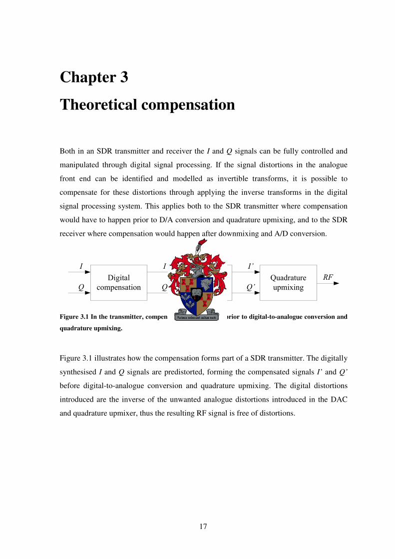
Chapter 3
Theoretical compensation
Both in an SDR transmitter and receiver the I and Q signals can be fully controlled and
manipulated through digital signal processing. If the signal distortions in the analogue
front end can be identified and modelled as invertible transforms, it is possible to
compensate for these distortions through applying the inverse transforms in the digital
signal processing system. This applies both to the SDR transmitter where compensation
would have to happen prior to D/A conversion and quadrature upmixing, and to the SDR
receiver where compensation would happen after downmixing and A/D conversion.
�������
��� ����
����������
����� ����
�
�
�
�
Figure 3.1 In the transmitter, compensation is performed prior to digital-to-analogue conversion and
quadrature upmixing.
Figure 3.1 illustrates how the compensation forms part of a SDR transmitter. The digitally
synthesised I and Q signals are predistorted, forming the compensated signals I’ and Q’
before digital-to-analogue conversion and quadrature upmixing. The digital distortions
introduced are the inverse of the unwanted analogue distortions introduced in the DAC
and quadrature upmixer, thus the resulting RF signal is free of distortions.

18
����������
�� ��� �
�������
��� ���� ���
�
�
�
�
Figure 3.2 In the receiver, compensation is performed after quadrature downmixing and analogue-to-
digital conversion.
A SDR receiver is illustrated in Figure 3.2. Here digital compensation will naturally have
to be performed after downmixing and analogue-to-digital conversion, but this is not
important. The same compensation techniques can be used both in the transmitter and in
the receiver. In the receiver compensator, the input signals I and Q will have distortions
introduced by the quadrature downmixer and the ADC. These analogue distortions are
negated through introducing inverse distortions digitally, forming the distortion free
signals I’ and Q’ which are further passed on to the demodulation process.
3.1 Compensation principles
As described in [23] it is always possible in a digital processing system to compensate for
deterministic distortion effects in the analogue front end as long as these distortions can
be modelled as a cascade of invertible transforms. The accuracy of such compensation is
only limited by the accuracy of the system’s numeric representation and the accuracy
with which the distortion effects can be measured.
���� ���������� ���������� ����
���������� �� ��� ���� ���������� ���
Figure 3.3 Compensation must be performed in reverse order.

19
Figure 3.3 illustrates how a series of invertible distortion transforms can be compensated
for through applying the inverse transforms in reverse order. This is possible if the
transforms are invertible,
{ }{ } { }{ }1 1andA A x x B B x x− −= = (3.1)
In general it is necessary to apply the inverse transforms in reverse order because it
cannot be assumed that the transforms are commutative;
{ }{ } { }{ }1 1 1 1A B x B A x− − − −≠ (3.2)
As was shown in [23], the quadrature inaccuracies described in Chapter 2.2 can be
modelled as a series of invertible transforms and hence it is possible to compensate for
them through signal processing in the digital domain.
3.2 Amplitude compensation
A mismatch in signal amplitude between the I and Q channels can be compensated for
through scaling one of the two channels with the correct factor so that amplitude balance
is restored. For example one could scale the I signal with an amplitude compensation
factor, CA, and leave the Q signal as is, the compensated signals I'(t) and Q'(t) are then
found by
( ) ( )
( ) ( )
1'
1
'A
I t I tC
Q t Q t
= ⋅+
= (3.3)
3.3 Phase compensation
Just as for amplitude deviation, the phase difference between the I and Q signals can also
be manipulated in the digital domain, although the process is slightly more complex. In
[23] two different methods for phase compensation are described, namely ‘Hilbert

20
filtering’ and ‘phasor rotation and scaling’. Here a third method is developed based on
familiar trigonometric identities.
A complex baseband signal can be defined as follows
( ) ( ) ( )( ) ( ) ( )
cos
sin
I t a t t
Q t a t t
φφ
=
= (3.4)
The I and Q signals should have a phase difference of exactly 90 degrees. If this is not the
case this could be obtained by adjusting the relative phase of the signals with a phase
compensation factor CP. The phase compensation could be divided equally between the
two channels so that the I channel is given a phase shift of / 2PC+ and the Q channel is
given a phase shift of / 2PC− ,
( ) ( )
( ) ( )
( ) ( )
( ) ( )
' cos2
cos cos sin sin2 2
' sin2
sin cos cos sin2 2
P
P P
P
P P
CI t t
C Ct t
CQ t t
C Ct t
φ
φ φ
φ
φ φ
� �= +� �
� � � �= −� � � �
� �= −� �
� � � �= −� � � �
(3.5)
In Equation (3.5) the amplitude, a(t), is left out for simplicity and the trigonometric
identities
( )( )
cos cos cos sin sin
sin sin cos cos sin
a b a b a b
a b a b a b
+ = −
− = − (3.6)
are used to expand the expressions. Substituting Equation (3.4) into Equation (3.5) gives

21
( ) ( ) ( )
( ) ( ) ( )
' cos sin2 2
' cos sin2 2
P P
P P
C CI t I t Q t
C CQ t Q t I t
� � � �= −� � � �
� � � �= −� � � �
(3.7)
which can be easily calculated in the digital domain.
p∆
Figure 3.4 Effect on signal amplitude of a phase shift, �p, in the I channel.
The phase compensation process described above scales the amplitude, a(t), of the I and
Q signals to a(t)·cos( PC ). Figure 3.4 illustrates how the amplitude of the I channel is
affected. As can be seen the resulting amplitude after compensation is
( ) ( ) ( )' cos PI t I t C= ⋅ (3.8)
Although the amplitude of the signal is not critical as long as the I and Q signals are
scaled equally as is the case here, it might be desirable to restore the signal amplitude.
This can be done by multiplying both the I and Q signals with 1/ cos PC . The final
expression for the phase compensated signals I’(t) and Q’(t) is then
( ) ( ) ( )
( ) ( ) ( )
1' cos sin
cos 2 2
1' cos sin
cos 2 2
P P
P
P P
P
C CI t I t Q t
C
C CQ t I t I t
C
� �� � � �= −� � � �� � � �
� �� � � �= −� � � �� � � �
(3.9)

22
3.4 DC compensation
A DC offset can be removed simply by subtracting the I and Q components of the offset
from the I and Q channels respectively. Denoting the I component of the DC offset Ci and
the Q component Cq, the compensated signals I’(t) and Q’(t) are found by
( ) ( )( ) ( )
'
'i
q
I t I t C
Q t Q t C
= −
= − (3.10)
There is no limitation on the DC offset that can be compensated digitally. However, it is
worth noting that a large DC offset in a receiver effectively reduces the dynamic range of
the ADC. It is therefore desirable to minimise the DC offset as much as possible through
analogue design in order not to degrade the noise figure of the receiver.
In this chapter, principles for compensation have been described. It has been illustrated
how deliberate amplitude deviation, phase error and DC offset can be introduced to the
baseband signal. The hardware errors in the transmitter and receiver can be modelled as
reversible transforms. If the values of the hardware errors can be found, then the
described compensation techniques can be used to cancel the effects of the errors through
introducing the inverse transforms in the digital domain.

23
Chapter 4
Automatic calibration
It was shown in Chapter 3 that it is possible to negate the effects of quadrature errors
through compensation in the digital domain once one knows the compensation factors:
Amplitude deviation compensation factor CA
Phase error compensation factor CP
I channel DC offset compensation factor Ci
Q channel DC offset compensation factor Cq
In this chapter, calibration methods for both a transmitter and a receiver are proposed.
This is the main contribution of the thesis. It is shown how the compensation factors can
be detected through exploiting the relationship between the quadrature errors and their
effect on the frequency spectrum. As described in Chapter 2.2, quadrature errors in a
quadrature mixer produce unwanted spurs in the frequency spectrum when the input is a
single tone. This property applies in the same way to both a quadrature upmixer and a
downmixer, and it can be exploited to make a calibration system where the compensation
factors are automatically detected.
The proposed calibration approach is not limited to one specific modulation scheme.
After calibration, all the hardware imperfections in the transmitter and receiver are
compensated for. The compensators in the transmitter and the receiver forms part of the
RF-link layer together with quadrature mixing RF front end. The modulator and
demodulator see the RF front end together with the compensator as one perfect frequency
conversion stage.

24
Figure 4.1 Quadrature mixing receiver with calibrator. During calibration, the RF input must be a
single tone close to the carrier frequency. The calibrator detects the compensation factors, which are
stored in the compensator.
A schematic diagram of a quadrature-mixing receiver is shown in Figure 4.1. As
described in Chapter 2.2, the quadrature errors can originate from the quadrature mixer
itself, from the low-pass filters or from the ADCs. The combined errors can be
compensated by digital manipulation of the complex baseband signal after downmixing
but prior to demodulation. The calibration system in Figure 4.1 functions like a feedback
loop. The input signal during calibration has to be a single frequency close to the
downmixing carrier frequency. The calibrator uses an FFT to analyse the I and Q signals
in the frequency domain. The sideband and DC spurs originating from quadrature errors
are identified and measured, and based on these measurements compensation factors are
calculated and passed on to the compensator. For receiver calibration, measurements are
done on a complex signal, making it possible to determine both the magnitude and the
phase of the sideband and DC spurs. This makes it possible to calculate the optimum
compensation factors directly in one operation, however a number of factors that will be
discussed later can make it necessary to perform calibration in multiple iterations. After
calibration, the calibrator can be disconnected from the system, which resumes normal
operation.

25
Figure 4.2 Transmitter calibration
Figure 4.2 shows a similar calibration system for a quadrature mixing transmitter. As seen
in Figure 4.1 the feedback loop performing receiver calibration is made up of only the
compensator and the calibrator, both of which can be implemented in the same digital
system. The transmitter calibration feedback loop however, is a bit more complex. While
the measurements needed for receiver calibration are done on a baseband signal in the
digital domain, the measurements for transmitter calibration must be done on an analogue
RF signal at the carrier frequency. These measurements will then have to be converted to
the digital domain where compensation is to take place. One way to do this is to use a
spectrum analyser with an interface to the digital compensation system. Another solution
to the problem is to use a quadrature mixing receiver in the feedback loop. This approach
has a number of appealing attributes: It converts the signal to a digital complex baseband
signal so that the same digital FFT used for receiver calibration can also be used for
transmitter calibration. A quadrature mixing receiver is a much smaller and less
expensive device than a spectrum analyser, and although this might not be of major
importance in a factory calibration system, it opens up the interesting opportunity of
performing calibration in the field. The receiver must of course be calibrated before it can
be used for transmitter calibration, otherwise it would introduce additional quadrature
errors. A transceiver that uses quadrature mixing both in its transmitter and receiver
stages can, with very little extra hardware, be designed to calibrate itself whenever it is
required. Such a self-calibrating transceiver design is described in Chapter 4.4.
Transmitter calibration with a quadrature downmixer in the feedback loop becomes even
more elegant if the upmixer and downmixer can share their local oscillators so that
coherent downmixing is taking place. In that case, the calibrator can measure the phase of
26
the sideband and carrier spurs and use this information to calculate the compensation
factors directly. When coherent downmixing cannot be performed, or when using a
spectrum analyser to measure the spectrum, only the magnitude of the spur can be
measured, which necessitates use of an iterative calibration algorithm.
As mentioned the suggested calibration approach is based on inputting a constant
frequency signal as a test signal to the quadrature mixer. In the following discussion, this
signal will be referred to as the calibration frequency, fcal. For a transmitter the input
during calibration is simply fcal, while for a receiver the input is fc + fcal, where fc is the
carrier frequency. The only requirement for fcal is that it produces a measurable spur in the
frequency spectrum. This means it must be below half the sampling frequency and it must
not be so close to 0 Hz that it interferes with a centre spur. The latter depends on the
number of samples, N, used for the Fourier transform and the sampling frequency as well
as the choice of windowing function. This will be discussed in Chapter 4.3. The
calibration frequency can be negative. Several methods of detecting the compensation
factors from the effects on the test signal were examined:
• Linear search / interval halving
• Gradient search
• Direct calculation
• Fast iterative
• Averaging DC
All except the averaging DC method are based on analysing the quadrature mixer’s
output in the frequency domain. All the calibration methods analyse the centre and
sideband spurs independently so that amplitude and phase calibration is one process and
DC calibration another process. Generally the amplitude and phase errors should be found
and compensated prior to DC calibration since the phase error also has an effect on the
DC spur.

27
4.1 Calibration with phase information;
the direct calculation method
When it is possible to measure both the magnitude and the phase of the carrier and
sideband spurs, the compensation factors can be calculated directly. This is the fastest
method and under ideal circumstances, it only requires two spectral measurements to be
performed. First, the sideband spur is measured, and the amplitude and phase errors are
compensated. Then the carrier spur is measured in a new measurement and the DC error
is compensated. As described in Chapter 2.2.2 the phase error is assumed to be small. If
this is not the case, or if the measurements are noisy, it might be necessary to perform
multiple iterations of the algorithm depending on the desired accuracy of the calibration
outcome. When multiple iterations are performed, the algorithm will converge towards
the correct values for the compensation factors.
4.1.1 Calibration of amplitude deviation and phase error
As shown in Chapters 2.2.1 and 2.2.2, both amplitude deviation and phase error produces
a sideband spur. For small phase errors, their contributions to the spur will be orthogonal
so that the resulting sideband spur will be
,bsS S jSρ κθ∠ = + (4.1)
where Sbs is the magnitude of the spur, and � is the spur phase relative to the phase of the
desired signal. The fact that the contributions are orthogonal is important, because it
allows the individual contributions to be found by simple vector decomposition. The
amplitude deviation component is found by
( )cosbsS Sρ θ= (4.2)
and the phase error component;
( )sinbsS Sκ θ= (4.3)

28
Finding the amplitude compensation factor
From Equation (2.11), it follows that the amplitude deviation, �, can be found by
2
1
S
Sρ
ρ
ρ =−
(4.4)
Now that the amplitude deviation, �, is found, it can be used as CA in Equation (3.3) to
compensate for the amplitude deviation.
Finding the phase compensation factor
From Equation (2.13) it follows that the phase error, �, can be found by
2
2
1
S
Sκ
κ
κ =−
(4.5)
The phase error can be used directly as PC in Equation (3.9) to compensate for the phase
error.
4.1.2 Calibration of DC offset
If the magnitude of the carrier spur is �, and the spur phase �, then the DC compensation
factors Ci and Cq are found by
( )( )
cos
sini
q
C
C
α γα γ
=
= (4.6)
The DC compensation factors can be used with Equation (3.10) to perform DC
compensation.

29
4.1.3 Algorithm
The following pseudo code describes a calibration algorithm using the methods for
directly calculating the compensation factors as described above:
if (sideband_mag > tolerance) � = sideband_phase + signal_phase Sk = sideband_mag * sin(�) Sp = sideband_mag * cos(�) Rho = 2*Sp / 1-Sp CA = CA + Rho Kappa = 2 * Sk / sqrt(1-Sk2) CP = CP + Kappa else if (dc_mag > tolerance) dci_inc = centre_mag * cos(dc_phase) dcq_inc = centre_mag * sin(dc_phase) Ci = Ci + dci_inc Cq = Cq + dcq_inc end
Figure 4.3 Pseudo code describing the direct calculation method.
The compensation factors are all incremented rather than replaced with new values,
allowing the calibration routine to converge towards a better solution if necessary.
Whenever a recalibration is performed, it is a good idea to start with the compensation
factors from last calibration since that will normally provide a starting point closer to the
optimum solution than assuming there are no errors and setting all compensation factors
to zero. As specified by the else statement, dc compensation is only performed once
amplitude and phase compensation is done.
4.2 Calibration without phase information
It is not always possible to measure the phase of the carrier and sideband spurs. This will
most often be the case when performing transmitter calibration, except when a receiver
with coherent downmixing is used in the feedback loop. Two different algorithms to
handle calibration without phase information are proposed. The fast iterative algorithm is
the faster of the two. It does require knowledge about the amplitude of signal that’s being
compensated in order to be able to perform DC calibration. The gradient search method
can be used even when the amplitude of the signal is unknown.

30
4.2.1 The fast iterative method
The fast iterative algorithm is similar to the direct calculation but rather than measuring
the phase directly from the spectrum, it is able to assess it through doing three or four
measurements. The algorithm is described by the pseudo code of Figure 4.4.
if (sideband_mag > tolerance) A = sideband_mag � = 0 Calculate CA and CP as in Figure 4.3, mag A, angle � B = sideband_mag � = 2 * asin((B / A) / 2) Calculate CA and CP as in Figure 4.3, mag A, angle � C = sideband_mag if (C < B and C < A) Compensation is achieved else � = -� Calculate CA and CP as in Figure 4.3, mag A, angle � Now compensation is achieved else if (dc_mag > tolerance) A = centre_mag � = 0 Calculate Ci and Cq as in Figure 4.3, mag A, angle � B = centre_mag � = 2 * asin((B / A) / 2) Calculate Ci and Cq as in Figure 4.3, mag A, angle � C = centre_mag if (C < B and C < A) Compensation is achieved else � = -� Calculate Ci and Cq as in Figure 4.3, mag A, angle � Now compensation is achieved end
Figure 4.4 Pseudo code describing the fast iterative calibration method.
On the first iteration, the spur magnitude is measured and stored in the variable A, and the
compensation factors are calculated with the phase set to zero. For amplitude and phase
compensation, this means it is assumed the total sideband spur is caused by amplitude
deviation only, and for DC compensation it is assumed there is only DC offset in the I
channel. After making this adjustment, the spur magnitude is measured again as B, and
now the angle, �, can be found by
2arcsin2
B Aθ � �= ± � �
(4.7)

31
as described in [23]. As only the absolute value and not the sign of the phase angle is
found, it is first assumed to be positive and a third measurement must be performed to
verify if the assumption was correct. If the spur magnitude in this third measurement is
smaller than both the two initial measurements, the correct angle has been found and the
routine is finished. If the spur magnitude in the third measurement is larger, then the sign
of the angle, �, is changed, and a fourth measurement is performed. This last
measurement is only necessary to verify if the calibration has succeeded in bringing the
spur magnitude to below the set tolerance. If this has been achieved then the calibration is
finished, otherwise the entire procedure is repeated.
As mentioned this calibration method only needs to measure the magnitudes of the spurs
and not the phase, which makes it a good choice for transmitter calibration with non-
coherent downmixing. It is important to note that the magnitude of the sideband spur is
measured relative to the signal’s magnitude, while for the DC spur the absolute
magnitude needs to be measured without any reference. For transmitter calibration there
will be a, normally unknown, gain or attenuation between the baseband signal at the
transmitter side and the signal at the receiver side. The DC spur can be normalised
relative to the signal amplitude on the receiver side. The calculated dc compensation
factors will then be relative to the signal amplitude. They must then be scaled with the
signal amplitude on the transmitter side to give the correct compensation factors.
4.2.2 The gradient search method
This method uses a relatively simple gradient search algorithm to find the optimal
compensation factors. The algorithm is based on the method of steepest descent
[9][25][26], however the implementation differs slightly. This method was used to
investigate the problem during the initial stages of the project. The performance of this
method could have been improved through further optimisation. However, it was chosen
rather to focus the optimisation efforts on the direct calculation method, described in
Chapter 4.1, and the fast iterative method, described in Chapter 4.2.1.
The search space for the DC spur is shown in Figure 4.5, and the optimal compensation
factors, Ci and Cq, are found at the minimum of the surface. As can be seen, the surface
has the shape of a slightly oval cone. The oval shape is caused by phase offset.

32
Figure 4.5 Magnitude of centre frequency spur with a DC offset of 0.1+0.1j and Phase error of 0.3 rad.
In order to determine the gradient of the surface, the algorithm does three measurements,
between which the compensation factors Ci and Cq, are adjusted by a step size, s, as
illustrated in Figure 4.6.
Figure 4.6 Three measurements, A, B and C, are made to determine the direction of the next jump.

33
As described in [9] the method of steepest descent will approach the minimum of the
surface in a zigzag pattern, with each new search direction being orthogonal to the
previous. For this reason, it was chosen to let the algorithm only perform jumps in the
directions of the I and the Q axes, as that simplifies the implementation. Figure 4.7
illustrates how the algorithm performs DC calibration. Amplitude and phase
compensation would be performed in exactly the same way, with Ci and Cq replaced with
CA and CP.
while (spur magnitude > tolerance) A = spur magnitude Ci = Ci + s B = spur magnitude Ci = Ci – s Cq = Cq + s C = spur magnitude Cq = Cq – s if (|A-B| > |A-C|) //Make a change to Ci if (A > B) //Increase Ci M = (A + B) / 2 Ci = Ci + M
PD else if (A < B)//Decrease Ci M = (A + B) / 2 Ci = Ci – M
PD else if (|A-B| < |A-C|) //Make a change to Cq if (A > C) //Increase Cq M = (A + C) / 2 Cq = Cq + M
PD else if (A < C)//Decrease Cq M = (A + C) / 2 Cq = Cq – M
PD end
Figure 4.7 Pseudo code for the gradient search calibration method.
The algorithm first performs the three magnitude measurements A, B and C, as illustrated
in Figure 4.6. When the measurements are done it checks if the gradient is steeper in the I
or the Q direction and whether the gradient is positive or negative. The direction of the
next jump is now found. The length of the jump, �dc, is calculated based on the
remaining spur magnitude, which is scaled with a proportional factor, D, and an
exponential factor, P;
P
dc dcmag D∆ = ⋅ (4.8)

34
The variable dcmag in Equation (4.8) is the spur magnitude, which is approximated
simply by averaging the two relevant measurements. The gradient of the surface is not
actually calculated because it is constant, as can be seen in Figure 4.5, and so it does not
hold any information about how far away the minimum is.
The gradient search algorithm continuously adjusts the compensation factors in small
steps, s, in order to measure the gradient of the search space. For this reason the exact
value of the compensation factors will never be found, but rather than this the algorithm
converges to a state where the steps, s, will jump back and forth over the correct value.
This means that with this method there will always be a residual error of 2s
. The
maximum step size, s, can be expressed in terms of the desired spurious free dynamic
range, SFDR, as
2020SFDR
s = (4.9)
The exponential factor, P, in Equation (4.8) ensures that the jumps are exponentially
dampened as dcmag becomes smaller. A value of 1.2 for P has been found to work well.
The factor, D, is a proportional dampening factor. When compensation is performed on
the same signal that is being measured, as is the case for receiver calibration, D should be
set to 1. If there is a gain between the compensator and the measured signal, as will often
be the case when transmitter calibration is performed, this factor should be adjusted to
compensate for the gain. The algorithm will converge towards the correct value even
when D does not accurately represent the gain, unless D is too big in which case the
algorithm will become unstable and oscillate around the solution. This means that this
algorithm will function for transmitter calibration even when the gain between the
transmitter and the receiver is unknown. It will however converge slower when the gain is
not well estimated.
4.2.3 Averaging DC
An alternative approach to determining the DC calibration factors is to measure the
average of the I and Q channels in the time domain. Since the test signal is a sine that is

35
symmetrical around 0, the measured average value will be the DC offset. To give an
accurate result the signal must however be measured over a period that corresponds to an
exact multiple of the signal period. One drawback with this method is that it does not
have the ability to converge towards the correct value if the first compensator factor
estimate is inaccurate, like the methods performing measurements in the frequency
domain do.
4.3 Implementation considerations
In the previous two chapters, ways to find the compensation factors from measurements
of the magnitude and phase or magnitude alone of the sideband and DC spurs. In this
chapter, the problems of locating the spurs in the spectrum and measuring them with the
required accuracy will be addressed.
4.3.1 Spur detection
In order to be able to measure the DC and sideband spurs, their position in the frequency
spectrum must first be determined. If the exact frequency of the calibration signal, fcal, is
known, its position in the FFT spectrum is given by the bin number, n, which can simply
be calculated by
round ,cal
s
f Nn
f� �⋅= � �
(4.10)
where N is the total number of FFT bins and fs is the sampling frequency, and n is
rounded to the nearest integer. The DC spur will always be found at 0 Hz when
performing transmitter calibration and when performing transmitter calibration with a
coherent downmixer. When performing transmitter calibration with non-coherent
downmixing the entire frequency spectrum is shifted with a frequency
.shift upmixer downmixerf f f= − (4.11)

36
The position of the signal spur can then be found by substituting fshift + fcal for fcal in
Equation (4.10), and the position of the DC spur is found by substituting fshift for fcal in
Equation (4.10). When the signal and DC spurs are found, the sideband spur can always
be found as the reflection of the signal spur around the DC spur.
In some cases it might be impractical to have to tell the calibration system what
calibration frequency is being used for it to detect the spurs. For example when
performing calibration at multiple frequencies it would be useful if the calibrator could
automatically detect the frequency of the input signal. It could also be that the frequency
of the calibration signal is not known exactly. This does not affect the calibration as the
only requirements for the calibration signal are that it is a single frequency within the
band for which the quadrature mixer is to be calibrated, and that it is sufficiently far away
from the carrier frequency for the two frequency spurs to be measured without interfering
with each other. The latter depends on the FFT size, N, and the sampling frequency, fc, as
these two parameters determine the “frequency resolution of the spectrum”. Often the
signal spur will be the largest spur in the spectrum, in which case it can be detected
simply by searching the entire spectrum for the largest spur. However, it is not always
safe to assume that the signal spur is the largest, as a strong DC offset may produce an
even larger spur. It might therefore be useful to ignore the bins around 0 Hz when
searching the spectrum for the signal spur.
4.3.2 Spectral measurement
In order to be able to calculate the compensation factors, the magnitude of the sideband
and centre spurs must be measured as well as the signal itself. In order to be able to use
the direct calculation method, which is the fastest of the calibration methods described
here, the phase of all three spurs must also be measured. The accuracy with which the
measurements can be made determines how accurately the compensation factors can be
found. The Discrete Fourier Transform (DFT) is the maximum likelihood estimator for
amplitude and phase [8], thus it is the preferred method for spur measurement. The DFT
can be calculated as [3]
( ) ( )21
0
0,1,..., 1mnN j
N
n
X m x n e m Nπ− −
=
= = − (4.12)
37
where X(m) is the DFT of a series of N samples of the signal x(n). The Fast Fourier
Transform (FFT) is an efficient implementation of the DFT suitable for computer
applications. For that reason, the FFT was chosen to perform the spectral measurements
required for the calibration.
Windowing
The frequency of the spur to be measured will normally not be an exact multiple of the
FFT’s frequency spacing. This is the reason why the rounding function is needed in
Equation (4.10). When the frequency of the spur is not precisely at the centre of a bin,
spectral leakage will occur. The energy of the signal is not contained in one bin alone, but
spread over a number of bins, so that there is no single bin representing the amplitude of
the signal correctly. A way to get a better estimate of the signals amplitude than just to
look at the closest FFT bin would be to sum the values of this bin and a number of
neighbouring bins. A more sophisticated way is to use a windowing function prior to
performing the FFT.
A Blackman window was found to be a good choice for this application based
comparisons of several windows from [7] and [13]. It guarantees a fairly accurate
amplitude measurement, even when the frequency of the spur lands midway between two
FFT bins, which is the worst case scenario. A Flat-Top window would do this job even
better, and always give an entirely accurate amplitude measurement. However, the
Blackman window has another important property in that it has a good low-level limit,
which means that it allows measurement of small signals in the presence of large signals.
This is important since it must be possible to measure the unwanted DC and sideband
spurs even when they are very small compared to the desired signal. Choosing the right
window is a bit of a trade-off, and one drawback with the Blackman window is that it has
a wide peak, thus it is not able to resolve signals very close in frequency. This is however
not critical to this application, as it can be dealt with by choosing a calibration frequency
sufficiently far away from the carrier frequency.
The windowing leads to a loss in the total power in the FFT. A way to negate this is to
normalise the FFT by dividing each FFT sample, X(m), with the sum of all the window

38
samples. After normalising the correct spur magnitudes can be read directly from the
spectrum. An unwindowed FFT could be normalised by dividing with N, which is the
sum of a square window.
Accuracy and FFT size
The accuracy of the proposed calibration method is only limited by the accuracy with
which the spurs can be measured and how accurately the compensation factors can be
represented. The latter depends on the numeric representation of the compensation system
and imposes an absolute boundary. The former depends on the noise in the system and the
FFT size, which is a design choice. The calibration can suppress the unwanted spurs to
the level where they can no longer be measured, i.e. to the point where they disappear in
the noise floor. Through increasing the number of samples, N, used to calculate the FFT,
the processing gain of the system is increased, so that any spurious component can be
measured if only N is large enough. The processing gain of the FFT increases with 6 dB
each time N is doubled. The test signal is only given a gain because it is periodic through
the entire FFT frame. Noise does not have any periodic properties, thus it is not subject to
a processing gain. The same is true for any information-bearing signal. Such a signal
would necessarily have to be time variant, so just like the noise it is not subject to a
processing gain. For this reason, the noise floor imposes an absolute limit on the dynamic
range of an information-bearing signal. Therefore, compensating beyond the noise floor
of the system does not really have any practical value.
In a digital system, there will be a quantisation noise, which depends on the number of
levels used for signal representation and the compression used in the system. For a linear
system with a resolution of b bits, the signal to noise ratio in decibels caused by the
quantisation noise is [17]
6.02 dBqSNR b= ⋅ . (4.13)
If compression such as A-law or �-law is used, then the expression becomes different
however, this is described in detail in [17]. In a calibration system, care should be taken
to minimise the thermal noise, in which case the noise floor can be expected to be caused
39
by the quantisation noise. The calibration signal is a sine, and for a sine wave the
expected SNR is
1.76 6.02 dBqSNR b= + ⋅ . (4.14)
This expresses the ratio between a power of a sine wave of maximum amplitude i.e. that
goes through all quantisation levels, and the power of the noise floor caused by quantising
the sine with b bits resolution.
Equation (4.14) gives a power ratio which can not be related directly to the noise floor as
seen in the FFT. The noise power given by Equation (4.14) does however correspond
with the noise floor in a power density spectrum (PDS) [11]. The PDS, S(m), can be
calculated as
( ) ( ) 21S m X m
N= (4.15)
where X(m) is the FFT of length N. While the PDS represents the noise floor correctly, it
introduces a processing gain of 2N for a sine component. In order to be able to measure
a signal, the signal spur must appear above this level in the PDS. The last element to take
into account is the loss caused by the window function. The loss for a Blackman window
is 7.569 dB [7]. Now it is possible to calculate how many points, N, that must be used to
calculate the PDS in order to make a spurious component of a certain power appear above
the noise floor.
An example SDR could have a quantiser with a resolution of 14 bits and a design goal to
suppress the spurs to −100 dBW. Equation (4.14) predicts that the PDS noise floor in this
case will be found at −86 dB. The number of points, N, must be selected so that it gives a
processing gain that lifts the −100 dBW signal above the −86 dB noise floor. The
processing gain must then be −100 dBW + 7.569 dB − 86 dB = 21.569 dB. For a 1024 pt
PDS the processing gain is

40
1024
10 log 27.1 dB2
� �⋅ =� �
(4.16)
which is sufficient to lift the spur above the noise floor. Figure 4.8 shows a simulation
result for the example.
0 50 100 150 200 250 300 350 400 450 500−120
−100
−80
−60
−40
−20
0
20
Frequency [samples]
Mag
nitu
de [d
BW
]
Figure 4.8 1024 pt PDS of two sine waves. The power of the large signal at sample 47 is measured to
16.5 dBW. When corrected for processing gain the power correctly becomes −3 dBW. The second
signal at sample 313 has a measured power of −80.5 dBW. The corrected power for this signal is −100
dBW.
The large spur at sample 47 has an amplitude of 1. The power of a sine with amplitude A
is
2
10log dBW2A
P� �
= � �
, (4.17)

41
which gives a power of –3 dBW for the sine. With the processing gain and the window
loss it is correctly displayed at 16.5 dBW in the PDS. The small spur at sample 313 is a
sine with amplitude 1.4·10-5, which corresponds to a power of −100 dBW. It was
predicted that the noise floor due to the 14 bit quantisation would be found at −86 dBW
and that the −100 dBW spur would stand out ca 5.5 dB above the noise floor. As can be
seen from Figure 4.8 the simulation results confirm the predictions. The simulation also
confirms that it is possible to measure a small signal in presence of a much larger one
with a Blackman window.
A PDS was used as basis for the discussion here because the noise floor in the PDS
corresponds with the quantisation noise power predicted by Equation (4.14). The results
are however also applicable for an FFT. In an FFT that is normalised by dividing with the
sum of the window, the correct amplitude of the spurs is measured independently of the
FFT size, N. Here the processing gain from increasing N can be seen as pushing the noise
floor in the spectrum down, rather than increasing the magnitude of the spurs.
4.4 Proposed architecture – the self calibrating transceiver
The quadrature errors are dependent on operating frequency and temperature. Factory
calibration can take the frequency dependent variation into account through calibrating at
a number of frequencies and storing the compensation factors in the device. As a goal for
a software radio is that it should be totally flexible and able to operate in any frequency
band, a large amount of calibration data would have to be stored in order to ensure
optimal performance at all frequencies. To deal with the temperature dependent variation
through factory calibration would normally be impractical since that would mean the
device would need a temperature sensor built in order to know what compensation data to
use. As mentioned in the introduction to this chapter, using a quadrature downmixer in
the feedback loop for transmitter calibration opens up the possibility of making a self
calibrating transceiver. With the calibration approaches developed in this thesis,
calibration can be done in only a few seconds. It could then be natural to allow the
transceiver to perform self-calibration routine on power on and each time transmission
mode or carrier frequency is changed. This would greatly reduce the memory needed for

42
storing calibration data. The temperature factor would also to some extent be dealt with in
that the transceiver calibrates itself within its current operating environment.
A schematic diagram of a self-calibrating transceiver is shown in Figure 4.9. The
compensation and calibration is taking place in software along with modulation and
demodulation. The only extra hardware requirement is one extra variable oscillator as a
calibration reference for the receiver.
Figure 4.9 Schematic diagram of a self calibrating transceiver.
Both compensators have a memory where compensation factors are stored after
calibration.
In normal operational mode, the calibrator is disconnected and both the transmitter and
the receiver are connected to the antenna. The transceiver can be calibrated through the
following steps:
1. First the receiver side is calibrated using an external signal source as a reference.
The Quadrature downmixer is connected to the signal source, the receiver
compensator output is connected to the calibrator input and the calibrator output is
connected to the receiver compensator input.
2. The signal source generates a single tone within the frequency band the system is
to be calibrated for.

43
3. The calibrator detects the optimal compensation factors for the receiver. These
compensation factors are stored in the receiver compensator. The receiver is now
calibrated.
4. Secondly the transmitter is calibrated using the calibrated receiver as part of the
feedback loop. The calibrator output is connected to the transmitter compensator.
The quadrature upmixer is connected directly to the downmixer and the antenna is
disconnected.
5. The modulator is set to modulate a constant value i.e. transmit a single tone.
6. The calibrator finds the optimal compensation factors for the transmitter. These
compensation factors are stored in the transmitter compensator.
7. The system is now calibrated and returns to normal operational mode.
With this architecture, the transceiver can calibrate itself in the field whenever it is
required. No transmission is being done with an uncalibrated transmitter, so there is no
danger of interference to neighbouring channels.
4.5 Conclusion
In this chapter, an automated calibration method to carry out calibration of a QM
transmitter and receiver has been developed. Several calibration algorithms has been
proposed. For receiver calibration and transmitter calibration with coherent downmixing
of the RF spectrum, the direct calculation algorithm is generally the fastest. For
transmitter calibration when coherent downmixing of the RF spectrum is not possible,
two FFT based algorithms were proposed, as well as the simpler method of calculating
the DC offset through averaging in the time domain. It was shown in Chapter 4.3.2 that
the calibration accuracy is only limited by the accuracy of the numeric representation of
the compensation system. Finally, a complete design for a self-calibrating SDR
transceiver has been suggested.
The developed calibration method and all the described algorithms were implemented and
tested both in Matlab Simulink simulations and in a real PC based SDR system with QM
front end. In the following chapter, the simulations are described, while the real
implementation is described in Chapter 6.

44
Chapter 5
Simulations
Throughout the project, Matlab Simulink has been used to test all ideas, and aid the
development process. All the calibration methods described in Chapter 4 have been
implemented and tested in Simulink models. Three models of full SDR systems have
been developed, with calibration based on the calibration methods; direct calculation, fast
iterative and gradient search. A quadrature mixing blockset for Simulink has also been
developed. The blockset contains quadrature mixers, compensators and calibrators
implementing the different calibration algorithms. The transceiver system models and the
quadrature mixing blockset are included on the attached CD, and the reader is encouraged
to have a look at the models as they illustrate the presented calibration principles very
well.
In this chapter, one of the developed models will be described in detail in order to present
the work that has been done in Simulink. This model also presents a different approach to
calibration than the self-calibrating transceiver system described in Chapter 4.4. The
calibration approach here can be used in a non-duplex system, where both the transmitter
and the receiver are equipped with their own calibrators. In the transmitter, calibration
measurements are done in the RF spectrum, as can be done with a spectrum analyser. FM
is used in this simulation, but as mentioned, the calibration is independent of the
modulation scheme, so any modulation scheme could have been used. The model uses the
gradient search algorithm to perform both transmitter and receiver calibration.

45
5.1 General description of the model
An SDR communications link, consisting of self calibrating transmitter and receivers is
illustrated in Figure 5.1. The transmission side consists of the input signal, which is fed
into the Baseband Compensating FM Modulator, which performs FM modulation and
phase compensation. The modulated FM signal is then fed into the Transmitter
Compensator, which performs compensation for DC offset and amplitude deviation. The
modulated and predistorted signal is then upmixed to carrier frequency by the Quadrature
Upmixer. The RF signal is fed back to the Transmitter Calibrator, which finds the
compensation factors used in the compensator blocks. The calibrator works in close
connection to the compensator block. However, the two blocks are kept separate so that
the calibrator can easily be replaced with a different calibrator implementing another
calibration algorithm. The calibrator can also be disabled after the compensation factors
have been found.
Figure 5.1 Simulink model of SDR system with individually calibrated transmitter and receiver.

46
At the receiver side, the transmitted signal is downmixed from RF to baseband by the
Quadrature Downmixer, before it is passed through the Receiver Compensator which
compensates for the inaccuracies in the downmixer. In the same manner as on the
transmitter side, the compensation factors used by the Receiver Compensator are
calculated by the Receiver calibrator. After compensation, the signal is demodulated by
the Baseband FM Demodulator. Finally, the demodulated signal is displayed on an
oscilloscope together with the original input signal to the transmitter.
The simulation window also contains a block for setting parameters for the calibrators,
two blocks for enabling or disabling various oscilloscopes and a Compensator Memory
Bank. The memory bank holds the values for the different compensator factors. These
values are written by the calibrator blocks and read by the compensator blocks, thus the
memory bank acts as the link between the two blocks and it needs to be visible on the top
level of the simulation to be accessible to both the blocks. The two scope blocks allow the
viewer of the simulation to switch on and off a range of scopes for the model. The
calibrator parameter settings allow changing several parameters affecting the calibrators
accuracy and speed. These parameters will be explained under the chapter about the
calibrators.
5.2 FM modulator and demodulator
The FM modulator and demodulator are taken from Simulink’s communication blockset.
The demodulator is used exactly as is, while the modulator has been modified to perform
phase compensation in the modulation process. Integrating the phase compensation with
the modulation process reduces the number of computations needed and thus makes the
design more efficient. With Simulink’s modular design it is easy to replace the modulator
and demodulator to implement another modulation scheme, illustrating how quadrature
mixing is independent of the modulation process. However, if the modulator block is
changed then phase compensation should also be performed in the compensator block.

47
5.3 The up and downmixers
Upmixing from baseband to RF on the transmitter side and downmixing from RF to
baseband at the receiver side is performed by a Quadrature upmixer and a Quadrature
downmixer block respectively. These blocks simulate the DC offset, phase error and
amplitude error as described in Chapter 2. The different errors can be set independently,
and they can even be changed during the simulation.
5.3.1 The upmixer
The quadrature upmixer takes a complex valued baseband signal and converts it to a real
valued RF signal at the desired carrier frequency.
Figure 5.2 Simulink implementation of quadrature upmixer.
The Simulink implementation of the quadrature upmixer is shown in Figure 5.2. It
simulates the upmixing process with the imperfections described in Chapter 2. The
variable “dcoff” is a complex number representing the DC offset or carrier leakthrough. It
consists of a real part iε , and an imaginary part qε which are added to the real and
imaginary parts of the baseband signal respectively. After the baseband signal is split into
its real and imaginary components, amplitude deviation, �, is applied to the two
components independently. The real part of the signal is multiplied with � while the
imaginary part is multiplied with 22 ρ− as this can be shown to maintain constant
signal energy. The real and imaginary part of the signal is then mixed with the cosine and

48
the sine of the carrier frequency respectively. The phase offset, �, is divided equally
among the cosine and the sine part of the carrier so that the resulting mixing frequencies
are ( )cos 2ctω λ− and ( )sin 2ctω λ+ . The resulting RF signal, y(t), is described by Eq.
(5.1), where I(t) and Q(t) denotes the real and imaginary part of the complex baseband
signal.
( ) ( )2( ) ( ) cos 2 ( ) sin2 2i c q cy t I t t Q t tλ λρ ε ω ρ ε ω� � � �= + − − − + +� � � �
(5.1)
The inaccuracies can be set through the subsystems mask along with the desired carrier
frequency and the sample time of the carrier. The mask is shown in Figure 5.3.
Figure 5.3 Quadrature upmixer mask with parameter settings.
5.3.2 The downmixer
The quadrature downmixer takes a real-valued modulated signal and converts it to a
complex baseband signal. Like the upmixer, the downmixer also simulates the
inaccuracies caused by hardware imperfections. The Simulink downmixer structure is
shown in Figure 5.4.

49
Figure 5.4 Simulink implementation of quadrature downmixer with carrier leakthrough, phase error
and amplitude deviation.
Firstly, a sine simulating a local oscillator leakthrough is added to the input signal. This
LO leakthrough could result from the receiver’s quadrature mixer coupling with the
received signal. It induces a DC offset in the receiver I and Q signals, and produces a
spurious component at the centre frequency. An indistinguishable spurious component
would be produced by DC offset in the I and Q channels caused by for example ADC
offset error. The LO leakthrough is a complex value, je γα , represented by the variable
recdcerr. Naming the input RF signal f(t), the RF signal after introduction of LO
leakthrough, '( )f t , is
( )'( ) ( ) cos cf t f t tα ω γ= + + (5.2)
Following the introduction of the LO leakthrough, the signal is split into two branches
where one is mixed with a cosine of the carrier frequency to form the real part of the
baseband signal, and the other is mixed with a sine of the carrier frequency to form the
imaginary part of the baseband signal. Like the upmixer, the downmixer is also capable of
simulating a phase error, �, between the sine and the cosine, and the error is divided
equally among the I and Q channels.

50
The last inaccuracy, the amplitude deviation, �, is introduced by multiplying the branch
that is to form the real part of the signal with � and the imaginary part with 22 ρ− , as in
the upmixer. Thereafter both signal paths are low-pass filtered to remove the double
frequency component resulting from the mixing. Finally the complex signal is assembled.
The gain factor of 2 is introduced simply for mathematical convenience. The resulting
complex baseband signal s(t) is given by:
2
LPF
( ) 2 '( ) cos 2 '( )sin2 2c cs t f t t j f t tλ λρ ω ρ ω� �� � � �= − − − +� � � �� �
� � (5.3)
where [ ]LPF⋅ denotes low-pass filtering and '( )f t is the received RF signal with DC offset.
As for the upmixer all inaccuracies along with the carrier frequency and sample time can
be set through the subsystem’s mask. The mask is shown in Figure 5.5.
Figure 5.5 Quadrature downmixer mask with parameter settings.

51
5.4 The compensator blocks
The model contains two compensator blocks, one in the transmitter and one in the
receiver. These blocks implement the compensation principles described in Chapter 3.
They manipulate the baseband signal to compensate for the inaccuracies of the quadrature
upmixer and downmixer.
5.4.1 Transmitter compensator and compensating FM modulator
The transmitter compensator, illustrated in Figure 5.6, only handles compensation of DC
offset and amplitude deviation. Compensation for the phase error is done in the FM
modulator block as part of the modulation process. In these two blocks deliberate DC
offset and amplitude deviation and phase error are introduced to the baseband signal in
order to compensate for the inaccuracies in the quadrature upmixer.
Figure 5.6 The transmitter compensator compensates for amplitude deviation and DC offset.
Figure 5.7 shows the phase compensating FM modulator. Since frequency modulation
controls the phase of the baseband signal it gives a more efficient design to integrate the
phase compensation with the modulation process rather than performing the
compensation at a later stage. If an amplitude modulating scheme was used, then it would
have made sense to integrate the amplitude compensation with the modulation process
and perform phase modulation at a later stage.

52
Figure 5.7 The FM modulator integrates phase compensation with the modulation process.
5.4.2 The receiver compensator
In the receiver, all compensation is performed in the compensator block illustrated in
Figure 5.8. First amplitude compensation is performed by scaling the I signal with the
amplitude compensation factor, CA, and the Q signal with 22 AC− , as this preserves the
signal energy. The next step is the phase compensation where the phase relationship
between the I and Q signals is shifted, and last the DC offset is compensated. The
compensation process is described in detail in Chapter 3.
Figure 5.8 The receiver compensator compensates for amplitude deviation, phase error and DC offset.

53
5.5 The calibrator block and parameter settings
The model contains two calibrator blocks, one in the transmitter and one in the receiver.
When enabled, the calibrators compute compensation factors to be used by the
corresponding compensators. As can be seen from Figure 5.1 the transmitter calibrator
takes as its input the transmitted RF signal while the receiver calibrator takes the
downmixed and compensated baseband signal as its input. The only difference between
the two compensators is that the transmitter compensator is designed to work at the
carrier frequency and supplies compensation factors for the transmitter compensator,
while the receiver compensator works on a baseband signal and supplies compensation
factors for the receiver compensator. Apart from this the functionality of the two
compensators is identical and the following description applies to both compensators.
Together with its corresponding compensator block the calibrator forms a feedback
control loop. Within the compensator, two processes run in parallel. One is DC
calibration and the other is amplitude and phase calibration. The two processes can be
enabled independently of each other through the mask shown in Figure 5.9.
Figure 5.9 Transmitter calibrator mask
When calibration is enabled, the calibrator takes full control of the compensation factors,
continuously adjusting them so as to best cancel the effects of the inaccuracies of the
quadrature mixers. As described in Chapter 2.2.3, DC offset in either the upmixer or the
downmixer produces a spur at the centre frequency. For the transmitter this is at the
carrier frequency and in the receiver it is at 0 Hz. In the same manner phase error and
amplitude deviation both contribute to a spur at the sideband frequency. For the

54
simulation the input to the FM modulator, u(t), is a constant of 0.9 V and the modulation
constant, KC, is 200 Hz/V. With the carrier frequency at 2500 Hz the transmitted signal is
( )( ) 2500 200 0.9 2320 HzC Cf K u t+ ⋅ = + ⋅ − = (5.4)
The sideband spur caused by phase error and amplitude deviation is situated at the
frequency of the desired signal mirrored around the carrier frequency. Thus, with the
desired signal at 2500 – 180 Hz, the sideband spur is situated at 2500 + 180 = 2680 Hz.
Location of the spurs is described in detail in Chapter 4.3.1 on page 35. In the downmixed
baseband signal on the receiver side, the sideband spur is found at 0 + 180 Hz. The
calibrator continuously monitors the magnitude of both these spurs through performing an
FFT on the input signal and measuring the magnitude of the Fourier spectrum at the
centre and sideband frequency. After each FFT frame, the compensator adjusts each of
the different compensation factors Ci, Cq, CA and CP in an attempt to find a better value
for that compensation factor.
Looking at the DC compensation, the simulation is first run for N cycles with N being the
length of the FFT frame. The magnitude of the carrier spur is then recorded in the
variable A and the compensation factor Ci is increased with a set value s. The simulation
is then left to run for another N cycles before a new FFT is calculated and the spur
magnitude is measured again and recorded as the variable B. After recording the second
value of the spur magnitude Ci is adjusted back to its initial value while Cq is increased
with s. A third time the simulation is run for N cycles and the spur magnitude is recorded
and stored in the variable C, before Cq is adjusted back to its initial value. After this cycle
three recordings of the spur magnitude, A, B and C have been found, and based on these
recordings a decision to adjust either Ci or Cq is made. As described in chapter 4.2.2 the
problem of finding the optimum compensation factors can be viewed as finding the
minimum of a surface with dimensions I and Q. With the three measurements A, B and C
the gradient in I direction can be found as ( ) 2A B− and the gradient in Q direction as
( ) 2A C− . The two gradients are compared and a decision is made to adjust the
compensation factor corresponding to the steepest gradient. Since both terms are divided
by 2, this factor is left out in the calculation, which thus only compares A B− and A C−
to find the steepest gradient. In this way the one of the two compensation factors that is

55
furthest from its optimum value is adjusted in each calibration cycle. After a decision has
been made as to which compensation factor should be adjusted, the sign and magnitude of
the adjustment must be calculated. Say that the steepest gradient was found in I direction
so that Ci should be adjusted, the value of measurements A and C is then compared to find
the sign of the adjustment. If C is found to be the smaller value then the gradient is
negative and a positive adjustment should be made to Ci. Likewise, if A is found to be the
smaller value then the gradient is positive and a negative adjustment should be made to Ci.
Now that the sign of the adjustment is found, its magnitude is calculated as
2
PA B
D+� �
� �
(5.5)
where P and D are adjustable parameters that can be set through the Calibrator parameter
settings block. The selection of these values is described in chapter 2. Figure 5.10, on the
following page, shows the pseudo code for the DC compensation calibration algorithm.
The calibration algorithm for amplitude and phase compensation is very similar to the DC
calibration shown in Figure 5.10, but the compensation factors Ci and Cq are naturally
replaced with CA and CP. While the same parameters P and D are used for calculating
adjustments to Ci and Cq in the DC calibration algorithm, these parameters can be set
individually for adjustments to CA and CP.

56
simulate, N runs A = magnitude of centre spur Ci = Ci + s simulate, N runs B = magnitude of centre spur Ci = Ci – s Cq = Cq + s simulate, N runs C = magnitude of centre spur Cq = Cq – s decision( ) if |A-B| > |A-C| change Ci ( ) if A > B increase Ci ( ) M = (A + B) / 2 Ci = Ci + M
PD elseif A < B decrease Ci ( ) M = (A + B) / 2 Ci = Ci – M
PD elseif |A-B| < |A-C| change Cq ( ) if A > C increase Cq ( ) M = (A + C) / 2 Cq = Cq + M
PD elseif A < C decrease Cq ( ) M = (A + C) / 2 Cq = Cq – M
PD
Figure 5.10 Simulation execution for DC calibration.
5.5.1 The calibrator parameter settings block
All parameters in the calibration algorithm can be set through the calibrator parameter
settings block. A brief description relevant to the Simulink model is given below. For a
more thorough explanation of the different parameters and their influence on the
simulation, the reader is referred to the relevant sections in Chapter 4.
FFT size, N – The number of samples to use in the Fourier transform to compute the
spectrum, and should always be a power of 2. A larger number gives a better spectrum
resolution allowing for better compensation at the expense of calibration speed. With an
FFT size of 1024 the spurs can be suppressed to about 100 dB below the desired signal.
The considerations around choice of FFT size are discussed in Chapter 4.3.2 on page 38.

57
Number of FFT bins – If desired, the spur magnitude can be measured over several
frequency bins as described in Chapter 4.3.2 on page 37. When a good window, such as
the Blackman window is applied, this functionality is found to be unnecessary.
Stepsize, s – The size of the increment made to the compensation factors between making
the different measurements of spur magnitudes in the compensation algorithm. The
accuracy with which the compensation factors can be found is limited to this step size. If
noise is present in the input signal to the calibrator, it may be necessary to increase this
step size to achieve accurate calibration.
Power, Pxx and damping, Dxx – For each of the three identified inaccuracies; DC offset,
Amplitude deviation and Phase error the parameters P and D of Eq. (5.5) can be adjusted
individually. These parameters affect the jumps that the calibrator takes towards the
optimum compensation factors. If the jumps are too small then the calibration becomes
very slow, while to large jumps may cause the calibrator to become unstable.
The selection of the parameters s, P and D are discussed in Chapter 4.2.2 on page 31.
5.6 The scope settings blocks
The two scope settings blocks allow the user to enable and disable visual displays of the
following information:
• Phasor locus
• Frequency spectrum
• Compensation factors history
• Centre spur history
• Sideband spur history
All the scopes except the phasor locus can be enabled and disabled individually for the
transmitter and receiver side. The phasor locus is only available on the receiver side. The
phasor locus and frequency spectrum plots are instantaneous displays. The frequency
spectrum is what one would see on a spectrum analyser, displaying the signal and any

58
remaining unwanted spurs in the RF spectrum for the transmitter and the baseband
spectrum for the receiver. The phasor locus shows a plot of the I signal versus the Q
signal, like on an oscilloscope in xy setting. The history plots are time graphs showing the
convergence of the compensation factors and the spurs.
5.7 The quadrature mixing blockset
A number of custom Simulink functions were developed for the simulations. Those
functions specific to quadrature mixing and compensation were saved in a Simulink
blockset, shown in Figure 5.11, so that they can easily be reused. All the functions have
parameter settings through masks to make them easy to use, and help functions explaining
their function and operation. It is the author’s hope that the blocks developed will be
useful to others working with quadrature mixing in the future.
Figure 5.11 The quadrature mixing blockset.

59
5.8 Simulation results
The simulations were used as a tool to test the developed calibration method, and all the
calibration algorithms developed in Chapter 4 were implemented and tested thoroughly.
The three FFT based algorithms; direct calculation, fast iterative and gradient search were
all found to be able to suppress both the sideband spur and the centre spur to the level of
the quantisation noise floor, as predicted. The DC calibration through averaging method,
described in Chapter 4.2.3, was found to only provide good calibration when the
incoming signal was averaged over a number of full periods. This was also as expected,
and it indicates the method will not provide the same accuracy level as the FFT based
algorithms in a real implementation, where the frequency of the calibration signal cannot
be exactly controlled.
As mentioned earlier, the calibration process is independent of modulation method. As
soon as the transmitter and receiver are calibrated, any baseband modulation and
demodulation can be applied. The simulation models were tested with quadrature phase
shift keying (QPSK), as this digital modulation scheme produces a signal constellation
that visualises the quadrature errors. In order for the quadrature errors to make a
measurable distortion in the QPSK constellation, they must be fairly large. To
demonstrate the improvement the calibration gives, a test was done with the following
errors in the receiver:
Amplitude deviation: 0.25
Phase error: 0.20 rad
DC I offset: 0.12 V
DC Q offset: 0.06 V
The amplitude deviation was introduced only in the I channel, so that the I amplitude was
0.8 while the I amplitude was 1. Figure 5.12 shows a distorted QPSK constellation and
the corresponding baseband frequency spectrum.

60
Figure 5.12 QPSK constellation and frequency spectrum prior to calibration.
An additive white Gaussian noise (AWGN) with variance 0.01 was added to the signal,
and there were no quadrature errors on the transmitter side. The same QPSK constellation
and frequency spectrum after calibration with the direct calculation algorithm are shown
in Figure 5.13. As can be seen, the centre spur is completely disappeared in the noise
floor from the 14 bits quantisation. A small remainder of the sideband spur is still visible
after calibration. This is due to the initially fairly large phase error of 0.2 rad, further
iterations of the calibration algorithm would have been able to suppress the spur
completely.

61
Figure 5.13 QPSK constellation and frequency spectrum after calibration.
The above example demonstrates that the developed calibration works, by showing that
the unwanted spurs can be suppressed as predicted, and that it cancels distortions in the
signal. Similar results were achieved for both transmitter and receiver calibration, with all
the developed algorithms, although their convergence times varied. The evaluation of the
performance of the different algorithms is left to the following chapter, where they are all
implemented and tested in a real SDR system.
62
Chapter 6
Practical implementation and results
The calibration methods described in Chapter 4 and the compensation routines from
Chapter 3 were all implemented in the SDR library [6][21], a software radio framework
developed at the University of Stellenbosch, so that their performance could be evaluated
on a real SDR platform. The test platform was a Linux PC connected to a quadrature
upmixer and downmixer via a data acquisition card. The calibration was done according
to the proposed architecture, by first calibrating the receiver and then using this in the
feedback loop for transmitter calibration. The general test setup is described in more
detail in the following chapter.
Calibration of the transmitter and the receiver was tested individually. Receiver
calibration is described first in Chapter 6.2. Only the fast iterative algorithm is described
in detail in this chapter, as this is the preferred algorithm for receiver calibration. The
other algorithms were also tested and found to work, they will however always be
significantly outperformed by the direct calculation algorithm. Transmitter calibration is
described in Chapter 6.3. Here, the direct calculation, fast iterative and gradient search
algorithms are all tested, and all are found to work.
It is demonstrated in Chapters 6.2 and 6.3 that both the transmitter and the receiver can be
calibrated according to the developed theory, i.e. that both the sideband and centre spurs
can be suppressed to the level of the noise floor. In Chapter 6.4, it is tested to what degree
the compensation factors that are found from calibration are valid for other frequencies
and over time. It is found that the optimum spur suppression that is achieved by
calibration does degrade both with changing frequency and over time. However, the spurs
do not return to the same levels as before calibration. Finally, Chapter 6.5 sums up the
results of the calibration tests and gives a comparison of the different calibration
algorithms for transmitter and receiver calibration.

63
6.1 General experimental setup
A Linux PC was used as a platform for the software defined radio. The PC interfaced
with the quadrature upmixer and downmixer via two data acquisition cards. A quadrature
downmixer with low pass filters had to be implemented for the tests, while a signal
generator with quadrature mixing capabilities was used as a quadrature upmixer.
List of components:
• A PC with an AMD Athlon™ XP 1900+ processor running at 1600 MHz and 256
MB RAM.
• 2 DAQ-2010 data acquisition cards from ADLink Technology Inc.
• A Rohde & Schwarz SML03 signal generator as a local oscillator for the
quadrature downmixer.
• A Rohde & Schwarz SMIQ signal generator to perform quadrature upmixing.
• An RF2713 quadrature modulator.
• Two 2nd order Butterworth low-pass filters.
6.1.1 The receiver
The receiver side RF front end consists of the three elements quadrature downmixer, low-
pass filters and ADC. The RF2713 quadrature downmixer with low-pass filters is shown
in Figure 6.1.

64
Figure 6.1 The receiver consists of an RF2713 quadrature downmixer and two low-pass filters.
Quadrature downmixer
A quadrature downmixer (QDM) was implemented using the RF2713 Quadrature
modulator / demodulator from RF Micro Devices [16]. This is a low cost monolithic
integrated quadrature mixer circuit, well suited to demonstrate the legitimacy of the
described compensation principles. The device can be configured to operate either as an
upmixer or a downmixer, and it can handle RF frequencies from 100 kHz to 250 MHz.
The baseband frequency range is up to 50 MHz. The typical and worst case values of the
quadrature errors for the device are listed in Table 6.1 [16].
Parameter Typical Worst case
Amplitude imbalance 0.1 dB (1.2 %) 0.5 dB (5.9 %)
Phase error 1°
DC offset < 10 mV 100 mV
Table 6.1 Quadrature errors for the RF 2713 quadrature modulator / demodulator.

65
A Rohde & Schwarz SML03 signal generator was used to supply the LO signal to the
quadrature downmixer. The LO is 2x the RF frequency.
Low-pass filters
The I and Q outputs from the QDM were low-pass-filtered using two 2nd order
Butterworth filters implemented with one LF 351 op-amp each. The filters were designed
according to the Sallen-Key configuration, with a cut-off frequency of 38 kHz and a Q
factor of 0.71. The filters can be expected to introduce additional amplitude and phase
mismatch in the I and Q channels, as their transfer functions are not matched. The ideal
component values according to the design and the actual measured values of the
components that were used for the filters can be found in Table 6.2.
Component Designed Measured I Measured Q
CA [nF] 33 34.9 34.8
CB [nF] 68 67.2 67.2
RA [�] 71 67.2 67.3
RB [�] 100 98.8 98.8
Table 6.2 Component values for the two low-pass filters.
Analogue-to-digital converters
A DAQ-2010 data acquisition card from ADLink Technology Inc. were used to digitise
the baseband I and Q signals. The vital input specifications of the ADC are summarised in
Table 6.3 [2]. In order for the card to achieve the offset and gain error specifications in
Table 6.3, the card must first be calibrated. This was done prior to the tests. The ADC
was operated in 0~5 V unipolar input mode. The QDM output has a DC bias of
approximately 2.4 V, so this can be expected to contribute an extra 0.1 V DC offset on
both channels. The typical peak-to-peak amplitude of the QDM is 2.5 V. If the gain error
in the I and Q channels both have the maximum magnitude but opposite directions, which
is the worst-case scenario, the amplitude deviation would be 0.2 % over the 5 V input
range and 0.4 % of the 2.5 V signal amplitude.

66
Parameter Value
Sample rate 2 MS/s
Resolution 14 bits
DC offset 1 mV max
Gain error 0.1 % max
Table 6.3 Input specifications for the DAQ 2010 data acquisition card.
6.1.2 The transmitter
The transmitter side RF front end consists only of a digital-to-analogue converter (DAC)
and a quadrature upmixer (QM).
Digital-to-analogue converters
Another DAQ-2010 data acquisition card was used to perform the signal synthesis. The
vital output specifications of the DAC are summarised in Table 6.4.
Parameter Value
Sample rate 1 MS/s
Resolution 12 bits
DC offset 1 mV max
Gain error 0.02 % max
Table 6.4 Output specifications for the DAQ 2010 data acquisition card.
The DAC was operated in the full ±10 V bipolar output range. The QM input however,
had to be limited to ±1 V, which was achieved simply by scaling the digitally generated
signal in software.

67
The synthesised signals from the ADCs were not low-pass filtered prior to quadrature
mixing. This was found not to be necessary when operating the ADC at 920 MS/s and
generating signals with frequencies up to 50 MHz.
Quadrature upmixer
As a quadrature upmixer, a Rohde and Schwarz SMIQ signal generator was used. This is
a high precision signal generator capable of performing quadrature mixing with
adjustable quadrature impairments.
6.1.3 Software
The software was developed within the SDR Library, an SDR architecture developed in
the Digital Signal Processing and Telecommunications Group [21] of the University of
Stellenbosch. The SDR library consists of a number of modular blocks such as
modulators, filters, coders etc. that can be assembled to achieve the desired radio
functionality. As part of this thesis, a number of new blocks were implemented in the
SDR library:
• Baseband compensators for transmitter and receiver as described in Chapter 3.
• Calibrator blocks implementing the direct calculation, fast iterative and gradient
search compensation algorithms as described in Chapter 4.
• An FFT block with optional windowing and zero-padding functionality.
• A number of utility blocks such as file read functions and buffers.
In addition, a number of improvements were done to the already existing DAQ container
block to include functionality such as DAQ calibration and variable input range.
6.2 Receiver calibration
As described in Chapter 4 the receiver must be calibrated prior to the transmitter as a
calibrated receiver forms part of the transmitter calibration feedback loop. The results
described here are for the direct calculation algorithm described in Chapter 4.1. The
gradient search and fast iterative algorithms were also tested and found to work well for

68
receiver calibration. Detailed results for these algorithms are however not included here
as the direct calculation method will always perform better for receiver calibration.
Results for the other algorithms are included under the section about transmitter
calibration in Chapter 6.3.
The baseband spectrum before and after calibration is shown in Figure 6.2. Prior to
calibration, strong DC and sideband spurs can be seen along with several harmonic spurs.
The DC spur is particularly strong. This is mainly due to the fact that the RF2713
quadrature demodulator has a DC offset that is the same on both the I and Q channels,
which is only specified to be in the range 2.0 to 2.8 V. In any application this DC offset
would have to be dealt with in some way, here it is taken care of by the calibration, and
initially it is only roughly estimated by the DAQ’s input level of 2.5 V.
−60 −40 −20 0 20 40 60−120
−100
−80
−60
−40
−20
0
Frequency [kHz]
Mag
nitu
de [d
Bc]
Figure 6.2 Normalised spectrum before (dashed line) and after (solid line) calibration. Calibration
was performed with the direct calculation method with a 8192 pt FFT. The calibration frequency is
18.398 kHz at a carrier frequency of 100 MHz, The sampling rate is 120 kS/s.

69
As can be seen from Figure 6.2 both sideband and DC spurs are completely suppressed
after calibration. They are measured to be 85 and 72 dB respectively below the signal,
which is on level with the general noise floor. This is achieved through only one
measurement for each of the spurs. The calibration was tested with FFT sizes from 256 to
32768 samples. Each time the spurs were suppressed to the level of the noise floor. The
implications of the FFT size on the calibration accuracy is described in Chapter 4.3.2 on
page 38. The result shown in Figure 6.2 is for a 8192 pts FFT. At 120 kS/s, it takes 0.068
seconds to record the 8192 samples. In addition one 8192 pt FFT frame is used to
establish the position of the spurs, thus the total time used to perform calibration is 0.2048
seconds.
The harmonic spurs are not affected by the calibration. It is evident from Figure 6.2 that
some form of harmonic compensation should also be applied to improve the performance
of the quadrature demodulator. Harmonic compensation is however a field that is already
thoroughly examined, and it is not specific to quadrature mixing but equally present in
traditionally used superheterodyne mixers. For these reasons, it was chosen not to include
harmonic compensation in the scope of this work.
Compensation factor Value
Amplitude -0.042444
Phase -0.021915
DCI 0.074896
DCQ 0.064380
Table 6.5 Compensation factors found for RF2713 quadrature demodulator from receiver calibration
at 18.398 kHz at 100 MHz carrier frequency.
The compensation factors found by the calibration are listed in Table 6.5. Since the
general noise floor is of a magnitude of 1·10-6, the compensation factors are given with
the same precision.

70
It was shown here that a real implementation of a QM receiver can successfully be
calibrated to the level where both DC and sideband spurs disappear completely in the
quantisation noise floor. In the following chapter, transmitter calibration will be tested. In
these tests, the already calibrated receiver will be used to downmix the RF output from
the transmitter.
6.3 Transmitter calibration
Transmitter calibration tests were performed with the three different calibration methods;
gradient search, fast iterative and direct calculation. For all tests the R&S SMIQ signal
generator was used as the quadrature upmixer. All tests also used the already calibrated
receiver as part of the feedback loop, as illustrated in Figure 6.3. The RF output of the
quadrature upmixer is connected directly to the RF input of the quadrature downmixer.
Figure 6.3 When calibrating the transmitter, the already calibrated receiver forms part of the
feedback loop.
For this test, the local oscillators (LO) of the upmixer and downmixer were synchronised
to the same frequency. This was done by using the internal reference oscillator of the
SMIQ signal generator (and quadrature upmixer) as an external reference for the SML03
which in turn generated the LO signal for the quadrature downmixer. In systems where it
is not possible to share the LO between the transmitter and receiver some form of carrier
recovery must be performed on the receiver side to synchronise the two LOs. This only

71
ensures the signal is downmixed to the correct frequency, it does not make the carriers
phase coherent.
An important thing to take into account when performing transmitter calibration is the
delay in the feedback loop introduced by the buffers in the DA and AD converters. In this
system each of the two have a buffer of 2048 samples, meaning that at any time 4096
samples are in the loop. That means that whenever the calibrator makes a change to the
compensation factors in the compensator, the resulting change in the signals is not
propagated to the calibrator before after 4096 samples. Consequently, 4096 samples
between each measurement by the calibrator must be discarded.
Prior to calibration, the RF signal from the transmitter was checked on a spectrum
analyser. The RF spectrum is shown in Figure 6.4. A baseband I-Q signal with a constant
frequency of 18.3985 kHz was generated at the DAQ output at a sample frequency of 920
kS/s. This signal was upmixed to a carrier of 100 MHz by the SMIQ. The SMIQ
adjustable impairments were set to:
Leakage: 10 %
Imbalance: 5 %
Offset: 1 deg
As expected, both a carrier spur and a sideband spur are clearly visible. The carrier spur
has a magnitude of approximately −17 dBc and the sideband spur approximately −26 dBc.
A minor harmonic spur can also be seen in the spectrum at approximately −36 kHz.

72
Figure 6.4 Upmixed frequency spectrum before calibration. The carrier frequency is 100 MHz and
the calibration frequency 18.398 kHz. The signal amplitude is ca −25 dBm, the carrier spur ca −42
dBm and the sideband spur ca −51 dBm.
6.3.1 Fast iterative method
The fast iterative method, described in Chapter 4.2.1, is expected to be the fastest method
for transmitter calibration when coherent downmixing cannot be performed. A 8192 pt
FFT was used for these tests. As described in 4.3.2, a smaller FFT size should have been
sufficient. However, the noise floor in the FFT spectrum was observed to be somewhat
higher when performing transmitter calibration than what it was during receiver
calibration. It was therefore necessary to increase the FFT size to get sufficient processing
gain to measure the spurs accurately. The FFT spectrum before and after compensation
can be seen in Figure 6.5. When compared to the receiver calibration spectrum in Figure
6.2, it can be seen how the noise floor is raised when performing transmitter calibration.

73
−60 −40 −20 0 20 40 60−140
−120
−100
−80
−60
−40
−20
0
Frequency [kHz]
Mag
nitu
de [d
Bc]
Figure 6.5 Receiver side spectrum before and after transmitter calibration.
This method was found to be able to compensate to the point where both the sideband
spur and the DC spur disappear from the upmixed RF spectrum. Amplitude and phase
calibration was done in only one calibration cycle, which consists of 3 or 4 measurements.
For DC calibration however, this method required 2-3 iterations, which means a total of 6
to 12 measurements.
The reason DC calibration is not correct on first try can be explained by the fact that the
centre spur is normalised relative to the signal spur. While the signal spur is slightly
attenuated by the filters, the DC spur is not attenuated since it is 0 Hz. Thus, the DC
compensation factors are not entirely correctly scaled. Amplitude and phase
compensation works perfectly because the SB and signal are compared to each other, and
they are equally much attenuated by the filters since they have the exact same absolute
frequency.

74
Figure 6.6 shows the resulting RF spectrum after DC calibration with the fast iterative
method. As can be seen the carrier spur is suppressed down to ca -74 dBm, a very good
result.
Figure 6.6 RF spectrum after transmitter calibration. Both sideband and DC spurs are at the level of
the noise floor.
6.3.2 Gradient search method
The gradient search method is described in Chapter 4.2.2. It only measures the
magnitudes of the DC and sideband spurs, and then finds the compensation factors that
minimises these magnitudes through a multi-iterative trial and error process. It is slower
than the other two calibration methods that were tested, but in return it is very robust.

75
A step size of 1·10-4 was chosen, and the FFT frame size was set to 4096. The
convergence of the amplitude compensation factor is shown in Figure 6.7, the phase
compensation factor in Figure 6.8 and the DC compensation factors in Figure 6.9.
0 20 40 60 80 100 120 140 1600
0.01
0.02
0.03
0.04
0.05
0.06
Measurements
Am
plitu
de c
omp.
fact
or
Figure 6.7 The amplitude compensation factor converges to a stable value after approximately 80
measurements.
The exponential scaling factor, P, was 1.2 for all compensation factors. The dampening
factor, D, was set to 0.3 for amplitude and phase calibration, as these are values that are
found to work well for the algorithm through simulations. For DC calibration, D had to be
adjusted down to 0.02 since the amplitude of the baseband signal on the transmitter side is
lower than the amplitude on the receiver side, where the measurements are made.

76
0 20 40 60 80 100 120 140 160−18
−16
−14
−12
−10
−8
−6
−4
−2
0
2x 10⁻³
Measurements
Pha
se c
omp.
fact
or [r
ad]
Figure 6.8 The phase compensation factor converges to a stable value after approximately 100
measurements.
As can be seen, the compensation factors are stabilised after about 60 to 100
measurements. Since each iteration performs 3 measurements, this means 20 to 33
iterations of the calibration algorithm. For this system, with an input sample rate of 120
kS/s performing the 60 measurements takes
( )4096 4096 S 100
6.8 s120 kS/s
+ ⋅= (6.1)
counting the 4096 samples needed for each FFT and the 4096 samples that must be
discarded for each measurement as explained earlier.

77
0 10 20 30 40 50 60 70 80 90 1000
0.5
1
1.5
2
2.5
3
3.5
4
4.5
5x 10⁻³
Measurements
Com
pens
atio
n fa
ctor
s
comp dcicomp dcq
Figure 6.9 Finding the DC compensation factors for the transmitter is an iterative process. In this
case they are found after 60 measurements, or 4.1 seconds.
Like the fast iterative method, the gradient search method was also able to calibrate to the
point where the RF spectrum showed no remaining sideband or carrier spurs as illustrated
in Figure 6.6.
6.3.3 Direct calculation method
The direct calculation method, described in Chapter 4.1, measures both the magnitude
and phase of the sideband and DC spurs. Given that these measurements can be done with
the required accuracy it is able to perform calibration in only two measurements, one for
each of the two spurs, as was done in the receiver calibration. For this method to work for
transmitter calibration it is a requirement that upmixing and downmixing is performed
with coherent carriers.
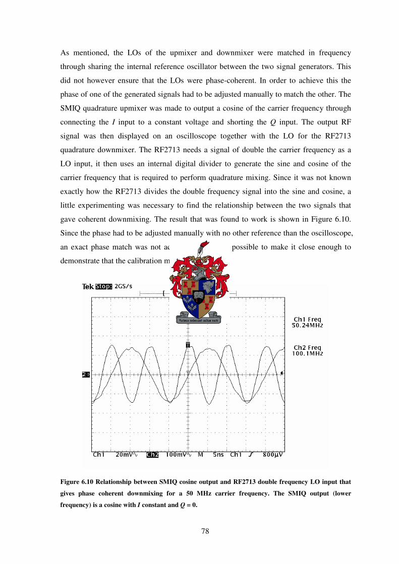
78
As mentioned, the LOs of the upmixer and downmixer were matched in frequency
through sharing the internal reference oscillator between the two signal generators. This
did not however ensure that the LOs were phase-coherent. In order to achieve this the
phase of one of the generated signals had to be adjusted manually to match the other. The
SMIQ quadrature upmixer was made to output a cosine of the carrier frequency through
connecting the I input to a constant voltage and shorting the Q input. The output RF
signal was then displayed on an oscilloscope together with the LO for the RF2713
quadrature downmixer. The RF2713 needs a signal of double the carrier frequency as a
LO input, it then uses an internal digital divider to generate the sine and cosine of the
carrier frequency that is required to perform quadrature mixing. Since it was not known
exactly how the RF2713 divides the double frequency signal into the sine and cosine, a
little experimenting was necessary to find the relationship between the two signals that
gave coherent downmixing. The result that was found to work is shown in Figure 6.10.
Since the phase had to be adjusted manually with no other reference than the oscilloscope,
an exact phase match was not achieved but it was possible to make it close enough to
demonstrate that the calibration method works.
Figure 6.10 Relationship between SMIQ cosine output and RF2713 double frequency LO input that
gives phase coherent downmixing for a 50 MHz carrier frequency. The SMIQ output (lower
frequency) is a cosine with I constant and Q = 0.

79
As described on page 70, a number of samples must be discarded between each
calibration cycle due to the delay in the DAC and ADC. In order not to change the phase
relationship between the transmitter side and the receiver side when doing this, one must
make sure that the samples that are discarded represents a number of full periods of the
signal. Naming the duration of the discarded samples Tdisc, and the calibration signal
period T, this can be expressed as
discTn
T= (6.2)
where n must be an integer. In this case a calibration frequency of 18.3985 kHz was
chosen as for this frequency the 4096 samples that needs to be discarded corresponds to
an even number of samples for the chosen input sample frequency of 120 kS/s:
14096
120 kS/s 6281
18398.5 Hz
⋅= . (6.3)
So for the chosen sample rate and calibration frequency the 4096 samples that are
discarded represents 628 full periods of the signal, which should ensure the phase
relationship between the transmitter side, where the samples are generated and the
compensation takes place, and the receiver side, where the measurements are made, stays
constant.
With the transmitter and receiver LOs perfectly phase-coherent it should have been
possible to fully calibrate the transmitter with only two measurements, one for amplitude
and phase calibration, and one for DC calibration. In this case where such perfect carrier
coherence was not achieved this is not possible. Since the phases measured for the
sideband and DC spurs on the receiver side are not exactly the same as the phases of the
corresponding spurs in the RF spectrum the calculated compensation factors will be
somewhat incorrect. For that reason, multiple iterations of the algorithm are needed, as
that will allow the compensation factors to converge towards the correct values. Figure

80
6.11 show the transmitted RF spectrum after 6 iterations for amplitude/phase and DC
calibration. As can be seen there is a significant improvement for both spurs compared to
the initial spectrum of Figure 6.4. Although both spurs are still clearly visible above the
noise floor, they have been reduced with about 19 dB for the DC spur and 22 dB for the
sideband spur.
Figure 6.11 RF spectrum after transmitter calibration with the direct calculation method. The carrier
spur has been suppressed to −36 dBc, and the sideband spur to −48 dBc.
It has been shown here that all the three methods that were tested were able to calibrate
the transmitter. For both the fast iterative and the gradient search algorithms, the RF
spectrum showed no remnants of the unwanted spurs after calibration. The fast iterative
algorithm was confirmed to converge much faster than the gradient search algorithm. The
direct calculation algorithm did perform relatively poorly, although it demonstrated that it
was able to suppress both the carrier and the sideband spur. The poor performance can be

81
explained by the fact that the LOs of the upmixer and the downmixer were not truly
coherent in this setup. Since there was a constant phase difference between the two LOs,
all the calculations made by the direct calculation algorithm were slightly wrong. Under
these circumstances, the compensation factors converge towards the optimum values,
while under optimal circumstances the compensation factors should have been calculated
correctly on the first iteration. It is believed that the algorithm would have been able to
perform transmitter calibration in 1 iteration (each for amplitude/phase and DC) in a setup
where the same LO could be used for the upmixer and the downmixer.
It has now been showed that both transmitter and receiver can be calibrated according to
the developed principles. Based, on the tests that have been described until now, the
performance of the different algorithms is summarised in Chapter 6.5 on page 85. In the
following section, it will be investigated if the compensation factors, which are found for
one frequency at a specific time, are valid for other nearby frequencies and stays constant
over time.
6.4 Validity and durability of calibration
The concept of calibration as a means of compensating for errors is based on the
assumptions that the errors are constant or changing very slowly. It is therefore very
interesting to investigate if this assumption is true for the system. The tests here were all
done on the receiver, as it was only here that a “real” quadrature mixer was used.
6.4.1 Calibration’s validity over frequency
Much of the literature on compensation of quadrature errors does not take into account
that the quadrature errors may be frequency dependent [4][5][12][22], and the calibration
method developed here is also based on the assumption that the errors are static over the
concerned bandwidth. It is interesting to verify to what degree this assumption holds, and
to do that a few simple tests were performed on the calibrated receiver.
First, a test was done to verify if the compensation factors that are found for one
calibration frequency are valid at other nearby frequencies when downmixing from the
same carrier frequency, i.e. that the quadrature mixing errors have a flat frequency

82
response. The receiver was calibrated at a calibrating frequency of 20 kHz on a carrier
frequency of 100 MHz. The carrier frequency was kept constant while the calibrating
frequency was adjusted up and down and the magnitude of the returning sideband and DC
spurs were measured. The result is shown in Figure 6.12. As can be seen the spurs do
return rather strongly over a bandwidth of just a few kHz, this is particularly true for the
DC spur. This leads to the conclusion that the quadrature mixing errors are indeed largely
frequency dependent.
17 18 19 20 21 22 23
−80
−70
−60
−50
−40
−30
−20
Frequency [kHz]
Mag
nitu
de [d
Bc]
DC spur
Sideband spur
Figure 6.12 The RF2713 quadrature modulator was calibrated at 20 kHz for a carrier frequency of
100 MHz. The plot shows how the DC and sideband spurs return away from the calibration
frequency. The measurements are marked by squares for the sideband spur and diamonds for the
DC spur. The lines are exponential functions that approximate the measured values. Prior to
calibration, the spur magnitudes were −2 dBc for the carrier spur and −32 dBc for the sideband spur.
A second test was done to examine what happens when the calibration frequency stays
the same but the carrier frequency is changed. The results of this test are shown in Figure
6.13. The receiver was again calibrated with a calibrating frequency of 20 kHz at a carrier

83
frequency, fc of 100 MHz. This time the input frequency was kept constant at fc + 20 kHz,
while the carrier frequency, fc was changed. The carrier frequency was changed all the
way down to 50 MHz, and up to 150 MHz. As can be seen from Figure 6.13, the spurs
returned to levels similar to their values before calibration at 50 MHz.
50 60 70 80 90 100 110 120 130 140 150−70
−60
−50
−40
−30
−20
Carrier frequency [MHz]
Mag
nitu
de [d
Bc]
DC spur
Sideband spur
Figure 6.13 The RF2713 was calibrated at 20 kHz for a carrier frequency of 100 MHz. The plot shows
how the carrier and sideband spurs return as the carrier frequency is changed. The measurements
are marked by squares for the sideband spur and diamonds for the DC spur. The lines are
exponential functions that approximate the measured values. Prior to calibration, the spur
magnitudes were −2 dBc for the carrier spur and −32 dBc for the sideband spur.
6.4.2 Calibration’s validity over time
A few simple tests were carried out to verify whether the quadrature errors remain
constant over time when the frequency stays the same. After the initial receiver
calibration described in Figure 6.2 the receiver was tested again at the same frequency
after 2 hours active operation and after 12 hours inactivity. The tests were performed by

84
loading the compensation factors found by the calibration, and measuring the level of the
sideband and DC spurs. The results are shown in Table 6.6. The receiver was operational
in ca 30 minutes prior to the initial calibration, and should thus be warmed up adequately.
The receiver was then operational most of the time until it was tested after ca 2 hours.
Before the last test, it was switched off and left overnight. The test was then performed
immediately after power up the following morning ca 12 hours after the initial calibration.
Spur Before calibration After calibration After 2 h After 12 h
Sideband -32 dBc -85 dBc -55 dBc -51 dBc
DC -2 dBc -72 dBc -47 dBc - 46 dBc
Table 6.6 Sideband and DC spur magnitude relative to signal for the receiver before calibration,
right after, and 2 hours after calibration.
The simple tests performed show that the quadrature mixing errors are indeed varying
with time. It is interesting to see that the largest variation appears within the first 2 hours
of active operation, where the sideband spur grows with 30 dB and the DC spur with 25
dB compared to the right after calibration. The same figures after nearly 10 hours
inactivity and 12 hours after the initial calibration are 34 dB and 26 dB. Still, even after
12 hours the receiver still performs significantly better than before calibration.

85
6.5 Summary of calibration results
Based on the results from the tests, the performance of the different algorithms can be
summarised as in Table 6.7. The performance is expressed as number of samples required
to calibrate all errors. N is the FFT size and B is the size of the buffers in the DAC and
ADCs, i.e. the number of samples that needs to be discarded between each FFT. The
amount of time the calibration takes in seconds can be found by multiplying the figures
from the table with the input sample rate.
Algorithm Receiver calibration
Coherent transmitter calibration
Noncoherent transmitter calibration
Direct calculation N · 2 (N + B) · 2 n / a
Fast iterative N · 3 to 4 (N + B) · 9 to 16 (N + B) · 9 to 16
Gradient search N · 2 (N + B) · 50 to 100 (N + B) · 50 to 100
Table 6.7 Number of samples required to perform calibration with the different calibration methods.
N is the FFT size and B is the ADC and DAC buffer size.
Through practical tests it has been demonstrated that both transmitter and receiver can be
effectively calibrated using the developed method. For receiver calibration and transmitter
calibration with coherent downmixing, the direct calculation algorithm provides the
fastest calibration, and thus it is to be preferred. When the RF spectrum from the
transmitter cannot be coherently downmixed, the fast iterative algorithm is to be preferred
for transmitter calibration.

86
Chapter 7
Conclusion and discussion
This chapter provides an overview of the work presented in the thesis. The developed
calibration method is reviewed, and areas of potential improvement is pointed out.
7.1 Summary of the work that has been done
As was the goal of this work, it has been confirmed that it is possible to compensate for
the three main quadrature errors; amplitude deviation, phase error and DC offset or
oscillator leakthrough via automated calibration. A calibration method has been
developed and implemented, and the method has been tested extensively in simulations
and on a real PC based SDR. The tests have demonstrated that the calibration method can
successfully suppress the unwanted spurious noise, caused by the quadrature errors, to the
level of the quantisation noise floor. This shows that it is indeed possible to overcome the
performance issues of quadrature mixing through digital compensation.
The developed calibration method is based on the property that the different quadrature
errors each produce distinct artefacts in the frequency spectrum. When a single frequency
test tone is input to the system, the quadrature errors can be identified by observing the
frequency spectrum. To perform the task of identifying the quadrature errors and calculate
the corresponding compensation factors, three different algorithms were developed and
tested. The direct calculation method is the most sophisticated of the algorithms and, as
was expected, this algorithm was found to have the best performance. It is to be preferred
when both magnitude and phase of the frequency spectrum can be measured, which is the
case for receiver calibration and for transmitter calibration with coherent downmixing via
an already calibrated receiver. To perform transmitter calibration without coherent
downmixing, the fast iterative method is to be preferred.

87
7.2 Future work
The calibration method that was implemented assumes that the quadrature errors are
frequency independent or static. Although this approach has been shown to increase
performance by reducing the unwanted spurs over a frequency band, it has been found
that full spur suppression, i.e. to the level of the noise floor is only achieved for the
calibration frequency. The tests show that the quadrature errors of the receiver are
frequency dependent, which suggests that a frequency dependent compensation method
would provide further performance enhancements. This is suggested as a topic for further
research. It was also revealed that the quadrature errors are varying somewhat over time,
which suggests that a continuous in-situ compensation scheme would be able to provide
better performance than what can be achieved with calibration.
Furthermore, the scope of this thesis was limited to only investigating errors particular to
quadrature mixing. These errors are however not the only source of unwanted spurious
noise in the frequency spectrum. As was seen in the tests there are also a number of
harmonic spurs present. It would therefore be a natural extension of this work to expand
the calibration method to also cover harmonic compensation.
7.3 Conclusion
The objectives of the thesis was to establish if it is possible to perform fully automated
compensation for quadrature errors, and to implement an automatic calibration system for
a quadrature mixing SDR front end. These goals have been successfully achieved. The
results of this research supports quadrature mixing as a viable RF front end for SDR,
where digital compensation is a possibility and reconfigurability is a requirement.

88
References
[1] ABIDI, A. A., “Direct-Conversion Radio Transceivers for Digital Communications”,
IEEE Journal of Solid-State Circuits, vol. 30, no. 12, December 1995.
[2] ADLINK, “NuDAQ DAQ-2010 4-Ch, Simultaneous, High Performance Multi-
function Data Acquisition Card – User’s Guide”, ADLINK Technology Inc., 2003.
[3] BRIGHAM E. O., “The Fast Fourier Transform and its Applications”, Prentice-
Hall Inc., 1988.
[4] CAVERS, J. K. and LIAO, M. W., “Adaptive Compensation for Imbalance and
Offset Losses in Direct Conversion Transceivers”, IEEE Transactions on Vehicular
Technology, vol. 42, no. 4, November 1993.
[5] CHURCHILL, F. E., OGAR, G. W. and THOMPSON, B. J., “The Correction of I
and Q Errors in a Coherent Processor”, IEEE Transactions on Aerospace and
Electronics Systems, vol. AES-17, no. 1, January 1981.
[6] CRONJÉ, J. J., “Software Architecture Design of a Software Defined Radio System”,
MScEng thesis, University of Stellenbosch, December 2004.
[7] HARRIS, F. J., “On the Use of Windows for Harmonic Analysis with the Discrete
Fourier Transform”, IEEE Proceedings, vol. 66, no. 1, 1978.
[8] KAY, S. M., “Modern Spectral Estimation – Theory and Application”, Prentice-
Hall, 1988.
[9] KINCAID, D. and CHENEY, W., “Numerical Analysis – Mathematics of scientific
computing”, Brooks / Cole, 2002.
[10] LIKHAREV, K.K. and SEMENOV, V.K., “RSFQ Logic / Memory Family: A New
Josephson-Junction Technology for Sub-Terahertz-Clock-Frequency Digital
Systems”, IEEE Transactions on Applied Superconductivity, vol. 1, issue 1, March
1991, pp 3-28.

89
[11] LOURENS, J. G., “Measuring Audio SNR on Digital Broadcast Systems”, IEEE
Transactions on Broadcasting, vol. 40, no. 2, June 1994.
[12] MARCHESANI, R., “Digital Precompensation of Imperfections in Quadrature
Modulators”, IEEE Transactions on Communications, vol. 48, no. 4, April 2000.
[13] MASTA, B., “Gut-Level Fourier Transforms – Part 6: Window shopping”,
http://www.daqarta.com/AUTHOR.HTM, September 1999.
[14] MITOLA, J., “Technical Challenges in the Globalization of Software Radio”, IEEE
Communications Magazine, vol. 37, issue 2, February 1999.
[15] RAZAVI, B., “Design Considerations for Direct-Conversion Receivers”, IEEE
Transactions on Circuits and Systems II, vol. 44, no. 6, June 1997.
[16] RF MICRO DEVICES, “RF 2713 Quadrature Modulator / demodulator”,
http://www.rfmd.com, 2003.
[17] SKLAR, B., “Digital Communications, Fundamentals and Applications”, Prentice
Hall Inc., 1988.
[18] TSURUMI, H. and SUZUKI, Y., “Broadband RF Stage Architechture for Software-
Defined Radio in Handheld Termnial Applications”, IEEE Communications
Magazine, vol. 37, issue 2, February 1999 pp. 90-95.
[19] TUTTLEBEE, W. H. W., Ed., “Software Defined Radio – Baseband Technologies
for 3G Handsets and Basestations”, John Wiley and Sons Ltd., 2004.
[20] TUTTLEBEE, W., “Advances in Software-Defined Radio”, Electronics Systems
and Software, February 2003.
[21] UNIVERSITY OF STELLENBOSCH, “SDR Research Group Home Page”,
http://www.dsp.sun.ac.za/sdr.
[22] VALKAMA, M., RENFORS, M. and KOIVUNEN, V., ”Advanced Methods for I/Q
Imbalance Compensation in Communication Receivers”, IEEE Transactions on
Signal Processing, vol. 49, no. 10, October 2001.
[23] VAN ROOYEN, G.-J., “Quadrature-Baseband Compensation Principles for
Arbitrary-Accuracy Signal Conversion and Processing”, PhD dissertation,
University of Stellenbosch, December 2004.

90
[24] VANCE, I. A. W., “Fully Integrated Radio Paging Receiver”, IEE Proc., vol. 129,
pt. F, no. 1, February 1982.
[25] WEISSTEIN, E. W., "Method of Steepest Descent", MathWorld--A Wolfram Web
Resource, http://mathworld.wolfram.com/MethodofSteepestDescent.html.
[26] WIDROW, B. and STEARNS, S. D., “Adaptive Signal Processing”, Prentice-Hall
Inc, 1985.
[27] YOUNGBLOOD, G., “A Software-Defined Radio for the Masses”, QEX,
Jul/Aug2002.

91
Appendix A
Source code and simulations
Distribution copies of this thesis should come with a CD attached to the back cover. The
CD contains Matlab Simulink simulations as described in the thesis and the source code
that was contributed to the SDR library. If the CD is missing or unreadable, please
contact the author at one of the following email addresses: [email protected] or
The source code and simulations are also available for download from the following
website:
http://www.dsp.sun.ac.za/~christer/Academic/introduction.htm