##asymmetric double quantum wells with smoothed interfaces 2012
TRANSCRIPT

Cent. Eur. J. Phys. • 10(2) • 2012 • 459-469DOI: 10.2478/s11534-011-0108-2
Central European Journal of Physics
Asymmetric double quantum wells with smoothedinterfaces
Research Article
Vladimir Gavryushin1∗
1 Institute of Applied Research and Semiconductor Physics department, Vilnius University,Sauletekio al. 9-III, 10222 Vilnius, Lithuania
Received 26 August 2011; accepted 16 November 2011
Abstract: We have derived and analyzed the wavefunctions and energy states for an asymmetric double quantumwell (ADQW), broadened due to interdiffusion or other static interface disorder effects, within a known dis-creet variable representative approach for solving the one-dimensional Schrodinger equation. The mainadvantage of this approach is that it yields the energy eigenvalues, and the eigenvectors, in semiconductornanostructures of different shapes as well as the strengths of the optical transitions between them. Thebehaviour of ADQW states for the different mutual widths of coupled wells, for the different degree of broad-ening, and under increasing external electric field is investigated. We have found that interface broadeningeffects change and shift energy levels, not monotonously, but the resonant conditions near an energy ofsub-band coupling regions do not strongly distort. Also , it is shown that an external electric field may helpto achieve resonant conditions for inter-sub-band inverse population by intrawell emission of LO-phononsin diffuse ADQW.
PACS (2008): 73.21.Ac, 73.63.Hs
Keywords: multi-barrier quantum well structures • asymmetric double quantum wells • quasi-bound levels • discreetvariable representation • Schrodinger equation© Versita Sp. z o.o.
1. Introduction
When a thin (∼100 A layers of one semiconductor (e.g.GaAs) are sandwiched between layers of another semi-conductor with a larger band gap (e.g. AlGaAs), carri-ers are trapped and confined in two dimensions (2D), dueto the potential barriers. As a result of quantum con-finement, discrete energy states (or ”sub-bands”) occur,which change dramatically electronic and optical proper-
∗E-mail: [email protected]
ties of such structures, known as the quantum wells (QWs).When the quantum wells are coupled there exist probabil-ities for the electron tunnel, which can be in either of thetwo wells. The novel optical properties of the 2D elec-tron gas appear associated with the transitions betweenquantized sub-bands, so called ”inter-sub-band transi-tions”, which correspond to the range from mid-infraredto terahertz (THz) photon energies. They have narrowline-widths and extremely large dipole moments of tran-sitions.
In recent years, there has been considerable interest inasymmetrical multiple-quantum well systems [1], becausemany new optical devices based on inter-sub-band tran-
459
Author copy

Asymmetric double quantum wells with smoothed interfaces
sitions are being developed (”inter-sub-band optoelec-tronics” [2]). This feature could fulfill the need for effi-cient sources of coherent infrared (IR) radiation for sev-eral applications, such as communications, radar, and op-toelectronics. Their most spectacular applications arequantum well IR photodetectors [3] and the quantum cas-cade (QC) lasers [4], that relies on the cascaded inter-sub-band transitions and resonant tunneling between ad-jacent QWs. These devices are made with epitaxiallygrown GaAs/AlGaAs, InGaAs/AlInAs, GaN/AlGaN [1, 5]],and Si/SiGe [6] systems. With the recent developmenton semiconductor device growth technology, multi-barrierquantum well structures are becoming the basic buildingblocks of modern semiconductor devices, such as resonanttunneling diodes (RTD) [7], high-speed light modulators[8, 9], wavelength tunable lasers [10, 11], far-infrared andTHz lasers [12], quantum cascade (QC) lasers [4, 13], etc.In an inter-sub-band quantum cascade laser, the popu-lation inversion must be established by engineering thelifetimes and oscillator strengths, i.e. by a suitable de-sign of the active region. Calculations for quantum wellsare often performed in the approximation where the con-duction and valence band offsets are taken as sharp stepfunctions. In practice, real QW structures tend to deviatefrom the ideal homogeneous heterostructures with perfectabrupt interfaces due to the fluctuations of the band edges(Fig. 1), and inter-diffusion which thus is not very well de-fined. The reasons for this are the stochastic processes ofthe crystal growth leading to local variations of chemi-cal composition, well width, and lattice imperfections toname a few. Since a QW is generally a heterostructureformed by a binary semiconductor (AB) and a ternary dis-ordered alloy (AB1−xCx ), as in GaAs/InGaAs, there aretwo types of disorders responsible for the inhomogeneousbroadening: compositional disorder, caused by concen-tration fluctuations in a ternary component, and randomdiffusion across the interface.Surface segregation during epitaxial growth [14] and ther-mal annealing [15] processes may result in the symmetricinter-diffusion at interfaces [15]. Both processes changethe electronic behaviour of a system by narrowing theQWs and degrading the barriers of QWs. In such inter-diffused or inter-mixed QW structures with smooth inter-face profiles, significant changes in the sub-band spacingand carrier scattering rates in a Si/SiGe QW system [6],were predicted.The inter-diffused QW structures such as GaAs/AlGaAs[16] and InP/InGaAs [17, 18] have been actively investi-gated for improved inter-sub-band electro-absorptive lightmodulation [17, 18], and widely used in several opticaldevices, such as electro-absorptive [19] and lateral con-finement [20] waveguides, light modulators [21, 22], and
wavelength tunable lasers [10, 11]. The improved quan-tum confinement and a higher tunneling rate achieved inthe inter-diffused QW’s cannot be fulfilled by a rectangu-lar QW structure simultaneously. The extensively inter-diffused QW reduces the required bias or increases thetunneling rate for EA modulation. Therefore, the diffusedQW structure is potentially attractive for developing high-speed modulators. The effect of inter-diffusion has beensimulated and investigated below.
The genius of the QW heterostructure concept—and thequantum cascade in particular—lies in its innate engi-neerability. In order to design new devices or optimizethe device performance, and thus properly predict theirbehavior, one needs to know the detailed information ofquasi-bound levels in real disordered multi-barrier quan-tum well structures. Theoretical studies of the influence ofthe compositional and interface disorder on the motion offree carriers in nanostructures have a long history [23–25].There have been calculations for phenomena like excitonlocalization at lateral fluctuations of the well width andband tails [26, 27] as shown in Fig. 1c due to fluctuationsin impurity concentration.
To understand the physical properties of the heterostruc-ture devices, one needs to solve the eigenvalue problemof carriers in QWs. It is well known that exact analyticalsolutions to such problems are only available for simplestructures such as a square or parabolic well [28], and evenin these structures, in general, in the presence of perturba-tions such as external fields, disorder effects [29], etc., theproblem cannot be solved exactly. There have been vari-ous numerical methods used to calculate the band profilesin QWs: the matrix approach (MA) [30, 31], the transfermatrix (TM) method [32, 33], the finite difference method(FDM) [34, 35], the ”shooting method” (SM) [34, 36], the fi-nite element (FE) technique [37, 38], discreet variable rep-resentation (DVR) approach [39], envelope function (EF)method [40], Wentzel–Kramers–Brillouin (WKB) approxi-mation [41], variational method (VM) [42], and Monte Carlo(MC) simulations [43]. Among them, the WKB and EFmethods adopt approximations, thus giving unreliable re-sults; the VM only works well at simple QWs and weakfields; the MC and FE methods are highly computer-orientated approaches; the MA usually require wave func-tion to be well behaved; the SM’s speed comes at thecost of stability. The DVR and TM methods overcome allthe shortcomings listed above and could be easily appliedto any potential profiles of biased/unbiased multi-barrierquantum well structures.In this paper, we describe a numerical technique based onthe DVR approach, as a grid-point representation (griddiscretisation method) of a Hamiltonian matrix element[29, 39, 44] which is capable of solving the eigenvalue and
460
Author copy

Vladimir Gavryushin
Figure 1. a) Characteristic length scales describing the interface roughness of a QW. (b) Spatially locally fluctuating band edges caused by randomdistribution of impurities [46]. (c) Resulting densities of states in the conduction with tail states extending into the forbidden gap. Thedashed lines show the parabolic densities of states in undoped semiconductors.
eigenfunction problems in an arbitrary QW under arbitraryperturbation. Calculation results for energy levels andwave functions of an asymmetric double quantum well withsharp interfaces and inter-diffused interfaces with gradualvariation of the potential, are presented and compared.
2. Calculation details2.1. A model of the interface disorder effectsRandomly distributed charged dopants, or composition xin mixed crystals AxB1−x , lead to unavoidable fluctuationsof the doping impurities concentration on a microscopicscale. Semiconductor heterostructures possess a certaindegree of disorder due to their alloy structure and/or im-perfect interfaces. Two things influence interface disor-der effects: coordinate fluctuations of interface position(Fig 1a), and gap energy Eg(x) fluctuations (Fig. 1b,c)due to the randomly distributed dopants. These fluctua-tions result in potential fluctuations giving rise to bandtails composed from localized states. This situation isschematically shown in Fig. 1. The magnitude of band-edge energy fluctuations (Fig. 1b,c) caused by the randomdistribution of charged donors and acceptors was first cal-culated by Kane [45]. States with energy below the un-perturbed conduction band edge or above the unperturbedvalence band edge are called tail states, which signifi-cantly change the density of states in the vicinity of theband edge.Particularly simple 1D models of an electron moving in arandom or diffused potential are possible. If the fluctu-ations are not too large, good approximation is obtainedby calculating spectra for slightly different configurationsand adding them up using some broadening weight factor.
Inhomogeneous broadening, due to site variation producedby a random distribution of local crystal fields, results ina Gaussian type broadening [45]. Homogeneous broad-ening, from dynamic perturbations on energy levels andequally on all ions, leads to a Lorentzian type broadening.So, a QW’s barrier interface roughness may be approxi-mated [29] by the convolution of Heaviside step functionΦ(x − x0) with an area normalized, a moving Gaussianbroadening envelope function of width σG [45]:
HG(z, z0, σ ) = 1√2πσG
∞∫
0
exp[− (z − x)2
2σ 2G
]Φ(x − z0)dx,
(1)or with the Lorentzian broadening envelope function ofwidth Γ :
HL(z, z0, Γ ) = Γπ
∞∫
0
1(z − x)2 + Γ 2 Φ(x − z0)dx. (2)
A convolution (smoothing) procedure [47] is an integralthat expresses the amount of overlap of envelope function(i.e. Gaussian or Lorentzian) as it is shifted over anotherfunction Φ. Instead of the ∞ limit usually used in inte-gration, we take any value big enough for the resultantconvergence.The barrier steps may also be broadened in an extremelysimple analytical way, - by applying of the phenomeno-logical atan(x) function against the Heaviside step func-tion Φ(x), usual for an ideal heterostructure with perfectinterfaces:
Φ(z − zi)⇒π2 + arctan z − ziΓi
, (3)
461
Author copy

Asymmetric double quantum wells with smoothed interfaces
Figure 2. Comparison of convolution broadenings of the Heavi-side step-function with different broadening functions: 1– Gaussian broadened step; 2 – Gaussian envelope; 3– Lorentzian broadened step; 4 - Lorentzian envelope; 5– Analytical arctan(x) approximation curve (3); Analyticalerror function profile (4) is fully overlapped with curve 1.Broadening parameter Γ = 0.05 nm.
where Γi is the broadening parameter of the interfacesat zi. This function with zero mean zi, characterises thedeviation of the ith interface from its average position. Theinter-diffusion of the QW composition profile is described,usually, by an error function erf(x) [6, 15, 48]:
Φ(z − zi)⇒12
[1 + erf
(z − zi√
2Ld
)]. (4)
The extent of the inter-diffusion process is characterisedby a diffusion length Ld . Examples of calculated functions(1)-(4) are presented in Figure 2. An analytical errorfunction profile (4) is fully overlapped with the Gaussianbroadened step (curve 1). As we see in Figure 2, function(3) (red dots) may be a good approximation for convolutionof Heaviside function by Lorentzian envelope (2) (curve 3).To our knowledge, any attempts to use the Lorentziantype broadening or interdiffusion modeling have been pub-lished, so annealed QW interfaces were simulated belowin such a kind.
2.2. Method of discrete variable representa-tion (DVR)Analytical solutions for asymmetrical double and triplequantum-wells are possible only for unbiased sharp rect-angular QWs [49]. We select discrete variable represen-tation (DVR) as a numerical method [39, 50] for our Math-CAD calculations of a stationary 1D Schrodinger equationfor confined eigenstates. Different types of DVR methodshave found wide applications in different fields of prob-
lems [51, 52]. We also carried out DVR calculations forQWs and unharmonic Morse potential [29, 44].The DVR is a numerical grid-point method in which thematrix elements of the local potential energy operator V(r)is approximated as a diagonal matrix (mnemonic: DVR -diagonal V(r), or Discrete Variable Representation): Vik= 〈φi|V |φk〉 = δikV (xi) [53], and the kinetic energy matrixis full, but it has a simple analytic form, as a sum of 1Dmatrices. DVR method is selected since it avoids havingto evaluate integrals in order to obtain the Hamiltonianmatrix and since an energy truncation procedure allowsthe DVR grid points to be adapted naturally to the shapeof any given potential energy surface. The DVR methodgreatly simplifies the evaluation of Hamiltonian matrix el-ements Hik = 〈φi|H|φk〉 and obtains the eigenstates andeigenvalues by using standard numerical diagonalizationmethods of MathCAD or Mathematica.If we choose an equally spaced grid, xi = iΔx, (i =0, ±1, ±2, ... ±N), then the DVR gives an extremely sim-ple grid-point representation of the kinetic energy matrixTi,k = h2k2
i,k/
2m∗ within the conditional formulation [39]:
�T i,k = g
{π2/
3, i = k2 (−1)i−k
(i−k)2 , i �= k
}. (5)
The only parameter involved being the grid spacing Δxvia an energetically weighted grid parameter g (“energyquantum of the grid”):
g = h2
2m∗
(1
Δx
)2
, (6)
where m∗ is the electron effective mass. So, if the gridpoints are uniformly spaced then numerical solutions of amatrices elements of the full energy Hamiltonian operator
H =�T + V = − h
2
2m∗d2
dx2 + V (x)
is as [39]:
Hi,k =�T i,k + Vi,k = h2
2m(Δx)2 (−1)i−k×
×(π2
3 δi,k + 2(i − k)2 (1− δi,k )
)+ V (xi) δi,k (7)
when the δ-functions are placed on a grid that extendsover the interval x = (-∞,∞). First term in parenthesis isa value of second term in the limit N → ∞ [39].In our calculations the potentials of an ideal and of abroadened biased/unbiased double QW are used as [29]:
V1(xi) = U1 [ 1 + Φ(xi − R1)− Φ(xi)] + Vbias(xi),
462
Author copy
Vladimir Gavryushin
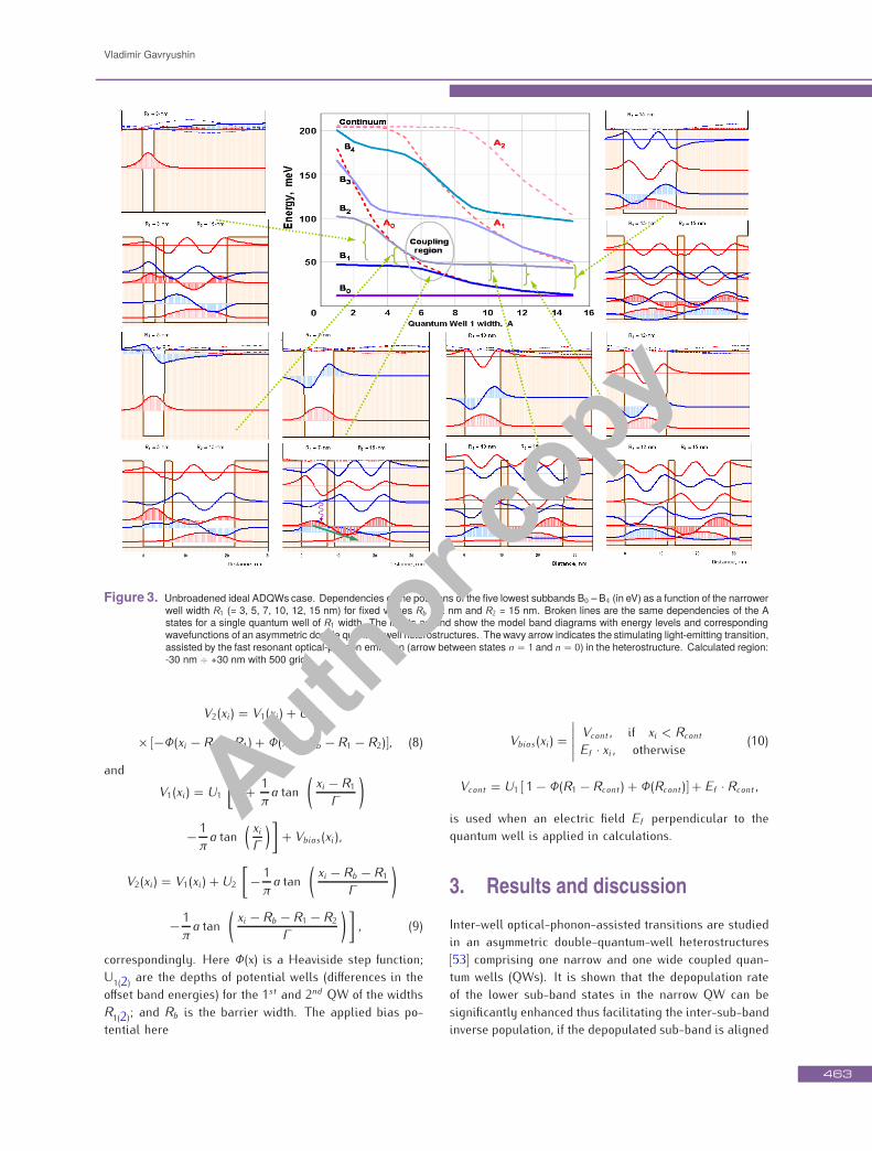
Figure 3. Unbroadened ideal ADQWs case. Dependencies of the positions of the five lowest subbands B0 – B4 (in eV) as a function of the narrowerwell width R1 (= 3, 5, 7, 10, 12, 15 nm) for fixed values Rb = 2 nm and R2 = 15 nm. Broken lines are the same dependencies of the Astates for a single quantum well of R1 width. The insets around show the model band diagrams with energy levels and correspondingwavefunctions of an asymmetric double quantum well heterostructures. The wavy arrow indicates the stimulating light-emitting transition,assisted by the fast resonant optical-phonon emission (arrow between states n = 1 and n = 0) in the heterostructure. Calculated region:-30 nm ÷ +30 nm with 500 grids.
V2(xi) = V1(xi) + U2×
× [−Φ(xi − Rb − R1) + Φ(xi − Rb − R1 − R2)], (8)
andV1(xi) = U1
[1 + 1πa tan
(xi − R1
Γ
)
− 1π a tan
( xiΓ
)]+ Vbias(xi),
V2(xi) = V1(xi) + U2
[− 1π a tan
(xi − Rb − R1
Γ
)
− 1π a tan
(xi − Rb − R1 − R2
Γ
)], (9)
correspondingly. Here Φ(x) is a Heaviside step function;U1(2) are the depths of potential wells (differences in theoffset band energies) for the 1st and 2nd QW of the widthsR1(2); and Rb is the barrier width. The applied bias po-tential here
Vbias(xi) =∣∣∣∣∣Vcont, if xi < RcontEf · xi, otherwise (10)
Vcont = U1 [ 1− Φ(R1 −Rcont ) + Φ(Rcont )] + Ef · Rcont ,
is used when an electric field Ef perpendicular to thequantum well is applied in calculations.
3. Results and discussionInter-well optical-phonon-assisted transitions are studiedin an asymmetric double-quantum-well heterostructures[53] comprising one narrow and one wide coupled quan-tum wells (QWs). It is shown that the depopulation rateof the lower sub-band states in the narrow QW can besignificantly enhanced thus facilitating the inter-sub-bandinverse population, if the depopulated sub-band is aligned
463
Author copy
Asymmetric double quantum wells with smoothed interfaces
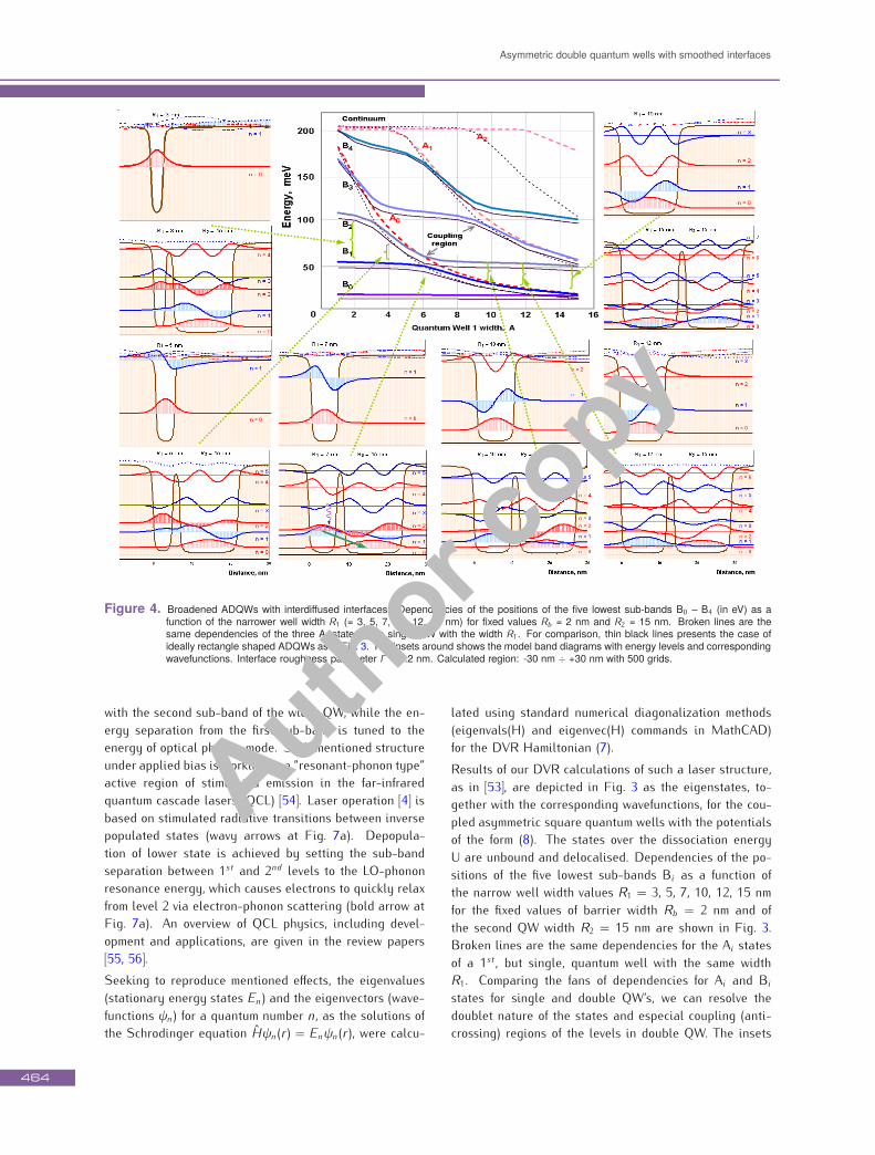
Figure 4. Broadened ADQWs with interdiffused interfaces. Dependencies of the positions of the five lowest sub-bands B0 – B4 (in eV) as afunction of the narrower well width R1 (= 3, 5, 7, 10, 12, 15 nm) for fixed values Rb = 2 nm and R2 = 15 nm. Broken lines are thesame dependencies of the three Ai states for a single QW with the width R1. For comparison, thin black lines presents the case ofideally rectangle shaped ADQWs as in Fig. 3. The insets around shows the model band diagrams with energy levels and correspondingwavefunctions. Interface roughness parameter Γ = 0.2 nm. Calculated region: -30 nm ÷ +30 nm with 500 grids.
with the second sub-band of the wider QW, while the en-ergy separation from the first sub-band is tuned to theenergy of optical phonon mode. Such mentioned structureunder applied bias is working as a ”resonant-phonon type”active region of stimulated emission in the far-infraredquantum cascade lasers (QCL) [54]. Laser operation [4] isbased on stimulated radiative transitions between inversepopulated states (wavy arrows at Fig. 7a). Depopula-tion of lower state is achieved by setting the sub-bandseparation between 1st and 2nd levels to the LO-phononresonance energy, which causes electrons to quickly relaxfrom level 2 via electron-phonon scattering (bold arrow atFig. 7a). An overview of QCL physics, including devel-opment and applications, are given in the review papers[55, 56].Seeking to reproduce mentioned effects, the eigenvalues(stationary energy states En) and the eigenvectors (wave-functions ψn) for a quantum number n, as the solutions ofthe Schrodinger equation Hψn(r) = Enψn(r), were calcu-
lated using standard numerical diagonalization methods(eigenvals(H) and eigenvec(H) commands in MathCAD)for the DVR Hamiltonian (7).Results of our DVR calculations of such a laser structure,as in [53], are depicted in Fig. 3 as the eigenstates, to-gether with the corresponding wavefunctions, for the cou-pled asymmetric square quantum wells with the potentialsof the form (8). The states over the dissociation energyU are unbound and delocalised. Dependencies of the po-sitions of the five lowest sub-bands Bi as a function ofthe narrow well width values R1 = 3, 5, 7, 10, 12, 15 nmfor the fixed values of barrier width Rb = 2 nm and ofthe second QW width R2 = 15 nm are shown in Fig. 3.Broken lines are the same dependencies for the Ai statesof a 1st , but single, quantum well with the same widthR1. Comparing the fans of dependencies for Ai and Bistates for single and double QW’s, we can resolve thedoublet nature of the states and especial coupling (anti-crossing) regions of the levels in double QW. The insets
464
Author copy
Vladimir Gavryushin
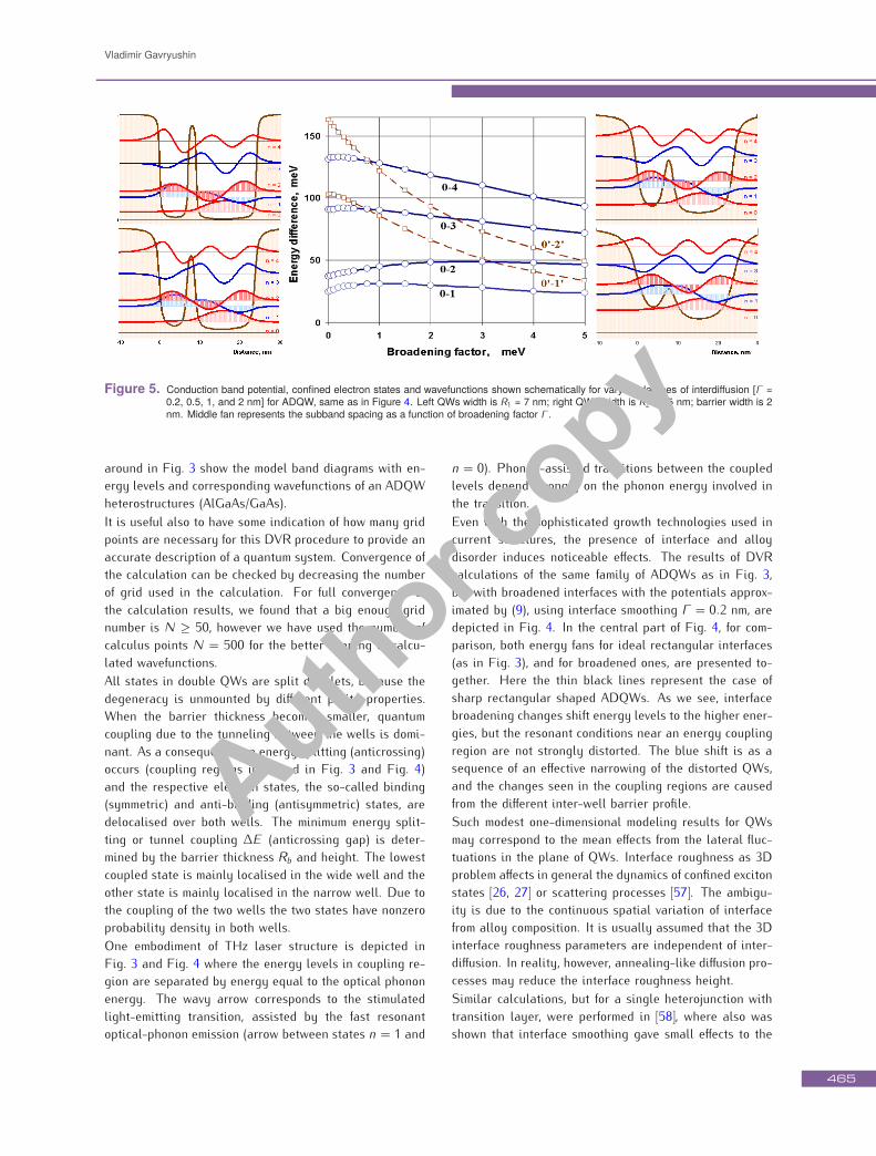
Figure 5. Conduction band potential, confined electron states and wavefunctions shown schematically for varying degrees of interdiffusion [Γ =0.2, 0.5, 1, and 2 nm] for ADQW, same as in Figure 4. Left QWs width is R1 = 7 nm; right QWs width is R2 = 15 nm; barrier width is 2nm. Middle fan represents the subband spacing as a function of broadening factor Γ .
around in Fig. 3 show the model band diagrams with en-ergy levels and corresponding wavefunctions of an ADQWheterostructures (AlGaAs/GaAs).It is useful also to have some indication of how many gridpoints are necessary for this DVR procedure to provide anaccurate description of a quantum system. Convergence ofthe calculation can be checked by decreasing the numberof grid used in the calculation. For full convergence ofthe calculation results, we found that a big enough gridnumber is N ≥ 50, however we have used the number ofcalculus points N = 500 for the better shaping of calcu-lated wavefunctions.All states in double QWs are split doublets, because thedegeneracy is unmounted by different parity properties.When the barrier thickness becomes smaller, quantumcoupling due to the tunneling between the wells is domi-nant. As a consequence, an energy splitting (anticrossing)occurs (coupling regions indicated in Fig. 3 and Fig. 4)and the respective electron states, the so-called binding(symmetric) and anti-binding (antisymmetric) states, aredelocalised over both wells. The minimum energy split-ting or tunnel coupling ΔE (anticrossing gap) is deter-mined by the barrier thickness Rb and height. The lowestcoupled state is mainly localised in the wide well and theother state is mainly localised in the narrow well. Due tothe coupling of the two wells the two states have nonzeroprobability density in both wells.One embodiment of THz laser structure is depicted inFig. 3 and Fig. 4 where the energy levels in coupling re-gion are separated by energy equal to the optical phononenergy. The wavy arrow corresponds to the stimulatedlight-emitting transition, assisted by the fast resonantoptical-phonon emission (arrow between states n = 1 and
n = 0). Phonon-assisted transitions between the coupledlevels depend strongly on the phonon energy involved inthe transition.Even with the sophisticated growth technologies used incurrent structures, the presence of interface and alloydisorder induces noticeable effects. The results of DVRcalculations of the same family of ADQWs as in Fig. 3,but with broadened interfaces with the potentials approx-imated by (9), using interface smoothing Γ = 0.2 nm, aredepicted in Fig. 4. In the central part of Fig. 4, for com-parison, both energy fans for ideal rectangular interfaces(as in Fig. 3), and for broadened ones, are presented to-gether. Here the thin black lines represent the case ofsharp rectangular shaped ADQWs. As we see, interfacebroadening changes shift energy levels to the higher ener-gies, but the resonant conditions near an energy couplingregion are not strongly distorted. The blue shift is as asequence of an effective narrowing of the distorted QWs,and the changes seen in the coupling regions are causedfrom the different inter-well barrier profile.Such modest one-dimensional modeling results for QWsmay correspond to the mean effects from the lateral fluc-tuations in the plane of QWs. Interface roughness as 3Dproblem affects in general the dynamics of confined excitonstates [26, 27] or scattering processes [57]. The ambigu-ity is due to the continuous spatial variation of interfacefrom alloy composition. It is usually assumed that the 3Dinterface roughness parameters are independent of inter-diffusion. In reality, however, annealing-like diffusion pro-cesses may reduce the interface roughness height.Similar calculations, but for a single heterojunction withtransition layer, were performed in [58], where also wasshown that interface smoothing gave small effects to the
465
Author copy

Asymmetric double quantum wells with smoothed interfaces
Figure 6. Confined electron states and wavefunctions dependence on an electric field [E = 0,1.4,2.7,5.4 meV/nm] applied perpendicular to thediffused (Γ = 0.2 nm) ADQW layer plane, same as in Figure 4. Left QW width R1 = 7 nm; right QW width R2 = 15 nm; barrier width is 2nm. Zero external field, or metal contact position Rcont is selected at -7 nm.
energy level differences, - they are relatively insensitiveto the interface profile. Inter-sub-band carrier scatteringin Si/SiGe quantum wells with diffuse interfaces was in-vestigated in [6].
3.1. Effect of the Interdiffusion degree to thestates of ADQW
To estimate the effect of inter-diffusion upon barrier degra-dation [6], same pairs of QWs separated by a thin bar-rier were considered. Figure 5 shows the results for thecoupled diffuse double quantum well, resolving the ef-fect of inter-diffusion degree Γ on the sub-band spacingΔEnn′ . As the broadening factor Γ increases, the bottomof the wells narrow and the top widens. Sub-bands, whichare nominally near the bottom of the well, are thereforepushed up in energy as inter-diffusion increases, whilethose at the top drop relatively in energy. Conversely,the effect is small in sub-bands near the middle of theQW depth.The lower energy electrons are strongly confined in thewider well, and the higher energy electrons in both wells.In the “weak coupling” regime, the sub-band spacing in-creases to a peak shift. At greater inter-diffusion lengths,the sub-band spacing decreases. Inter-diffusion degradesthe barrier between wells. Right-bottom inset of Fig-ure 5 shows the “single well” regime, in which large inter-diffusion merges the wells.Three distinct regimes can be identified, as inter-diffusionincreases. For low inter-diffusion the interfaces are almostabrupt, and the barrier is well defined. This effectively un-couples the wells, resulting in very small overlap between
the lowest pair of sub-bands. As inter-diffusion increases,the barrier degrades and the wells become weakly cou-pled, leading to an increased overlap between sub-bands.The bottoms of the wells narrow, leading to increased sub-band spacing. At very large inter-diffusion lengths, thebarrier potential is substantially reduced, and the systemresembles a single quantum well with the nominal “bar-rier” region acting as a perturbation. The region of over-lap between sub-bands now extends across the entire sys-tem, and the energy spacing between sub-bands is deter-mined approximately by the width of the wide, single welland is hence lower than the nominal value. A blue shiftin the inter-mini-band emission frequency for GaAs/AlAssuperlattices was observed as the inter-diffusion lengthincreased in [59].
3.2. Electric field effect to ADQW states
The resonant situation can be obtained for asymmetriccoupled double quantum wells with applied bias [4, 53, 54].We have performed the same calculations for the diffusedADQW as one of geometry from Figure 4 including theinfluence of an external electric field Ef . Results wereshown at Fig. 6. When an external bias perpendicularto the quantum well is applied, indicated in the Fig. 6by the changed constant slope, electrons are pushed toone side of the well, thus the effective well width is re-duced. At the chosen bias Ef potential tilts downwardsfrom right to left. The middle fan shows how it is possibleto change the resonant conditions of longitudinal optical(LO) phonon emission (breaked arrow) to achieve the in-version population at 3rd state for laser effect with FIR
466
Author copy
Vladimir Gavryushin
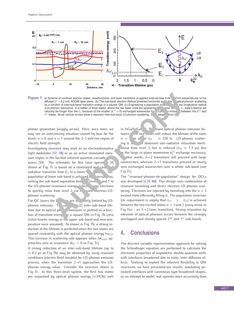
Figure 7. a) Scheme of confined electron states, wavefunctions, and laser transitions at applied external bias 5.44 meV/nm perpendicular to thediffused (Γ = 0.2 nm) ADQW layer plane. (b) The sub-band electron lifetime (inverted horizontal axis) due to optical phonon scatteringas a function of inter-sub-band transition energy in a square QW. (c) Engineering a population inversion using the longitudinal optical(LO) phonon resonance. In a ladder of three states, where the two lower ones are spaced by LO-phonon energy, E3 state’s lifetime willnaturally be longer than the E2 because of the smaller (k12 ≈ 0) exchanged wavevector for LO-phonon emission between the 2nd and1st states. Small vertical arrows show a resonant inter-sub-band LO-phonon scattering. (b,c - adopted from [2])
photon generation (wiggly arrow). Here, once more, wemay see an anticrossing situation caused by bias for thelevels n = 0 and n = 1 around the 2-3 meV/nm region ofelectric field strength.Investigating structure may work as an electroabsorptivelight modulator [17, 18] or as an active stimulated emis-sion region in the far/mid-infrared quantum cascade (QC)lasers [54]. The schematic for this laser operation [4]shown at Fig. 7c is based on a stimulated and cascadedradiative transition from E3 to a lower sub-band E2. De-population of lower sub-band is achieved by external bias,setting the sub-band separation between levels 2 and 1 tothe LO-phonon resonance energy, which causes electronsto quickly relax from level 2 via resonant electron-LO-phonon scattering.For QC lasers the lifetimes are ultimately limited by LO-phonon emission. The computed [2] inter-sub-band life-time due to optical phonon emission, is plotted as a func-tion of transition energy for a square QW in Fig. 7b (zeroinitial kinetic energy in the upper sub-band and zero tem-perature were assumed). As shown in Fig. 7b, a strong re-duction of the lifetime is predicted when the two states arespaced resonantly with the optical phonon energy hωLO .This increase in scattering rate appears when Δkscatt ap-proaches zero at resonance (k21 = 0 in Fig. 7c).A strong reduction of an inter-sub-band lifetime (up to≈ 0.2 ps at Fig 7b) may be obtained by using resonantconditions (electric field tunable) for LO-phonon emissionprocess, when the transition 2→1 approaches the LO-phonon energy value. Consider the structure shown inFig 7c. In this three-level system, the first two statesare separated by optical phonon energy [≈34(36) meV
in InGaAs(GaAs)]. Resonant optical phonon emission be-tween these two states will reduce the lifetime of the staten = 2 to about τ21 ≈ 250 fs. LO-phonon scatter-ing is also the dominant non-radiative relaxation mech-anism from level 3, but is reduced (τ32 ≈ 1.3 ps) dueto the large in-plane momentum k23
|| exchange necessary.In other words, 3→2 transitions will proceed with largewavevectors, whereas 2→1 transitions proceed at nearlyzero exchanged wavevectors over a whole sub-band (seeFig 7c).The ”resonant-phonon-de-population” design for QCLswas developed in [4, 60]. This design uses combination ofresonant tunneling and direct electron-LO-phonon scat-tering. Electrons are injected by tunneling into the n = 3excited state efficiently filling it. The population inversion(its requirement is simply that τ32 > τ21) is achievedbetween the two excited states n = 3 and 2 (wavy arrow inFig 7a,c - as 3→2 laser transition). Strong relaxation byemission of optical phonons occurs between the stronglyoverlapped and closely spaced 2nd and 1st sub-bands.
4. ConclusionsThe discreet variable representation approach for solvingthe Schrodinger equation are performed to calculate theelectronic properties of asymmetric double quantum wellswith interfaces broadened due to static inter-diffusion ef-fects. Seeking to exploit the inherent flexibility in QWstructures, we have presented our results, simulating an-nealed interfaces with Lorentzian type broadened shapes,as an attempt to model real systems more accurately than
467
Author copy
Asymmetric double quantum wells with smoothed interfaces
the abrupt rectangular QW approximation. The wave func-tions and energy states of ADQWs were derived and ana-lyzed in their changes: due to the different mutual widthsof coupled wells, for different degree of the broadening,and under increasing external electric field. Our calcu-lations, however, are simulating the behavior of diffusedelectroabsorptive light modulators [17, 18] and the light-emitter regions of some types of quantum cascade lasers[54].Perhaps the main conclusion of this work is that thekey features for sharp interfaces are preserved, but in-terface broadening effects change and shift energy levels,but not monotonously. The resonant conditions near theenergy of sub-band coupling (anticrossing) regions arenot strongly distorted, but anticrossing energy is slightlygrowing when the interfaces are made smooth. We found,that electric field tunable inter-sub-band energy separa-tions (controlling quantum cascade laser work) were notchanged monotonously on the inter-diffusion level, andtherefore are important for inter-sub-band optoelectron-ics technology predictions [2]. It is shown how externalbias may help to achieve resonant conditions for inversepopulation by intra-well emission of LO-phonons.
AcknowledgmentsThis work was partly supported by the Lithuanian StateScience and Studies Foundation grand.
References
[1] K. Talele, E. P. Samuel, D. S. Patil, Optik 122,626 (2011)
[2] J. Faist, Intersubband optoelectronics (ETH Zurich,Zurich, 2009) www.phys.ethz.ch/∼mesoqc/lectures/QCL-lecture-long.pdf
[3] B. Levine, et al., Appl. Phys. Lett. 50, 1092 (1987)[4] J. Faist et al., Science 264, 553 (1994)[5] J. Faist et al., Appl. Phys. Lett. 67, 3057 (1995)[6] A. Valavanis, Z. Ikonic, R. W. Kelsall, Phys. Rev. B
77, 075312 (2008)[7] T. Sollner, W. Goodhue, P. Tannenwald, C. Parker,
Appl. Phys. Lett. 43, 588 (1983)[8] M. Ghisoni, G. Parry, M. Pate, G. Hill, J. Roberts,
Jpn. J. Appl. Phys. 30, L1018 (1991)[9] W. C. H. Choy, E. H. Li, IEEE J. Quantum Elect. 33,
382 (1997)[10] I. Gontijo, T. Krauss, R. M. De La Rue, J. S. Roberts,
J. H. Marsh, Electron. Lett. 30, 145 (1994)[11] J. J. He, et al., Electron. Lett. 24, 2094 (1995)
[12] R. Kohler, et al., Nature 417, 156 (2002)[13] J. S. Yu, A. Evans, J. David, L. Doris, S. Slivken, M.
Razeghi, IEEE Photonic. Tech. L. 16, 747 (2004)[14] J. Zhang et al., Surf. Sci. 600, 2288 (2006)[15] E. H. Li, B. L. Weiss, K.-S. Chan, IEEE J. Quantum.
Elect. 32, 1399 (1996)[16] W. C. H Choy, E. H. Li, IEEE J. Quantum Elect. 34,
1162 (1998)[17] E. H. Li, IEEE J. Quantum Elect. 34, 982 (1998)[18] E. H. Li, IEEE J. Quantum Elect. 34, 1155 (1998)[19] J. D. Ralston, W. J. Schaff, D. P. Bour, L. F. Eastman,
Appl. Phys. Lett. 54, 534 (1988)[20] J. E. Zucker, et al., Electron. Lett. 28, 853 (1992)[21] M. Ghisoni, G. Parry, M. Pate, G. Hill, J. Roberts,
Jpn. J. Appl. Phys. 30, L1018 (1991)[22] W. C. H. Choy, E. H. Li, IEEE J. Quantum Elect. 33,
382 (1997)[23] A. Efros, M. Raikh, In: R. Elliott, I. Ipatova (Eds.),
Optical properties of mixed crystals (North-Holland,Amsterdam, 1988) 133
[24] M. Herman, D. Bimberg, J. Christen, J. Appl. Phys.70, R1 (1991)
[25] E. Runge, Solid State Phys. 57, 149 (2002)[26] R. Zimmermann, F. Grobe, E. Runge, Pure Appl. Chem.
69, 1179 (1997)[27] E. Runge, Phys. Status Solidi A 201, 389 (2004)[28] H. Wang, H. Xu, Y. Zhang, Phys. Lett. A 340,
347 (2005)[29] V. Gavryushin, SPIE Proc. Ser. 6596, 659619 (2007)[30] A. K. Ghatak, K. Thyagarajan, M. R. Shenoy, Thin
Solid Films 163, 461 (1988)[31] A. K. Ghatak, K. Thyagarajan, M. R. Shenoy, IEEE J.
Quantum Elect. 24, 1524 (1988)[32] E. Anemogiannis, E. N. Glysis, T. F. Gaylord, T.K.
Gaylord, IEEE J. Quantum Elect. 29, 2731 (1993)[33] E. P. Samuel, D. S. Patil, Progress In Electromagnet-
ics Research Letters 1, 119 (2008)[34] P. Harrison, Quantum wells, wires and dots: theoret-
ical and computational physics, 2nd edition (Wiley,Chichester, UK, 2005)
[35] B. M. Stupovski, J. V. Crnjanski, D. M. Gvozdic, Com-put. Phys. Commun. 182, 289 (2011)
[36] S. F.-P. Paul, H. Fouckhardt, Phys. Lett. A 286,199 (2001)
[37] K. Nakamura, A. Shimizu, M. Koshiba, K. Hayata,IEEE J. Quantum Elect. 25, 889 (1989)
[38] K. Q. Le, Microw. Opt. Techn. Let. 51, 1 (2009)[39] D. Colbert, W. Miller, J. Chem. Phys. 96, 1982 (1992)[40] E. J. Austin, M. Jaros, Phys. Rev. B 31, 5569 (1985)[41] J. Heremans, D. L. Partin, P. D. Dresselhaus, Appl.
Phys. Lett. 48, 644 (1986)[42] D. Ahn, S. L. Chuang, Appl. Phys. Lett. 49,
468
Author copy

Vladimir Gavryushin
1450 (1986)[43] J. Singh, Appl. Phys. Lett. 48, 434 (1986)[44] V. Gavryushin, arXiv:q-bio/0510041v1 [q-bio.BM][45] E. O. Kane, Phys. Rev. 131, 79 (1963)[46] J. I. Pankove, Optical processes in semiconductors
(Dover Publications Inc., New York, 1975)[47] E. W. Weisstein, Convolution. Wolfram Web Resource:
http://mathworld.wolfram.com/Convolution.html[48] T. E. Scholesinger, T. Kuech, Appl. Phys. Lett. 49,
519 (1986)[49] R. Betancourt-Riera, R. Rosas, I. Marin-Enriquez, R.
Riera, J. L. Marin, J. Phys. C 17, 4451 (2005)[50] G. W. Wei, J. Phys. B 33, 343 (2000)[51] H.S. Lee, J. Light, J. Chem. Phys. 120, 4626 (2004)[52] J. Tennyson, et al., Comput. Phys. Commun. 163,
85 (2004)
[53] M. A. Stroscio, M. Kisin, G. Belenky, S. Luryi, Appl.Phys. Lett. 75, 3258 (1999)
[54] J. Faist, F. Capasso, C. Sirtori, D. L. Sivco, A. Y. Cho,In: H. C. Liu, F. Capasso (Eds.), Intersubband tran-sitions in quantum wells: physics and device appli-cations, nr. 2, ch. VIII. (Academic Press, New York,2000)
[55] F. Capasso, et al., J. Quantum Elect. 38, 511 (2002)[56] J. Faist et al., J. Quantum Elect. 38, 533 (2002)[57] A. Leuliet et al., Phys. Rev. B 73, 085311 (2006)[58] F. Stern, S. Das Sarma, Phys. Rev. B 30, 840 (1984)[59] T. Roch, C. Pugl, A. M. Andrews, W. Schrenk, G.
Strasser, J. Phys. D 38, A132 (2005)[60] B. S. Williams, H. Callebaut, S. Kumar, Q. Hu, J. L.
Reno, Appl. Phys. Lett. 82, 1015 (2003)
469
Author copy