area complexity estimation for combinational logic …jayantt/masters_thesis.pdf · ·...
TRANSCRIPT

Area Complexity Estimation for Combinational Logic
using Fourier Transform on Boolean Cube
A THESIS
submitted by
JAYANT THATTE
in partial fulfilment of the requirements
for the award of the degree of
MASTER OF TECHNOLOGY
DEPARTMENT OF ELECTRICAL ENGINEERINGINDIAN INSTITUTE OF TECHNOLOGY MADRAS.
APRIL 2014

THESIS CERTIFICATE
This is to certify that the thesis titled Area Complexity Estimation for
Combinational Logic using Fourier Transform on Boolean Cube, submitted by
Jayant Thatte, to the Indian Institute of Technology, Madras, for the award of the
degree of Master of Technology, is a bona fide record of the research work done by
him under our supervision. The contents of this thesis, in full or in parts, have not been
submitted to any other Institute or University for the award of any degree or diploma.
Dr. Shankar BalachandranResearch GuideAssistant ProfessorDept. of Computer ScienceIIT-Madras, 600 036
Place: Chennai
Date:
ACKNOWLEDGEMENTS
Any research is not possible without the combined efforts of many people, and this
work is no different. I thank my thesis advisor, Dr. Shankar Balachandran, who has
been a constant guiding support for my research throughout the duration of this project.
I also thank Dr. Nitin Chandrachoodan for agreeing to be co-guide for my project. I
am indebted to Ankit Kagliwal whose Master’s project served as a motivation for this
research problem. I would like to thank Prof. Anand Raghunathan, Purdue University
and Swagath Venkataramani, Purdue University for their inputs and help. It was a great
experience to collaborate with Chaitra Yarlagadda on certain parts of this project.
I am truly grateful to a number of professors who have played a key role in building
the foundation for this project and for my future endeavours. I am thankful of all my
colleagues in RISE Lab. I am also grateful to Department of Computer Science and
Engineering, IIT Madras and Department of Electrical Engineering, IIT Madras for
academic and administrative support. I thank the staff in coffee shop, which has been the
hub for stimulating and lively discussions for most students in the department, including
myself.
I thank Seshan and Siddartha, for all the informative discussions I had with them. I
would like to thank Abraham for helping me out with Linux and LATEX glitches, time
and again, and Nitish, for helping me set-up some of the software platforms that were
used for this project. I thank Prakruthi, Meghana, Chitra, Anuja, Ankit, Soorya, Sohini,
Jobin, Girish, Anand and Akshay for making my stay at IIT Madras pleasant, wonderful
and memorable. I also thank my batch-mates for letting me experience a productive
and fun-filled undergraduate life at IIT Madras. Finally, I would like to pay my highest
regards to my parents for their motivation and support without which my academic
journey would not have been possible.
i
ABSTRACT
KEYWORDS: Fourier Theory; Area Complexity; Logic synthesis; Boolean Cube.
Logic synthesis deals with obtaining the minimized equivalent representation of a
Boolean function and mapping it to minimum number of logic gates available. A
complex logic function requires more physical space on a chip, and incurs higher
manufacturing cost in terms of time and money. This motivates the study of area
complexity of circuits. This problem relates with obtaining a measure of the area
requirement of the circuit without actually mapping it to a gate-library. Mapping
circuits to a gate library is computationally taxing and time-consuming, especially as
the number of inputs increases. Getting an estimate of area requirement of circuits
without going through the logic design flow is therefore very useful.
Moreover, the results obtained using synthesis and mapping are heavily dependent
on the synthesis tool and the mapping library used. In this thesis, an effort has been
made to capture the inherent hardness of a Boolean function that is a fundamental
outcome of its truth table and is independent of Boolean optimisation techniques and
technology. The idea is to get an estimate of this inherent hardness of the function,
treating it solely as a mathematical entity, without bringing into the picture the
variations and bias introduced my electronic design flow tools.
For a combinational circuit, area-complexity is a measure that estimates the logic
area of the circuit without mapping to logic gates. Several measures like literal count,
number of primary input/outputs, etc. have been used in the past to measure area-
complexity. More recently, there have been efforts to measure area-complexity using
the theory of Boolean Difference and Taylor Expansion for Boolean function.
In this thesis, Fourier Theory for Boolean Cube is studied and an effort has been
made to interpret the Fourier coefficients to get a better understanding of
combinational circuits. A novel area-complexity measure using Fourier Theory
applied on Boolean functions is proposed in this work. How the area-complexity of
ii

circuits can be captured using the energy distribution in the Fourier spectrum of these
Boolean functions has been demonstrated. The proposed area complexity metric was
evaluated on a sizeable collection of randomly generated circuits and area and gate
count estimates were computed. The results were then compared against area, gate
count and run time corresponding to traditional logic synthesis using Berkeley SIS
package with MCNC library. The proposed area complexity metric is accurate within
10% (within 5% for 95% of the predictions). Also, estimating area using Fourier
Transform approach poses significantly smaller computational effort as compared to
traditional logic synthesis and the computing effort versus number of inputs, outputs
rises as a much slower exponential when measured against the traditional approach.
The proposed method achieves a speed up of more than 15 times over logic synthesis
for circuits with 10 inputs of more and 5 outputs of more. Finally, the results obtained
using the area-complexity metric are compared with those given by Synopsys Design
Compiler using NanGate 45nm Library to ensure robustness of the proposed metric
with respect to logic synthesis platforms and technologies.
iii

TABLE OF CONTENTS
ACKNOWLEDGEMENTS i
ABSTRACT ii
LIST OF TABLES vi
LIST OF FIGURES viii
ABBREVIATIONS viii
NOTATION ix
1 INTRODUCTION 1
1.1 Motivation . . . . . . . . . . . . . . . . . . . . . . . . . . . . . . . 2
1.2 Related Work . . . . . . . . . . . . . . . . . . . . . . . . . . . . . 4
1.3 Application . . . . . . . . . . . . . . . . . . . . . . . . . . . . . . 7
1.4 Contribution of the Thesis . . . . . . . . . . . . . . . . . . . . . . 8
1.5 Organisation of the Thesis . . . . . . . . . . . . . . . . . . . . . . 8
2 BACKGROUND 10
2.1 Terms and Definitions Pertaining to Boolean Logic . . . . . . . . . 10
2.2 Mathematical Background . . . . . . . . . . . . . . . . . . . . . . 11
2.2.1 The Concept of a Field . . . . . . . . . . . . . . . . . . . . 12
2.2.2 Galois Field and Digital Logic . . . . . . . . . . . . . . . . 14
2.2.3 Shannon’s Expansion . . . . . . . . . . . . . . . . . . . . . 15
2.2.4 Boolean Difference . . . . . . . . . . . . . . . . . . . . . . 15
2.2.5 Taylor Series Expansion . . . . . . . . . . . . . . . . . . . 16
2.2.6 Fourier Transform . . . . . . . . . . . . . . . . . . . . . . 17
2.2.7 XOR Property of Fourier Transform . . . . . . . . . . . . . 18
2.3 Logic Synthesis Packages and Libraries . . . . . . . . . . . . . . . 23
2.3.1 SIS . . . . . . . . . . . . . . . . . . . . . . . . . . . . . . 24
iv

2.3.2 Synopsys Design Compiler . . . . . . . . . . . . . . . . . . 24
2.3.3 MCNC Genlib . . . . . . . . . . . . . . . . . . . . . . . . 24
2.3.4 NanGate 45nm Library . . . . . . . . . . . . . . . . . . . . 25
2.3.5 BLIF Circuit Specification Format . . . . . . . . . . . . . . 25
3 AREA COMPLEXITY USING FOURIER TRANSFORM 26
3.1 Basic Idea . . . . . . . . . . . . . . . . . . . . . . . . . . . . . . . 26
3.1.1 Frequency Levels . . . . . . . . . . . . . . . . . . . . . . . 27
3.2 Problem Type 1: Identifying Optimum Circuit . . . . . . . . . . . . 29
3.3 Problem Type 2: Estimating the Area and Gate Count . . . . . . . . 32
3.4 Multi-Output Circuits . . . . . . . . . . . . . . . . . . . . . . . . . 33
4 RESULTS: METRIC ACCURACY AND TIMING PERFORMANCE 35
4.1 Methodology . . . . . . . . . . . . . . . . . . . . . . . . . . . . . 35
4.2 Accuracy of Predicted Area . . . . . . . . . . . . . . . . . . . . . . 35
4.3 Timing Performance of the Proposed Metric . . . . . . . . . . . . . 39
5 CONCLUSION AND FUTURE WORK 42
5.1 Summary of Results . . . . . . . . . . . . . . . . . . . . . . . . . . 42
5.2 Future Work . . . . . . . . . . . . . . . . . . . . . . . . . . . . . . 44
LIST OF TABLES
2.1 Definition of order 2 Galois Field . . . . . . . . . . . . . . . . . . . 14
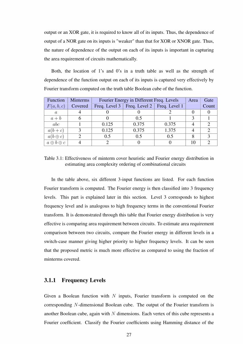
3.1 Effectiveness of minterm cover heuristic and Fourier energy distributionin estimating area complexity ordering of combinational circuits . . 27
vi

LIST OF FIGURES
1.1 Electronic Design Automation Flow . . . . . . . . . . . . . . . . . 2
2.1 ON, OFF and DC sets for a 3-input Boolean function . . . . . . . . 11
3.1 Frequency Levels for a 3-dimensional Boolean Cube . . . . . . . . 28
3.2 Flow chart depicting the algorithm to design approximate circuits . . 31
4.1 Ordering of 128 3-input circuits based on predicted hardness using allFourier coefficients (left) and using only highest two frequency levels(right). X-axis represents an abstract complexity measure computedfrom Fourier coefficients without using regression and Y-axis containsthe actual area post synthesis and mapping. . . . . . . . . . . . . . 36
4.2 Classification of 128 3-input circuits, based only on the highestfrequency coefficient of Fourier transform. X-axis represents abstractarea-complexity metric computed using all Fourier coefficients andY-axis gives the actual area post synthesis. The clusters marked on thegraph are obtained using only the highest frequency coefficient. Noticethat using only this one coefficient, it is possible to classify circuitsinto rough groups based on their hardness and area-requirement. . . 37
4.3 Predicted versus actual area (left) and gate-count (right) for 1000randomly generated 10 input, 1 output circuits. Blue points representdata and the green line represents is “X=Y”. . . . . . . . . . . . . . 37
4.4 Predicted versus actual area (left) and gate-count (right) for 400randomly generated 10 input, 4 output circuits. Blue points representdata and the green line represents “X=Y”. . . . . . . . . . . . . . . 38
4.5 Standard deviation of relative error for varying number of inputs (left)and outputs (right). The blue line displays relative error for gate-countand the green line gives that for predicted area. . . . . . . . . . . . 38
4.6 The graph shows the computational time required for processing 1500randomly generated circuits for varying number of outputs (left). Thegraph (right) shows the average computation time required forprocessing 1 circuit, averaged over 2000 randomly generated circuits.The green line represents the time taken by the traditional method andthe blue line represents the time taken by the proposed approach. . . 39
4.7 The graph shows the average computation time required per circuit peroutput, averaged over 2000 randomly generated circuits. The green linerepresents the time taken by the traditional method and the blue linerepresents the time taken by the proposed approach. . . . . . . . . . 40
vii
ABBREVIATIONS
BDD Binary Decision Diagram
CAD Computer-Aided Designing
EDA Electronic Design Automation
MCNC Microelectronics Center of North Carolina (circuit library for logic synthesis)
SIS Sequential Interactive System (logic synthesis package developed at Berkeley)
SoP Sum-of-Products
VLSI Very Large Scale Integration
DTFS Discrete Time Fourier Series
viii
NOTATION
B Binary set 0, 1Bn Boolean Cube of n dimensions, same as 0, 1nBx The set containing logic ‘True’, ‘False’ and ‘Don’t Care’,
denoted by 0, 1,− or 0, 1,×x Logical complement of Boolean variable x− Logical don’t careφ Empty setΩ Universal Set3 Such thatS1 × S2 Cartesian product of sets S1 and S2
(S, •) Binary structure of set S and binary operation •GF (2) Galois Field of order 2Fx Cofactor of Boolean function F with respect to a Boolean variable x⊕b Bitwise XOR∧b Bitwise ANDj Square root of -1a · b Dot product of vectors a and b
ix
CHAPTER 1
INTRODUCTION
Very Large Scale Integration (VLSI) refers to the process of creating integrated chips
containing millions of transistors packed together in a chip. Over the years, the circuits
implemented inside these chips have become huge and complicated making manual
optimization of the circuit impossible. Today more and more complex logic is being
transferred on smaller and smaller chips. This is possible only with the intervention
of computer aided tools which can automate the process of chip manufacturing. As a
result, many computer-aided designing (CAD) tools have been developed which can
automate chip manufacturing process.
Electronic Design Automation (EDA) refers to a fixed set of steps followed by
many VLSI-CAD tools for circuit design and chip manufacturing. Fig. 1.1 shows the
different steps in the EDA flow. The process starts with a circuit specification which is
abstracted by the tool into computer understandable representation. The circuit is then
“synthesized” which transforms the circuit specification in terms of basic logic gates.
A blueprint of this network of gates needs to be prepared which is done by the physical
design optimization phase. Once the blueprint is ready, actual manufacturing of chips
take place. Each step in the CAD flow in-turn has a series of algorithms which
optimize one or the other parameters of the circuit. e.g. Physical design aims at
optimizing the layout area, the routing space, etc. Wang et al. (2009) provides a
detailed explanation for each step in the EDA flow.
Logic synthesis is a process which transforms the desired circuit functionality into
a network of logic gates. The different steps in logic synthesis are: (a) abstraction of
the circuit specification into a Boolean network, (b) minimization of the network and
(c) mapping it in terms of given gate-library. Logic synthesis is broadly classified as
technology independent synthesis and technology dependent synthesis. In technology
independent synthesis, initial circuit representation is in terms of basic logic gates
(such as AND, OR and NOT). At this point, the smallest representation of the circuit is
obtained using various optimization algorithms. This phase is also called as logic

Figure 1.1: Electronic Design Automation Flow
minimization or logic optimization. The next step is the technology mapping phase
where the circuit is implemented in terms of specific libraries of cells. Once
technology mapping is done, timing and power optimizations are performed. Finally
the circuit is ready for the layout and manufacturing processes. Of the vast field of
logic synthesis, we study logic minimization in detail.
Logic minimization deals with obtaining the smallest equivalent representation of
a given Boolean function. This research explores the concept of area complexity of
circuits. This problem relates with obtaining a measure of the area requirement of the
circuit without actually mapping it to a gate-library.
1.1 Motivation
A complex circuit requires more physical space on a chip, and incurs higher
manufacturing cost in terms of time and money. This motivates the study of logic
minimization. This motivates the study of logic minimization. Studying
area-complexity of a function is useful as it gives a hint of how “complex” the function
2

is. Using the concept of area-complexity, more resources can be spent to optimize a
logically “complex” function than a simple one.
Area-complexity of a logic circuit refers to estimation of the logic area required by
the circuit without actually mapping it to logic gates. The area complexity of a circuit
can be measured in terms of the number of inputs, literals, logic gates, etc. With the
advancement of technology, the logic circuits are increasing in size and becoming more
complicated. To aid the CAD tools in optimizing such large circuits, it is necessary to
associate some parameter with the circuits at the logic optimization level itself. The
only available description of the circuit at this level is the functional description of the
circuit. Area-complexity of a circuit is one such measure which utilizes the functional
description and gives a qualitative comparison between different circuits. Designing
an area-complexity measure which is quick and effective in analysing the functions
at the logic optimization phase forms the motivation behind studying area-complexity
problem.
Moreover, the results obtained using synthesis and mapping are heavily dependent
on the synthesis tool and the mapping library used. The idea is to get an estimate of this
inherent hardness of the function, treating it solely as a mathematical entity, without
bringing into the picture the variations and bias introduced my electronic design flow
tools. With this motivation, an effort has been made to capture the inherent hardness of
a Boolean function that is a fundamental outcome of its truth table and is independent
of Boolean optimisation techniques and technology.
Over the past few decades, there has been a rapidly increasing effort to shrink all
electronic systems and to pack larger functionality on the same area of silicon. The area
footprint of functions on silicon after logic synthesis has therefore become of utmost
importance. The layout area occupied by Boolean circuits is considered as a complexity
measure of Boolean functions. Traditionally, it is known that functions with roughly
equal number of 1s and 0s in their truth table are more complex than those whose truth
tables are dominated by 1s or 0s. For example, n-input AND, n-input OR are much
simpler than n-input parity function. However, this conventional approach fails in many
cases. For example, n-input XOR is much more complex than the function where output
is equal to one of the inputs (the rest being don’t cares) even though both have exactly
equal number of 1s and 0s. Clearly, not only the number, but also the placement of 1s
3
and 0s in the truth table is what decides the complexity of Boolean functions. Another
technique which is used is called Literal Count which is the sum of the number of times
each literal appears in an expression. This metric works for small number of inputs,
but as the number of inputs increases, the predicted complexity is much higher than the
actual.
From information theory point of view, a Boolean function is more complex if more
inputs need to be fixed to fix the output. For example, an n-input XOR function needs
all n of its inputs to be fixed to fix the output as opposed to AND or OR gates where
a single input may be sufficient to determine the output. The output of an AND gate
is said to depend weakly on each of its inputs, that is knowledge of state of each input
is not necessarily essential in determining the state of the output. As against this, each
input of an XOR gate necessarily needs to be known to determine its output. The output
of XOR gate is therefore said to depend strongly on each of its inputs. Thus, a function
which depends on all of its inputs is more complex than one which depends only on few
of them. Moreover, stronger the dependence, more complex the circuit. Dependence
of output on each of the inputs comes out naturally using the technique of Fourier
Transform with each input being an independent dimension. Studying Fourier Theory
for Boolean Cube in the context of circuit complexity is, therefore, of great interest.
Studying Fourier spectrum of circuits reveals several interesting properties. We show
that studying the Fourier spectrum of circuits is an effective way of getting an estimate
on the area requirement of circuits without going through the complete electronic design
flow.
Note: An n-dimensional Boolean cube represents the set of all possible binary
strings of length n. 1-D and 2-D Boolean cubes should be called Boolean line and
Boolean square respectively. Similarly a Boolean cube in more than 3 dimensions
should be called a Boolean hypercube. However, throughout this dissertation, we will
use the term Boolean cube even when the number of dimensions is other than 3.
1.2 Related Work
This section presents the related work for the problems considered in this thesis. A brief
description of the different area-complexity metrics designed till date has been provided
4
in this section.
The area-complexity of a circuit can be measured in terms of the number of inputs or
literals or gates, etc. Characterizing logic functions and estimation of area-complexity
dates back to 1949 when Shannon (1949) measured the area-complexity as the amount
of switching activity in the circuit. The switching activity was captured by the number
of relay elements in the circuit. In that paper, Shannon proved that the asymptotic
complexity of a Boolean function is exponential in terms of number of primary inputs.
He also showed that for large number of primary inputs, almost every Boolean function
is exponentially complex.
Muller (1956) established that the number of logic gates (gate-count) can be used
to estimate the area of a circuit. An important result of Muller’s work is that the area-
complexity measure based on the gate-count is independent of the underlying gate-
library. Cook (1973) used the concept of entropy of a truth table (the probability of
finding a “1” in the truth table) to get an estimate of area complexity of the Boolean
function. In Pippenger (1976), the author presents an extensive study of relationship
between circuit complexity and information theory, from a theoretical stand-point.
Cheng and Agarwal (1990) used the number of literals in the Boolean equation
(literal-count) to measure area-complexity. They also established the relation between
area-complexity and entropy of the circuit. Entropy of a circuit is defined as the amount
of information stored in the circuit. Only small circuits (inputs less than ten) were used
to demonstrate the relation. For larger circuits, the area predicted was exponentially
high while the circuit required much less gates. e.g., as Nemani and Najm (1996)
points out, for a 32-input Boolean function, the area predicted by this model is around
400 million gates, whereas the circuit can actually be implemented using 84 gates.
The methods proposed by Wu et al. (1991) and Kurdahi (1993) use sum-of-products
(SoP) representation to estimate the area-complexity. They measure area-complexity in
terms of total number of AND and OR gates. This can lead to over-prediction of the
number of gates as frequent application of logic synthesis algorithms often reduces the
gate-count.
In Nemani et al. (1999), the authors proposed an area and power estimation metric
based on the functional description (Boolean equation) of the circuit. The metric uses
5
the size of prime implicants in the ON-set and the OFF-set of the circuit to estimate
the gate-count. The drawback of this approach is that the presence of simple implicants
(containing single literals) in the circuit affects the accuracy of the metric.
With rising popularity of BDDs (binary decision diagrams) in the 1990’s, many
area-complexity metrics based on the structural parameters of the BDDs have been
proposed. Drechsler and Sieling (2001); Raseen et al. (2006); Beg and C. (2010) used
the number of nodes in the BDD representation of a function as an area complexity
measure.
More recently, in Kagliwal and Balachandran (2013) area-complexity measure
using the theory of Boolean difference and Taylor expansion for Boolean functions
was proposed. This concept of using order 2 Galois Field (denoted as, GF (2)) algebra
to mathematically estimate area and gate-count has been taken further in this thesis
using the more natural approach of Fourier Transforms to capture the dependence of
the function output on its inputs.
There have been research papers which study Fourier Theory over GF (2), from
mathematics theory point of view. In de Wolf (2008), the author has presented an
extensive study of Fourier Transform on Boolean Cube and its properties and
implication from a theoretical perspective. However, so far, there has been no effort in
combining this theoretical field of Fourier Theory on Boolean Cube with digital circuit
design and logic optimisation. In this thesis, an effort has been made to combine these
two areas of knowledge to arrive at a practically useful algorithm to estimate area
complexity of circuits without going through the traditional circuit design flow.
Final chapter of this thesis talks about the concept of approximate computing or
best-effort computing and the potential that the proposed area estimation approach has
for its use in systematically designing approximate circuits while maintaining a low
run time. Approximate computing refers to circuits which approximate the
functionality of a target circuit within a specified tolerance limit, thus achieving a
significant reduction in area and power consumption. With space on Silicon becoming
increasingly important, there has been a lot of effort in the recent years to study the
concept of approximate computing and to design approximate circuits in an automated
manner. In Kravets and Kudva (2003), the authors have examined a logic restructuring
approach to achieve improved routing.
6

In Venkataramani et al. (2012), a systematic method to design approximate circuits
has been presented. The authors make use of traditional don’t care based optimisation
in logic synthesis tools to design circuits with reduced area and power consumption
while still ensuring that the circuit meets the quality constraints at all stages of
approximation. Combining the methodology presented in this paper with the idea
presented in this thesis is an interesting research problem for future work. If
successful, it would give a very useful algorithm for systematically designing
approximate circuits with a significantly smaller computing effort.
1.3 Application
Area-complexity refers to predicting the logic area requirement of a circuit without
performing technology mapping. Estimation of area-complexity has wide applications
in logic synthesis framework. Many CAD tools implement different area-complexity
metrics to distinguish between simple and complicated circuit. If a function can be
categorized according to its level of complication early in the logic synthesis flow, the
CAD tools can configure themselves effectively to optimize the circuit. The primary
aim of area-complexity is to measure area requirement of the circuit. However, many
researchers have proposed to use area-complexity of a circuit to design power
estimation models for the circuit Nemani et al. (1999).
The idea of estimating area complexity using Fourier coefficients can be combined
with the developing area of approximate computing to systematically design
approximate circuits that have significantly smaller area and power consumption while
simultaneously meeting the quality constraints imposed by the user. Designing of
approximate circuits involves systematic, step-by-step approximation of the original
circuit to achieve area reduction at each stage of approximation. To do this, the area
occupied by the circuit should be known or estimated at each stage of approximation.
Using the proposed approach of estimating the area requirement of circuits in this
context will help in systematically designing approximate circuits with a substantially
smaller computing effort.
7
1.4 Contribution of the Thesis
The contributions of the thesis are:
1. A novel area complexity metric based on Fourier coefficients of Boolean Cube isproposed. Using statistical analysis on a sizeable collection of randomlygenerated circuits, it is demonstrated that the proposed metric is effective inestimating the area-complexity of Boolean circuits.
2. The new area-complexity metric is accurate within 10% (within 5% for 95% ofthe data points) of the actual area and number of gates obtained using BerkeleySIS package with MCNC library as opposed to at least 100%, 15% and 10%respectively for the metrics based on literal-count, BDD properties and thecomplexity metric based on Boolean difference and Taylor series proposed inKagliwal and Balachandran (2013). Finally, the results obtained using the metricare also compared with those obtained using Synopsys Design Compiler withNanGate 45nm Library.
3. The proposed approach poses a much smaller computational complexity ascompared to traditional logic synthesis approach. The dependence of run timeon number of inputs and outputs is a much slower rising exponential than thatfor actual logic synthesis. The new approach achieves a speed up of more than15 times over logic synthesis for circuits with 10 inputs of more and 5 outputs ofmore.
1.5 Organisation of the Thesis
This dissertation is organised into six chapters. The first chapter provides an
introduction to the process of logic synthesis and explains the motivation behind
exploring the proposed area-complexity metric. A later section in this chapter
discusses related work for the problem presented in this thesis. Chapter 2 gives a
background on the mathematical theory required for understanding the proposed
area-complexity metric and also gives information necessary to understand various
terms and definitions in logic synthesis. It also gives an insight into the logic synthesis
tools and libraries used for this project. In Chapter 3, the proposed area-complexity
metric using Fourier coefficients of Boolean Cube is presented. The metric is
evaluated using a statistically significant collection of randomly generated circuits and
the results in terms of area, gate-count and run time are compared with the outputs
obtained from logic synthesis using Berkeley SIS package using MCNC Library. The
metric results are then also compared with those obtained from Synopsys Design
8
Compiler using standard NanGate 45nm Library to ensure robustness of the proposed
metric. All of the results are detailed out in Chapter 4. Chapter 5 touches upon the area
of approximate computing and outlines the possibility of using the proposed metric to
systematically design approximate circuits. This chapter also states the specific
problems where designing approximate circuits using area-complexity metric is easily
possible and explains the challenges that need to be overcome before applying this
technique on a broader scale. Finally, Chapter 6 concludes this thesis with scope for
future work with reference to the problem presented in this thesis.
9

CHAPTER 2
BACKGROUND
This chapter provides all the necessary definitions, theory and concepts required to
understand remainder of this dissertation. The chapter starts with basic definitions
pertaining to circuits and digital logic. The next section gives the theory of GF (2)
algebra and Fourier Theory on Boolean Cube, starting from first principles and slowly
building on. Finally, the chapter concludes with insight into the different logic
synthesis and optimisation tools used for simulations.
2.1 Terms and Definitions Pertaining to Boolean Logic
Definition 2.1.1 (Boolean Variable) A variable that takes binary values from the set
B = 0, 1 is said to be a Boolean variable.
Definition 2.1.2 (Boolean Vector) A set S = xi|i ∈ N, i ≤ n is said to be a Boolean
vector if and only if ∀xi ∈ S, xi is a Boolean variable.
Definition 2.1.3 (Literals) Under a truth assignment, a Boolean variable x may
appear two forms - the original form x and its logical complement x. Both x and x are
said to be literals of the original Boolean variable x.
Definition 2.1.4 (Minterm) Let Bn denote n-dimensional Boolean space. Each x∈Bn
is called a minterm. Each minterm corresponds to a truth assignment of a Boolean
vector in n-dimensions. The cardinality of the set of minterms of Bn is 2n.
Definition 2.1.5 (Completely Specified Boolean Function) A mapping f on Bn is
said to be a completely specified Boolean function if and only if
∀x ∈ Bn, ∃ y ∈ Bm 3 y is the image of x through f . The function is denoted by
f : Bn → B. If m > 1, f is said to be a multi-output function.
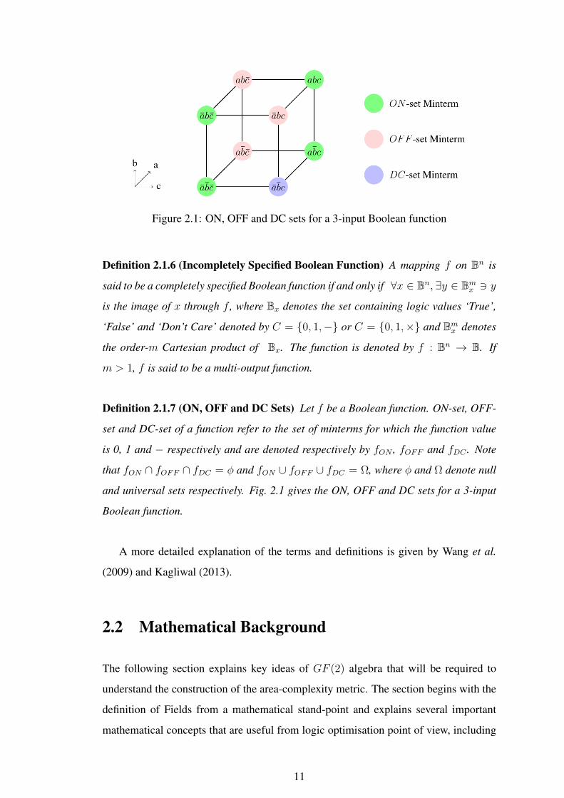
Figure 2.1: ON, OFF and DC sets for a 3-input Boolean function
Definition 2.1.6 (Incompletely Specified Boolean Function) A mapping f on Bn is
said to be a completely specified Boolean function if and only if ∀x ∈ Bn, ∃y ∈ Bmx 3 y
is the image of x through f , where Bx denotes the set containing logic values ‘True’,
‘False’ and ‘Don’t Care’ denoted by C = 0, 1,− or C = 0, 1,× and Bmx denotes
the order-m Cartesian product of Bx. The function is denoted by f : Bn → B. If
m > 1, f is said to be a multi-output function.
Definition 2.1.7 (ON, OFF and DC Sets) Let f be a Boolean function. ON-set, OFF-
set and DC-set of a function refer to the set of minterms for which the function value
is 0, 1 and − respectively and are denoted respectively by fON , fOFF and fDC . Note
that fON ∩ fOFF ∩ fDC = φ and fON ∪ fOFF ∪ fDC = Ω, where φ and Ω denote null
and universal sets respectively. Fig. 2.1 gives the ON, OFF and DC sets for a 3-input
Boolean function.
A more detailed explanation of the terms and definitions is given by Wang et al.
(2009) and Kagliwal (2013).
2.2 Mathematical Background
The following section explains key ideas of GF (2) algebra that will be required to
understand the construction of the area-complexity metric. The section begins with the
definition of Fields from a mathematical stand-point and explains several important
mathematical concepts that are useful from logic optimisation point of view, including
11

co-factor, Shannon’s expansion, Boolean difference, Taylor series and Fourier
Transform for Boolean Cube.
2.2.1 The Concept of a Field
This subsection gives the necessary definitions required to understand and appreciate
the abstract mathematical concept of field. The Galois Field of order 2, in particular,
is of great importance for mathematics pertaining to digital logic. The proposed area-
complexity metric is derived as a result of defining Fourier Transform in GF (2) and
then computed over Boolean Cube. This subsection is for those readers who enjoy
mathematical rigour. Other readers, more interested in the final application of the area-
complexity metric, can skip this subsection.
Definition 2.2.1 (Binary Operation) Let S be a set 3 S 6= φ. A function f : S × S →
S is said to be a binary operation on S
Definition 2.2.2 (Binary Structure) A set S 6= φ, together with a binary operation •
on S is called a binary structure (or just structure) and is denoted by (S, •).
Definition 2.2.3 (Associativity) A binary operation • on set S 6= φ is said to be
associative if and only if ∀a, b, c ∈ S, a • (b • c) = (a • b) • c.
Definition 2.2.4 (Commutativity) Let (S, •) be a structure. The operation • is said to
be commutative if and only if ∀a, b ∈ S, a • b = b • a.
Definition 2.2.5 (Semigroup) A binary structure (S, •) is said to be a semigroup if and
only if • is associative.
Definition 2.2.6 (Identity) Let (S, •) be a structure. An element e ∈ S is said to be an
identity if and only if ∀a ∈ S, a • e = e • a = a.
Definition 2.2.7 (Monoid) A semigroup with an identity is called a monoid.
Definition 2.2.8 (Inverse) Let (S, •) be a monoid. Let a ∈ S. An element a ∈ S is said
to be an inverse of a if and only if a • a = a • a = e.
12

Definition 2.2.9 (Group) A monoid (S, •) is said to be a group if and only if ∀a ∈
S, ∃ a ∈ S 3 a is the inverse of a.
Definition 2.2.10 (Abelian Semigroup) A semigroup (or monoid or group) (S, •) is
said to be Abelian if and only if the operation • is commutative.
Definition 2.2.11 (Rings) A setR together with two binary operations, usually denoted
by • and +, is called a ring if and only if
1. (R,+) is an Abelian group
2. (R, •) is a semigroup and
3. Distributive laws hold. That is, a•(b+c) = a•b+a•c and (a+b)•c = a•c+b•c.
The ring is denoted by (R,+, •).
Definition 2.2.12 (Commutative Ring) A ring (R,+, •) is said to be commutative if
and only if the operation • is commutative.
Definition 2.2.13 (Ring with Unity) A ring (R,+, •) is said to have unity if and only
if (R, •) is a monoid.
Note: Let (R,+, •) be a ring. Usually, + is called addition and • is referred to as
multiplication. (R,+) and (R, •) are said to be additive group and multiplicative
semigroup of (R,+, •). Also, The identity of (R,+) is called additive identity or zero
and is denoted by 0. Similarly, if (R, •) is a monoid, then its identity is called
multiplicative identity or unity and is denoted by 1.
Definition 2.2.14 (Division Ring) Let (R,+, •) be a unity ring. Let R∗ = R \ 0. If
(R∗, •) is a group, then (R,+, •) is called a division ring.
Definition 2.2.15 (Field) A commutative division ring is called a field.
Note: To summarise, a setR together with operations of multiplication and addition
is called a field if and only if
1. Addition and multiplication are closed, associative and commutative
2. There exist additive identity 0 and multiplication identity 1
3. Every element in R has an additive inverse and every non-zero element in R hasa multiplicative inverse.
13

2.2.2 Galois Field and Digital Logic
Definition 2.2.16 (Galois Field) A field (F,+, •) is called Galois Field (also Finite
Field) if and only if |F | ∈ R and |F | is said to be the order of the Galois Field, where
|F | denotes the cardinality of the set F .
Note: The smallest Galois Field is the one with order 2, also denoted by GF (2).
This is also the most popular Galois Field for its application to digital logic. Henceforth,
the generic term Galois Field has been used to refer to the specific field GF (2) that is
of interest from circuits point-of-view.
Definition 2.2.17 (GF(2)) Galois Field of Order 2 (B,+, •) is defined as follows.
+ 0 10 0 11 1 0
• 0 10 0 01 0 1
Table 2.1: Definition of order 2 Galois Field
Properties
1. Addition is equivalent to logical XOR and multiplication is equivalent to logicalAND.
2. Addition and multiplication are closed, commutative and associative. 0 and 1 areadditive and multiplicative identities, respectively.
3. ∀a ∈ B, the element itself is its own additive inverse and also its ownmultiplicative inverse (provided a 6= 0).
Subtraction a − b is defined as addition of a with the additive inverse of b. The
third property above implies that subtraction is the same operation as addition. That
is a − b ≡ a + b ≡ a ⊕ b. Similarly, division a/b can be shown to be equivalent of
multiplication a • b (also denoted simply as ab) provided b 6= 0.
Once the definition and properties ofGF (2) are understood, it is easy to port popular
mathematical tools such as discrete difference, Taylor series and Fourier transform from
the R field to GF (2).
14

2.2.3 Shannon’s Expansion
Definition 2.2.18 (Cofactor) Let f(x1, x2, ..., xk) be a Boolean function. The cofactor
of f with respect to a literal a ∈ xi, xi | i = 1 to k is the Boolean function obtained
when after all instances of a in f are substitutes by logic 1 and all instances of a in f
are substituted by logic 0. Cofactor of f with respect to a is denoted as fa. That is,
fxi= f(x1, x2, ..., xi−1, 1, xi+1, ..., xk) and fxi
= f(x1, x2, ..., xi−1, 0, xi+1, ..., xk)
Let f(x1, x2, ..., xk) be a Boolean function. Then f can be written as
f = xi • fxi+ xi • fxi
3 1 ≤ i ≤ k
This is known as Shannon’s expansion.
2.2.4 Boolean Difference
Boolean difference is the GF (2) equivalent of differentiation of a real-valued function
defined over a continuous domain or difference of a real-valued function defined over a
discrete domain. It is defined simply as real difference computed in GF (2).
Definition 2.2.19 (Boolean Difference) Let f(x1, x2, ..., xk) be a Boolean function.
The Boolean Difference of f with respect to xi, 1 ≤ i ≤ k is defined as
∂f
∂xi=f(xi = 1)− f(xi = 0)
1− 0as computed in GF (2), that is
∂f
∂xi= fxi
⊕ fxi
since both addition and subtraction in GF (2) are equivalent to the logical XOR
operation.
Properties
1. Applying the definition of Boolean difference recursively, we get compute thenth-order partial derivative of f with respect to a variable x as
∂nf
∂xn= f (n−1)
x ⊕ f (n−1)x
15
where f (n) denotes the nth-order partial derivative of f with respect to x. Observethat ∂f
∂x= fx⊕ fxi
is not a function of x, since both fx and fxiare independent of
x. Therefore, ∂2f∂x2 = 0. By Principle of Mathematical Induction, it can be shown
that ∂nf∂xn = 0∀n ∈ N, n ≥ 2.
2. Also notice that ∂f∂x1∂x2
= ∂f∂x1∂x2
= fxixj⊕ fxixj
⊕ fxixj⊕ fxixj
. In general, thepartial derivative of f with respect to m number of variables is simply the logicalXOR of the 2m cofactors obtained by using these literals.
2.2.5 Taylor Series Expansion
Let f(x) be a real-valued function. Taylor series expansion of the function gives
f(x) = f(c) +∞∑k=1
1
k!
∂kf
∂xk
∣∣∣∣x=c
(x− c)k
valid within its radius of convergence. Since the higher order derivatives of a Boolean
function evaluate to zero, Taylor series expansion of Boolean functions is simply
f(x) = f(c)⊕ (fx ⊕ fx)(x⊕ c)
since addition and subtraction operations both correspond to logical XOR in GF (2).
For a multi-variable function, the Taylor series expansion can be obtained by
successively expanding with respect to each of the variables. The final expansion
obtained is symmetric with respect to the input variables and independent of the order
in which expansion is performed. For example, for a two input function, Taylor series
expansion can be obtained as follows. The function is first expanded using Taylor
series with respect x1 and thereafter with respect to x2.
f(x1, x2) = f(c1, x2)⊕ (fx1(c2)⊕ fx1(c2))(x1 ⊕ c1)
= f(c1, c2)⊕ (fx1(c2)⊕ fx1(c2))(x1 ⊕ c1)
⊕ [fx2(c1)⊕ (fx1x2 ⊕ fx1x2)(x1 ⊕ c1)](x2 ⊕ c2)
⊕ [fx2(c1)⊕ (fx1x2 ⊕ fx1x2)(x1 ⊕ c1)](x2 ⊕ c2)
= f(c1, c2)⊕ (x1 ⊕ c1)(fx1(c2)⊕ fx1(c2)) ⊕ (x2 ⊕ c2)(fx2(c1)⊕ fx2(c1))
⊕ (x1 ⊕ c1)(x2 ⊕ c2)(fx1x2 ⊕ fx1x2 ⊕ fx1x2 ⊕ fx1x2)
16

In general the Taylor series expansion for n-input function can be expressed as
follows. Let x, c, i ∈ Bn. Let x = (xb c) ∧b i, where ⊕b represents bitwise XOR
and ∧b represents bitwise AND. Also define
F i(c) =∂F (c)
∂xi11 ∂xi22 ...∂x
inn
where
∂xijj =
1 if ij = 0
xijj if ij = 1
Using the above notation, the Taylor series expansion for a Boolean function about
an arbitrary point c ∈ Bn is given as
F (x) =⊕i ∈ Bn
F i(c) · xi11 · xi22 · ... · xinn
2.2.6 Fourier Transform
Fourier transform on Boolean Cube can be defined as a special case of Discrete Time
Fourier Series (DTFS). Let x be a discrete time signal with periodicity K. DTFS is
defined as follows.
X[s] =1√K
K−1∑k=0
x[k] exp(−2πjks/K)
where j represents square root of −1.
Now consider a single input Boolean function as a signal with input along the
independent axis and the output of the function on the dependent axis. Now compute
DTFS for this signal. Note that in this case K = 2.
X[s] =1√2
1∑k=0
x[k] exp(−πjks) =1√2
1∑k=0
(−1)ks
This is Fourier transform on a 1-D Boolean cube.
Now consider a Boolean function with N inputs and 1 output. Represent the output
as an N -dimensional signal with each of the N inputs along an axis so that the Boolean
function is now represented as a Boolean cube of N dimensions. Computing Fourier
17
transform on this N -dimensional Boolean cube is analogous of N -dimensional DTFS
with K = 2. Therefore, Fourier transform on N -dimensional Boolean cube can be
represented as
X[s] = 2−N/2∑k ∈ Bn
x[k](−1)k·s
where k, s ∈ Bn and k · s represents dot product of the two vectors. This is the general
expression for Fourier transform on Boolean cube.
It is easy to observe that the above equation can be represented in matrix form as
X2n×1 = H2n×2n · x2n×1
where H represents Hadamard matrix of the appropriate size with scaling factor
absorbed, X and x are vectors giving the Fourier coefficients and truth table
respectively, both in lexicographic ordering. Having the Fourier transform in the form
of a simple matrix multiplication is very useful from computation viewpoint.
Note: The way it is defined, Fourier transform and inverse Fourier transform are exactly
identical to each other.
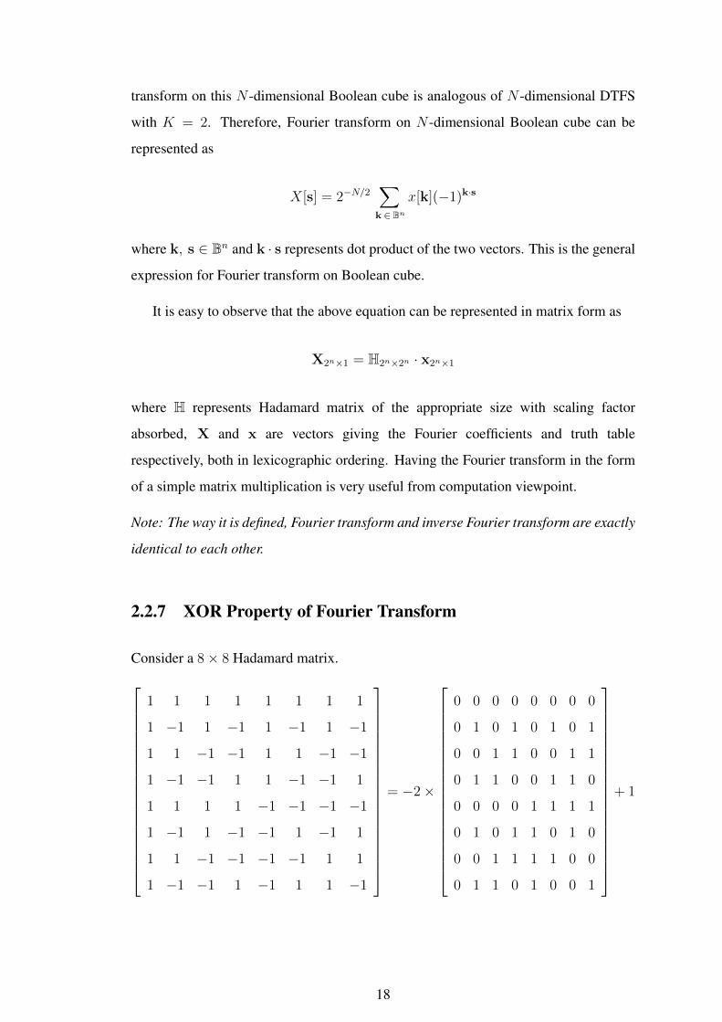
2.2.7 XOR Property of Fourier Transform
Consider a 8× 8 Hadamard matrix.
1 1 1 1 1 1 1 1
1 −1 1 −1 1 −1 1 −1
1 1 −1 −1 1 1 −1 −1
1 −1 −1 1 1 −1 −1 1
1 1 1 1 −1 −1 −1 −1
1 −1 1 −1 −1 1 −1 1
1 1 −1 −1 −1 −1 1 1
1 −1 −1 1 −1 1 1 −1
= −2×
0 0 0 0 0 0 0 0
0 1 0 1 0 1 0 1
0 0 1 1 0 0 1 1
0 1 1 0 0 1 1 0
0 0 0 0 1 1 1 1
0 1 0 1 1 0 1 0
0 0 1 1 1 1 0 0
0 1 1 0 1 0 0 1
+ 1
18

Thus,
H8×8 = −2×
0
c
b
b⊕ c
a
a⊕ c
a⊕ b
a⊕ b⊕ c
+ 1
Each row of the above array represents truth table of an XOR function. Let the array
of XOR truth tables be denoted by h8×8. Thus,
H8×8 = −2× h8×8 + 1
Fourier transform for an n-input function can therefore be expressed as
X2n×1 = 2−n/2 ×H2n×2n × x2n×1 = 2−n/2 −2h2n×2n × x2n×1 + 12n×2n × x2n×1
Note that 1 is a square matrix with all ones and size same as that of h. The above
expression can be simplified as
X2n×1 = 2−n/2 ×
−2×
h01×2n × x2n×1
h11×2n × x2n×1
.
.
.
h2n−11×2n × x2n×1
+ 2n × E[x]
where hi
1×2n are rows of h2n×2n . To make the notation less cumbersome, the subscripts
under matrices indicating their sizes are dropped. On simplifying further
19
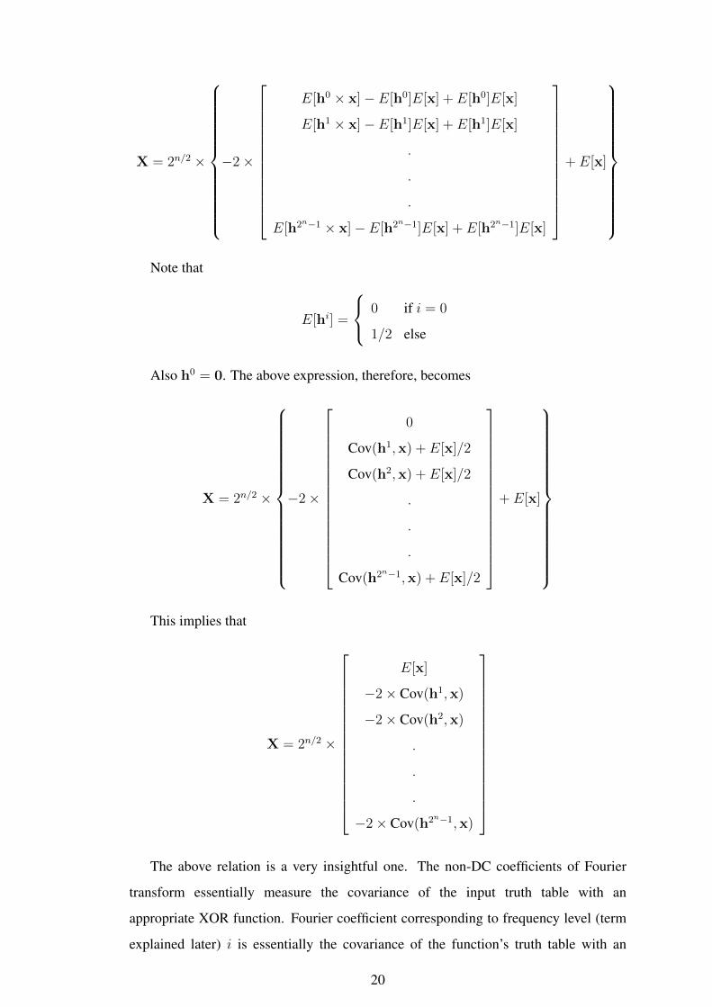
X = 2n/2 ×
−2×
E[h0 × x]− E[h0]E[x] + E[h0]E[x]
E[h1 × x]− E[h1]E[x] + E[h1]E[x]
.
.
.
E[h2n−1 × x]− E[h2n−1]E[x] + E[h2n−1]E[x]
+ E[x]
Note that
E[hi] =
0 if i = 0
1/2 else
Also h0 = 0. The above expression, therefore, becomes
X = 2n/2 ×
−2×
0
Cov(h1,x) + E[x]/2
Cov(h2,x) + E[x]/2
.
.
.
Cov(h2n−1,x) + E[x]/2
+ E[x]
This implies that
X = 2n/2 ×
E[x]
−2× Cov(h1,x)
−2× Cov(h2,x)
.
.
.
−2× Cov(h2n−1,x)
The above relation is a very insightful one. The non-DC coefficients of Fourier
transform essentially measure the covariance of the input truth table with an
appropriate XOR function. Fourier coefficient corresponding to frequency level (term
explained later) i is essentially the covariance of the function’s truth table with an
20

appropriate XOR of i of the n variables. This implies that functions with high energy
in high frequency Fourier coefficients are more "similar" to n-input XOR function and
those with high energy in low frequency Fourier coefficients are more "similar" to an
identically 0 function. Thus, it is only intuitive to expect that functions with higher
energy in high frequency Fourier coefficients are more complex and will require more
area than those functions in which the Fourier energy is concentrated in the lower
frequency regions.
Now consider inverse Fourier transform.
x = H×X =2n−1∑i=0
XiHi
where Hi represents the ith column vector of H. Also,
Hi = 1− 2hi
where hi represents the ith column of h. Implies
x = 2−n/2 ×
2n−1∑i=0
Xi − 22n−1∑i=0
Xihi
Also 2−n/2 × (X0 +X1 + ...+X2n) = x0. Therefore,
x− x0 = 2−n/2 ×
−2
2n−1∑i=0
Xihi
Each hi represents an XOR function of 0 to n of the n variables. Thus, Fourier
transform on Boolean cube is nothing but representing the given truth table as a linear
combination of all possible 2n XOR functions. Thus, higher the magnitude of a
coefficient, higher is the contribution of that specific XOR. It is only natural, therefore,
that functions with Fourier energy concentrated in the higher frequency levels tend to
be more similar to more complex XOR functions and hence occupy more area upon
synthesis and mapping.
As an example, consider the function F (a, b, c) = a + (b ⊕ c). Truth table of
the function is a column vector [0, 1, 1, 0, 1, 1, 1, 1]T . The Fourier coefficients can be
21

computed as the product of this vector with 8× 8 Hadamard matrix.
2−3/2 ×
1 1 1 1 1 1 1 1
1 −1 1 −1 1 −1 1 −1
1 1 −1 −1 1 1 −1 −1
1 −1 −1 1 1 −1 −1 1
1 1 1 1 −1 −1 −1 −1
1 −1 1 −1 −1 1 −1 1
1 1 −1 −1 −1 −1 1 1
1 −1 −1 1 −1 1 1 −1
0
1
1
0
1
1
1
1
= 2−3/2 ×
6
0
0
−2
−2
0
0
−2
The column vector on the right represents the Fourier transform of the function.
E[x] = E[0, 1, 1, 0, 1, 1, 1, 1] = 6/8
Cov(x, b⊕ c) = 1/8× [0, 1, 1, 0, 1, 1, 1, 1][0, 1, 1, 0, 0, 1, 1, 0]T
− E[0, 1, 1, 0, 1, 1, 1, 1]E[0, 1, 1, 0, 0, 1, 1, 0]
= 4/8− 6/8× 4/8 = 1/8
Similarly, it can be shown that Cov(x, a) = 1/8 and Cov(x, a ⊕ b ⊕ c) = 1/8 and all
other covariances are zero.
−23/2 ×
E[x]
−2Cov(x, b)
−2Cov(x, c)
−2Cov(x, b⊕ c)
−2Cov(x, a)
−2Cov(x, a⊕ c)
−2Cov(x, a⊕ b)
−2Cov(x, a⊕ b⊕ c)
=23/2
8×
6
0
0
−2
−2
0
0
−2
= 2−3/2 ×
6
0
0
−2
−2
0
0
−2
= X
which is the same answer computed earlier. Thus, apart from DC component, a +
(b⊕ c) has contribution from (b⊕ c), a and (a⊕ b⊕ c). We can write the given function
22

as a linear combination of these XORs.
0
1
1
0
1
1
1
1
=1
2
0
1
1
0
0
1
1
0
+1
2
0
0
0
0
1
1
1
1
+1
2
0
1
1
0
1
0
0
1
Thus,
a ∨ (b⊕ c) =1
2b⊕ c+
1
2a+
1
2a⊕ b⊕ c
Similarly
a∨ bc =3
4a+
1
4b+
1
4c+
1
4a⊕ b+
1
4a⊕ c − 1
4b⊕ c − 1
4a⊕ b⊕ c
It can be observed that a ∨ bc has contribution mostly from single input XORs,
that is, a, b and c than from more complex XORs. Thus, it is expected that a∨ (b⊕ c)
should be more complex than a∨bc. The prediction is, in fact, true. After synthesising
in SIS, the former requires 3 gates and 8 units of normalised area whereas the latter takes
up 2 gates and 4 units of area.
Thus, circuits with more Fourier area in the higher frequency levels tend to be more
complex than those with energy concentrated in near-DC coefficients.
2.3 Logic Synthesis Packages and Libraries
The following section gives a very brief description of the logic synthesis and
optimization tools and libraries used while working on this project. SIS is the primary
synthesis package used for the project along with MCNC circuit library. The results
were then also verified with Synopsys DC using Nangate 45nm Library to verify the
robustness of the method proposed in this dissertation.
23

2.3.1 SIS
SIS (full form: Sequential Interactive System) is a logic synthesis package developed
in University of California at Berkeley. SIS is an algorithmic sequential circuit
optimization program. SIS starts from a description of a sequential logic macro-cell
and produces an optimized set of logic equations plus latches which preserves the
input-output behaviour of the macro-cell. The sequential circuit can be stored as a
finite state machine or as an implementation consisting of logic gates and memory
elements. The program includes algorithms for minimizing the area required to
implement the logic equations, algorithms for minimizing delay, and a technology
mapping step to map a network into a user-specified cell library. The task of
optimising combinational circuits is a subset of the task of achieving that for
sequential circuits. SIS can, therefore, also be used to optimise combinational circuits,
which is how SIS is used for the purpose of this project. SIS was particularly
well-suited for this project due to its compatibility with BLIF (explained later). More
details about SIS can be found at
http://www.cs.columbia.edu/~cs6861/sis/sis.1.html
2.3.2 Synopsys Design Compiler
Synopsys Design Compiler, popularly known as Synopsys DC, is an RTL synthesis
tool developed by Synopsys, Inc., which optimises designs to provide the smallest and
fastest logical representation of a given function. It comprises tools that synthesise
HDL designs into optimised technology-dependent, gate-level designs. It supports a
wide range of flat and hierarchical design styles and can optimize both combinational
and sequential designs for speed, area and power. More information on Synopsys DC
can be found at http://acms.ucsd.edu/_files/dcug.pdf
2.3.3 MCNC Genlib
MCNC Genlib is a standard cell library of basic logic gates developed at
Microelectronics Center of North Carolina (MCNC). It consists of a total of 22 gates.
MCNC homepage can be accessed at https://www.mcnc.org/ and MCNC
24
Genlib can be found at http:
//www.cs.ucla.edu/classes/layout/misII/lib/mcnc.genlib
2.3.4 NanGate 45nm Library
The NanGate 45nm Open Cell Library (also known as NanGate 45nm Library) is an
open-source, standard-cell library provided for the purposes of testing and exploring
EDA flows. NanGate developed and donated this library to Si2.org for open use. The
library is intended to aid university research programs and organizations such as Si2 in
developing flows, developing circuits and exercising new algorithms. More information
can be found at http://www.nangate.com/
2.3.5 BLIF Circuit Specification Format
BLIF stands for Berkeley Logic Interchange Format. The goal of BLIF is to describe a
logic-level hierarchical circuit in textual form. A circuit is an arbitrary combinational
or sequential network of logic functions. A circuit can be viewed as a directed graph of
combinational logic nodes and sequential logic elements. Each node has a two-level,
single-output logic function associated with it. Each feedback loop must contain at
least one latch. Each net (or signal) has only a single driver, and either the signal or the
gate which drives the signal can be named without ambiguity. BLIF was particularly
well-suited for this project since it is easy to switch back and forth between BLIF and
truth table format, which is convenient for computing Fourier transform. A detailed
description of BLIF can be found at http:
//www.cs.uic.edu/~jlillis/courses/cs594/spring05/blif.pdf
25

CHAPTER 3
AREA COMPLEXITY USING FOURIER
TRANSFORM
Estimation of logic area required by a combinational design is useful across several
stages of high level and logic synthesis. The final silicon footprint of a chip comprises
logic, routing and other global resources. Estimation of the logic area required at earlier
stages in the design process has been done widely in practice. Area-complexity of
a circuit refers to the area required by the logic portion of the combinational design
without performing technology mapping.
3.1 Basic Idea
Several attempts have been made in the past to capture the area requirements of circuits
without performing technology mapping. One of the simplest heuristics that have been
used in the past is the fraction (F ) of minterms covered by a function. In general, if F
is close to 0.5, the function is expected to be more complex than those which are near
tautology or antithesis. For example, an XOR gate, which has an equal number of 1’s
and 0’s is much more complex than an AND gate which is a bit away from antithesis.
However, it’s not hard to observe that the minterm fraction heuristic fails miserably
in several very obvious cases. For example, an XOR gate, a simple inverter and a
buffer, all have equal number of 1’s and 0’s, but they are as drastically different in
terms of complexity as they possibly could be. This example demonstrates that it’s
not the number of 1’s and 0’s, but rather their placement in the truth table is what is
deterministic of the area requirement of a Boolean function.
Moreover, a function that depends on more number of its inputs takes up more area
upon synthesis than a function that depends on all of its inputs. For example, in a
NOR gate, knowing that any one input is 1 is sufficient to determine the output without
knowing the logical state of the remaining inputs. As against this, to determine the
output or an XOR gate, it is required to know all of its inputs. Thus, the dependence of
output of a NOR gate on its inputs is "weaker" than that for XOR or XNOR gate. Thus,
the nature of dependence of the output on each of its inputs is important in capturing
the area requirement of circuits mathematically.
Both, the location of 1’s and 0’s in a truth table as well as the strength of
dependence of the function output on each of its inputs is captured very effectively by
Fourier transform computed on the truth table Boolean cube of the function.
Function Minterms Fourier Energy in Different Freq. Levels Area GateF (a, b, c) Covered Freq. Level 3 Freq. Level 2 Freq. Level 1 Count
a 4 0 0 2 0 0a+ b 6 0 0.5 1 3 1abc 1 0.125 0.375 0.375 4 2
a(b+ c) 3 0.125 0.375 1.375 4 2a(b⊕ c) 2 0.5 0.5 0.5 8 3a⊕ b⊕ c 4 2 0 0 10 2
Table 3.1: Effectiveness of minterm cover heuristic and Fourier energy distribution inestimating area complexity ordering of combinational circuits
In the table above, six different 3-input functions are listed. For each function
Fourier transform is computed. The Fourier energy is then classified into 3 frequency
levels. This part is explained later in this section. Level 3 corresponds to highest
frequency level and is analogous to high frequency terms in the conventional Fourier
transform. It is demonstrated through this table that Fourier energy distribution is very
effective is comparing area requirement between circuits. To estimate area requirement
comparison between two circuits, compare the Fourier energy in different levels in a
switch-case manner giving higher priority to higher frequency levels. It can be seen
that the proposed metric is much more effective as compared to using the fraction of
minterms covered.
3.1.1 Frequency Levels
Given a Boolean function with N inputs, Fourier transform is computed on the
corresponding N -dimensional Boolean cube. The output of the Fourier transform is
another Boolean cube, again with N dimensions. Each vertex of this cube represents a
Fourier coefficient. Classify the Fourier coefficients using Hamming distance of the
27

Figure 3.1: Frequency Levels for a 3-dimensional Boolean Cube
vertices from the origin, 0, of the Fourier cube. The Hamming distance can range
between 0 and N . The coefficients are thus grouped into N + 1 classes. 0 corresponds
to DC component and 1 corresponds to highest frequency. In general, higher
Hamming distance is analogous to higher frequency. Each of the classes are termed, in
this dissertation, as Frequency Levels, labelled as per Hamming distance from origin.
Level 0, thus, represents DC and higher level number is analogous to higher frequency.
Functions with high energy distribution in the higher frequency levels tend to be more
"similar" to complex XOR function and hence are intuitively expected to take up more
area. Similarly, those with large energy in lower frequency levels tend to be "similar"
to XORs of fewer number of variables and hence are less complex.
The above image shows the frequency levels on a Fourier cube obtained as a result
of Fourier transform on a function with 3 inputs. Frequency levels 0, 1, 2 and 3 are
indicated based on Hamming distance of a vertex from the origin, in the Fourier cube.
Level 3 is analogous to high frequency term and level 0 represents DC component. Next
to each vertex, an XOR equation is listed in black. The Fourier transform coefficient at a
vertex represents how similar the input truth table is to that corresponding XOR. Higher
the magnitude of a Fourier coefficient, higher is the contribution of the corresponding
XOR in obtaining the truth table of the given function. As a result, Fourier transform
of an XOR function will give non-zero Fourier coefficients only for DC component and
the vertex corresponding to that XOR in the Fourier cube.
28
Area-complexity analysis is required in mainly two classes of problems: (i) Finding
the most area-efficient circuit from a set of circuits and (ii) Given a circuit, getting an
estimate of its area requirement and gate count. These two types of problems will be
discussed in detail in this chapter. The supporting experiments and results are presented
in the next chapter.
3.2 Problem Type 1: Identifying Optimum Circuit
Given a set of circuits, it is required to find that circuit or set of circuits, which occupy
the least possible area, while retaining the required functionality. This problem is
commonly encountered due to inherent flexibility in the task at hand which leads to
flexible functionality specification. A common example is existence of don’t care
terms. Another application is in the field of approximate computing. Due to inherent
forgiving nature of the problem, self-healing algorithms, noisy inputs or error tolerant
codes, it is possible to design circuits which give outputs within a permissible
tolerance and using this flexibility to optimise for area and power. This include
applications where the final output is evaluated collectively by a human sensory organ.
Common examples are speech, audio, video, image processing, decision-making
algorithms which compare the output to a set of thresholds and thus the exact value of
the output is not relevant etc. In both, don’t care considerations and designing
approximate circuits, the problem essentially boiled down to a set of circuits which
satisfy the given don’t care constraint or given error tolerance limit and finding that
subset which is optimum in terms of area and / or power.
The following algorithm can be used to design approximate circuits using the
proposed area-complexity metric. In the algorithm, even though the set S of all circuits
that satisfy the specified constraints can be potentially very large, in each iteration only
the required coefficients are computed and that too only for the required subset of
circuits. Therefore, despite the large size of initial set S, the algorithm can be run in
reasonable amount of time. The same algorithm is also depicted as a flow chart in
Fig. 3.2
29
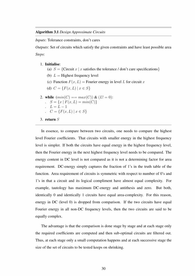
Algorithm 3.1 Design Approximate Circuits
Inputs: Tolerance constraints, don’t cares
Outputs: Set of circuits which satisfy the given constraints and have least possible area
Steps:
1. Initialise:(a) S = Circuit x | x satisfies the tolerance / don’t care specifications(b) L = Highest frequency level
(c) Function F (x, L) = Fourier energy in level L for circuit x
(d) C = F (x, L) | x ∈ S
2. while (min(C) == max(C)) & (L! = 0):. S = x | F (x, L) = min(C). L = L− 1. C = F (x, L) | x ∈ S
3. return S
In essence, to compare between two circuits, one needs to compare the highest
level Fourier coefficients. That circuits with smaller energy in the highest frequency
level is simpler. If both the circuits have equal energy in the highest frequency level,
then the Fourier energy in the next highest frequency level needs to be compared. The
energy content in DC level is not compared as it is not a determining factor for area
requirement. DC-energy simply captures the fraction of 1’s in the truth table of the
function. Area requirement of circuits is symmetric with respect to number of 0’s and
1’s in that a circuit and its logical compliment have almost equal complexity. For
example, tautology has maximum DC-energy and antithesis and zero. But both,
identically 0 and identically 1 circuits have equal area-complexity. For this reason,
energy in DC (level 0) is dropped from comparison. If the two circuits have equal
Fourier energy in all non-DC frequency levels, then the two circuits are said to be
equally complex.
The advantage is that the comparison is done stage by stage and at each stage only
the required coefficients are computed and then sub-optimal circuits are filtered out.
Thus, at each stage only a small computation happens and at each successive stage the
size of the set of circuits to be tested keeps on shrinking.
30
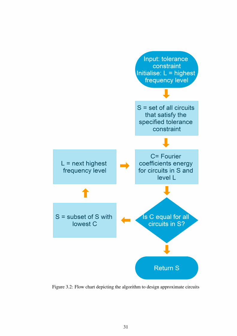
Figure 3.2: Flow chart depicting the algorithm to design approximate circuits
31

3.3 Problem Type 2: Estimating the Area and Gate
Count
In several circuit design applications, it is required to obtain an estimate, at least a
rough one, of how much area the circuit will occupy when it is actually implemented
on a Silicon chip. One method is to perform synthesis and mapping on the design
specification and get an estimate of the area requirement from the mapping report.
This method, however, is computationally taxing and time consuming. Using the
proposed area-complexity metric, it is possible to get a reasonable estimate of the
post-mapping area using only mathematical and statistical analysis. Obtaining area
estimate using Fourier energy distribution poses a significantly smaller computing
effort when compared to the traditional approach.
Area estimate can be obtained by using linear combination of Fourier energy
content in the non-DC frequency levels. The weights for frequency levels can be
determined using regression analysis. Regression analysis captures the characteristics
of the technology in which the circuit is to be finally implemented.
M =n∑
i=1
wiei
where ei is the net Fourier energy, of the circuit under consideration, in the ith
frequency level. For n-input circuit, there are n frequency levels apart from DC (level
0). The energy content in DC level is not important to determine the area requirement
of circuits. DC energy simply gives a measure of the fraction of 1’s in the truth table of
the function. However, a function and its logical negation, have almost equal area
requirement and thus it is clear that DC-energy of a function does not play role in
deciding area-complexity. Notice that index zero is dropped from the summation. wi is
the weight for frequency level i in the linear combination. The wi’s are determined
using regression on a large number of circuits with known area in the required
technology.
Even though regression can be time consuming, it is a one time effort. For a given
technology, regression coefficients can be stored in a lookup table to be used for area
estimation later. Results are discussed in the next chapter.
32

3.4 Multi-Output Circuits
All of the analysis discussed so far can be performed on a truth table and hence, by
default, is applicable only to single-output circuits. Extending this metric to multiple
outputs can’t be done by simply adding together the area prediction for each of the
individual outputs due to the phenomenon of resource-sharing. Certain logic blocks
can be shared between two or more of the outputs and thus, simply adding together the
area requirement for each individual output will lead to gross over-prediction of the net
area requirement of the circuit as a whole. Therefore, it is necessary to capture possible
sharing of resources between outputs of the circuit and then predict the area that the
circuit will occupy after correcting for this sharing.
Since throughout this project, effort has been made to capture hardness of the
circuits mathematically rather than using synthesis tools, a couple of methods have
been tried out to estimate possible resource-sharing. The methods are (i) computing
XORs of outputs and (ii) computing correlation between outputs.
For a circuit with 2 outputs
A = A1 + A2 − ρmin(A1, A2)
where A represents the net area of the whole circuit. A1 and A2 are individual area
requirements of outputs 1 and 2, respectively. ρ represents Sharing Coefficient, 0 ≤
ρ ≤ 1. Thus, minimum sharing is 0 when ρ = 0 and maximum sharing is min(A1, A2)
when ρ = 1. Taking minimum of the individual output areas makes sense because this
is the maximum sharing that can occur (when one of the outputs is used to later derive
the other output).
Two different approaches were tried to compute ρ. First is
ρ = Area(Y1 ⊕ Y2)/min(A1, A2), where Yi represent output truth tables. The logic
behind defining sharing like this is that XOR between two outputs captures how
"similar" the two output truth tables are. More similar the truth tables, higher the
possibility for sharing. The other way of capturing similarity between output truth
tables is using correlation. ρ = |Cov(Y1, Y2)| /σY1σY2 , where Cov() represents
covariance and σYirepresents standard deviation of the output truth table. In short, ρ is
nothing but the modulus of the coefficient of correlation between the output truth
33
tables.
For more than two outputs, the sharing can be defined in a fashion analogous to
Inclusion Exclusion Principle.
A =∑
i∈Bm,i6=0
(−1)
m∑j=1
ijρi min
j3ij=1(Aj)
where m is the number of outputs, i = (i1, i2, ..., im) 3 ij ∈ B and ρi is defined over all
outputs Yj for which ij = 1 as
ρ = Area
⊕j3ij=1
Yj
/ minj3ij=1
(Aj)
or
ρ = Cov(Yj | ij = 1)/∏
j3ij=1
σYj
Note: It was found that sharing coefficients defined using correlation are more effective
than those defined using XORs of output truth tables. Hence, throughout this project,
sharing coefficients are defined as correlation coefficients between output truth tables.
34
CHAPTER 4
RESULTS: METRIC ACCURACY AND TIMING
PERFORMANCE
4.1 Methodology
To evaluate the effectiveness of the proposed metric, it was tested with a large collection
of randomly generated circuits with varying inputs and outputs. The following steps
were used to test the metric.
First off, number of inputs and number of outputs were fixed. With these
specifications, a large collection of truth tables was generated randomly. The randomly
generated circuits were then divided into training and test data. Fourier coefficients
were computed on all circuits and the obtained coefficients were then classified into
different frequency levels and the Fourier energy distribution across frequency levels
was computed for each output of each circuit. Secondly, correlation coefficients were
computed analogous to Inclusion-Exclusion principle and these were used to
determine sharing between the outputs of the same circuit.
In parallel, all the generated truth tables were converted into BLIF format and then
run through SIS and area and gate-count were obtained. These values of area and
gate-count, along with Fourier energy distribution and sharing coefficients were used
to train regression coefficients. These coefficients were then used as weights to linearly
combine Fourier energy content in different frequency levels for test data. The area
and gate-count, thus predicted for test data, are then compared against the values
obtained using SIS and error analysis was performed and results were documented.
4.2 Accuracy of Predicted Area
To determine accuracy of the proposed metric, the area and gate count predicted by the
metric was compared with the values obtained using Berkeley SIS synthesis package

with MCNC Library. The metric was also tested against results obtained using
Synopsys DC with 45nm NanGate Library.
Figure 4.1: Ordering of 128 3-input circuits based on predicted hardness using allFourier coefficients (left) and using only highest two frequency levels(right). X-axis represents an abstract complexity measure computed fromFourier coefficients without using regression and Y-axis contains the actualarea post synthesis and mapping.
In Fig. 4.1, area-complexity count (X-axis) has been obtained Fourier coefficients
without using regression. Regression is not required here since we are only interested
in ordering the circuits based on hardness and not in the actual values of area or
gate-count. It can be seen from the graphs that the proposed method is reasonably
successful in ordering circuits correctly based on area which they would occupy after
implementation. Also, notice that there is almost no degradation in correctness of the
sorting even when only the highest 2 frequency levels are used. Computing Fourier
coefficients only in the top 2 frequency levels is less taxing than computing full
Fourier transform.
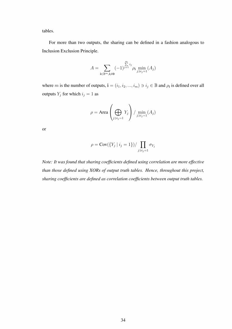
Fig. 4.2represents classification of circuits based only on the highest frequency
coefficient. It can be seen that the classification is successful in dividing the circuits
into course clusters which still give a rough idea about the hardness and area
requirement. Note that this classification is obtained with as less computation as
calculating a single coefficient of Fourier transform. In the figure, class 0 is predicted
to have least area requirement while class 4 is expected to occupy largest area. It can
be seen that the estimation is generally correct except class 4, which is a singleton
class containing XOR of all inputs.
For the problem of area and gate-count estimation, one thousand truth tables for
36
Figure 4.2: Classification of 128 3-input circuits, based only on the highest frequencycoefficient of Fourier transform. X-axis represents abstract area-complexitymetric computed using all Fourier coefficients and Y-axis gives the actualarea post synthesis. The clusters marked on the graph are obtained usingonly the highest frequency coefficient. Notice that using only this onecoefficient, it is possible to classify circuits into rough groups based on theirhardness and area-requirement.
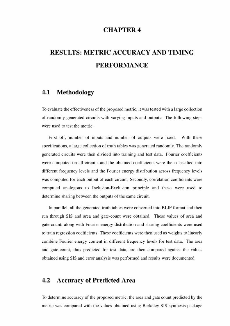
10 input 1 output functions were generated and were used as training data to obtaining
weights for different frequency levels. The Fourier energy content in these different
frequency levels was then linearly combined using these weights to obtain a prediction
on area and gate-count. The predictions were obtained and tested for test data which
consisted of 1000 randomly generated circuits, separate from training data. Visually, it
can be seen from Fig. 4.3 that the data points lie close to the green “X=Y” line.
Figure 4.3: Predicted versus actual area (left) and gate-count (right) for 1000 randomlygenerated 10 input, 1 output circuits. Blue points represent data and thegreen line represents is “X=Y”.
Fig. 4.4 demonstrates working of the proposed metric using the concept of resource
sharing determined using correlation between output truth tables in inclusion-exclusion
37

Figure 4.4: Predicted versus actual area (left) and gate-count (right) for 400 randomlygenerated 10 input, 4 output circuits. Blue points represent data and thegreen line represents “X=Y”.
fashion.
For each data point, absolute error is computed as arithmetic difference between the
predicted and actual value.
Absolute Error = Predicted Value− Actual Value
Relative Error =Predicted Value− Actual Value
Actual Value
Standard deviation is computed for each data point and then standard deviation of
relative error is computed and this value plotted as a function of varying number of
inputs and outputs is represented in Fig. 4.5.
Figure 4.5: Standard deviation of relative error for varying number of inputs (left) andoutputs (right). The blue line displays relative error for gate-count and thegreen line gives that for predicted area.
38

Notice that as size of the circuit increases, the relative error keeps on decreasing.
Most practical circuits are much larger in size than the circuits used in this project to test
the error performance of the proposed metric. This means that the predictions given by
this metric will be more accurate for practical applications than what is demonstrated in
this dissertation. It can be seen that for moderately large circuits, with 10 or more inputs
and more than 4 outputs, the predicted area is within 5% of the actual area considering
3-sigma deviation. For large circuits used in practice, the prediction is expected to be
accurate within a few percent. Thus, the proposed metric gives area predictions with
a very good accuracy and pose a substantially smaller computing effort as compared to
conventional logic synthesis.
4.3 Timing Performance of the Proposed Metric
Figure 4.6: The graph shows the computational time required for processing 1500randomly generated circuits for varying number of outputs (left). Thegraph (right) shows the average computation time required for processing1 circuit, averaged over 2000 randomly generated circuits. The greenline represents the time taken by the traditional method and the blue linerepresents the time taken by the proposed approach.
A major advantage of area-complexity estimation using the proposed metric is that
results accurate within a few percent error are obtained with relatively tiny
computational effort. To demonstrate the computational complexity posed by the
proposed approach as compared to the that posed by the traditional method,
computational time required to process 1000+ randomly generated circuits was
measured. 1000+ circuits each were generated for varying number of inputs and
outputs.
39
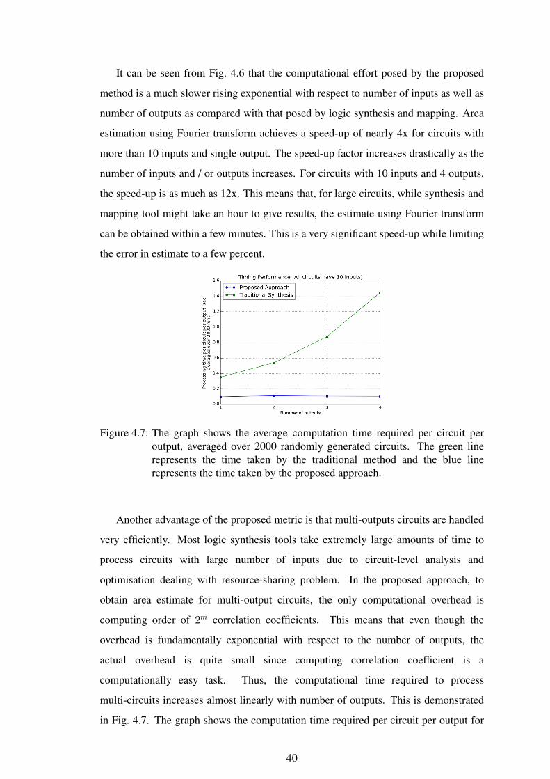
It can be seen from Fig. 4.6 that the computational effort posed by the proposed
method is a much slower rising exponential with respect to number of inputs as well as
number of outputs as compared with that posed by logic synthesis and mapping. Area
estimation using Fourier transform achieves a speed-up of nearly 4x for circuits with
more than 10 inputs and single output. The speed-up factor increases drastically as the
number of inputs and / or outputs increases. For circuits with 10 inputs and 4 outputs,
the speed-up is as much as 12x. This means that, for large circuits, while synthesis and
mapping tool might take an hour to give results, the estimate using Fourier transform
can be obtained within a few minutes. This is a very significant speed-up while limiting
the error in estimate to a few percent.
Figure 4.7: The graph shows the average computation time required per circuit peroutput, averaged over 2000 randomly generated circuits. The green linerepresents the time taken by the traditional method and the blue linerepresents the time taken by the proposed approach.
Another advantage of the proposed metric is that multi-outputs circuits are handled
very efficiently. Most logic synthesis tools take extremely large amounts of time to
process circuits with large number of inputs due to circuit-level analysis and
optimisation dealing with resource-sharing problem. In the proposed approach, to
obtain area estimate for multi-output circuits, the only computational overhead is
computing order of 2m correlation coefficients. This means that even though the
overhead is fundamentally exponential with respect to the number of outputs, the
actual overhead is quite small since computing correlation coefficient is a
computationally easy task. Thus, the computational time required to process
multi-circuits increases almost linearly with number of outputs. This is demonstrated
in Fig. 4.7. The graph shows the computation time required per circuit per output for
40
multi-output circuits. It can be seen that while the time taken by synthesis tool
increases exponentially, that taken by the proposed method is almost constant. This
shows that the computational overhead due to resource-sharing in multi-output circuits
is very small for the proposed metric.
41
CHAPTER 5
CONCLUSION AND FUTURE WORK
5.1 Summary of Results
A novel method for estimating area requirement of combinational circuits is presented
in this dissertation. The advantage of the proposed approach is that it captures the
inherent hardness of the Boolean function purely mathematically. Thus, using Fourier
transform, we can compare Boolean functions with respect to their inherent hardness
while being agnostic to variations introduced in synthesis tools by technology and
optimisation techniques.
Predictions of area and gate-count using the proposed metric is accurate within 5%
for circuits with 10 or more inputs and more than 4 outputs. As the number of inputs and
/ or outputs increases, the percentage error on the prediction goes on reducing. This is
because, as the circuit size increases the absolute error on area and gate-count increases
much slower than the said quantities. This means that for practical application, in which
circuits tend to be large in size, the performance of the metric will be even better than
what is demonstrated here. For most practical circuits, the area prediction is expected
to be accurate within a few percent based on 3-sigma deviation of relative error.
Finally, since the Fourier transform computation is nothing but a simple matrix
operation, the computational complexity posed by this method is very small. Also, the
entire algorithm has been implemented in Python, which is readily and freely available
on almost any machine and operating system. This is another advantage over elaborate
synthesis tools which are often proprietary, work only on certain operating system
platforms and require separate installation. The proposed method achieves a speed-up
of about 4x for predicting area and gate-count single output circuits with 10 or more
inputs as compared to synthesis tools. Also, the computational complexity of this
metric is a much slower rising exponential with respect to number of inputs and
outputs as compared to that for the traditional electronic design flow. For circuits with
10 or more inputs and more than 4 outputs, the speed-up is as much as 12x. As circuit

size increases, the speed-up factor also increases. For most practical circuits, the
proposed algorithm will take only 1/15th the amount of time or smaller as compared to
logic synthesis. This means that, while a design tool might need to run for an hour to
give area requirement, this algorithm can give a very accurate estimate on area
requirement within a few minutes.
This method is very effective in ordering a given set of circuits in the order of
their area requirement. However, to predict the exact area that a circuit will occupy,
one needs to capture the characteristics of the technology in which the circuit is to
be manufactured. Similarly, the gate-count of the circuit will depend on the mapping
library to be used. Hence, to predict area and gate-count of a circuit, in addition to the
Fourier coefficients, regression needs to be used to assign weights to different frequency
levels. These weights capture the features of mapping library and of the technology to
be used. Although regression can be time consuming, it is a one time effort for the said
technology and gate library. Regression coefficients may be computed in advance and
stored in a lookup table for future reference.
Using only the coefficients in the highest few frequency levels, it is possible to
classify circuits into broad families based on their area-complexity. For example, all
input AND-family, all input XOR-family, family of circuits which are independent of
at least one of the inputs, all input AND-XOR combination family etc. get differentiated
using only the highest frequency Fourier coefficient alone. Thus, for a course ranking
of circuits, it is not even required to compute the entire Fourier transform.
Thus, the proposed metric is effective in comparing hardness between circuits as
well as predicting area requirement of circuits in a very small amount of time. Since,
the computational complexity for comparing between circuits is so small, this approach
can also be used to design approximate circuits by comparing and finding the optimum
circuit from a large set of acceptable circuits.
43

5.2 Future Work
The proposed metric and analysis is area-centric. Similar efforts can be made to see
if there is a relation between Fourier energy distribution and power consumption of
combinational circuits and to see whether it will be possible to compare circuits based
on power consumption and even predict power consumption purely mathematically.
The analysis done in this project can also be extended to sequential circuits, by
analysing separately, the combinational blobs between every two flip flops.
To estimate area-complexity of multi-output circuits, correlation coefficients are
computed in Inclusion-Exclusion fashion. This computation is fundamentally
exponential in nature. It should be possible to use only the first few levels of
correlation to effectively estimate sharing since joint correlation between variables is
expected to go closer to zero as the number of variables increases. If this is achieved,
the computational complexity of the algorithm will no longer depend exponentially on
number of outputs.
An effort can also be made to combine Fourier theory discussion in this dissertation
with approximate design technique SALSA, described in Venkataramani et al. (2012)
to develop an approximation technique that will retain the sophistication of SALSA and
achieve the speed-up demonstrated by the proposed approach for area estimation.
Finally, it will be helpful to study Fourier transform on circuits from a more
computer science theory and information theory viewpoint to get a more fundamental
understanding of hardness of Boolean functions.
44

REFERENCES
1. Beg, A. and P. P. C. (2010). Prediction of area and length complexity measures forbinary decision diagrams. Expert Systems with Applications, 37(4), 2864–2873.
2. Cheng, K. T. and V. D. Agarwal, An entropy measure for the complexity of multi-output boolean functions. In In Proceedings of the 27th ACM/IEEE Design AutomationConference, DAC ’90. ACM, New York, NY, USA, 1990.
3. Cook, R. W. (1973). Logical network cost and entropy. Computers, IRE Transactionson, C-22(9), 823–826.
4. de Wolf, R., A Brief Introduction to Fourier Analysis on the Boolean Cube. Number 1in Graduate Surveys. Theory of Computing Library, 2008. URL http://www.theoryofcomputing.org/library.html.
5. Drechsler, R. and D. Sieling (2001). Binary decision diagrams in theory and practice.International Journal on Software Tools for Technology Transfer, 3, 112–136.
6. Kagliwal, A. (2013). Set-Cover Heuristics and Measure of Area-Complexity in LogicSynthesis. Master’s thesis, Department of Computer Science & Engineering, IIT-Madras, Chennai – 600036.
7. Kagliwal, A. and S. Balachandran, Measuring area-complexity using booleandifference. In VLSI Design and 2013 12th International Conference on EmbeddedSystems (VLSID), 2013 26th International Conference on. VLSID, 2013.
8. Kravets, V. N. and P. Kudva, Understanding metrics in logic synthesis for routabilityenhancement. In Proceedings of the 2003 International Workshop on System-levelInterconnect Prediction, SLIP ’03. ACM, New York, NY, USA, 2003. ISBN 1-58113-627-7. URL http://doi.acm.org/10.1145/639929.639931.
9. Kurdahi, F. J. (1993). Linking register-transfer and physical levels of design. IEICETransactions on Information and Systems, 76(9), 991–1002.
10. Muller, D. E. (1956). Complexity in electronic switching circuits. ElectronicComputers, IRE Transactions on, EC-5(1), 15–19.
11. Nemani, M. and F. N. Najm, High-level power estimation and the area complexity ofboolean functions. In High-level power estimation and the area complexity of Booleanfunctions. 1996.
12. Nemani, M., F. N. Najm, and S. Member (1999). High-level area and powerestimation for vlsi circuits. IEEE Trans. Computer-Aided Design, 18, 697–713.
13. Pippenger, N. (1976). Information theory and the complexity of boolean functions.Mathematical Systems Theory, 10(1), 129–167.
14. Raseen, M., P. W. C. Prasad, and A. Assi (2006). An efficient estimation of the robdd’scomplexity. Integr. VLSI Journal, 39(3), 211–228.
45

15. Shannon, C. E. (1949). The synthesis of two-terminal switching circuits. Bell SystemsTechnical Journal, 28, 59–98.
16. Venkataramani, S., A. Sabne, V. Kozhikkottu, K. Roy, and A. Raghunathan, Salsa:Systematic logic synthesis of approximate circuits. In Design Automation Conference(DAC), 2012 49th ACM/EDAC/IEEE. 2012.
17. Wang, L. T., Y. W. Chang, and C. K. T., Electronic Design Automation Synthesis,Verification, and Test. Morgan Kaufmann Publishers, 2009, first edition.
18. Wu, A. H., V. Chaiyakul, and D. Gajski, Layout-area models for high-level synthesis.In In 1991 IEEE International Conference on Computer-Aided Design. ICCAD-91.Digest of Technical Papers 1991, 1991.
46