applications of synchrotron radiation to nano materials ... · applications of synchrotron...
TRANSCRIPT

Applications of Synchrotron Radiation to Nano Materials Science: Activities in East Asia
Keisuke KobayashiNIMS Beamline Station at SPring-8
National Institute for Materials Science
New Subaru
SPring-8
RUSRC
Saga LS
HiSOR
BSRF
HLS
SSRF
NSRRC
SPS
PLS
SSRLS
UVSOR II
Photon Factory

Synchrotron Radiation Facilities in Asia
Ring Energy (GeV)
SSLS PLS SSRFNSSRC SPring-8
New Subaru
1 10 100 1000 10 k 100 k
1000 kPhoton Energy (eV)
0.1
HiSORRUSRC PF
Saga SLS
SPS
UVSOR II

Nano Activies at SPring-8
User Support by the Common Use of Limited and Large-scaled Experimental Facilities
1. HV-TEM2. Nano Foundries3. Synchrotron Radiation4. Mol. Synthesis and Analysis
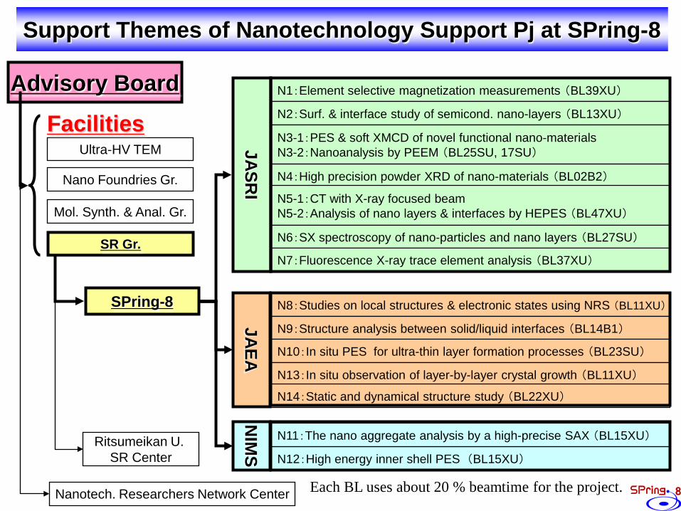
Nanotechnology Support Project involving JASRI, JAEA, and NIMS at SPring-8
April 2002-March 2007
To continue the support to nanotechnology researchers at SPring-8, JASRI has started the new “Nanotechnology Support Program” ,as a priority project of strategic significance that is expected to produce excellent research results. JAEA and NIM has started the same support in the framework of “Nanowet Support Project”.

SR Gr.
Advisory Board
Support Themes of Nanotechnology Support Pj at SPring-8
Ultra-HV TEM
Nano Foundries Gr.
Mol. Synth. & Anal. Gr.
Nanotech. Researchers Network Center
Ritsumeikan U. SR Center
SPring-8
N1:Element selective magnetization measurements (BL39XU)
N2:Surf. & interface study of semicond. nano-layers (BL13XU)
N3-1:PES & soft XMCD of novel functional nano-materials N3-2:Nanoanalysis by PEEM (BL25SU, 17SU)
N4:High precision powder XRD of nano-materials (BL02B2)
N5-1:CT with X-ray focused beamN5-2:Analysis of nano layers & interfaces by HEPES (BL47XU)
N6:SX spectroscopy of nano-particles and nano layers (BL27SU)
N7:Fluorescence X-ray trace element analysis (BL37XU)
N8:Studies on local structures & electronic states using NRS (BL11XU)
N9:Structure analysis between solid/liquid interfaces (BL14B1)
N10:In situ PES for ultra-thin layer formation processes (BL23SU)
N13:In situ observation of layer-by-layer crystal growth (BL11XU)
N14:Static and dynamical structure study (BL22XU)
N12:High energy inner shell PES (BL15XU)
N11:The nano aggregate analysis by a high-precise SAX (BL15XU)JASR
IJAEA
NIM
S
Facilities
Each BL uses about 20 % beamtime for the project.

Energy Devices and Materials
11%
ULSI Tech.13%
Compound Semiconductors
2%
Optical Storage Devices
4%Magnetic
Properties22%
Oxide Electronics1%
Environment6%
New Materials,Surfaces, Interfac
es, and Nano-structurs
10%
Methods and Instrumantions
31%
Electric and Magntic
Properties40%
Total: 481 Proposals (5 years)
Industry8%
National and
Public Research Inst.11%
University
78%
Foreign3%
Research Fields and User Affiliation
75
47
8
79
47
2
87
36
4
51
32
4
68
33
10
87
37
10
81
34
5
80
46
15
84
36
5
0
20
40
60
80
100
Num
ber
of
Pro
posals
02B 03A 03B 04A 04B 05A 05B 06A 06B
Harf-year Research Term
Received
SelectedSelected (new users)

Publications
Journal name Number
Nature 1
Science 1
Surface Science Report 1
Nature Materials 2
Angewandte Chemie International Edition 3
Nano Letters 1
Physical Review Letters 2
Journal of the American Chemical Society 2
Applied Physics Letters 11
Chemical Communications 2
Journal of Physical Chemistry B 2
Physical Review B 18
Chemical Physics Letters 6
Journal of Applied Physics 4
Others 95
Total 151
2
18
36
48 47
0
20
40
60
80
Num
ber o
f Pub
licat
ion
2002 2003 2004 2005 2006/2007
Published Year
20022003200420052006/2007
List of Published JournalsNumber of Refereed Publications

Highlight (Gas Storages)
Gas Adsorption in Metal-Organic Microporus Materials(Nature, Science, Angewandte Int. Edit., S. Kimtagawa et al. (Kyoto Univ.))
O2 Molecules in MOMM[Science 298, 2358 (2002)]
H2 Molecules in MOMM[Angewandte Chemie 44, 920 (2005)]
C2H2 Molecules in MOMM[Nature 436, 238
(2005)]
Theme N4:High precision powder XRD of nano-materials (BL02B2)

XMCD Spectrum of Au-L3 ; Size-Dependence
11.89 11.9 11.91 11.92 11.93 11.94-0.0004
-0.0002
0
0.0002
0
0.2
0.4
0.6
0.8
1
Energy (keV)
XM
CD
(arb
. uni
ts) X
AN
ES
(arb. units)
DT-Au 4.3 nm DT-Au 2.5 nm PAAHC-Au 1.9 nm
Au nanoparticlesL3-edgeT = 2.6 K, H = 10 T
Direct Observation of Ferromagnetic Spin Polarization in Gold Nanoparticles
Y. Yamamoto et al., PRL 93, (2004) 116801.(JAIST)
Theme N1:Element selective magnetization measurements (BL39XU)
Au cluster polymer
~1.9 nm
Highlight (Magntic Properties)

S.Takeda, S. Kimura (JASRI) et al., JJAP 45, L1054 (2006)
High-Resolution X-ray Micro Diffractometer
Theme N2:Surface and interface study of semiconductor nanolayers (BL13XU)
• Domain structures in a micrometer-scale area in SiGe relaxed by 60º dislocations
• Highly homogeneous strain in SiGe relaxed by pure edge dislocations

2D analysis of trace cadmium in plant tissues
Arabidopsis halleri ssp.gemmifera
Micro-XRF images and Cd near edge structures of leaf.
Micro-XRF imaging of trichome taken from leaf..
Phytoremediation, a soft method in which plants are used to clean up heavy metal-polluted environments
Highlight (Environmental Sci.)
A. Hokura etal., Chemistry Lett. 35, 1246 (2006)(Tokyo Univ. of Sci.)
Theme N7: Fluorescence X-ray trace element analysis (BL37XU)

NIMS Beamline at SPring-8 for Materials Science
Eu8(OH)20Cl4⋅7.2H2O
F. X. Geng, et al. , Chem. Eur. J. (accepted)
Valence band of Co2MnSi underneath 20 nm MgO (for TMR devices)
Powder Diffraction HAXPES
BL15XU hν: 2.2~36 keV
G. H. Fecher at al., A PL, 92, 193513 (2008)
AlOx
MgO2/20nmCo2MnSi
substrateBufferMgO

Evaluation of Nanotech. Support Pj.by JASRI International Advisory Council (JIAC 2006)(Chair Prof. G. Materlik, CEO, Diamond Light Source, UK)
• JIAC is convinced that these efforts must increase to involve users who are not familiar with SR, but have prepared unique nanomaterials.
• This nanotechnology project also develops new fields of SR research.
• JIAC congratulates the SPring-8 management for implementation of this innovative nanotechnology platform which exploits high analytical potential of SPring-8 for the development of new nanomaterials and the advancement of nanotechnology and very strongly encourages the management to continue these efforts.

2009/8/3 HOM
Singapore Syncrotorn Light Source (SSLS)
Easy access to SSLS
“Running intake” of beamtime requests on a first come first served basis.
Go through user portal on SSLS’ websitehttp://ssls.nus.edu.sg(contact details of the user group, beamlines and timerequested, short description of experiment, safety-relatedinformation, billing address)
[email protected] will inform the beamline scientist(s) in charge who will contact you for clarification and scheduling
Typical time-to-experiment <4 weeks
Energy 700MeV
Crit Photon Energy : 1.47 keV
Useful Photon Energy: 15 keV-5cm-1
Emittance: 1.3 Mmrad.

SSLS layout: operational (red) and planned (blue)
RFM
VFM
CameraCT stage
Slit
HFM
Slit
M1,2 M3,4
Storage Ring(700 MeV)
Slit
MCCM
XDD (2.4-10 keV)(XRD,XRR,XRF,XRT)
Microtron (100 MeV)
FTIR 2
W-Diamond
DiffractometerIon ChambersFluor.det.
Clean Roomclass 1000
ADXRL W-Be
W-Be
PCIT (>2 keV)
SINS (0.05-1.2 keV)(XPS,PES,XAS,XMCD,AFM/STM)
M6M5
M8
M7
Microscope
ISMI(10 -10 cm )
LiMiNT(>2 keV)
LIGA process4 -1
Mono-chromator
Catalysis
FTIR 1
RSXS (3-1200eV)(RSXS)
SyANAF
SMCFLWPX
XAFCA (3-12.8 keV)(XAFS)
SAXS
Slit
RFM
EPD
HFM
VFM
CM
DCMRFM
RSC
MBE
Mono-chromator
Cryoplant
LHe refrigerator
Plant room(Power supplies, RF)
(1.1-12.8 keV)
SSLS Beamline Map
The micro- and nano-manufacturing facility at SSLS offers (deep) x-ray lithography to the scientific and commercial high-tech community in Singapore and the region.
LiMiNT (> 2 keV)

2009/8/3 HOM
SSLS : Nano science and technology
Organic heterojunctions for ambipolar organic field-effect transistors: Synchrotron PES valence band spectra of lying-down and standing-up thin films of CuPc and F16CuPc. Ionisation potentials strongly depend on oppositely oriented surface dipoles induced in the standing-up CuPc and F16CuPc thin films due to different intramolecular dipolar bonds exposed at the surfaces (Wei Chen et al., Chem. Mater. 20, 7017(2008)).
First nanofabricated Au rod-split-ring metamaterial 700 nm outer Ø 30 nm thick on ITO/glass plate, 216 THz (H.O. Moser et al., Phys. Rev. Lett. 94, 063901(2005))
3 μm tall 200 nm wide PMMA high-aspect-ratio nano-lamellae and -rods made by X-ray nanolithogra-phy, scale bar 2 μm (A. Chen et al., COSMOS 3, 79(2007))
Nanoholes in PMMA50 nm Ø, 200 nm pitch

NSRRC1.5 GeV
Critical Poton Energy 2.14keV
Bunch length 25 psec
Insertion device max length 4.5m
IASW - X-ray Scattering
SWLS - EXAFS, Powder Diffraction
EPU - Soft X-ray Scattering
EPU - Spin-Polarized PES, PEEM
BM - Gas Phase (HF-CGM)
SWLS - White X-ray Imaging
BM - Gas Phase (Seya)
SWLS - X-ray Microscopy
BM - SR Circular Dichroism
BM - XPS, UPS (L-SGM)
BM - XAS, XPS (M-AGM)
U5 - SPBM, XPS
BM - MCD, XAS (Dragon)
BM - IR Microscopy
SW6 - X-ray Membrane Scattering
SW6 - Protein Crystallography
SW6 - Protein Crystallography
BM - LIGA
BM - X-ray Lithography
BM - Photo Stimulated Desorption
IASW - Small and Wide Angle X-ray Scattering
BM - (H-SGM) XAS
NSRRC-TLS
U9 - (CGM) Angle-Resolved UPS, Spectroscopy
BM - (WR-SGM) XPS, UPS
IR-VUV Soft X-ray Hard X-ray
!

Since 1995, Successful operation 2.5 GeV, 200mA, 18 nmrad, 30 BLs
PLS2 Upgrade ProjectTBA, 3 GeV, 400 mA Top-Up ~ 5nm.rad, 20 ID BLsBudget : ~120M US$Project Period : 2009 ~ 2011
Linac Energy : 10 GeVX-ray Wavelength : 0.1 nm6 BLs Project Period : 2010 ~ 2013Budget : ~ 230M US$
PAL X-FEL
PLS
Pohan Light Source

In the field of nano science & technology, materials science, related applications, and so on, information on atomic structure, electronic structure, and local chemical states is important in order to understand the physical origin of the materials/device properties or characteristics.
Synchrotron radiation based probes, such as, x-ray scattering/diffraction & x-ray spectroscopy (photoelectron, photoabsorption, photolumescence spectroscopy) are effective to obtain the above information.
How to use the useful x-rays for their research ??
Enroll asa user
Individual investigator:
Beamtime proposal
Proposalevaluation
Beamtimeallocation
Performexperiment
Outputextraction
- Normal process: 3-9 months- Special request for speedy process: within a few months- Special request for long term and continuous proposal
Consortium base:
Forming aconsortium
Contribution to beamline and/or
experimental apparatus
Beamtime acquisition
Performexperiment
Outputextraction
2-3 times/ year

TEM images of 6nm ~ 13nm Fe-oxide nanoparticles
6 nm
13 nm
Spectroscopic Identification of magnetic nano-particleJ.N. Park, et al. Nature materials, 3, 891 (2004)
XMCD spectra
The chemical compositions of nano-particles have been identified by XMCD method.
XMCD spectra of Cu L edges
Element specific measurement of Magnetic moments
H.K. Seong, et al. Nano letters, 7, 3366 (2007)
Cu doped GaN nanowires
Orbital and bonding anisotropyJ.-Y. Kim, et al. Phys. Rev. lett. 96, 047205 (2006)
GaFeO3(multiferroics)
Polarization dependent XASs

Shanghai Synchrotron Radiation Facility (SSRF)
Macromolecular Crystallography (In-VacUnd.)High-Resolution X-ray Diffraction (under commissioning)X-ray Absorption Fine Structure Spectroscopy ( W)Hard X-ray Micro-focus and Application (In-VacUnd)X-ray Imaging and Biomedical Application (W)Small Angel X-ray Scattering (under commissioning)Soft X-ray Microscopy (Und.)
Energy: 3.5 GeV
Emittance: 3.9 nm·rad (11.2 nm·rad )
Bunch Length: 4 mm
Straight Sections: 12x4, 6.5x16
The First SSRF Beamlines

Summary• “Nano Technology Support” project at SPring-8 was assessed to be very
successful.• Continuation of the nano science and technology support in SPring-8 is
being conducted by JASRI, and also by JAEA and NIMS.• In all of the synchrotron radiation facilities in East Asia, nano science
and technology is considered to be a very important target of synchrotron radiation applications.
• Among them, SSLS is going their original way by concentrating on micro/nano fabrications and by taking their smallness as advantage.
• However, no systematic nano support programs are conducted in other facilities than SPring-8 and SSLS.
• To tie-up the multilateral large scale facilities with different features is to be effective to accelerate progress in nano science and technology.
• In this context, GENNESYS project that has been worked out for years in Europe is to be a useful model.
• To involve small facilities such as SSLS in the above mentioned tie-up of large scale facilities may complement the shortcomings of each other.

Acknowledgements
I am grateful for their kind helps to offer valuable data
SSLS: Prof. Hubert Moser
NSRRC: Prof. Keng S. Liang
PLS: Prof. Moonhor Ree, and Dr. Bongsoo Kim
SSRF: Prof. Director Xu Hongjie, and Dr. Renzhong Tai
SPring-8: Dr. Shigeru Kimura
Prof. Osamu Shimomura of Institute of Materials Structure Science, KEK for his kind help and advices.

Thank you for your attention.

Binding Energy (eve)
Θinc = 1.0°
Ga3d
0 5 10 15 20
GaAs (001)—Valence Bands + Ga 3d core: hν=3242 eV, T=20K
Ylvisaker, Pickett(UC Davis)
Photoelectron diffraction
Ga3d
Detector Angle C
hannel (38 Ch/D
egree)
300
400
500
600
700
-5 0 5 10 15 20Binding Energy (eV)

Evaluation of Nanotech. Support Pj.by JASRI International Advisory Council (JIAC 2006)(Chair Prof. G. Materlik, CEO, Diamond Light Source, UK)
• JIAC is convinced that these efforts must increase to involve users who are not familiar with SR, but have prepared unique nanomaterials.
• This nanotechnology project also develops new fields of SR research.
• JIAC congratulates the SPring-8 management for implementation of this innovative nanotechnology platform which exploits high analytical potential of SPring-8 for the development of new nanomaterials and the advancement of nanotechnology and very strongly encourages the management to continue these efforts.

Priority Nanotechnology Support Program(2007-)
• To continue the support to nanotechnology researchers, JASRI has started the new “Nanotechnology Support Program” as a priority project of strategic significance that is expected to produce excellent research results.
• JASRI have been promoting the “Priority Nanotechnology Support Program” using the following 9 BLs, which can provide specialized characterization tools for a wide range of nanotechnology research.
JAEA and NIMS conduct a separated framework , “Nanonet support”.
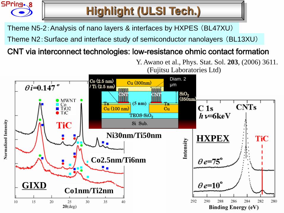
CNT via interconnect technologies: low-resistance ohmic contact formation
Ni30nm/Ti50nm
Co2.5nm/Ti6nm
Co1nm/Ti2nmGIXD
HXPEX
Y. Awano et al., Phys. Stat. Sol. 203, (2006) 3611. (Fujitsu Laboratories Ltd)
Diam. 2 μm
Theme N5-2:Analysis of nano layers & interfaces by HXPES (BL47XU)
Highlight (ULSI Tech.)
Theme N2:Surface and interface study of semiconductor nanolayers (BL13XU)

X-ray
M1
M2In-vacuum undulatorXY slit (0.2 x 0.2 mm)
Si 111 Monochromator
Sample scan
L1
L2
f53 m
Experimental setup of X-ray microbeam system at BL37XU, SPring-8
Y. Terada (JASRI) et al., AIP Conf. Proc. 705, 376 (2004)
Kirkpatrick-Baez optics with aspherical (plane parabola) mirrors,L1: 100 mm, L2: 100 mm, f: 50 mm,Glancing angle: 0.9 mrad. (Pt coated SiO2),Fabricated at Cannon Co. Japan.
Theme N7: Fluorescence X-ray trace element analysis (BL37XU)
Development K-B Mirror Optics in High-Energy X-ray Region (37keV)

XMLD around NiO L2-edge
Horizontal polarization Vertical polarization
Fov
50 μm
Ni L2-edge869.4 eV
870.6 eV
TN=520 K
F. Guo (JASRI) et al., J. Phys. C. 17, S1363 (2005).Theme N3-2: Nanoanalysis by PEEM (BL17SU)

Theme N3-1: PES and soft XMCD of novel functional nano-materials (BL25SU)
-0.01
0
0.01
XM
CD
(a.u
.)-15 -10 -5 0 5 10 15
-0.5
0
0.5
Applied field, H (kOe)
Mn
Co
MUC-AFM
-0.01
0
0.01
XM
CD
(a.u
.)-15 -10 -5 0 5 10 15
-0.5
0
0.5
Applied field, H (kOe)
Mn
Co
MUC-AFM
Highlight (Magnetic Properties)
M. Tsunoda et al., APL 89, (2006) 172501.(Tohoku Univ.)
Mcroscopic Origin and Role of Unconpensated Antiferromagnetic Spins in Mn-Ir Based Exchange Biased Bilayers
Schematic illustration of uncompensatedAFM moments induced at the interface.
Mn and Co ESMH loops of ordered Mn-Ir/Co-Fe bilayers. The hysteresis loops were obtained in the exchange bias direction either parallel (red) or antiparallel (blue) to the incident X-ray wave vector.

S.Takeda, S. Kimura (JASRI) et al., JJAP 45, L1054 (2006)
High-Resolution X-ray Microdiffractometer
Theme N2:Surface and interface study of semiconductor nanolayers (BL13XU)

Reciprocal Space Mapping of Strain-relaxed SiGe/Si Buffer Layers
Sample A Sample B
• Domain structures in a micrometer-scale area in SiGe relaxed by 60º dislocations
• Highly homogeneous strain in SiGe relaxed by pure edge dislocations
S. Mochizuki (Nagoya Univ.) et al., Thin Solid Films 508, 128 (2006).
Highlight (ULSI Tech.)Theme N2:Surface and interface study of semiconductor nanolayers (BL13XU)
SR Gr.
Advisory Board
Support Themes of Nanotechnology Support Pj at SPring-8
Ultra-HV TEM
Nano Foundries Gr.
Mol. Synth. & Anal. Gr.
Nanotech. Researchers Network Center
Ritsumeikan U. SR Center
SPring-8
N1:Element selective magnetization measurements (BL39XU)
N2:Surf. & interface study of semicond. nano-layers (BL13XU)
N3-1:PES & soft XMCD of novel functional nano-materials N3-2:Nanoanalysis by PEEM (BL25SU, 17SU)
N4:High precision powder XRD of nano-materials (BL02B2)
N5-1:CT with X-ray focused beamN5-2:Analysis of nano layers & interfaces by HEPES (BL47XU)
N6:SX spectroscopy of nano-particles and nano layers (BL27SU)
N7:Fluorescence X-ray trace element analysis (BL37XU)
N8:Studies on local structures & electronic states using NRS (BL11XU)
N9:Structure analysis between solid/liquid interfaces (BL14B1)
N10:In situ PES for ultra-thin layer formation processes (BL23SU)
N13:In situ observation of layer-by-layer crystal growth (BL11XU)
N14:Static and dynamical structure study (BL22XU)
N12:High energy inner shell PES (BL15XU)
N11:The nano aggregate analysis by a high-precise SAX (BL15XU)JASR
IJAEA
NIM
S
Facilities
Each BL uses about 20 % beamtime for the project.

Activities of Nanotechnology Support Project
1. Additional supports(A) Support for the planning of ideal experiment plan (B) Technical support (C) Advice to analyses/evaluation of research results
These supports enable various nanotechnology researchers, who have not experienced synchrotron radiation researches, to perform the experiments effectively and efficiently.
2. Promotion of nanotechnology researches using SR
• An annual meeting on the results of research activities by SR group of the Nanotechnology Support Pj is held.
• Workshop of the each theme is held a few times a year.
• Various information for the “Nanotechnology Support Pj” is introduced through the website and publications.

In-vacuum undulatorXY slit (0.2 x 0.2 mm)
Si 111 Monochromator
Sample scan
L1
L2
f53 m
Y. Terada (JASRI) et al., AIP Conf. Proc. 705, 376 (2004)
Theme N7: Fluorescence X-ray trace element analysis (BL37XU)
Development K-B Mirror Optics in High-Energy X-ray Region (37keV)
A. Hokura etal., Chemistry Lett. 35, 1246 (2006)(Tokyo Univ. of Sci.)

Plans for Nano Science and Technology at SSRF
SR applications to nano (material) will surely be an important part at SSRF from now on. In fact, all of the first phase can be relevant to the nano-field.
In particular, we have got a 30nm soft x-ray beam (EPU,250-2000eV) by zone plate, and a 2 microns hard x-ray beam(in vacuun undulator,3.5-22.5keV) by KB mirror.
A mutipolar wiggler beam line for XAFS has also great potential.
As next step, we have an upgrading program supported by CAS to construct a X-ray interference lithiography (XIL) as a branch line of current soft x-ray beamline.
XIL by SR is unique in fabrication of high throughput, large-area, tens-of-nano-sized, periodic template which can be applied to many fields.
A 100nm hard x-ray beam will also come soon by zone plate focusing.

Nano Probes at NSRRC, Taiwan
Lateral resolution [nm]
Che
mic
al in
form
atio
n 30 nm
5μm
90 nm 70 nm
(spatial resolution)
8μm
1
1. Lung cancer cell by phase contrast image2. IC tungsten plugs with key-hole defects
1
2
APL 88, 241115 (2006); 90, 181118 (2007)