application note w-cdma test -...
TRANSCRIPT

Application Note
W-CDMA TestMG3700A Vector Signal Generator

1
Slide 1MG3700A-E-F-6
Application Note- W-CDMA Test -
Anritsu
February 2007(4.00)
Slide 2MG3700A-E-F-6
Contents
• Physical Channel Basics 3• BS Test 16• UE Test 65• Repeater Test 118• Additional Information 142

2
Slide 3MG3700A-E-F-6
UTRA/FDD Frequency Bands
Japan875 – 885830 – 8402 × 10800VI
USA, Asia869 – 894824 – 8492 × 25850V
EU, Asia925 – 960880 – 9152 × 35900VIII
Japan1845 – 18801750 – 17852 × 351700IX
EU, Asia, Brazil
1805 – 18801710 – 17852 × 751800III
3G band in USA
2110 – 21551710 – 17552 × 451700/2100IV
PCS band in USA
1930 – 19901850 – 19102 × 601900II
UMTS core band
2110 – 21701920 – 19802 × 602100I
New2620 – 26902500 – 25702 × 702600VII
Downlink[MHz]
Uplink[MHz]
Bandwidth[MHz]
BandTitle
OperatingBand
Slide 4MG3700A-E-F-6
HSPA Standardization in 3GPP
• HSDPA (High-speed Downlink Packet Access) was standardized in 3GPP Release 5.
» The downlink peak data rate will increase to 3.6 Mbps, 7.2 Mbps and potentially beyond 10 Mbps.
» HS-DSCH– HARQ for downlink– Fast BTS downlink scheduling– Shorter downlink TTI– Higher order and adaptive modulation
• HSUPA (High-speed Uplink Packet Access) was standardized in 3GPP Release 6.
» The uplink peak data rate will increase to 1 to 2 Mbps and 3 to 4 Mbps.
» E-DCH– HARQ for uplink– Fast BTS uplink scheduling– Shorter uplink TTI

3
Slide 5MG3700A-E-F-6
HSDPA UE Capabilities (Categories)
• 3GPP TS 25.306 specifies UE capabilities for HS-DSCH categories.
– Category 1 to 10 support 16QAM and QPSK. Category 11 and 12 support QPSK only.
1.8363015120.93630251114.4279521151010.22025111597.21441111087.21441111073.672981563.672981551.872982541.872982531.272983521.27298351
Achievable Maximum Data
Rate[Mbps]
Maximum Number of Transport
Channel Bits per HS-DSCH
TTI
Minimum Inter-TTI Interval
Maximum Number of HS-PDSCH Codes
Category
Slide 6MG3700A-E-F-6
HSUPA UE Capabilities (Categories)
• 3GPP TS 25.306 specifies UE capabilities for E-DCH categories.
– All categories support 10 ms TTI.
5.7210 ms and 2 ms
2 × SF2 + 2 ×SF4
6-210 ms2 × SF25
2.8210 ms and 2 ms
2 × SF24-1.410 ms2 × SF43
1.31.410 ms and 2 ms
2 × SF42-0.710 ms1 × SF41
Maximum Data Rate with 2 ms
TTI[Mbps]
Maximum Data Rate with 10
ms TTI[Mbps]
Support for 10 and 2 ms TTI
Maximum Number of E-
DPDCH Codes,
Minimum SF
Category

4
Slide 7MG3700A-E-F-6
Mapping of Transport Channels onto Physical Channels
Transport Channels– DCH
– E-DCH
– RACH
– BCH– FACH– PCH
– HS-DSCH
Physical Channels– DPDCH Dedicated Physical Data Channel– DPCCH Dedicated Physical Control Channel– F-DPCH Fractional Dedicated Physical Channel– E-DPDCH E-DCH Dedicated Physical Data Channel– E-DPCCH E-DCH Dedicated Physical Control Channel– E-AGCH E-DCH Absolute Grant Channel– E-RGCH E-DCH Relative Grant Channel– E-HICH E-DCH Hybrid ARQ Indicator Channel– PRACH Physical Random Access Channel– CPICH Common Pilot Channel– P-CCPCH Primary Common Control Physical Channel– S-CCPCH Secondary Common Control Physical Channel– SCH Synchronization Channel– AICH Acquisition Indicator Channel– PICH Paging Indicator Channel– MICH MBMS Notification Indicator Channel– HS-PDSCH High Speed Physical Downlink Shared Channel– HS-SCCH HS-DSCH-related Shared Control Channel– HS-DPCCH Dedicated Physical Control Channel (uplink) for HS-DSCH
HSUPA
HSDPA
Slide 8MG3700A-E-F-6
Basic Physical Channels
SCHCPICH
P-CCPCHS-CCPCH
AICHPICH
DPCH
PRACH
DPCCHDPDCH

5
Slide 9MG3700A-E-F-6
HSDPA Physical Channels
HS-SCCHHS-PDSCH
HS-DPCCH
(DPCCH)(DPDCH)
Slide 10MG3700A-E-F-6
HSUPA Physical Channels
E-HICH/E-RGCHE-AGCH
E-DPCCHE-DPDCH
(DPCCH)(DPDCH)

6
Slide 11MG3700A-E-F-6
Downlink Physical Channels
• Common Channels» SCH is an un-encoded channel that is broadcast over the entire
cell. SCH allows UEs to acquire the cell. SCH exists only at the physical layer.
» CPICH is a channel that exists only at the physical layer. Its function is to assist the UE in channel estimation for dedicatedor common physical channels. CPICH is scrambled with the cell-specific primary scrambling code.
» P-CCPCH and S-CCPCH are common physical channels intended for carrying system and cell information and messages for UEs when a dedicated channel is not in place for communication.
» PICH is a channel that exists only at the physical layer. It is usedto notify UEs of outstanding paging messages on the Paging Channel (PCH). It saves UE battery power.
Slide 12MG3700A-E-F-6
Downlink Physical Channels
• Common Channels» AICH is a channel that exists only at the physical layer. AICH
sends status indicators on the downlink, reflecting the state (busy or idle) of the Random Access Channel (RACH). This allows UEs to verify the state of the access channel before transmission, which helps to minimize collisions.
» HS-PDSCH is a shared channel across all users requesting HSDPA specific high-speed packet data services. Each cell may support one or more HS-PDSCHs. Sharing of the HS-PDSCH is based on Time-Division Multiplexing (TDM) across multiple users.
» HS-SCCH is a control channel associated with the HS-PDSCH. HS-SCCH conveys the HS-PDSCH allocation information including the user identity, the number of spreading factors, and modulation scheme.

7
Slide 13MG3700A-E-F-6
Downlink Physical Channels
• Common Channels» E-AGCH is used for transmitting the absolute value of the BTS
scheduler decision informing the UE about the relative transmission power it may use for data channel transmission (E-DPDCH), effectively telling the UE the maximum transmission data rate it may use.
Slide 14MG3700A-E-F-6
Downlink Physical Channels
• Dedicated Channels» DPDCH and DPCCH are the dedicated physical channels
targeted to transport information between the network and the UE using a dedicated link on the physical channel. They are both time multiplexed and carried on the DPCH.
» E-RGCH is used for transmitting single set-up/down scheduling commands that affect the relative transmission power the UE may use for data channel transmission (E-DPDCH), effectively adjusting the uplink data rate up/down.
» E-HICH is used for transmitting positive and negative acknowledgements for uplink packet transmission.
» F-DPCH is basically a stripped-down version of DPCH that handles the power control. Only the TPC field is kept when comparing F-DPCH with DPCH. F-DPCH is used in cases that DCH causes too much overhead and consumes too much code space when accepting a large number of users using a low data rate service, like VoIP.

8
Slide 15MG3700A-E-F-6
Uplink Physical Channels
• Common Channels» PRACH is shared by UEs. It is used for initial access of the
system.
• Dedicated Channels» DPDCH and DPCCH are separated due to potential audio
interference that may be caused in the UE, such as a mobile phone.
» HS-DPCCH carries the feedback signalling related to downlink HS-DSCH (incoming packets). The HS-DSCH-related feedback signalling consists of Hybrid-ARQ Acknowledgement (HARQ-ACK) and Channel-Quality Indication (CQI).
» E-DPDCH is used for transmitting E-DCH transport channel processing from the UE to the BS.
» E-DPCCH is used for transmitting control information aboutE-DPDCH transmission from the UE to the BS.
Slide 16MG3700A-E-F-6
BS Test
Performance of signaling detection for E-DPCCH in multipath fading conditions8.13
MA1612A3 GHzCombiner
FadingSimulator
MG3700ADemodulation of E-DPDCH in multipath fading conditions8.12
CodeDomainAnalyzer
MG3700AOutput power dynamicsPower control stepsPower control dynamic range
6.46.4.26.4.3
*: MG3700A for wanted signal generator generates two signals with interference signal, CW or AWGN.
*Performance of signaling detection for HS-DPCCHACK false alarm in static propagation conditionsACK mis-detection in static propagation conditions
8.118.11.18.11.3
Verification of the internal BLER calculation8.6Demodulation of DCH in birth/death propagation conditions8.5
Demodulation of DCH in moving propagation conditions8.4
MA1612A3 GHzCombiner
FadingSimulator
MG3700A
Demodulation of DCH in multipath fading conditions8.3*Demodulation in static propagation conditions8.2
Verification of the internal BER calculation7.8
MA1612A3 GHzCombiner*Intermodulation characteristics7.6
MG3692B20 GHz
orMG3642A2.08 GHz
*Blocking characteristics7.5*Adjacent Channel Selectivity (ACS)7.4
*Dynamic range7.3
MG3700A
Reference sensitivity level7.2
SpectrumAnalyzerCirculator
MG3700ATransmit intermodulation6.6
OthersAWGNGenerator
CWGenerator
InterferenceSignalGenerator
WantedSignalGeneratorwith BERT
Test
TS 25.141 (Release 7)TransmitterReceiverPerformance requirement
3GPP678

9
Slide 17MG3700A-E-F-6
CW Generator(MG3692B)
Controller
Combiner(MA1612A)
Terminator(MP752A)
Receiver Test Connection Example
– Start trigger• Front panel [Start/Frame Trigger] Input
– 40 ms × n clocke.g. SFN reset timing of Downlink BCH (4096 frame × 10 ms)
– Reference clockUse only one.• Rear panel [Baseband Ref Clock] Input
– 3.84 MHz, 2 × 3.84 MHz (7.68 MHz), 4 × 3.84 MHz (15.36 MHz)• Rear panel [10MHz/5MHz Ref] Input
– Controller• Makes receivable state for UL RMC by FTM (Factory Test Mode) control• Reports internal BER/BLER calculation for received DTCH
Wanted Signal Generator(+ Interference Signal Generator)(+ CW Generator)(+ AWGN Generator)BER TesterMG3700A
Reference clock
Clock
Received DTCH data
Start trigger
Slide 18MG3700A-E-F-6
Timing Synchronization Setup Example
• Start trigger delay» Set the timing at which the BS can receive UL RMC.
Radio frameDL DPCH
Trigger
FN=4N FN=4N+1 FN=4N+2 FN=4N+3
Delay: 0 chip
SFN reset(SFN=2047)
DCCH
DTCH DTCHUL DCH
1 frame
Delay: 1,024 chips (T0)
10 ms38,400 chips 40 ms
UL DPDCH/DPCCH DPCH DPCH DPCH DPCH
DCCH
DTCHDL DCH DTCH

10
Slide 19MG3700A-E-F-6
Timing Synchronization Setup Example
• Setting external start trigger» Captures/ Synchronizes
trigger once only
• Reference clock» [Baseband Ref Clock] Input
usage case– Source: [External]– Baseband Reference Clock:
• [1],[1/2],[1/4],[1/8],[1/16] ×» [10MHz/5MHz Ref] Input usage
case– Source: [Internal]
• Trigger recapture/ synchronization
Slide 20MG3700A-E-F-6
Wanted Signal SetupHSPA or Limited W-CDMA IQproducer
• Created sample rate– 3 × Oversampling
DTCH DCCH
License option MX370101A
Non-license

11
Slide 21MG3700A-E-F-6
• UL RMC 12.2 kbps
• UL RMC 64 kbps
• UL RMC 144 kbps
• UL RMC 384 kbps
Wanted Signal SetupHSPA or Limited W-CDMA IQproducer
Slide 22MG3700A-E-F-6
Scrambling Code SynchronizationSetup Example
• Scrambling code» BS identifies UE by scrambling code allocated to each UE.» 38,400 chips (10 ms) segments
– Created from 25-bit long Gold sequences» Applies HPSK modulation to scrambling (spreading)
• Set the initial condition xn(23) ∼ xn(0) receivable by BS.– 0 ∼ 16,777,215

12
Slide 23MG3700A-E-F-6
Wanted Signal Setup Example
Test– Receiver
• UL RMC 12.2 kbps– Scrambling Code 0H
» For mixing interference signal
– 3 × Oversampling• Frequency offset
≤ 34.944 MHz
– 4 × Oversampling• Frequency offset
≤ 47.232 MHz
Both signal patterns are the same.
Slide 24MG3700A-E-F-6
Wanted Signal Setup Example
Test– Dynamic range– Performance requirements
• UL RMC 12.2 kbps• UL RMC 64 kbps• UL RMC 144 kbps• UL RMC 384 kbps
– Scrambling Code 0H» For mixing AWGN
– 3 × Oversampling

13
Slide 25MG3700A-E-F-6
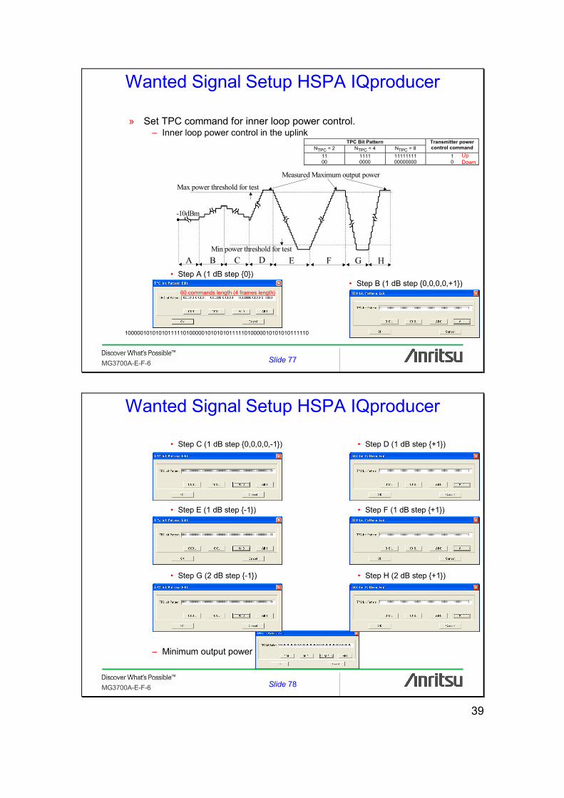
Wanted Signal Setup HSPA IQproducer
Test– Power control steps– Power control dynamic range
• UL RMC 12.2 kbps
DTCH DCCH
Slide 26MG3700A-E-F-6
Wanted Signal Setup HSPA IQproducer
» Set TPC command for inner loop power control.– Power control steps
• Transmitter power control step tolerance
• Transmitter aggregated power control step range
– Power control dynamic range
TPC Bit Pattern NTPC = 2
Transmitter power control command
11 00
1 0
60 commands length (4 frames length)
10 consecutive equal commands
Test Model 2 DPCH
UpDown
Pmax -3 dB ≤-28 dB ≥-3 dB

14
Slide 27MG3700A-E-F-6
Wanted Signal Setup HSPA IQproducer
Test– Verification of the internal BER calculation
– Verification of the internal BLER calculation
• UL RMC 12.2 kbps
Informationdata
BERinsertion
CRCattachment
TrBk concatenation/Code block segment
Channelcoding
Radio frameequalization
1st interleaving Radio framesegmentation
Rate matching TrCHmultiplexing
PhysicalChannelsegmentation
2nd interleavingPhysicalChannelmapping
PhCHPN9 1 %
Informationdata
CRCattachment
CRC errorinsertion
TrBk concatenation/Code block segment
Channelcoding
Radio frameequalization
1st interleaving Radio framesegmentation
Rate matching TrCHmultiplexing
PhysicalChannelsegmentation
2nd interleavingPhysicalChannelmapping
PhCHPN9 1 %
%
Slide 28MG3700A-E-F-6
Wanted Signal Setup HSPA IQproducer
Test– ACK mis-detection in static propagation conditions
• RMC HS-DPCCH• Each power ratio normalized automatically
from total powerFor example Normalize
– DPCCH: -4.56 dB >> -5.86 dB– DPDCH: -1.87 dB >> -3.17 dB– HS-DPCCH (ACK): -4.56 dB >> -5.86 dB– HS-DPCCH (CQI): -4.56 dB >> -5.86 dB
• Resolution 1 symbol (bit)
• Custom-designed pattern file for HS-DPCCHup to 2,048 radio frames
• Supports separate editing of power ofHARQ-ACK (ACK), (NACK) and CQI
Q I Q
DPCCH DPDCH HS-DPCCHCode
Total power
ACK CQI NACK CQI
Power
t
Maximum power
HS-DPCCH
Power

15
Slide 29MG3700A-E-F-6
Wanted Signal Setup HSPA IQproducer
Test– Demodulation of E-DPDCH in multipath fading conditions– Performance of signaling detection for E-DPCCH in multipath fading
conditions• E-DPDCH FRC
Fixed Ref Channel
TTI [ms]
NINF SF1 SF2 SF3 SF4 NBIN Coding rate
Max inf bit rate [kbps]
FRC1 2 2706 4 4 0 0 3840 0.705 1353.0 FRC2 2 5412 2 2 0 0 7680 0.705 2706.0 FRC3 2 8100 2 2 4 4 11520 0.703 4050.0 FRC4 10 5076 4 0 0 0 9600 0.529 507.6 FRC5 10 9780 4 4 0 0 19200 0.509 978.0 FRC6 10 19278 2 2 0 0 38400 0.502 1927.8 FRC7 10 690 16 0 0 0 2400 0.288 69.0
E-DPDCH/DPCCH power ratio: 12.04 dBE-DPDCHs power = -20 + 12.04 + 10 log (2 codes) = -4.95
Total E-DPDCHs power* 3GPP standard shows E-DPDCH/DPCCH power ratio for single E-DPDCH. -4.95
-20
-13.98
Slide 30MG3700A-E-F-6
Wanted Signal Setup HSPA IQproducer
– The following information is transmitted by E-DPCCH.• Retransmission sequence number (RSN): xrsn (2 bits)
– RSN informs the HARQ sequence number of the transport block currently being sent on E-DPDCHs. The initial transmission of a transport block is sent with RSN = 0, the first with RSN = 1, the second with RSN = 2, and all subsequent transmissions with RSN = 3.
• E-TFCI: xtfci (7 bits)– E-TFCI, the E-DCH transport format combination indicator, indicates the transport format
being transmitted simultaneously on E-DPDCHs, and tells the BS the transport block size coded on the E-DPDCH. From this information, the BS can derive how many E-DPDCHsare transmitted in parallel and what SF is used.
• "Happy" bit: xh (1 bit)– The “Happy” bit indicates whether the UE is satisfied with the current data rate (or relative
power allowed to be used for E-DPDCHs) or whether it could use higher power allocation.Nsys / Ne,data,j <1/2 1/2 ≤ Nsys / Ne,data,j RSN Value E-DCH RV Index E-DCH RV Index
0 0 0 1 2 3 2 0 2 3 [ TTIN/NARQ mod 2 ] x 2 TTIN/NARQ mod 4
"Happy" bit xh,1 Happy 1
Not happy 0
Information Bit Payload NINF = 2706
CRC Addition
3 x (NINF+24) = 8190
Code Block Segmentation 2706+24 = 2730
Turbo Encoding (R=1/3)
RV Selection 3840
Physical Channel Segmentation 1920
24 NINF = 2706
12
1920 2 codes E-DPDCHs
TTI period

16
Slide 31MG3700A-E-F-6
Transport Block SizeE-TFCI TB Size
(bits) E-TFCI TB Size
(bits) E-TFCI TB Size
(bits)
0 18 43 2724 86 7252 1 186 44 2742 87 7288 2 204 45 3042 88 7428 3 354 46 3060 89 7464 4 372 47 3078 90 7764 5 522 48 3298 91 7800 6 540 49 3316 92 7908 7 674 50 3334 93 7944 8 690 51 3378 94 8100 9 708 52 3396 95 8136
10 726 53 3414 96 8436 11 858 54 3732 97 8472 12 876 55 3750 98 8564 13 1026 56 3972 99 8600 14 1044 57 3990 100 8772 15 1062 58 4068 101 8808 16 1194 59 4086 102 9108 17 1212 60 4404 103 9144 18 1330 61 4422 104 9220 19 1348 62 4628 105 9256 20 1362 63 4646 106 9444 21 1380 64 4740 107 9480 22 1398 65 4758 108 9780 23 1530 66 5076 109 9816 24 1548 67 5094 110 9876 25 1698 68 5284 111 9912 26 1716 69 5302 112 10116 27 1734 70 5412 113 10152 28 1866 71 5430 114 10452 29 1884 72 5748 115 10488 30 1986 73 5766 116 10532 31 2004 74 5940 117 10568 32 2022 75 5958 118 10788 33 2034 76 6084 119 10824 34 2052 77 6102 120 11124 35 2070 78 6420 121 11178 36 2370 79 6438 122 11188 37 2388 80 6596 123 11242 38 2406 81 6614 124 11460 39 2642 82 6756 125 11478 40 2660 83 6774 41 2678 84 7092 42 2706 85 7110
3GPP TS 25.321 Annex B.2 2 ms TTI
E-TFCI TB Size (bits)
E-TFCI TB Size (bits)
E-TFCI TB Size (bits)
0 18 41 5076 82 11850 1 186 42 5094 83 12132 2 204 43 5412 84 12186 3 354 44 5430 85 12468 4 372 45 5748 86 12522 5 522 46 5766 87 12804 6 540 47 6084 88 12858 7 690 48 6102 89 13140 8 708 49 6420 90 13194 9 858 50 6438 91 13476
10 876 51 6756 92 13530 11 1026 52 6774 93 13812 12 1044 53 7092 94 13866 13 1194 54 7110 95 14148 14 1212 55 7428 96 14202 15 1362 56 7464 97 14484 16 1380 57 7764 98 14556 17 1530 58 7800 99 14820 18 1548 59 8100 100 14892 19 1698 60 8136 101 15156 20 1716 61 8436 102 15228 21 1866 62 8472 103 15492 22 1884 63 8772 104 15564 23 2034 64 8808 105 15828 24 2052 65 9108 106 15900 25 2370 66 9144 107 16164 26 2388 67 9444 108 16236 27 2706 68 9480 109 16500 28 2724 69 9780 110 16572 29 3042 70 9816 111 17172 30 3060 71 10116 112 17244 31 3378 72 10152 113 17844 32 3396 73 10452 114 17916 33 3732 74 10488 115 18516 34 3750 75 10788 116 18606 35 4068 76 10824 117 19188 36 4086 77 11124 118 19278 37 4404 78 11178 119 19860 38 4422 79 11460 120 19950 39 4740 80 11514 40 4758 81 11796
3GPP TS 25.321 Annex B.4 10 ms TTI
Slide 32MG3700A-E-F-6
Wanted Signal Setup HSPA IQproducer
• FRC1 » 1 Radio frame length pattern
» Arbitrary TTI length pattern
Save as CSV

17
Slide 33MG3700A-E-F-6
Wanted Signal Setup HSPA IQproducer
• FRC2 » 1 Radio frame length pattern
» Arbitrary TTI length pattern
Save as CSV
Slide 34MG3700A-E-F-6
Wanted Signal Setup HSPA IQproducer
• FRC3 » 1 Radio frame length pattern
» Arbitrary TTI length pattern
Save as CSV

18
Slide 35MG3700A-E-F-6
Wanted Signal Setup HSPA IQproducer
• FRC4 » 1 Radio frame length pattern
» Arbitrary TTI length pattern
Save as CSV
Slide 36MG3700A-E-F-6
Wanted Signal Setup HSPA IQproducer
• FRC5 » 1 Radio frame length pattern
» Arbitrary TTI length pattern
Save as CSV

19
Slide 37MG3700A-E-F-6
Wanted Signal Setup HSPA IQproducer
• FRC6 » 1 Radio frame length pattern
» Arbitrary TTI length pattern
Save as CSV
Slide 38MG3700A-E-F-6
Wanted Signal Setup HSPA IQproducer
• FRC7 » 1 Radio frame length pattern
» Arbitrary TTI length pattern
Save as CSV

20
Slide 39MG3700A-E-F-6
Wanted Signal + Interference SignalSetup Example
Test– ACS– Blocking characteristics– Intermodulation characteristics
• UL RMC 12.2 kbps+
• UL Interferer» Set frequency offset.
– -34.944 ∼ +34.944 MHz• 3 × Oversampling
– -47.232 ∼ +47.232 MHz• 4 × Oversampling
StaticVariableVariableConstant
CoupledVariableStaticB
CoupledStaticVariableA
RF levelB levelA levelA/B Set
UL RMC
Interferer
Carrier leakage
ACS: 5 MHz offsetBlocking: ≥ 10 MHz offsetIntermodulation:20 MHz offset
Slide 40MG3700A-E-F-6
Wanted Signal + GMSK Interference SignalSetup Example
Test– Blocking characteristics– Intermodulation characteristics
Requires about 1 day to complete, depending on the PC specificationsAvailable frequency offset between wanted signal and GMSK interference signal
UL RMC 12.2 kbps: 4 × OversamplingUL RMC 12.2 kbps: 3 × Oversampling
Resampling
License option MX370104A

21
Slide 41MG3700A-E-F-6
Wanted Signal + GMSK Interference SignalSetup Example
• UL RMC 12.2 kbps+
• GMSK Interferer» Set frequency offset.
– -39.68 ∼ +39.68 MHz• Based on 3 × Oversampling
– -60.48 ∼ +60.48 MHz• Based on 4 × Oversampling
StaticVariableVariableConstant
CoupledVariableStaticB
CoupledStaticVariableA
RF levelB levelA levelA/B Set
Interferer
Carrier leakage
UL RMC-48 dB
Blocking: ≥ 2.7 MHz offsetIntermodulation:5.9 MHz offset
S/N:-70.1 dB/3.84 MHz (-91.2 dB/30 kHz) * 2.7 MHz offset-73.1 dB/3.84 MHz (-94.2 dB/30 kHz) * 5.9 MHz offsetSSB phase noise:-136 dBc/Hz typ. * 2.7 MHz offset-139 dBc/Hz typ. * 5.9 MHz offset
-58 dB
-68 dB
Slide 42MG3700A-E-F-6
Wanted Signal + AWGN Setup Example
Test– Dynamic range– Demodulation in static
propagation conditions• UL RMC 12.2 kbps• UL RMC 64 kbps• UL RMC 144 kbps• UL RMC 384 kbps
+• AWGN
» Ioc [dBm/3.84MHz]» Wanted signal level/AWGN [dB]
= 10log10(Rb/3.84×106) + Eb/No∼∼∼∼∼∼∼∼∼∼∼∼∼∼∼∼∼
– Rb bps ↓↓12.2 k: -24.9864 k: -17.78
144 k: -14.26384 k: -10
– Eb/No is specified in test requirements.
StaticVariableVariableConstant
CoupledVariableStaticB
CoupledStaticVariableA
RF levelB levelA levelA/B Set

22
Slide 43MG3700A-E-F-6
Wanted Signal Parameters
• UL RMC
Parameter DCH for DTCH / DCH for DCCH Unit Information bit rate 12,2/2,4 64/2,4 144/2,4 384/2,4 2048/2,4 kbps Physical channel 60/15 240/15 480/15 960/15 960/15 kbps Spreading factor 64 16 8 4 4 Repetition rate 22/22 19/19 8/9 -18/-17 -7/-7 % Interleaving 20 40 40 40 80 ms
DPDCH
Number of DPDCHs 1 1 1 1 6 Dedicated pilot 6 bit/slot Power control 2 bit/slot TFCI 2 bit/slot FBI 0 / 2 bit/slot
DPCCH
Spreading factor 256 Power ratio of DPCCH/DPDCH
-2,69 -5,46 -9,54 -9,54 -9,54 dB
Amplitude ratio of DPCCH/DPDCH
0,7333 0,5333 0,3333 0,3333 03333
Note: Combination of TFCI bit of 0 bit/slot and FBI bit of 2 bit /slot is applied in test of Site Selection Diversity Transmission specified in 8.10.
Slide 44MG3700A-E-F-6
DPDCH/DPCCH Structure of UL RMC
Pilot Npilot bits
TPC NTPC bits
DataNdata bits
Slot #0 Slot #1 Slot #i Slot #14
Tslot = 2560 chips, 10 bits
1 radio frame: Tf = 10 ms
DPDCH
DPCCHFBI
NFBI bitsTFCI
NTFCI bits
Tslot = 2560 chips, Ndata = 10*2k bits (k=0..6)
Slot Format #i Channel Bit Rate (kbps)
Channel Symbol Rate (ksps)
SF Bits/ Frame
Bits/ Slot
Ndata
0 15 15 256 150 10 10 1 30 30 128 300 20 20 2 60 60 64 600 40 40 3 120 120 32 1200 80 80 4 240 240 16 2400 160 160 5 480 480 8 4800 320 320 6 960 960 4 9600 640 640
Slot Format #i
Channel Bit Rate (kbps)
Channel Symbol Rate (ksps)
SF Bits/ Frame
Bits/Slot
Npilot NTPC NTFCI NFBI Transmitted slots per
radio frame0 15 15 256 150 10 6 2 2 0 15
0A 15 15 256 150 10 5 2 3 0 10-14 0B 15 15 256 150 10 4 2 4 0 8-9 1 15 15 256 150 10 8 2 0 0 8-15 2 15 15 256 150 10 5 2 2 1 15
2A 15 15 256 150 10 4 2 3 1 10-14 2B 15 15 256 150 10 3 2 4 1 8-9 3 15 15 256 150 10 7 2 0 1 8-15
PN9
I
Q
Alternate 00/11
Npilot = 6 Bit # 0 1 2 3 4 5
Slot #0 1 2 3 4 5 6 7 8 9 10 11 12 13 14
1 1 1 1 1 1 1 1 1 1 1 1 1 1 1
1 0 0 0 1 1 1 1 0 1 0 1 1 0 0
1 0 1 0 0 1 1 0 1 1 1 0 0 0 0
1 1 1 1 1 1 1 1 1 1 1 1 1 1 1
1 1 0 0 0 1 0 0 1 1 0 1 0 1 1
001010000111011
12.2 kbps
64 kbps144 kbps384 kbps

23
Slide 45MG3700A-E-F-6
Wanted Signal Parameters
• UL RMC 12.2 kbps
Parameter Level Unit Information bit rate 12,2 kbps DPCH 60 kbps Power control Off TFCI On Repetition 22 %
Slide 46MG3700A-E-F-6
Wanted Signal Parameters
• UL RMC 64 kbps
Parameter Level Unit Information bit rate 64 kbps DPCH 240 kbps Power control Off TFCI On Repetition 19 %

24
Slide 47MG3700A-E-F-6
Wanted Signal Parameters
• UL RMC 144 kbps
Parameter Level Unit Information bit rate 144 kbps DPCH 480 kbps Power control Off TFCI On Repetition 8 %
Slide 48MG3700A-E-F-6
Wanted Signal Parameters
• UL RMC 384 kbps
Parameter Level Unit Information bit rate 384 kbps DPCH 960 kbps Power control Off TFCI On Puncturing 18 %

25
Slide 49MG3700A-E-F-6
Wanted Signal Parameters
• RMC HS-DPCCH
Subframe #0 Subframe # i Subframe #4
HARQ-ACK CQI
One radio frame T f = 10 ms
One HS-DPCCH subframe (2 ms)
2 × T slot = 5120 chipsT slot = 2560 chips
CQI mapping table for UE categories 1 to 6.
CQI valueTransport
Block Size
Number of
HS-PDSCHModulation
Reference power
adjustment ∆
NIR XRV
0 N/A Out of range
1 137 1 QPSK 0
2 173 1 QPSK 0
3 233 1 QPSK 0
4 317 1 QPSK 0
5 377 1 QPSK 0
6 461 1 QPSK 0
7 650 2 QPSK 0
8 792 2 QPSK 0
9 931 2 QPSK 0
10 1262 3 QPSK 0
11 1483 3 QPSK 0
12 1742 3 QPSK 0
13 2279 4 QPSK 0
14 2583 4 QPSK 0
15 3319 5 QPSK 0
16 3565 5 16-QAM 0
17 4189 5 16-QAM 0
18 4664 5 16-QAM 0
19 5287 5 16-QAM 0
20 5887 5 16-QAM 0
21 6554 5 16-QAM 0
22 7168 5 16-QAM 0
23 7168 5 16-QAM -1
24 7168 5 16-QAM -2
25 7168 5 16-QAM -3
26 7168 5 16-QAM -4
27 7168 5 16-QAM -5
28 7168 5 16-QAM -6
29 7168 5 16-QAM -7
30 7168 5 16-QAM -8
9600 0
Parameter Unit Information bit rate 12.2 kbps Physical channel 60 kbps DTCH Repetition rate 22 % Information bit rate 2.4 kbps Physical channel 15 kbps DCCH Repetition rate 22 %
Spreading factor 64 Interleaving 20 ms
DPDCH
Number of DPDCHs 1 Dedicated pilot 6 Bits/slot Power control 2 Bits/slot TFCI 2 Bits/slot
DPCCH
Spreading factor 256 Power ratio of DPCCH/DPDCH -2.69 dB Amplitude ratio of DPCCH/DPDCH 0.7333 Closed loop power control OFF Repetition factor of ACK/NACK 1 HS-DPCCH power offset to DPCCH 0 dB HS-DPCCH timing offset to DPCCH 0 symbol
Slot Format #i Channel Bit
Rate (kbps)
Channel Symbol
Rate (ksps)
SF Bits/
Subframe
Bits/
Slot
Transmitted
slots per
Subframe
0 15 15 256 30 10 3
Same asUL RMC 12.2 kbps
Slide 50MG3700A-E-F-6
Wanted Signal Parameters
• E-DPDCH FRC(UL HSUPA)
Data, Ndata bits
Slot #1 Slot #14Slot #2 Slot #i Slot #0
Tslot = 2560 chips, Ndata = 10*2k bits (k=0…7)
Tslot = 2560 chips
1 subframe = 2 ms
1 radio frame, Tf = 10 ms
E-DPDCH E-DPDCH
E-DPCCH 10 bits
Slot Format #i Channel Bit Rate (kbps)
SF Bits/ Frame
Bits/ Subframe
Bits/Slot Ndata
0 15 256 150 30 10 1 30 128 300 60 20 2 60 64 600 120 40 3 120 32 1200 240 80 4 240 16 2400 480 160 5 480 8 4800 960 320 6 960 4 9600 1920 640 7 1920 2 19200 3840 1280
Slot Format #i Channel Bit Rate (kbps)
SF Bits/ Frame
Bits/ Subframe
Bits/Slot Ndata
0 15 256 150 30 10

26
Slide 51MG3700A-E-F-6
Wanted Signal Parameters
• E-DPDCH FRC1
Information Bit Payload NINF = 2706
CRC Addition
3 x (NINF+24) = 8190
Code Block Segmentation 2706+24 = 2730
Turbo Encoding (R=1/3)
RV Selection 3840
Physical Channel Segmentation 1920
24NINF = 2706
12
1920
Parameter Unit Value Maximum. Inf. Bit Rate kbps 1353.0 TTI ms 2 Number of HARQ Processes Processes 8 Information Bit Payload (NINF) Bits 2706 Binary Channel Bits per TTI (NBIN) (3840 / SF x TTI sum for all channels)
Bits 3840
Coding Rate (NINF/ NBIN) 0.705 Physical Channel Codes SF for each
physical channel {4,4}
E-DPDCH testing: E-DPDCH/DPCCH power ratio E-DPCCH/DPCCH power ratio
dB dB dB dB
Diversity: 8.94 Non-diversity: 12.04 Diversity: 2.05 Non-diversity: 6.02 E-DPDCH /DPCCH power ratio is calculated for a single E-DPDCH.
E-DPCCH missed detection testing: E-DPDCH/DPCCH power ratio E-DPCCH/DPCCH power ratio
dB dB dB dB
Diversity: 8.94 Non-diversity: 12.04 Diversity: -1.94 Non-diversity: 0.00
Slide 52MG3700A-E-F-6
Wanted Signal Parameters
• E-DPDCH FRC2Parameter Unit Value
Maximum. Inf. Bit Rate kbps 2706.0 TTI ms 2 Number of HARQ Processes Processes 8 Information Bit Payload (NINF) Bits 5412 Binary Channel Bits per TTI (NBIN) (3840 / SF x TTI sum for all channels)
Bits 7680
Coding Rate (NINF/ NBIN) 0.705 Physical Channel Codes SF for each
physical channel {2,2}
E-DPDCH testing: E-DPDCH/DPCCH power ratio E-DPCCH/DPCCH power ratio
dB dB dB dB
Diversity: 9.92 Non-diversity: 13.00 Diversity: 4.08 Non-diversity: 6.02 E-DPDCH /DPCCH power ratio is calculated for a single E-DPDCH.
Information Bit Payload NINF = 5412
CRC Addition
3 x (NINF+24)/2 = 8154
Code Block Segmentation (5412+24)/2 = 2718
Turbo Encoding (R=1/3)
RV Selection 7680
Physical Channel Segmentation 3840
24NINF = 5412
12
(5412+24)/2 = 2718
3840
3 x (NINF+24)/2 = 8154 12

27
Slide 53MG3700A-E-F-6
Wanted Signal Parameters
• E-DPDCH FRC3 Parameter Unit Value Maximum. Inf. Bit Rate kbps 4050.0 TTI ms 2 Number of HARQ Processes Processes 8 Information Bit Payload (NINF) Bits 8100 Binary Channel Bits per TTI (NBIN) (3840 / SF x TTI sum for all channels)
Bits 11520
Coding Rate (NINF/ NBIN) 0.703 Physical Channel Codes SF for each
physical channel {2,2,4,4}
E-DPDCH testing: E-DPDCH/DPCCH power ratio E-DPCCH/DPCCH power ratio
dB dB dB dB
Diversity: 6.02 Non-diversity: 8.94 Diversity: 0.0 Non-diversity: 2.05 E-DPDCH/DPCCH power ratio is calculated for a single E-DPDCH with SF 4. The power of an E-DPDCH with SF2 is twice that of an E-DPDCH with SF4.
Information Bit Payload NINF = 8100
CRC Addition
3 x (NINF+24)/2 = 12186
Code Block Segmentation (8100+24)/2 = 4062
Turbo Encoding (R=1/3)
RV Selection 11520
Physical Channel Segmentation 3840
24NINF = 8100
12
(8100+24)/2 = 4062
3840 1920 1920
3 x (NINF+24)/2 = 12186 12
Slide 54MG3700A-E-F-6
Wanted Signal Parameters
• E-DPDCH FRC4Parameter Unit Value
Maximum. Inf. Bit Rate kbps 507.6 TTI ms 10 Number of HARQ Processes Processes 4 Information Bit Payload (NINF) Bits 5076 Binary Channel Bits per TTI (NBIN) (3840 / SF x TTI sum for all channels)
Bits 9600
Coding Rate (NINF/ NBIN) 0.529 Physical Channel Codes SF for each
physical channel {4}
E-DPDCH testing: E-DPDCH/DPCCH power ratio E-DPCCH/DPCCH power ratio
dB dB dB dB
Diversity: 8.94 Non-diversity: 12.04 Diversity: -1.94 Non-diversity: 0.0
E-DPCCH missed detection testing: E-DPDCH/DPCCH power ratio E-DPCCH/DPCCH power ratio
dB dB dB dB
Diversity: 8.94 Non-diversity: 12.04 Diversity: -7.96 Non-diversity: -5.46
Information Bit Payload NINF = 5076
CRC Addition
3 x (NINF+24) = 15300
Code Block Segmentation 5076+24 = 5100
Turbo Encoding (R=1/3)
RV Selection 9600
Physical Channel Segmentation 9600
24NINF = 5076
12

28
Slide 55MG3700A-E-F-6
Wanted Signal Parameters
• E-DPDCH FRC5Parameter Unit Value
Maximum. Inf. Bit Rate kbps 978.0 TTI ms 10 Number of HARQ Processes Processes 4 Information Bit Payload (NINF) Bits 9780 Binary Channel Bits per TTI (NBIN) (3840 / SF x TTI sum for all channels)
Bits 19200
Coding Rate (NINF/ NBIN) 0.509 Physical Channel Codes SF for each
physical channel {4,4}
E-DPDCH testing: E-DPDCH/DPCCH power ratio E-DPCCH/DPCCH power ratio
dB dB dB dB
Diversity: 8.94 Non-diversity: 12.04 Diversity: -1.94 Non-diversity: 0.0 E-DPDCH /DPCCH power ratio is calculated for a single E-DPDCH.
Information Bit Payload NINF = 9780
CRC Addition
3 x (NINF+24)/2 = 14706
Code Block Segmentation (9780+24)/2 = 4902
Turbo Encoding (R=1/3)
RV Selection 19200
Physical Channel Segmentation 9600
24NINF = 9780
12
(9780+24)/2 = 4902
9600
3 x (NINF+24)/2 = 14706 12
Slide 56MG3700A-E-F-6
Wanted Signal Parameters
• E-DPDCH FRC6Parameter Unit Value
Maximum. Inf. Bit Rate kbps 1927.8 TTI ms 10 Number of HARQ Processes Processes 4 Information Bit Payload (NINF) Bits 19278 Binary Channel Bits per TTI (NBIN) (3840 / SF x TTI sum for all channels)
Bits 38400
Coding Rate (NINF/ NBIN) 0.502 Physical Channel Codes SF for each
physical channel {2,2}
E-DPDCH testing: E-DPDCH/DPCCH power ratio E-DPCCH/DPCCH power ratio
dB dB dB dB
Diversity: 9.92 Non-diversity: 13.00 Diversity: -5.46 Non-diversity: -1.94 E-DPDCH /DPCCH power ratio is calculated for a single E-DPDCH.
Information Bit Payload NINF = 19278
CRC Addition
Code Block Segmentation (19278+24)/4 = 4826
Turbo Encoding (R=1/3)
RV Selection 38400
Physical Channel Segmentation 19200
24 NINF = 19278
12
(19278+24)/4 = 4826 (19278+24)/4 = 4826 (19278+24)/4 = 4826
3 x 4826=14478 123 x 4826=14478 123 x 4826=14478 12 3 x 4826=14478
19200

29
Slide 57MG3700A-E-F-6
Wanted Signal Parameters
• E-DPDCH FRC7
Parameter Unit Value Maximum. Inf. Bit Rate kbps 69.0 TTI ms 10 Number of HARQ Processes Processes 4 Information Bit Payload (NINF) Bits 690 Binary Channel Bits per TTI (NBIN) (3840 / SF x TTI sum for all channels)
Bits 2400
Coding Rate (NINF/ NBIN) 0.288 Physical Channel Codes SF for each
physical channel {16}
E-DPDCH testing: E-DPDCH/DPCCH power ratio E-DPCCH/DPCCH power ratio
dB dB dB dB
Diversity: 6.02 Non-diversity: 8.94 Diversity: 0.0 Non-diversity: 4.08
Information Bit Payload NINF = 690
CRC Addition
3 x (NINF+24) = 2142
Code Block Segmentation 690+24 = 714
Turbo Encoding (R=1/3)
RV Selection 2400
Physical Channel Segmentation 2400
24NINF = 690
12
Slide 58MG3700A-E-F-6
Just Interference Signal Setup Example
• UL Interferer
» Set LPF to 3 MHz.– To improve ACLR

30
Slide 59MG3700A-E-F-6
Interference Signal Parameters
• UL Interferer
Channel Bit Rate Spreading Factor Channelization Code Relative Power DPDCH 240 kbps 16 4 0 dB DPCCH 15 kbps 256 0 -5.46 dB
Slide 60MG3700A-E-F-6
BER Test Setup Example
• Received DTCH data» PN9
• Clock» Rise
• Data
• Clock» Fall
• Data
• Clock
• Measuring bit/time• Automatic re-synchronization
» On– Sync Loss detected
» Off– Sync Loss ignored

31
Slide 61MG3700A-E-F-6
AWGN GeneratorMG3700A
ControllerWanted Signal GeneratorMG3700A
Test in Multipath Fading ConditionsConnection Example
– Start trigger• Front panel [Start/Frame Trigger] Input
– 40 ms × n clocke.g. SFN reset timing of Downlink BCH (4096 frame × 10 ms)
– Reference clockUse only one.• Rear panel [Baseband Ref Clock] Input
– 3.84 MHz, 2 × 3.84 MHz (7.68 MHz), 4 × 3.84 MHz (15.36 MHz)• Rear panel [10MHz/5MHz Ref] Input
– Controller• Makes receivable state for UL RMC by FTM (Factory Test Mode) control• Reports internal BLER calculation for received DTCH
FadingSimulator
Combiner(MA1612A)
Terminator(MP752A)
Reference clockStart trigger
Slide 62MG3700A-E-F-6
AWGN Setup Example
• AWGN» Ioc [dBm/3.84MHz]
» Wanted signal level/AWGN [dB]= 10log10(Rb/3.84×106) + Eb/No
∼∼∼∼∼∼∼∼∼∼∼∼∼∼∼∼∼– Rb bps ↓↓
12.2 k: -24.9864 k: -17.78
144 k: -14.26384 k: -10
– Eb/No is specified in test requirements.
» Wanted signal level/AWGN [dB]= Ec/No
– Ec/No is specified in test requirements.

32
Slide 63MG3700A-E-F-6
– Controller• Makes maximum transmitting power state by FTM (Factory Test Mode) control
Controller
Transmit Intermodulation TestConnection Example
Circulator
Spectrum Analyzer
Interference Signal GeneratorMG3700A
Slide 64MG3700A-E-F-6
Interference Signal Setup Example
• Test Model 1» Select any one of:
» Set LPF to 3 MHz– To improve ACLR

33
Slide 65MG3700A-E-F-6
UE Test
TimeslotPowerMeterCirculator
MG3700AOutput power dynamicsInner loop power control in the uplinkMinimum output power
6.46.4.26.4.3
SpectrumAnalyzerCirculator
MG3700ATransmit intermodulation6.7
*Narrow band blocking7.6.3MA1612A3 GHzCombiner
MA1612A3 GHzCombiner
MG3692B20 GHz
Spurious response7.7
MG3692B20 GHzOut of-band blocking7.6.2
*: MG3700A for wanted signal generator generates two signals with interference signal or CW, provided that P-CCPCH has limited SFN 11 bits count (0 ∼ 510).
*Intermodulation characteristics7.8
*Blocking characteristicsIn-band blocking
7.67.6.1
*Adjacent Channel Selectivity (ACS)7.5
Maximum input levelDPCHHS-PDSCH for 16QAM
7.47.4.17.4.2
MG3700A
Reference sensitivity level7.3
OthersAWGNGenerator
CWGenerator
InterferenceSignalGenerator
WantedSignalGeneratorwith BERT
Test
TS 25.101 (Release 7) TS 34.121 (Release 7)Transmitter 5 TransmitterReceiver 6 Receiver
3GPP67
Slide 66MG3700A-E-F-6
UE Test
MA1612A3 GHzCombiner
Fadingsimulator
MG3700AHS-SCCH Detection PerformanceSingle Link Performance
9.49.4.1
*Reporting of Channel Quality Indicator (CQI)Single Link PerformanceAWGN propagation conditions
9.39.3.19.3.1.1
MA1612A3 GHzCombiner
Fadingsimulator
MG3700A
Test 4 ∼ 6
*Blind transport format detection (BTFD)Test 1 ∼ 38.10
Demodulation of HS-DSCH (FRC)Single Link Performance
9.29.2.1
Demodulation of DCH in birth-death fading propagation conditions8.5
Demodulation of DCH in moving propagation conditions8.4MA1612A3 GHzCombiner
Fadingsimulator
MG3700A
Demodulation of DCH in multi-path fading propagation conditions8.3
*Demodulation in static propagation conditionsDemodulation of Dedicated Channel (DCH)
8.28.2.3
*: MG3700A for wanted signal generator generates two signals with AWGN, provided that P-CCPCH has limited SFN 11 bits count (0 ∼ 510).
MG3700A
OthersAWGNGenerator
CWGenerator
InterferenceSignalGenerator
WantedSignalGeneratorwith BERT
Test
TS 25.101 (Release 7) TS 34.121 (Release 7)Performance requirement 7 Performance requirementsPerformance requirement (HSDPA) 9 Performance requirements for HSDPA
3GPP89

34
Slide 67MG3700A-E-F-6
CW Generator(MG3692B)
Controller
Combiner(MA1612A)
Terminator(MP752A)
Receiver Test Connection Example
– Controller• Makes receivable state for DL RMC by FTM (Factory Test Mode) control• Reports internal BLER calculation for received DTCH and CQI for HSDPA
Wanted Signal Generator(+ Interference Signal Generator)(+ CW Generator)(+ AWGN Generator)BER TesterMG3700A
32
1
65
4
98
7
#0
*
Clock
Received DTCH data
Slide 68MG3700A-E-F-6
Wanted Signal SetupHSPA or Limited W-CDMA IQproducer
• Created sample rate– 3 × Oversampling
License option MX370101A
Non-license
DTCH DCCH

35
Slide 69MG3700A-E-F-6
• UL RMC 12.2 kbpsTest– Receiver
• UL RMC 12.2 kbpsTest– Maximum input level (DPCH)– Performance requirements
– OCNS multiplexing
Wanted Signal SetupHSPA or Limited W-CDMA IQproducer
Total Power without OCNS getting the residual power
Slide 70MG3700A-E-F-6
• UL RMC 64 kbps
• UL RMC 384 kbps
• UL RMC 144 kbps
Wanted Signal SetupHSPA or Limited W-CDMA IQproducer

36
Slide 71MG3700A-E-F-6
Scrambling Code SynchronizationSetup Example
• Scrambling code» UE identifies sector by scrambling code allocated to each sector.» 38,400 chips (10 ms) segments
– Created from 18-bit long Gold sequences» Applies QPSK modulation to scrambling (spreading)
• Set scrambling code receivable by UE.» 0 ∼ 8,191 (5 bits "0" + 13 bits length)
– Primary scrambling code: 16 × i– Secondary scrambling code: 16 × i + (1∼15)
• i= 0 ∼ 511: 8 × j + k– j= 0 ∼ 63: 64 Scrambling code group– k= 0 ∼ 7: 8 Primary scrambling code
i= 8: J= 1, k= 080H
Slide 72MG3700A-E-F-6
Wanted Signal Setup Example
Test– Receiver
excludingMaximum input level
• DL RMC 12.2 kbps– Scrambling Code 80H
» P-CCPCH– 4096 frames with full SFN
11 bits count (0 ∼ 2047)
» Others– CPICH, SCH, PICH, DPCH
Combination file
Nested signal pattern files

37
Slide 73MG3700A-E-F-6
Wanted Signal Setup Example
Test– Receiver
excludingMaximum input level
• DL RMC 12.2 kbps– Scrambling Code 80H
» For mixing interference signal– 1022 frames with limited
SFN 11 bits count (0 ∼ 510)
Slide 74MG3700A-E-F-6
Wanted Signal Setup Example
Test– Maximum input level
(DPCH)– OCNS multiplexing
• DL RMC 12.2 kbps– Scrambling Code 80H
Combination file

38
Slide 75MG3700A-E-F-6
Wanted Signal Setup Example
Test– Performance requirements
– OCNS multiplexing
• DL RMC 12.2 kbps• DL RMC 64 kbps• DL RMC 144 kbps• DL RMC 384 kbps
– Scrambling Code 80H
Combination file
Slide 76MG3700A-E-F-6
Wanted Signal Setup HSPA IQproducer
Test– Inner loop power control in the uplink– Minimum output power
• DL RMC 12.2 kbps
DTCH DCCH
39
Slide 77MG3700A-E-F-6
Wanted Signal Setup HSPA IQproducer
» Set TPC command for inner loop power control.– Inner loop power control in the uplink
• Step A (1 dB step {0})• Step B (1 dB step {0,0,0,0,+1})
A B C D
Max power threshold for test
Min power threshold for test
-10dBm
HGE F
Measured Maximum output power
TPC Bit Pattern NTPC = 2 NTPC = 4 NTPC = 8
Transmitter power control command
11 00
1111 0000
11111111 00000000
1 0
UpDown
60 commands length (4 frames length)
100000101010101111101000001010101011111010000010101010111110
Slide 78MG3700A-E-F-6
Wanted Signal Setup HSPA IQproducer
• Step C (1 dB step {0,0,0,0,-1})
• Step E (1 dB step {-1})
• Step G (2 dB step {-1})
– Minimum output power
• Step D (1 dB step {+1})
• Step F (1 dB step {+1})
• Step H (2 dB step {+1})

40
Slide 79MG3700A-E-F-6
Wanted Signal Setup HSPA IQproducer
Test– BTFD
• DL RMC BTFD» Rate 1: 12.2 kbps (Test 1, 4)
DTCH DCCH
Slide 80MG3700A-E-F-6
Wanted Signal Setup HSPA IQproducer
» Rate 2: 7.95 kbps (Test 2, 5) » Rate 3: 1.95 kbps (Test 3, 6)

41
Slide 81MG3700A-E-F-6
Wanted Signal Setup HSPA IQproducer
Test– Maximum input level (HS-PDSCH for 16QAM)
• DL FRC H-Set 1 (16QAM)
HS-PDSCH Ec/Ior: -3 dBHS-PDSCH power/code = -3 + 10 log (1/4 codes) = -9.02
HS-PDSCH power/code* 3GPP standard shows HS-PDSCH Ec/Ior for total multi-code power.
Slide 82MG3700A-E-F-6
Wanted Signal Setup HSPA IQproducer
Test– Demodulation of HS-DSCH (FRC)
• DL FRC H-Set 1 (QPSK, 16QAM)• DL FRC H-Set 2 (QPSK, 16QAM)• DL FRC H-Set 3 (QPSK, 16QAM)• DL FRC H-Set 4 (QPSK)• DL FRC H-Set 5 (QPSK)• DL FRC H-Set 6 (QPSK, 16QAM)
HS-PDSCH Ec/Ior: -6 dBHS-PDSCH power/code = -6 + 10 log (1/4 codes) = -12.02

42
Slide 83MG3700A-E-F-6
Wanted Signal Setup HSPA IQproducer
– The following information is transmitted by HS-SCCH.• Channelization-code-set information: xccs (7 bits)• Modulation scheme information: xms (1 bit)• Transport-block size information: xtbs (6 bits)• Hybrid-ARQ process information: xhap (3 bits)• Redundancy and constellation version: xrv (3 bits)• New data indicator: xnd (1 bit)• UE identity: xue (16 bits)
xus
xrv
Xccs is coded according toP (multi-)codes starting at code O.
xms
HS-PDSCH channelization codes2, 3, 4, 5 (1 ∼ 16)
xtbs
Inf. Bit Payload
CRC Addition
Turbo-Encoding(R=1/3)
4664
Code BlockSegmentation
1st Rate Matching 9600
Tail Bits1214064
4688
CRC244664
RV Selection 7680
1920Physical Channel
Segmentation
Transport Block Size
P codes
HARQ Process Cycle= Number of HARQ Processes
× Inter-TTI Distance
Subframe 2 ms
TTI Start Offset 0 1 2 3 4 5
Inter-TTI Distance
DTX1
DTX2 3
DTX DTX1 2
Retransmission
Number of HARQ Processes 1 2
Slide 84MG3700A-E-F-6
Transport Block Size
– Transport block size= L(kt): Next slide• kt = ki + k0,i
1921529188142818413271801226175112516910241649231578221507211416201315191184181023177921640116QAM151531514150141314513121411211136111013110912598118871117610265925479436332402111QPSK0
k0,iNumber ofchannelization codes
Modulationscheme
Combination i3GPP TS 25.321 Table 9.2.3.1
P (multi-)codes
36 118
= 154
xtbs

43
Slide 85MG3700A-E-F-6
Transport Block Size
279522745626969264902602025558251052465924222237922337022955225482214721754213682098920617202511989119538191921885118517181881786517548172371693116630
TB Size
254253252251250249248247246245244243242241240239238237236235234233232231230229228227226225
Index
163351604515761154811520614936146711441114155139041365713415131771294312713124881226612048118351162511418112161101710821106291044010255100739894971995469377
TB Size
224223222221220219218217216215214213212211210209208207206205204203202201200199198197196195194193
Index
92109047888687298574842282728125798178407700756474307298716870416916679366736554643863246211610159935887578256805579548053825287
TB Size
192191190189188187186185184183182181180179178177176175174173172171170169168167166165164163162161
Index
51935101501049214834474846644581450044204342426541894115404239703899383037623695363035653502344033793319326032023145309030352981
TB Size
160159158157156155154153152151150149148147146145144143142141140139138137136135134133132131130129
Index
29282876282527752726267726302583253724922448240423622320227922382198215921212083204620101974193919051871183818051773174217111681
TB Size
128127126125124123122121120119118117116115114113112111110109108107106105104103102101100999897
Index
16511621159315641537150914831456143014051380135613311308128512621239121711961175115411331113109310741055103610181000982964947
TB Size
9695949392919089888786858483828180797877767574737271706968676665
Index
93164509329146349731898624853088261473298666046128851594492783658437268215742525806564132479255401237785438922764533772175152365207375135319724503411871149329176994831716686473051567446293146624528113650442691263943257116274224510616412339605402218593392097581381976569371855557361734545351613533341492521331371
TB SizeIndexTB SizeIndex3GPP TS 25.321 Annex A
kt L(kt)
Slide 86MG3700A-E-F-6
Wanted Signal Setup HSPA IQproducer
• H-Set 1Default setting
• H-Set 2Default setting

44
Slide 87MG3700A-E-F-6
Wanted Signal Setup HSPA IQproducer
• H-Set 3Default setting
• H-Set 4Default setting excluding
Slide 88MG3700A-E-F-6
Wanted Signal Setup HSPA IQproducer
• H-Set 5Default setting excluding
• H-Set 6Default setting by H-Set 3
excluding

45
Slide 89MG3700A-E-F-6
Wanted Signal HS-SCCH Parameters
MAQ16KSPQH-Set 67E7E7E7E7E7E7E7E7E7E7E7E5E5E5E5E5E5E5E5E5E5E5E5EChannelization-code-set information (xccs,7 bits)111111111111000000000000Modulation scheme information (xms,1 bit)
242424242424242424242424292929292929292929292929Transport-block size information (xtbs,6 bits)543210543210543210543210Hybrid-ARQ process information (xhap,3 bits)000000000000000000000000Redundancy and constellation version (xrv,3 bits)111111000000111111000000New data indicator (xnd,1 bit)000000000000000000000000UE identity (xue,16 bits)
000000UE identity (xue,16 bits)111000New data indicator (xnd,1 bit)000000Redundancy and constellation version (xrv,3 bits)210210Hybrid-ARQ process information (xhap,3 bits)
292929292929Transport-block size information (xtbs,6 bits)000000Modulation scheme information (xms,1 bit)
414141414141Channelization-code-set information (xccs,7 bits)KSPQH-Set 5
0000UE identity (xue,16 bits)1100New data indicator (xnd,1 bit)0000Redundancy and constellation version (xrv,3 bits)1010Hybrid-ARQ process information (xhap,3 bits)
29292929Transport-block size information (xtbs,6 bits)0000Modulation scheme information (xms,1 bit)
41414141Channelization-code-set information (xccs,7 bits)H-Set 4UE identity (xue,16 bits)New data indicator (xnd,1 bit)Redundancy and constellation version (xrv,3 bits)Hybrid-ARQ process information (xhap,3 bits)Transport-block size information (xtbs,6 bits)Modulation scheme information (xms,1 bit)Channelization-code-set information (xccs,7 bits)H-Set 3UE identity (xue,16 bits)New data indicator (xnd,1 bit)Redundancy and constellation version (xrv,3 bits)Hybrid-ARQ process information (xhap,3 bits)Transport-block size information (xtbs,6 bits)Modulation scheme information (xms,1 bit)Channelization-code-set information (xccs,7 bits)H-Set 2UE identity (xue,16 bits)New data indicator (xnd,1 bit)Redundancy and constellation version (xrv,3 bits)Hybrid-ARQ process information (xhap,3 bits)Transport-block size information (xtbs,6 bits)Modulation scheme information (xms,1 bit)Channelization-code-set information (xccs,7 bits)H-Set 1
KSPQ000000000000000000000000111111000000111111000000000000000000000000000000543210543210543210543210
242424242424242424242424292929292929292929292929111111111111000000000000
313131313131313131313131414141414141414141414141MAQ16KSPQ
000000000000111000111000000000000000210210210210
242424242424292929292929111111000000
313131313131414141414141MAQ16KSPQ
00000000110011000000000010101010
242424242929292911110000
3131313141414141MAQ16KSPQ
* Unit [HEX]* 12 subframes (TTI) length/pattern* RV: Any fixed value
(Maximum number of HARQ transmission: 1)
* DTX subframe
Slide 90MG3700A-E-F-6
Wanted Signal Setup HSPA IQproducer
Test– Reporting of CQI
• DL HSDPA
04800-1QPSK533191611 ∼ 12028800016QAM535651610028800016QAM53565169019200016QAM53565167 ∼ 809600016QAM53565161 ∼ 6
XRVNIRReference powerAdjustment ∆ dB
ModulationNumber ofHS-PDSCH
TransportBlock Size
CQI valueUE categories
3GPP TS 25.214 Table 7
HS-PDSCH power/code = HS-PDSCH Ec/Ior -3 dB + 10 log (1/5 codes) + ∆ dB= -9.99 + ∆ dB
ki8
43

46
Slide 91MG3700A-E-F-6
Wanted Signal Setup HSPA IQproducer
Test– HS-SCCH Detection Performance
• DL HSDPA
048000QPSK1137111 ∼ 120288000QPSK11371100288000QPSK1137190192000QPSK113717 ∼ 8096000QPSK113711 ∼ 6
XRVNIRReference powerAdjustment ∆ dB
ModulationNumber ofHS-PDSCH
TransportBlock Size
CQI valueUE categories
3GPP TS 25.214 Table 7
DTX
1010101010101010
Nextslide
Slide 92MG3700A-E-F-6
Wanted Signal Setup HSPA IQproducer
• HS-SCCH-2
• HS-SCCH-4
• HS-SCCH-30001001010101010 0001101010101010
0001111110101010

47
Slide 93MG3700A-E-F-6
Wanted Signal + Interference SignalSetup Example
Test– ACS– Blocking characteristics– Intermodulation characteristics
• DL RMC 12.2 kbps+
• DL interferer» Set frequency offset.
– -34.944 ∼ +34.944 MHz• 3 × Oversampling
– -47.232 ∼ +47.232 MHz• 4 × Oversampling
DL RMC
Interferer
StaticVariableVariableConstant
CoupledVariableStaticB
CoupledStaticVariableA
RF levelB levelA levelA/B Set
Carrier leakage
ACS: 5 MHz offsetBlocking: ≥ 10 MHz offsetIntermodulation:20 MHz offset
Slide 94MG3700A-E-F-6
Wanted Signal + GMSK Interference SignalSetup Example
Test– Blocking characteristics– Intermodulation characteristics
DL RMC 12.2 kbps: 4 × Oversampling
Requires about 1 day to complete, depending on the PC specificationsAvailable frequency offset between wanted signal and GMSK interference signal
Resampling
License option MX370104A

48
Slide 95MG3700A-E-F-6
Wanted Signal + GMSK Interference SignalSetup Example
• DL RMC 12.2 kbps+
• GMSK Interferer» Set frequency offset.
– -39.68 ∼ +39.68 MHz• Based on 3 × Oversampling
– -60.48 ∼ +60.48 MHz• Based on 4 × Oversampling
StaticVariableVariableConstant
CoupledVariableStaticB
CoupledStaticVariableA
RF levelB levelA levelA/B Set
Interferer
Carrier leakage
UL RMC
Blocking: ≥ 2.7 MHz offsetIntermodulation:5.9 or 6 MHz offset
Slide 96MG3700A-E-F-6
Wanted Signal + AWGN Setup Example
Test– Demodulation of DCH– BTFD– Reporting of CQI
• DL RMC 12.2 kbps• DL RMC 64 kbps• DL RMC 144 kbps• DL RMC 384 kbps• DL RMC BTFD• DL HSDPA
+• AWGN
» Ioc [dBm/3.84MHz]
StaticVariableVariableConstant
CoupledVariableStaticB
CoupledStaticVariableA
RF levelB levelA levelA/B Set

49
Slide 97MG3700A-E-F-6
Wanted Signal Parameters
• DL RMC » Receiver testexcluding
Maximum input level
» Performance requirementsincluding
Maximum input levelPhysical Channel Power ratio NOTE
P-CPICH P-CPICH_Ec/Ior = -10 dB
Use of P-CPICH or S-CPICH as phase reference is specified for each requirement and is also set by higher layer signalling.
S-CPICH S-CPICH_Ec/Ior = -10 dB
When S-CPICH is the phase reference in a test condition, the phase of S-CPICH shall be 180 degrees offset from the phase of P-CPICH. When S-CPICH is not the phase reference, it is not transmitted.
P-CCPCH P-CCPCH_Ec/Ior = -12 dB When BCH performance is tested the P-CCPCH_Ec/Ior is test dependent
SCH SCH_Ec/Ior = -12 dB This power shall be divided equally between Primary and Secondary Synchronous channels
PICH PICH_Ec/Ior = -15 dB
DPCH Test dependent power
When S-CPICH is the phase reference in a test condition, the phase of DPCH shall be 180 degrees offset from the phase of P-CPICH. When BCH performance is tested the DPCH is not transmitted.
OCNS Necessary power so that total transmit power spectral density of Node B (Ior) adds to one1
OCNS interference consists of 16 dedicated data channels as specified in table C.6.
Physical Channel Power ratio P-CPICH P-CPICH_Ec / DPCH_Ec = 7 dB P-CCPCH P-CCPCH_Ec / DPCH_Ec = 5 dB SCH SCH_Ec / DPCH_Ec = 5 dB PICH PICH_Ec / DPCH_Ec = 2 dB DPCH Test dependent power
Slide 98MG3700A-E-F-6
Wanted Signal Parameters
• DL RMC 12.2 kbps
Parameter Unit Level Information bit rate kbps 12.2 DPCH ksps 30 Slot Format #i - 11 TFCI - On Power offsets PO1, PO2 and PO3 dB 0 Puncturing % 14.7
Parameter DTCH DCCH Transport Channel Number 1 2 Transport Block Size 244 100 Transport Block Set Size 244 100 Transmission Time Interval 20 ms 40 ms Type of Error Protection Convolution Coding Convolution Coding Coding Rate 1/3 1/3 Rate Matching attribute 256 256 Size of CRC 16 12 Position of TrCH in radio frame fixed fixed

50
Slide 99MG3700A-E-F-6
Wanted Signal Parameters
• DL RMC 64 kbps
Parameter Unit Level Information bit rate kbps 64 DPCH ksps 120 Slot Format #i - 13 TFCI - On Power offsets PO1, PO2 and PO3 dB 0 Repetition % 2.9
Parameter DTCH DCCH Transport Channel Number 1 2 Transport Block Size 1280 100 Transport Block Set Size 1280 100 Transmission Time Interval 20 ms 40 ms Type of Error Protection Turbo Coding Convolution
Coding Coding Rate 1/3 1/3 Rate Matching attribute 256 256 Size of CRC 16 12 Position of TrCH in radio frame fixed fixed
Slide 100MG3700A-E-F-6
Wanted Signal Parameters
• DL RMC 144 kbps
Parameter Unit Level Information bit rate kbps 144 DPCH ksps 240 Slot Format #i - 14 TFCI - On Power offsets PO1, PO2 and PO3 dB 0 Puncturing % 2.7
Parameter DTCH DCCH Transport Channel Number 1 2 Transport Block Size 2880 100 Transport Block Set Size 2880 100 Transmission Time Interval 20 ms 40 ms Type of Error Protection Turbo Coding Convolution CodingCoding Rate 1/3 1/3 Rate Matching attribute 256 256 Size of CRC 16 12 Position of TrCH in radio frame fixed fixed

51
Slide 101MG3700A-E-F-6
Wanted Signal Parameters
• DL RMC 384 kbps
Parameter Unit Level Information bit rate kbps 384 DPCH ksps 480 Slot Format # i - 15 TFCI On Power offsets PO1, PO2 and PO3 dB 0 Puncturing % 22
Parameter DTCH DCCH Transport Channel Number 1 2 Transport Block Size 3840 100 Transport Block Set Size 3840 100 Transmission Time Interval 10 ms 40 ms Type of Error Protection Turbo Coding Convolution CodingCoding Rate 1/3 1/3 Rate Matching attribute 256 256 Size of CRC 16 12 Position of TrCH in radio frame fixed Fixed
Slide 102MG3700A-E-F-6
Wanted Signal Parameters
• DL RMC BTFD » Rate 1: 12.2 kbps (Test 1, 4)
Parameter Unit Rate 1 Rate 2 Rate 3 Information bit rate kbps 12.2 7.95 1.95
DPCH ksps 30 Slot Format # i - 8
TFCI - Off Power offsets PO1,
PO2 and PO3 dB 0
Repetition % 5
DTCH Parameter Rate 1 Rate 2 Rate 3 DCCH
Transport Channel Number 1 2 Transport Block Size 244 159 39 100 Transport Block Set Size 244 159 39 100 Transmission Time Interval 20 ms 40 ms Type of Error Protection Convolution Coding Convolution Coding Coding Rate 1/3 1/3 Rate Matching attribute 256 256 Size of CRC 12 12 Position of TrCH in radio frame fixed fixed
Viterbi decoding R=1/3
Radio frame FN=4N+1 Radio frame FN=4N+2 Radio frame FN=4N+3Radio frame FN=4N
Information data
CRC detection
Tail bit discard
2nd interleaving510
415 95 415 95 415 95 415
#1 415 #2 415 #1 95 #2 95 #3 95 #4 95
510 510 510
830
792
256Tail8
CRC12
244
244
95
380
360
112Tail8
100CRC12
Rate matching
1st interleaving
CRC detection
Information data
Tail bit discard
Viterbi decoding R=1/3
DTCH DCCH
830
#1 415 #2 415
380
100
Radio Frame Segmentation
slot segmentation
30ksps DPCH (NOT including TFCI
bits,2symbol pilot)
Rate matching
1st interleaving
0 1 14• • • •
34 340 1
34• • • •
14
0 1 14• • • •
34 340 1
34• • • •
14
0 1 14• • • •
34 340 1
34• • • •
14
0 1 14• • • •
34 340 1
34• • • •
14

52
Slide 103MG3700A-E-F-6
Wanted Signal Parameters
» Rate 2: 7.95 kbps (Test 2, 5) » Rate 3: 1.95 kbps (Test 3, 6)
Slide 104MG3700A-E-F-6
Wanted Signal Parameters
• DL HSDPA • DL HSDPA HS-SCCH Detection Performance
Physical Channel
Parameter Value Note
P-CPICH P-CPICH_Ec/Ior -10dB P-CCPCH P-CCPCH_Ec/Ior -12dB Mean power level is shared with SCH.
SCH SCH_Ec/Ior -12dB
Mean power level is shared with P-CCPCH – SCH includes P- and S-SCH, with power split between both. P-SCH code is S_dl,0 as per TS25.213 S-SCH pattern is scrambling code group 0
PICH PICH_Ec/Ior -15dB
DPCH DPCH_Ec/Ior Test-specific 12.2 kbps DL reference measurement channel as defined in Annex A.3.1
HS-SCCH-1 HS-SCCH_Ec/Ior Test-specific Specifies fraction of Node-B radiated power transmitted when TTI is active (i.e. due to minimum inter-TTI interval).
HS-SCCH-2 HS-SCCH_Ec/Ior DTX’d No signalling scheduled, or power radiated, on this HS-SCCH, but signalled to the UE as present.
HS-SCCH-3 HS-SCCH_Ec/Ior DTX’d As HS-SCCH-2. HS-SCCH-4 HS-SCCH_Ec/Ior DTX’d As HS-SCCH-2. HS-PDSCH HS-PDSCH_Ec/Ior Test-specific .
OCNS
Necessary power so that total transmit
power spectral density of Node B (Ior) adds to
one
OCNS interference consists of 6 dedicated data channels as specified in table C.13.
Parameter Units Value Comment CPICH Ec/Ior dB -10
P-CCPCH Ec/Ior dB -12 Mean power level is shared with SCH. SCH Ec/Ior dB -12 Mean power level is shared with P-
CCPCH – SCH includes P- and S-SCH, with power split between both. P-SCH code is S_dl,0 as per TS25.213 S-SCH pattern is scrambling code group 0
PICH Ec/Ior dB -15 HS-PDSCH-1 Ec/Ior dB -10 HS-PDSCH associated with HS-SCCH-
1. The HS-PDSCH shall be transmitted continuously with constant power.
HS-PDSCH-2 Ec/Ior dB DTX HS-PDSCH associated with HS-SCCH-2HS-PDSCH-3 Ec/Ior dB DTX HS-PDSCH associated with HS-SCCH-3HS-PDSCH-4 Ec/Ior dB DTX HS-PDSCH associated with HS-SCCH-4
DPCH Ec/Ior dB -8 12.2 kbps DL reference measurement channel as defined in Annex A.3.1
HS-SCCH-1 Ec/Ior dB HS-SCCH-2 Ec/Ior dB HS-SCCH-3 Ec/Ior dB HS-SCCH-4 Ec/Ior dB
Test Specific All HS-SCCH’s allocated equal Ec/Ior. Specifies Ec/Ior when TTI is active.
OCNS Ec/Ior dB Necessary power so that total transmit power
spectral density of Node B (Ior) adds to one
(Note 1)
1. Balance of power Ior of the Node-B is assigned to OCNS. 2. OCNS interference consists of 6 dedicated data channels as specified in table C.13.
Viterbi decoding R=1/3
Radio frame FN=4N+1 Radio frame FN=4N+2 Radio frame FN=4N+3Radio frame FN=4N
Information data
CRC detection
Tail bit discard
2nd interleaving282 (+133) 95 281 (+134) 95 95
#1 282 (+133) #2 281(+134) #1 95 #2 95 #3 95 #4 95
563 (+ DTX 267)
537
171Tail8
CRC12
159
159
95
380
360
112Tail8
100CRC12
Rate matching
1st interleaving
CRC detection
Information data
Tail bit discard
Viterbi decoding R=1/3
DTCH DCCH
563
380
100
Radio Frame Segmentation
slot segmentation
30ksps DPCH (NOT including TFCI
bits,2symbol pilot)
Rate matching
1st interleaving
0 1 14• • • •
0 1
• • • •
14
0 1 14• • • •
0 1
• • • •
14
0 1 14• • • •
0 1
• • • •
14
0 1 14• • • •
0 1
• • • •
14
282 (+133) 281 (+134)
DTX 267
#1 282 (+133) #2 281(+134)
377 (+133) 376 (+134) 377 (+133) 376 (+134)
Viterbi decoding R=1/3
Radio frame FN=4N+1 Radio frame FN=4N+2 Radio frame FN=4N+3Radio frame FN=4N
Information data
CRC detection
Tail bit discard
2nd interleaving95 95 95
#1 95 #2 95 #3 95 #4 95
177
51Tail8
CRC12
39
39
95
380
360
112Tail8
100CRC12
Rate matching
1st interleaving
CRC detection
Information data
Tail bit discard
Viterbi decoding R=1/3
DTCH DCCH
186
380
100
Radio Frame Segmentation
slot segmentation
30ksps DPCH (NOT including TFCI
bits,2symbol pilot)
Rate matching
1st interleaving
0 1 14• • • •
0 1
• • • •
14
0 1 14• • • •
0 1
• • • •
14
0 1 14• • • •
0 1
• • • •
14
0 1 14• • • •
0 1
• • • •
14
DTX 644
186 (+ DTX 644)
#1 93 (+322) #2 93 (+322) #1 93 (+322) #2 93 (+322)
93 (+322) 93 (+322) 93 (+322) 93 (+322)
188 (+322) 188 (+322) 188 (+322) 188 (+322)
53
Slide 105MG3700A-E-F-6
Wanted Signal Parameters
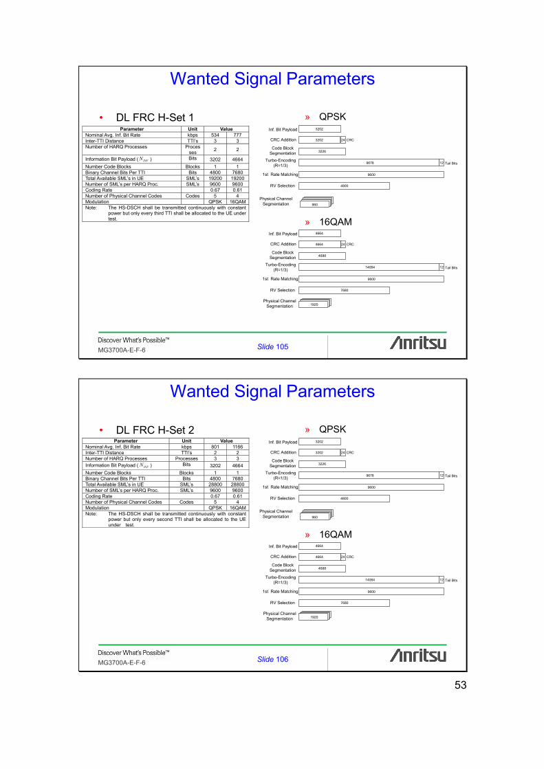
• DL FRC H-Set 1 » QPSK
» 16QAM
Parameter Unit Value Nominal Avg. Inf. Bit Rate kbps 534 777 Inter-TTI Distance TTI’s 3 3 Number of HARQ Processes Proces
ses 2 2
Information Bit Payload ( INFN ) Bits 3202 4664 Number Code Blocks Blocks 1 1 Binary Channel Bits Per TTI Bits 4800 7680 Total Available SML’s in UE SML’s 19200 19200Number of SML’s per HARQ Proc. SML’s 9600 9600 Coding Rate 0.67 0.61 Number of Physical Channel Codes Codes 5 4 Modulation QPSK 16QAMNote: The HS-DSCH shall be transmitted continuously with constant
power but only every third TTI shall be allocated to the UE under test.
Inf. Bit Payload
CRC Addition
Turbo-Encoding(R=1/3)
3202
Code BlockSegmentation
1st Rate Matching 9600
Tail Bits129678
3226
CRC243202
RV Selection 4800
Physical ChannelSegmentation 960
Inf. Bit Payload
CRC Addition
Turbo-Encoding(R=1/3)
4664
Code BlockSegmentation
1st Rate Matching 9600
Tail Bits1214064
4688
CRC244664
RV Selection 7680
1920Physical Channel
Segmentation
Slide 106MG3700A-E-F-6
Wanted Signal Parameters
• DL FRC H-Set 2 » QPSK
» 16QAM
Parameter Unit Value Nominal Avg. Inf. Bit Rate kbps 801 1166 Inter-TTI Distance TTI’s 2 2 Number of HARQ Processes Processes 3 3 Information Bit Payload ( INFN ) Bits 3202 4664 Number Code Blocks Blocks 1 1 Binary Channel Bits Per TTI Bits 4800 7680 Total Available SML’s in UE SML’s 28800 28800Number of SML’s per HARQ Proc. SML’s 9600 9600 Coding Rate 0.67 0.61 Number of Physical Channel Codes Codes 5 4 Modulation QPSK 16QAMNote: The HS-DSCH shall be transmitted continuously with constant
power but only every second TTI shall be allocated to the UE under test.
Inf. Bit Payload
CRC Addition
Turbo-Encoding(R=1/3)
3202
Code BlockSegmentation
1st Rate Matching 9600
Tail Bits129678
3226
CRC243202
RV Selection 4800
Physical ChannelSegmentation 960
Inf. Bit Payload
CRC Addition
Turbo-Encoding(R=1/3)
4664
Code BlockSegmentation
1st Rate Matching 9600
Tail Bits1214064
4688
CRC244664
RV Selection 7680
1920Physical Channel
Segmentation
54
Slide 107MG3700A-E-F-6
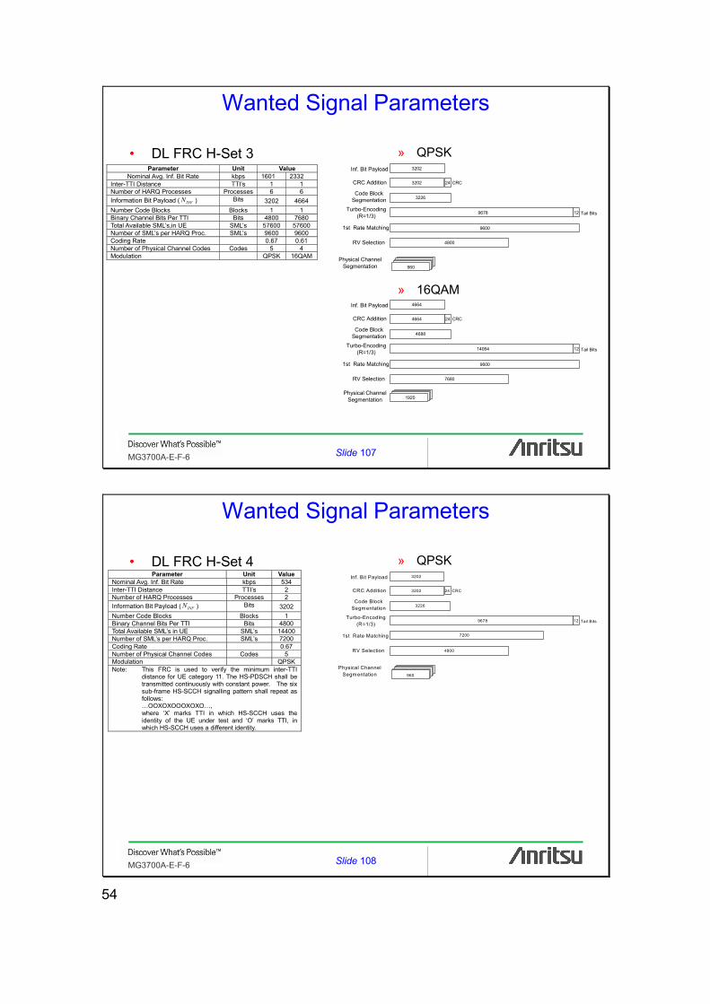
Wanted Signal Parameters
• DL FRC H-Set 3 » QPSK
» 16QAM
Parameter Unit Value Nominal Avg. Inf. Bit Rate kbps 1601 2332
Inter-TTI Distance TTI’s 1 1 Number of HARQ Processes Processes 6 6 Information Bit Payload ( INFN ) Bits 3202 4664 Number Code Blocks Blocks 1 1 Binary Channel Bits Per TTI Bits 4800 7680 Total Available SML’s,in UE SML’s 57600 57600 Number of SML’s per HARQ Proc. SML’s 9600 9600 Coding Rate 0.67 0.61 Number of Physical Channel Codes Codes 5 4 Modulation QPSK 16QAM
Inf. Bit Payload
CRC Addition
Turbo-Encoding(R=1/3)
3202
Code BlockSegmentation
1st Rate Matching 9600
Tail Bits129678
3226
CRC243202
RV Selection 4800
Physical ChannelSegmentation 960
Inf. Bit Payload
CRC Addition
Turbo-Encoding(R=1/3)
4664
Code BlockSegmentation
1st Rate Matching 9600
Tail Bits1214064
4688
CRC244664
RV Selection 7680
1920Physical Channel
Segmentation
Slide 108MG3700A-E-F-6
Wanted Signal Parameters
• DL FRC H-Set 4 » QPSKParameter Unit Value
Nominal Avg. Inf. Bit Rate kbps 534 Inter-TTI Distance TTI’s 2 Number of HARQ Processes Processes 2 Information Bit Payload ( INFN ) Bits 3202 Number Code Blocks Blocks 1 Binary Channel Bits Per TTI Bits 4800 Total Available SML’s in UE SML’s 14400Number of SML’s per HARQ Proc. SML’s 7200 Coding Rate 0.67 Number of Physical Channel Codes Codes 5 Modulation QPSKNote: This FRC is used to verify the minimum inter-TTI
distance for UE category 11. The HS-PDSCH shall be transmitted continuously with constant power. The six sub-frame HS-SCCH signalling pattern shall repeat as follows: …OOXOXOOOXOXO…, where ‘X’ marks TTI in which HS-SCCH uses the identity of the UE under test and ‘O’ marks TTI, in which HS-SCCH uses a different identity.
Inf. Bit Payload
CRC Addition
Turbo-Encoding(R=1/3)
3202
Code BlockSegmentation
1st Rate Matching
Tail Bits129678
3226
CRC243202
RV Selection 4800
Physical ChannelSegmentation 960
7200

55
Slide 109MG3700A-E-F-6
Wanted Signal Parameters
• DL FRC H-Set 5 » QPSKParameter Unit Value
Nominal Avg. Inf. Bit Rate kbps 801 Inter-TTI Distance TTI’s 1 Number of HARQ Processes Processes 3 Information Bit Payload ( INFN ) Bits 3202 Number Code Blocks Blocks 1 Binary Channel Bits Per TTI Bits 4800 Total Available SML’s in UE SML’s 28800Number of SML’s per HARQ Proc. SML’s 9600 Coding Rate 0.67 Number of Physical Channel Codes Codes 5 Modulation QPSKNote: This FRC is used to verify the minimum inter-TTI
distance for UE category 12. The HS-PDSCH shall be transmitted continuously with constant power. The six sub-frame HS-SCCH signalling pattern shall repeat as follows: …OOXXXOOOXXXO…, where ‘X’ marks TTI in which HS-SCCH uses the identity of the UE under test and ‘O’ marks TTI, in which HS-SCCH uses a different identity.
Inf. Bit Payload
CRC Addition
Turbo-Encoding(R=1/3)
3202
Code BlockSegmentation
1st Rate Matching 9600
Tail Bits129678
3226
CRC243202
RV Selection 4800
Physical ChannelSegmentation 960
Slide 110MG3700A-E-F-6
Wanted Signal Parameters
• DL FRC H-Set 6 » QPSK
» 16QAM
Parameter Unit Value Nominal Avg. Inf. Bit Rate kbps 3219 4689 Inter-TTI Distance TTI’s 1 1 Number of HARQ Processes Proces
ses 6 6
Information Bit Payload ( INFN ) Bits 6438 9377 Number Code Blocks Blocks 2 2 Binary Channel Bits Per TTI Bits 9600 15360Total Available SML’s in UE SML’s 115200 115200Number of SML’s per HARQ Proc. SML’s 19200 19200Coding Rate 0.67 0.61 Number of Physical Channel Codes Codes 10 8 Modulation QPSK 16QAM
4800
9600
129693
Inf. Bit Payload
CRC Addition
Turbo-Encoding(R=1/3)
6438
Code BlockSegmentation
1st Rate Matching 9600
Tail Bits129693
3231
CRC246438
RV Selection 4800
Physical ChannelSegmentation
960
4800
9600
129693
Inf. Bit Payload
CRC Addition
Turbo-Encoding(R=1/3)
9377
Code BlockSegmentation
1st Rate Matching 9600
Tail Bits1214103
4701
CRC249377
RV Selection 7680
Physical ChannelSegmentation
1920
56
Slide 111MG3700A-E-F-6
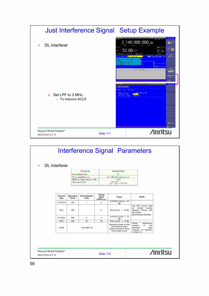
Just Interference Signal Setup Example
• DL Interferer
» Set LPF to 3 MHz.– To improve ACLR
Slide 112MG3700A-E-F-6
Interference Signal Parameters
• DL Interferer
Channel Type
Spreading Factor
Channelization Code
Timing offset
(x256Tchip) Power NOTE
P-CCPCH 256 1 0 P-CCPCH_Ec/Ior = -10 dB
SCH 256 - 0 SCH_Ec/Ior = -10 dB
The SCH power shall be divided equally between Primary and Secondary Synchronous channels
P-CPICH 256 0 0 P-CPICH_Ec/Ior = -10 dB
PICH 256 16 16 PICH_Ec/Ior = -15 dB
OCNS See table C.6
Necessary power so that total transmit power
spectral density of Node B (Ior) adds to one
OCNS interference consists of the dedicated data channels. as specified in Table C.6.
57
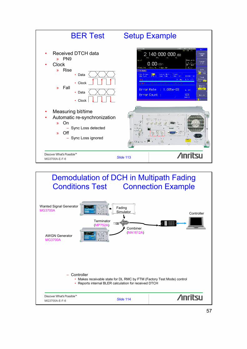
Slide 113MG3700A-E-F-6
BER Test Setup Example
• Received DTCH data» PN9
• Clock» Rise
• Data
• Clock» Fall
• Data
• Clock
• Measuring bit/time• Automatic re-synchronization
» On– Sync Loss detected
» Off– Sync Loss ignored
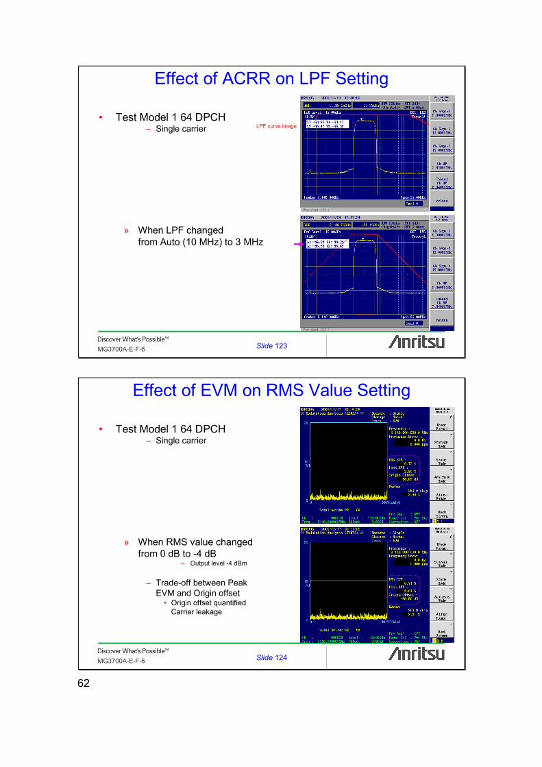
Slide 114MG3700A-E-F-6
AWGN GeneratorMG3700A
Controller
Wanted Signal GeneratorMG3700A
Demodulation of DCH in Multipath Fading Conditions Test Connection Example
– Controller• Makes receivable state for DL RMC by FTM (Factory Test Mode) control• Reports internal BLER calculation for received DTCH
FadingSimulator
Combiner(MA1612A)
Terminator(MP752A)
32
1
65
4
98
7
#0
*

58
Slide 115MG3700A-E-F-6
AWGN Setup Example
• AWGN» Ioc [dBm/3.84MHz]
Slide 116MG3700A-E-F-6
– Controller• Makes maximum transmitting power state by FTM (Factory Test Mode) control
Controller
Transmit Intermodulation TestConnection Example
Circulator
Spectrum Analyzer
CW GeneratorMG3700A
32
1
65
4
98
7
#0
*

59
Slide 117MG3700A-E-F-6
Interference CW Signal Setup Example
• Modulation Off
Slide 118MG3700A-E-F-6
Repeater Test
MG3700A
InterferenceSignalGenerator
Signal AnalyzerMG3700AModulation accuracy10
Spectrum AnalyzerAdjacent Channel Rejection Ratio (ACRR)13
Spectrum AnalyzerCirculatorOutput intermodulation12
Spectrum AnalyzerInput intermodulation11
Spectrum AnalyzerUnwanted emission9Spectrum AnalyzerOut of band gain8Frequency CounterFrequency stability7Power MeterOutput power6
OthersSignalGeneratorTest
TS 25.143 (Release 7)3GPP

60
Slide 119MG3700A-E-F-6
Basic Tests Connection Example
• Output power» Maximum output power
• Frequency stability• Out of band gain• Unwanted emission
» Spectrum emission mask» Spurious emissions
• Modulation accuracy» EVM» PCDE
• Input intermodulation» 2-tone intermodulation
Signal GeneratorMG3700A
Reference clock TX TesterMS8609A
Slide 120MG3700A-E-F-6
Output Intermodulation TestConnection Example
Circulator
Signal GeneratorMG3700A
Reference clockSpectrum Analyzer(TX Tester)MS8609A
Interference Signal GeneratorMG3700A

61
Slide 121MG3700A-E-F-6
Downlink Signal Setup Example
Test– Output power– Frequency stability– Out of band gain– Unwanted emission– EVM– Output intermodulation– ACRR
• Test Model 1• Single carrier• Multi-carrier
» Set the LPF correctly.» Tune the RMS value
correctly.– To improve ACRR, EVM
for– Out of band gain– Unwanted emission– EVM– Output intermodulation– ACRR
Slide 122MG3700A-E-F-6
Effect of EVM on LPF Setting
• Test Model 1 64 DPCH– Single carrier
» When LPF changedfrom Auto (10 MHz) to 3 MHz
62
Slide 123MG3700A-E-F-6
Effect of ACRR on LPF Setting
• Test Model 1 64 DPCH– Single carrier
» When LPF changedfrom Auto (10 MHz) to 3 MHz
LPF curve image
Slide 124MG3700A-E-F-6
Effect of EVM on RMS Value Setting
• Test Model 1 64 DPCH– Single carrier
» When RMS value changedfrom 0 dB to -4 dB
– Output level -4 dBm
– Trade-off between Peak EVM and Origin offset
• Origin offset quantified Carrier leakage

63
Slide 125MG3700A-E-F-6
Effect of ACRR on RMS Value Setting
• Test Model 1 64 DPCH– Single carrier
» When RMS value changedfrom 0 dB to -1 dB
– Output level -2 dBm
...≈ -1 dB
...≈ +1 dB
Slide 126MG3700A-E-F-6
Downlink Signal Setup Example
Test– PCDE
• Test Model 3

64
Slide 127MG3700A-E-F-6
Downlink Signal Parameters
• Test Model 1Type Number of
Channels Fraction of Power (%)
Level setting (dB)
Channelization Code
Timing offset (x256Tchip)
P-CCPCH+SCH 1 10 -10 1 0 Primary CPICH 1 10 -10 0 0
PICH 1 1.6 -18 16 120 S-CCPCH containing
PCH (SF=256) 1 1.6 -18 3 0
DPCH (SF=128)
16/32/64 76.8 in total see table 6.2 see table 6.2 see table 6.2
4 91 -17 9 7 -18
12 32 -20 14 21 -17 19 29 -19 22 59 -21 26 22 -19 28 138 -23 34 31 -22 36 17 -19 40 9 -24 44 69 -23 49 49 -22 53 20 -19 56 57 -22 61 121 -21 63 127 -18 66 114 -19 71 100 -22 76 76 -21 80 141 -19 84 82 -21 87 64 -19 91 149 -21 95 87 -20 99 98 -25
105 46 -25 110 37 -25 116 87 -24 118 149 -22 122 85 -20 126 69 -15
Code Timing offset (x256Tchip)
Level settings (dB) (16 codes)
Level settings (dB) (32 codes)
Level settings (dB) (64 codes)
2 86 -10 -13 -16 11 134 -12 -13 -16 17 52 -12 -14 -16 23 45 -14 -15 -17 31 143 -11 -17 -18 38 112 -13 -14 -20 47 59 -17 -16 -16 55 23 -16 -18 -17 62 1 -13 -16 -16 69 88 -15 -19 -19 78 30 -14 -17 -22 85 18 -18 -15 -20 94 30 -19 -17 -16
102 61 -17 -22 -17 113 128 -15 -20 -19 119 143 -9 -24 -21
7 83 -20 -19 13 25 -18 -21 20 103 -14 -18 27 97 -14 -20 35 56 -16 -24 41 104 -19 -24 51 51 -18 -22 58 26 -17 -21 64 137 -22 -18 74 65 -19 -20 82 37 -19 -17 88 125 -16 -18 97 149 -18 -19
108 123 -15 -23 117 83 -17 -22 125 5 -12 -21
Slide 128MG3700A-E-F-6
Downlink Signal Parameters
• Test Model 3Type Number of
Channels Fraction of Power (%)
16/32
Level settings (dB) 16/32
Channelization Code
Timing offset (x256Tchip)
P-CCPCH+SCH 1 12,6/7,9 -9 / -11 1 0 Primary CPICH 1 12,6/7,9 -9 / -11 0 0
PICH 1 5/1.6 -13/-18 16 120 S-CCPCH containing
PCH (SF=256) 1 5/1.6 -13/-18 3 0
DPCH (SF=256)
16/32 63,7/80,4 in total
see table 6.5 see table 6.5 see table 6.5
Code Toffset Level settings (dB) (16 codes)
Level settings dB) (32 codes)
64 86 -14 -16 69 134 -14 -16 74 52 -14 -16 78 45 -14 -16 83 143 -14 -16 89 112 -14 -16 93 59 -14 -16 96 23 -14 -16 100 1 -14 -16 105 88 -14 -16 109 30 -14 -16 111 18 -14 -16 115 30 -14 -16 118 61 -14 -16 122 128 -14 -16 125 143 -14 -16 67 83 -16 71 25 -16 76 103 -16 81 97 -16 86 56 -16 90 104 -16 95 51 -16 98 26 -16 103 137 -16 108 65 -16 110 37 -16 112 125 -16 117 149 -16 119 123 -16 123 83 -16 126 5 -16

65
Slide 129MG3700A-E-F-6
2-tone Signal Setup Example
Test– Input intermodulation
License option MX370104A
Slide 130MG3700A-E-F-6
2-tone Signal Setup Example
• Two CW carriers with 3.5 MHz offset
» Set the LPF correctly.» Tune the RMS value
correctly.– To improve IMD

66
Slide 131MG3700A-E-F-6
Effect of IMD on RMS Value Setting
• Two CW carriers with 3.5 MHz offset
– RBW 1 MHz
» When RMS value changedfrom 0 dB to -4 dB
– Output level -4 dBmTest requirementat Repeater output
Slide 132MG3700A-E-F-6
Interference Signal Setup Example
• Test Model 1» Select any one of:
» Set LPF to 3 MHz.– To improve ACLR

67
Slide 133MG3700A-E-F-6
Peak Clipping Technique
• Standard Test Model 1 patterns are I/Q waveforms without peak clipping.
» EVM gives best performance.• Peak clipping affects the spectral regrowth and EVM because of
changing CCDF curves.» It can improve the spectral regrowth.
Spectrum simulated by FFT
Slide 134MG3700A-E-F-6
Peak Clipping Type
Vector Scalar
∑I/Q mapping at chip rateper channel Clipping
(pre-filter)BasebandFIR filter
Clipping(post-filter)
Frequencyshift
I/Q mapping at chip rateper channelI/Q mapping at chip rate
per channel
∑I/Q mapping at chip rateper channel Clipping
(pre-filter)BasebandFIR filter
Clipping(post-filter)
Frequencyshift
I/Q mapping at chip rateper channelI/Q mapping at chip rate
per channel
:
:
I/Q waveformdata
Oversamplingwith Root Nyquist 0.22 roll-off
I
Q
I
Q
100%
ReferencePeak amplitude
Index %
Index
dB
Index %Index %
ReferencePeak amplitude
100%
ReferenceRMS amplitude Index dB
ReferenceRMS amplitude
Index dB
22
22
amplitude RMS
maxamplitudePeak
QI
QI
+=
+=( )
2amplitude RMS
,maxamplitudePeak 22
maxmax
QI
QI
+=
=

68
Slide 135MG3700A-E-F-6
Peak Clipping Modeling
∑Test Model 1 64 DPCHI/Q mapping at chip rate Clipping
(pre-filter)BasebandFIR filter
Test Model 1 64 DPCHI/Q mapping at chip rateTest Model 1 64 DPCH
I/Q mapping at chip rate
68 channels
I/Q waveformdata
4 × OversamplingVector 50% (-6 dB)
Non-clipping case
ReferencePeak amplitude
Slide 136MG3700A-E-F-6
Peak Clipping Modeling
∑I/Q mapping at chip rateper channel Clipping
(post-filter)BasebandFIR filter
I/Q mapping at chip rateper channelTest Model 1 64 DPCH
I/Q mapping at chip rate
68 channels
I/Q waveformdata
4 × Oversampling Vector 50% (-6 dB)
ReferencePeak amplitude

69
Slide 137MG3700A-E-F-6
Effect of CCDF & Spectrum on Peak Clipping
• Pre-filter clipping can improve spectral regrowth because of lower PAR. It is a trade-off with EVM.
• Post-filter clipping can simulate spectral regrowth of nonlinear devices.
Non-clipping
Vector(Pre-filter)50% clipping
Vector(Post-filter)50% clipping
7.61 dB
Vector(Pre-filter)50% clipping Non-clipping
Vector(Post-filter)50% clipping
Slide 138MG3700A-E-F-6
Uplink Signal Setup Example
Test– Output power– Frequency stability– Out of band gain– Unwanted emission– EVM– PCDE– ACRR
• UL RMC 12.2 kbps

70
Slide 139MG3700A-E-F-6
UL RMC 12.2 kbps EVM, PCDE, ACRR
DPCCH
DPDCH
Slide 140MG3700A-E-F-6
Uplink Signal Parameters
• UL RMC 12.2 kbps
Parameter Unit Level Information bit rate kbps 12.2
DPDCH kbps 60 DPCCH kbps 15 DPCCH Slot Format #i - 0 DPCCH/DPDCH power ratio dB -5.46 TFCI - On Repetition % 23 NOTE: Slot Format #2 is used for closed loop tests in subclause 8.6.2. Slot Format #2 and #5 are used for site selection diversity transmission
tests in subclause 8.6.3
Parameters DTCH DCCH Transport Channel Number 1 2 Transport Block Size 244 100 Transport Block Set Size 244 100 Transmission Time Interval 20 ms 40 ms Type of Error Protection Convolution Coding Convolution Coding Coding Rate 1/3 1/3 Rate Matching attribute 256 256 Size of CRC 16 12

71
Slide 141MG3700A-E-F-6
UL RMC 12.2 kbps Same setupHSPA or Limited W-CDMA IQproducer
• Created sample rate– 3 × Oversampling
DPCCH: -5.46 dBDPDCH: 0 dB
License option MX370101A
Non-license
Slide 142MG3700A-E-F-6
Additional Information
• DL Test Models for BS Transmitter Test 143– Explore 3GPP TS 25.141 subclause 6.1.1
• UL RMC for UE Transmitter Test 154– Explore 3GPP TS 34.121
• Number of Created Frames 171– Extract from operation manual for MX370101A HSPA IQproducer
• Transmitter/Receiver Requirements for HSPA UE 174– Refer to chapter 11 in the following reference book.
• Principal parts of UE transmitter and receiver requirements withemphasis on new aspects introduced using HSDPA/HSUPA
Reference– H.Holma and A.Toskala (eds) (2006), HSDPA/HSUPA for UMTS, John
Wiley & Sons, Chichester, UK

72
Slide 143MG3700A-E-F-6
DL Test Models for BS Transmitter Test
• Test Model 1Test– OBW– Spectrum emission mask– ACLR– Spurious emissions– Transmit intermodulation– Maximum output power– Total power dynamic range– Frequency error– EVM
Type Number of Channels
Fraction of Power (%)
Level setting (dB)
Channelization Code
Timing offset (x256Tchip)
P-CCPCH+SCH 1 10 -10 1 0 Primary CPICH 1 10 -10 0 0
PICH 1 1.6 -18 16 120 S-CCPCH containing
PCH (SF=256) 1 1.6 -18 3 0
DPCH (SF=128)
16/32/64 76.8 in total see table 6.2 see table 6.2 see table 6.2
4 91 -17 9 7 -18
12 32 -20 14 21 -17 19 29 -19 22 59 -21 26 22 -19 28 138 -23 34 31 -22 36 17 -19 40 9 -24 44 69 -23 49 49 -22 53 20 -19 56 57 -22 61 121 -21 63 127 -18 66 114 -19 71 100 -22 76 76 -21 80 141 -19 84 82 -21 87 64 -19 91 149 -21 95 87 -20 99 98 -25
105 46 -25 110 37 -25 116 87 -24 118 149 -22 122 85 -20 126 69 -15
Code Timing offset (x256Tchip)
Level settings (dB) (16 codes)
Level settings (dB) (32 codes)
Level settings (dB) (64 codes)
2 86 -10 -13 -16 11 134 -12 -13 -16 17 52 -12 -14 -16 23 45 -14 -15 -17 31 143 -11 -17 -18 38 112 -13 -14 -20 47 59 -17 -16 -16 55 23 -16 -18 -17 62 1 -13 -16 -16 69 88 -15 -19 -19 78 30 -14 -17 -22 85 18 -18 -15 -20 94 30 -19 -17 -16
102 61 -17 -22 -17 113 128 -15 -20 -19 119 143 -9 -24 -21
7 83 -20 -19 13 25 -18 -21 20 103 -14 -18 27 97 -14 -20 35 56 -16 -24 41 104 -19 -24 51 51 -18 -22 58 26 -17 -21 64 137 -22 -18 74 65 -19 -20 82 37 -19 -17 88 125 -16 -18 97 149 -18 -19
108 123 -15 -23 117 83 -17 -22 125 5 -12 -21
Slide 144MG3700A-E-F-6
Test Model 1 for BS Transmitter Test
» For more information about EVM, ACLR and Peak clipping, see Downlink Signal parts in Repeater Test.

73
Slide 145MG3700A-E-F-6
DL Test Models for BS Transmitter Test
• Test Model 2Test– Output power dynamics– CPICH power accuracy
Type Number of Channels
Fraction of Power (%)
Level setting (dB)
Channelization Code
Timing offset (x256Tchip)
P-CCPCH+SCH 1 10 -10 1 0 Primary CPICH 1 10 -10 0 0
PICH 1 5 -13 16 120 S-CCPCH containing
PCH (SF=256) 1 5 -13 3 0
DPCH (SF=128)
3 2 x 10,1 x 50 2 x –10, 1 x –3 24, 72, 120
1, 7, 2
Pmax -3 dB
≤-28 dB
Slide 146MG3700A-E-F-6
DL Test Models for BS Transmitter Test
• Test Model 3Test– Peak code domain error
Type Number of Channels
Fraction of Power (%)
16/32
Level settings (dB) 16/32
Channelization Code
Timing offset (x256Tchip)
P-CCPCH+SCH 1 12,6/7,9 -9 / -11 1 0 Primary CPICH 1 12,6/7,9 -9 / -11 0 0
PICH 1 5/1.6 -13/-18 16 120 S-CCPCH containing
PCH (SF=256) 1 5/1.6 -13/-18 3 0
DPCH (SF=256)
16/32 63,7/80,4 in total
see table 6.5 see table 6.5 see table 6.5
Code Toffset Level settings
(dB) (16 codes) Level settings dB) (32 codes)
64 86 -14 -16 69 134 -14 -16 74 52 -14 -16 78 45 -14 -16 83 143 -14 -16 89 112 -14 -16 93 59 -14 -16 96 23 -14 -16 100 1 -14 -16 105 88 -14 -16 109 30 -14 -16 111 18 -14 -16 115 30 -14 -16 118 61 -14 -16 122 128 -14 -16 125 143 -14 -16 67 83 -16 71 25 -16 76 103 -16 81 97 -16 86 56 -16 90 104 -16 95 51 -16 98 26 -16 103 137 -16 108 65 -16 110 37 -16 112 125 -16 117 149 -16 119 123 -16 123 83 -16 126 5 -16

74
Slide 147MG3700A-E-F-6
DL Test Models for BS Transmitter Test
• Test Model 4Test– EVM (at Pmax –18 dB)– Total power dynamic range
(at Pmax –18 dB)– Frequency error
(at Pmax –18 dB)Type Number of
Channels Fraction of Power (%)
Level setting (dB)
Channelization Code
Timing offset
PCCPCH+SCH when Primary
CPICH is disabled
1 1.6 -18 1 0
PCCPCH+SCH when Primary
CPICH is enabled
1 0.8 -21 1 0
Primary CPICH1 1 0.8 -21 0 0 Note 1: The CPICH channel is optional.
Slide 148MG3700A-E-F-6
Test Model 4 for BS Transmitter Test
Type Number of Channels
Fraction of Power (%)
Level setting (dB)
Channelization Code
Timing offset
PCCPCH+SCH when Primary
CPICH is disabled
1 1.6 -18 1 0
PCCPCH+SCH when Primary
CPICH is enabled
1 0.8 -21 1 0
Primary CPICH1 1 0.8 -21 0 0 Note 1: The CPICH channel is optional.
Non-license

75
Slide 149MG3700A-E-F-6
DL Test Models for BS Transmitter Test
• Test Model 5Test– EVM for HSDPA
Type Number of Channels
Fraction of Power (%)
Level setting (dB)
Channelization Code
Timing offset (x256Tchip)
P-CCPCH+SCH 1 7.9 -11 1 0 Primary CPICH 1 7.9 -11 0 0
PICH 1 1.3 -19 16 120 S-CCPCH containing
PCH (SF=256) 1 1.3 -19 3 0
DPCH (SF=128)
30/14/6(*) 14/14.2/14.4 in total
see table 6.b see table 6.b see table 6.b
HS-SCCH 2 4 in total see table 6.c see table 6.c see table 6.cHS-PDSCH (16QAM) 8/4/2(*) 63.6/63.4/63.2
in total see table 6.d see table 6.d see table 6.d
Note *: 2 HS-PDSCH shall be taken together with 6 DPCH, 4 HS-PDSCH shall be taken with 14 DPCH, and 8 HS-PDSCH shall be taken together with 30 DPCH.
Code (SF=128)
Timing offset (x256Tchip)
Level settings (dB) (30 codes)
Level settings (dB) (14 codes)
Level settings (dB) (6 codes)
15 86 -20 -17 -17 23 134 -20 -19 -15 68 52 -21 -19 -15 76 45 -22 -20 -18 82 143 -24 -18 -16 90 112 -21 -20 -17 5 59 -23 -25 11 23 -25 -23 17 1 -23 -20 27 88 -26 -22 64 30 -24 -21 72 18 -22 -22 86 30 -24 -19 94 61 -28 -20 3 128 -27 7 143 -26 13 83 -27 19 25 -25 21 103 -21 25 97 -21 31 56 -23 66 104 -26 70 51 -25 74 26 -24 78 137 -27 80 65 -26 84 37 -23 88 125 -25 89 149 -22 92 123 -24
Code
(SF=128) Timing offset
(x256Tchip) Level settings
(dB) 9 0 -15
29 0 -21 Code
(SF=16) Timing offset
(x256Tchip) Level settings(dB) (8 codes)
Level settings (dB) (4 codes)
Level settings (dB) (2 codes)
4 0 -11 -8 -5 5 0 -11 -8 6 0 -11 7 0 -11
12 0 -11 -8 -5 13 0 -11 -8 14 0 -11 15 0 -11
Slide 150MG3700A-E-F-6
Test Model 5 for BS Transmitter Test
HS-PDSCHHS-PDSCH

76
Slide 151MG3700A-E-F-6
DPCH Structure of DL Test Models
Slot Format
Channel Bit
Channel Symbol
SF Bits/Frame Bits/ Slot
DPDCH Bits/Slot DPCCH Bits/Slot
#I Rate (kbps)
Rate (ksps)
DPDCH DPCCH TOT NData1 Ndata2 NTFCI NTPC Npilot
10 60 30 128 450 150 600 40 6 24 0 2 8 6 30 15 256 150 150 300 20 2 8 0 2 8
One radio frame, Tf = 10 ms
TPC NTPC bits
Slot #0 Slot #1 Slot #i Slot #14
Tslot = 2560 chips, 10*2k bits (k=0..7)
Data2Ndata2 bits
DPDCHTFCI
NTFCI bitsPilot
Npilot bitsData1
Ndata1 bits
DPDCH DPCCH DPCCH
Test Model1, 2, 5
3
PN9 (Seed for PN sequence at start of each frame: Channelization code)
Alternate 00/11 Npilot = 8 Symbol # 0 1 2 3
Slot #0 1 2 3 4 5 6 7 8 9
10 11 12 13 14
11 11 11 11 11 11 11 11 11 11 11 11 11 11 11
11 00 01 00 10 11 11 10 01 11 01 10 10 00 00
11 11 11 11 11 11 11 11 11 11 11 11 11 11 11
101001000110000010110111001111
Slide 152MG3700A-E-F-6
HS-SCCH, HS-PDSCH Structure of DL Test Model 5
• HS-SCCH
• HS-PDSCH
Slot #0 Slot#1 Slot #2
Tslot = 2560 chips, 40 bits
DataNdata1 bits
1 subframe: T f = 2 ms
Slot #0 Slot#1 Slot #2
Tslot = 2560 chips, M*10*2 k bits (k=4)
Data Ndata1 bits
1 subframe: Tf = 2 ms
Slot format #i Channel Bit Rate (kbps)
Channel Symbol
Rate (ksps)
SF Bits/ HS-DSCH
subframe
Bits/ Slot Ndata
0(QPSK) 480 240 16 960 320 320 1(16QAM) 960 240 16 1920 640 640
1 frame: 10 ms = 5× 2 ms
PN9 (Seed for PN sequence at start of each frame: 23× Channelization code)
PN9 (Seed for PN sequence at start of each frame: Channelization code)

77
Slide 153MG3700A-E-F-6
DL Test Models for BS Transmitter TestCCDF Simulation
Slide 154MG3700A-E-F-6
UL RMC for UE Transmitter Test
• UL RMC 12.2 kbps Test– Maximum output power– Frequency error– OBW– Spectrum emission mask– ACLR– Spurious emissions– Transmit intermodulation– EVM– PCDE
Type of User Information
User bit rate DL DPCH symbol rate
UL DPCH bit rate
Remarks
12,2 kbps reference
measurement channel
12,2 kbps 30 ksps 60 kbps Standard Test
Parameter Unit Level Information bit rate kbps 12.2
DPDCH kbps 60 DPCCH kbps 15 DPCCH Slot Format #i - 0 DPCCH/DPDCH power ratio dB -5.46 TFCI - On Repetition % 23 NOTE: Slot Format #2 is used for closed loop tests in subclause 8.6.2. Slot Format #2 and #5 are used for site selection diversity transmission
tests in subclause 8.6.3
Parameters DTCH DCCH Transport Channel Number 1 2 Transport Block Size 244 100 Transport Block Set Size 244 100 Transmission Time Interval 20 ms 40 ms Type of Error Protection Convolution Coding Convolution Coding Coding Rate 1/3 1/3 Rate Matching attribute 256 256 Size of CRC 16 12
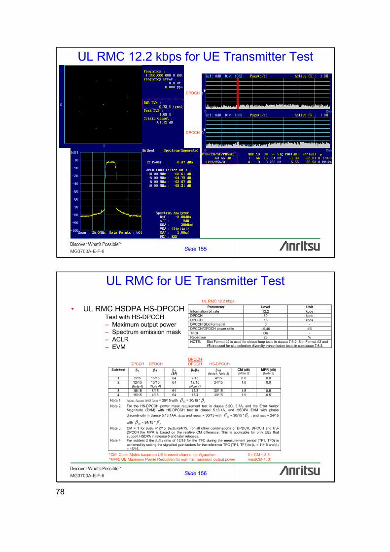
78
Slide 155MG3700A-E-F-6
UL RMC 12.2 kbps for UE Transmitter Test
DPCCH
DPDCH
Slide 156MG3700A-E-F-6
UL RMC for UE Transmitter Test
• UL RMC HSDPA HS-DPCCHTest with HS-DPCCH– Maximum output power– Spectrum emission mask– ACLR– EVM
Parameter Level Unit Information bit rate 12,2 kbps DPDCH 60 kbps DPCCH 15 kbps DPCCH Slot Format #i 0 - DPCCH/DPDCH power ratio −5,46 dB TFCI On - Repetition 23 % NOTE: Slot Format #2 is used for closed loop tests in clause 7.6.2. Slot Format #2 and
#5 are used for site selection diversity transmission tests in subclause 7.6.3.
Sub-test βc βd βd (SF)
βc/βd
βHS (Note1, Note 2)
CM (dB) (Note 3)
MPR (dB) (Note 3)
1 2/15 15/15 64 2/15 4/15 0.0 0.0 2 12/15
(Note 4) 15/15
(Note 4) 64 12/15
(Note 4) 24/15 1.0 0.0
3 15/15 8/15 64 15/8 30/15 1.5 0.5 4 15/15 4/15 64 15/4 30/15 1.5 0.5
Note 1: ∆ACK, ∆NACK and ∆CQI = 30/15 with hsβ = 30/15 * cβ Note 2: For the HS-DPCCH power mask requirement test in clause 5.2C, 5.7A, and the Error Vector
Magnitude (EVM) with HS-DPCCH test in clause 5.13.1A, and HSDPA EVM with phase discontinuity in clause 5.13.1AA, ∆ACK and ∆NACK = 30/15 with hsβ = 30/15 * cβ , and ∆CQI = 24/15
with hsβ = 24/15 * cβ
Note 3: CM = 1 for βc/βd =12/15, βhs/βc=24/15. For all other combinations of DPDCH, DPCCH and HS-DPCCH the MPR is based on the relative CM difference. This is applicable for only UEs that support HSDPA in release 6 and later releases.
Note 4: For subtest 2 the βc/βd ratio of 12/15 for the TFC during the measurement period (TF1, TF0) is achieved by setting the signalled gain factors for the reference TFC (TF1, TF1) to βc = 11/15 and βd = 15/15.
HS-DPCCHDPCCH DPDCHDPCCHDPDCH
*CM: Cubic Metric based on UE transmit channel configuration 0 ≤ CM ≤ 3.5*MPR: UE Maximum Power Reduction for nominal maximum output power max(CM-1, 0)
UL RMC 12.2 kbps

79
Slide 157MG3700A-E-F-6
UL RMC for UE Transmitter Test
• UL RMC HSUPA E-DCHTest with HS-DPCCH and E-DCH– Maximum output power– Spectrum emission mask– ACLR– EVM
TrCH type E-DCH TTI 10ms (alt. 2ms) (NOTE) Coding type TC
Layer 1
CRC, bit 24 NOTE: The support of 2ms TTI depends on the UE category UE E-DPDCH Physical
Layer category Number of processes
TTI Max Data Rate
1 4 10 ms 0.7296 Mbps 2 4 10 ms 1.4592 Mbps 2 8 2 ms 1.4595 Mbps 3 4 10 ms 1.4592 Mbps 4 4 10 ms 2.0 Mbps 4 8 2 ms 2.9185 Mbps 5 4 10 ms 2.0 Mbps 6 4 10 ms 2.0 Mbps 6 8 2 ms 5.76 Mbps
Sub-test
βc βd βd (SF)
βc/βd βHS (Note1)
βec
βed (Note 5) (Note 6)
βed (SF)
βed (Codes)
CM (dB)
(Note 2)
MPR (dB)
(Note 2)
AG Index
(Note 6)
E-TFCI
1 11/15 (Note 3)
15/15 (Note 3)
64 11/15 (Note 3)
22/15 209/225 1309/225 4 1 1.0 0.0 20 75
2 6/15 15/15 64 6/15 12/15 12/15 94/75 4 1 3.0 2.0 12 65 3 15/15 9/15 64 15/9 30/15 30/15 βed1: 47/15
βed2: 47/154 4
2 2.0 1.0 15 94
4 2/15 15/15 64 2/15 4/15 2/15 56/75 4 1 3.0 2.0 17 70 5 15/15
(Note 4)15/15
(Note 4) 64 15/15
(Note 4) 30/15 24/15 134/15 4 1 1.0 0.0 21 80
Note 1: ∆ACK, ∆NACK and ∆CQI = 30/15 with hsβ = 30/15 * cβ .
Note 2: CM = 1 for βc/βd =12/15, βhs/βc=24/15. For all other combinations of DPDCH, DPCCH, HS- DPCCH, E-DPDCH and E-DPCCH the MPR is based on the relative CM difference.
Note 3: For subtest 1 the βc/βd ratio of 11/15 for the TFC during the measurement period (TF1, TF0) is achieved by setting the signalled gain factors for the reference TFC (TF1, TF1) to βc = 10/15 and βd = 15/15.
Note 4: For subtest 5 the βc/βd ratio of 15/15 for the TFC during the measurement period (TF1, TF0) is achieved by setting the signalled gain factors for the reference TFC (TF1, TF1) to βc = 14/15 and βd = 15/15.
Note 5: In case of testing by UE using E-DPDCH Physical Layer category 1, Sub-test 3 is omitted according to TS25.306 Table 5.1g. Note 6: βed can not be set directly, it is set by Absolute Grant Value.
DPCCH DPDCH HS-DPCCHDPCCHDPDCH
*CM: Cubic Metric based on UE transmit channel configuration 0 ≤ CM ≤ 3.5*MPR: UE Maximum Power Reduction for nominal maximum output power max(CM-1, 0)
E-DPCCH E-DPDCH
Slide 158MG3700A-E-F-6
Spreading Operation
I Σ
j
cd,1 βd
I+jQ
DPDCH1
Q
cd,3 βd
DPDCH3
cd,5 βd
DPDCH5
cd,2 βd
DPDCH2
cd,4 βd
cc βc
DPCCH
Σ
Sdpch
DPDCH4
cd,6 βd
DPDCH6
I
j
I+jQ
Q
Shs-dpcch chs
HS-DPCCH (If Nmax-dpdch = 0, 1, 3, 5)
chs
HS-DPCCH (If Nmax-dpdch = 2, 4 or 6)
βhs
βhs
Σ Sdpch,n
I+jQ
Sdpch
Shs-dpcch
S
Se-dpch Spreading
Spreading
Spreading
DPCCH DPDCHs
HS-DPCCH
E-DPDCHs E-DPCCH
Σ I+jQ
Se-dpch
ced,1 βed,1
E-DPDCH1
iqed,1
ced,k βed,k
E-DPDCHk
iqed,k
ced,K βed,K
E-DPDCHK
iqed,K
cec βec
E-DPCCH
iqec
.
.
.
.
.
.
.
.
Nmax-dpdch HS-DSCH configured
E-DPDCHk iqed,k
E-DPDCH1 1 E-DPDCH2 j E-DPDCH3 1
0 No/Yes
E-DPDCH4 j E-DPDCH1 j 1 No E-DPDCH2 1 E-DPDCH1 1 1 Yes E-DPDCH2 j
Nmax-dpdch = 1
= 1I
II
Q
Q
Maximum number of simultaneously-configured uplink dedicated channels
DPDCH HS-DPCCH E-DPDCH E-DPCCH Case 1 6 1 - - Case 2 1 1 2 1 Case 3 - 1 4 1
Nmax-dpdch is equal to the largest number of DPDCHsfrom all TFCs in TFCSs, and is not changed byframe-by-frame TFCI change or temporary TFC restrictions.

80
Slide 159MG3700A-E-F-6
Gain Factor β
• Spread signals are weighted by gain factors β.• The β are derived from quantized amplitude ratios β/βc.
License option MX370101A
Computed automatically
Equivalent
Slide 160MG3700A-E-F-6
Gain Factor β
Signalled values for ∆ ACK, ∆ΝACK and ∆CQI
Quantized amplitude ratios Ahs = βhs/βc
8 30/15 7 24/15 6 19/15 5 15/15 4 12/15 3 9/15 2 8/15 1 6/15 0 5/15
Signalled values for βc and βd
Quantized amplitude ratios βc and βd
15 1.0 14 14/15 13 13/15 12 12/15 11 11/15 10 10/15 9 9/15 8 8/15 7 7/15 6 6/15 5 5/15 4 4/15 3 3/15 2 2/15 1 1/15 0 Switch off
Signalled values for ∆ E-DPCCH
Quantized amplitude ratios Aec = βec/βc
8 30/15 7 24/15 6 19/15 5 15/15 4 12/15 3 9/15 2 8/15 1 6/15 0 5/15
Signalled values for ∆ E-DPDCH
Quantized amplitude ratios Aed = βed/βc
29 168/15 28 150/15 27 134/15 26 119/15 25 106/15 24 95/15 23 84/15 22 75/15 21 67/15 20 60/15 19 53/15 18 47/15 17 42/15 16 38/15 15 34/15 14 30/15 13 27/15 12 24/15 11 21/15 10 19/15 9 17/15 8 15/15 7 13/15 6 12/15 5 11/15 4 9/15 3 8/15 2 7/15 1 6/15 0 5/15

81
Slide 161MG3700A-E-F-6
UL RMC HSDPA Quantized Amplitude RatioSub-test 1 Sub-test 2
Sub-test 3 Sub-test 4
For EVM test For EVM test
For EVM test For EVM test
Slide 162MG3700A-E-F-6
UL RMC HSUPA Sub-test 1
E-TFCI TB Size (bits)
E-TFCI TB Size (bits)
E-TFCI TB Size (bits)
E-TFCI TB Size (bits)
E-TFCI TB Size (bits)
0 18 30 389 60 1316 90 4452 120 15051 1 120 31 405 61 1371 91 4636 121 15675 2 124 32 422 62 1428 92 4828 122 16325 3 130 33 440 63 1487 93 5029 123 17001 4 135 34 458 64 1549 94 5237 124 17706 5 141 35 477 65 1613 95 5454 125 18440 6 147 36 497 66 1680 96 5680 126 19204 7 153 37 517 67 1749 97 5915 127 20000 8 159 38 539 68 1822 98 6161 9 166 39 561 69 1897 99 6416
10 172 40 584 70 1976 100 6682 11 180 41 608 71 2058 101 6959 12 187 42 634 72 2143 102 7247 13 195 43 660 73 2232 103 7547 14 203 44 687 74 2325 104 7860 15 211 45 716 75 2421 105 8186 16 220 46 745 76 2521 106 8525 17 229 47 776 77 2626 107 8878 18 239 48 809 78 2735 108 9246 19 249 49 842 79 2848 109 9629 20 259 50 877 80 2966 110 10028 21 270 51 913 81 3089 111 10444 22 281 52 951 82 3217 112 10877 23 293 53 991 83 3350 113 11328 24 305 54 1032 84 3489 114 11797 25 317 55 1074 85 3634 115 12286 26 331 56 1119 86 3784 116 12795 27 344 57 1165 87 3941 117 13325 28 359 58 1214 88 4105 118 13877 29 374 59 1264 89 4275 119 14453
3GPP TS 25.321 Annex B.3

82
Slide 163MG3700A-E-F-6
UL RMC HSUPA Sub-test 2
E-TFCI TB Size (bits)
E-TFCI TB Size (bits)
E-TFCI TB Size (bits)
E-TFCI TB Size (bits)
E-TFCI TB Size (bits)
0 18 30 389 60 1316 90 4452 120 15051 1 120 31 405 61 1371 91 4636 121 15675 2 124 32 422 62 1428 92 4828 122 16325 3 130 33 440 63 1487 93 5029 123 17001 4 135 34 458 64 1549 94 5237 124 17706 5 141 35 477 65 1613 95 5454 125 18440 6 147 36 497 66 1680 96 5680 126 19204 7 153 37 517 67 1749 97 5915 127 20000 8 159 38 539 68 1822 98 6161 9 166 39 561 69 1897 99 6416
10 172 40 584 70 1976 100 6682 11 180 41 608 71 2058 101 6959 12 187 42 634 72 2143 102 7247 13 195 43 660 73 2232 103 7547 14 203 44 687 74 2325 104 7860 15 211 45 716 75 2421 105 8186 16 220 46 745 76 2521 106 8525 17 229 47 776 77 2626 107 8878 18 239 48 809 78 2735 108 9246 19 249 49 842 79 2848 109 9629 20 259 50 877 80 2966 110 10028 21 270 51 913 81 3089 111 10444 22 281 52 951 82 3217 112 10877 23 293 53 991 83 3350 113 11328 24 305 54 1032 84 3489 114 11797 25 317 55 1074 85 3634 115 12286 26 331 56 1119 86 3784 116 12795 27 344 57 1165 87 3941 117 13325 28 359 58 1214 88 4105 118 13877 29 374 59 1264 89 4275 119 14453
3GPP TS 25.321 Annex B.3
Slide 164MG3700A-E-F-6
UL RMC HSUPA Sub-test 3
E-TFCI TB Size (bits)
E-TFCI TB Size (bits)
E-TFCI TB Size (bits)
E-TFCI TB Size (bits)
E-TFCI TB Size (bits)
0 18 30 389 60 1316 90 4452 120 15051 1 120 31 405 61 1371 91 4636 121 15675 2 124 32 422 62 1428 92 4828 122 16325 3 130 33 440 63 1487 93 5029 123 17001 4 135 34 458 64 1549 94 5237 124 17706 5 141 35 477 65 1613 95 5454 125 18440 6 147 36 497 66 1680 96 5680 126 19204 7 153 37 517 67 1749 97 5915 127 20000 8 159 38 539 68 1822 98 6161 9 166 39 561 69 1897 99 6416
10 172 40 584 70 1976 100 6682 11 180 41 608 71 2058 101 6959 12 187 42 634 72 2143 102 7247 13 195 43 660 73 2232 103 7547 14 203 44 687 74 2325 104 7860 15 211 45 716 75 2421 105 8186 16 220 46 745 76 2521 106 8525 17 229 47 776 77 2626 107 8878 18 239 48 809 78 2735 108 9246 19 249 49 842 79 2848 109 9629 20 259 50 877 80 2966 110 10028 21 270 51 913 81 3089 111 10444 22 281 52 951 82 3217 112 10877 23 293 53 991 83 3350 113 11328 24 305 54 1032 84 3489 114 11797 25 317 55 1074 85 3634 115 12286 26 331 56 1119 86 3784 116 12795 27 344 57 1165 87 3941 117 13325 28 359 58 1214 88 4105 118 13877 29 374 59 1264 89 4275 119 14453
3GPP TS 25.321 Annex B.3
Total E-DPDCHs power
Mismatch
Not available to E-DPDCH multi-code
Gain per E-DPDCHk code

83
Slide 165MG3700A-E-F-6
UL RMC HSUPA Sub-test 3
• Setting calculated channel powers
Slide 166MG3700A-E-F-6
UL RMC HSUPA Sub-test 4
E-TFCI TB Size (bits)
E-TFCI TB Size (bits)
E-TFCI TB Size (bits)
E-TFCI TB Size (bits)
E-TFCI TB Size (bits)
0 18 30 389 60 1316 90 4452 120 15051 1 120 31 405 61 1371 91 4636 121 15675 2 124 32 422 62 1428 92 4828 122 16325 3 130 33 440 63 1487 93 5029 123 17001 4 135 34 458 64 1549 94 5237 124 17706 5 141 35 477 65 1613 95 5454 125 18440 6 147 36 497 66 1680 96 5680 126 19204 7 153 37 517 67 1749 97 5915 127 20000 8 159 38 539 68 1822 98 6161 9 166 39 561 69 1897 99 6416
10 172 40 584 70 1976 100 6682 11 180 41 608 71 2058 101 6959 12 187 42 634 72 2143 102 7247 13 195 43 660 73 2232 103 7547 14 203 44 687 74 2325 104 7860 15 211 45 716 75 2421 105 8186 16 220 46 745 76 2521 106 8525 17 229 47 776 77 2626 107 8878 18 239 48 809 78 2735 108 9246 19 249 49 842 79 2848 109 9629 20 259 50 877 80 2966 110 10028 21 270 51 913 81 3089 111 10444 22 281 52 951 82 3217 112 10877 23 293 53 991 83 3350 113 11328 24 305 54 1032 84 3489 114 11797 25 317 55 1074 85 3634 115 12286 26 331 56 1119 86 3784 116 12795 27 344 57 1165 87 3941 117 13325 28 359 58 1214 88 4105 118 13877 29 374 59 1264 89 4275 119 14453
3GPP TS 25.321 Annex B.3

84
Slide 167MG3700A-E-F-6
UL RMC HSUPA Sub-test 5
E-TFCI TB Size (bits)
E-TFCI TB Size (bits)
E-TFCI TB Size (bits)
E-TFCI TB Size (bits)
E-TFCI TB Size (bits)
0 18 30 389 60 1316 90 4452 120 15051 1 120 31 405 61 1371 91 4636 121 15675 2 124 32 422 62 1428 92 4828 122 16325 3 130 33 440 63 1487 93 5029 123 17001 4 135 34 458 64 1549 94 5237 124 17706 5 141 35 477 65 1613 95 5454 125 18440 6 147 36 497 66 1680 96 5680 126 19204 7 153 37 517 67 1749 97 5915 127 20000 8 159 38 539 68 1822 98 6161 9 166 39 561 69 1897 99 6416
10 172 40 584 70 1976 100 6682 11 180 41 608 71 2058 101 6959 12 187 42 634 72 2143 102 7247 13 195 43 660 73 2232 103 7547 14 203 44 687 74 2325 104 7860 15 211 45 716 75 2421 105 8186 16 220 46 745 76 2521 106 8525 17 229 47 776 77 2626 107 8878 18 239 48 809 78 2735 108 9246 19 249 49 842 79 2848 109 9629 20 259 50 877 80 2966 110 10028 21 270 51 913 81 3089 111 10444 22 281 52 951 82 3217 112 10877 23 293 53 991 83 3350 113 11328 24 305 54 1032 84 3489 114 11797 25 317 55 1074 85 3634 115 12286 26 331 56 1119 86 3784 116 12795 27 344 57 1165 87 3941 117 13325 28 359 58 1214 88 4105 118 13877 29 374 59 1264 89 4275 119 14453
3GPP TS 25.321 Annex B.3
Slide 168MG3700A-E-F-6
HS-PDSCH Timing
Uplink DPCH
HS-PDSCH at UE
Uplink HS-DPCCH
3×Tslot 7680 chips
m×256 chips
τUEP ≈ 19200 chips
Tslot 2560 chips
3×Tslot 7680 chips
Slot #0 Slot #1 Slot #2 Slot #3 Slot #4 Slot #5 Slot #6 Slot #7 Slot #8 Slot #9 Slot #10 Slot #11 Slot #12
(30×256 chips)
(75×256 chips)
m = (TTX_diff/256) + 101
Slot #0 Slot #1
TTX_diff = 0, 256, ..., 38144 chips
Slot #2
T0 1,024 chips (4×256 chips)
Downlink DPCH
τHS-PDSCH 5,120 chips (20×256 chips)
= (20 - 4 + 30 + 75)×256= 121×256 chips
85
Slide 169MG3700A-E-F-6
UL RMC for UE Transmitter TestCCDF Simulation
RMC HSDPA
Slide 170MG3700A-E-F-6
UL RMC for UE Transmitter TestCCDF Simulation
RMC HSUPA

86
Slide 171MG3700A-E-F-6
Number of created frames
The MG3700A has two arbitrary waveform memories from which different waveform patterns can be output separately. It is possible to add two signals, such as a desired signal + AWGN, using the baseband for output as one RF signal.When using memories A and B individually as normal, the memory length may be insufficient for handling a waveform pattern with a long period that is used in a receiver test. A long-period waveform pattern may be caused as a result of the settings for SFN included in BCH, or the settings for HARQ Process Cycle when [PN9] is selected for the DCH data type.This problem can be resolved by using the capacities of both memories A and B to generate a waveform pattern. This is supported by switching memories A and B alternately as shown in Fig. B-1. Note that it is not possible to add two signals such as AWGN and interference signals in this case.If the data length is still insufficient using the above memory configuration, use the function to execute filtering processing using the FIR filter of the hardware incorporated in the MG3700A as shown in Fig. B-2. If a filtered waveform pattern at data generation exceeds the total capacity of memories A and B, this hardware filtering function is used to generate the waveform pattern automatically.However, waveform patterns used in this configuration cannot be used for interference signals because the number of FIR filter taps is less than the normal waveform pattern. In this case, it is also not possible to add two signals, such as AWGN and interference signals.
Slide 172MG3700A-E-F-6
Number of downlink frames
• When SFN Cycle set to Short, and when number of frames after calculation does not exceed maximum number of frames for unused FIR filter
Frames =
• When SFN Cycle set to 4096 frames, or when number of frames obtained above exceeds maximum number of frames for unused FIR filter
Frames for P-CCPCH in Memory A =
Frames for other channels in Memory B =
Least common multiple of HARQ Process Cycle of HSDPA 1 to 4 set to ON (or Frame Number of Process Setting File of HARQ that is ON)
•"511" if any Data set to PN9•"1" if no Data set to PN9
•"5" if any HS-PDSCH items for which Process Setting File checkbox selected and [1] is multiple of 5•Otherwise, "1"
•Least common multiple for maximum TTI of TrCH and 2 if DPCH Data is TrCH•Otherwise, "2"
× ÷ ×
[1] [2] [3] [4]
•"4096" if SFN Cycle set to 4096 frames•"2" if SFN Cycle set to Short and all of HS-PDSCH 1 to 4 set to OFF•Least common multiple for maximum TTI of TrCH and 2 if SFN Cycle set to Short, any HS-PDSCH set to ON, and DPCH Data set to TrCH•"2" if SFN Cycle set to Short, any HS-PDSCH set to ON, and DPCH Data not set to TrCH
Least common multiple of HARQ Process Cycle of HSDPA 1 to 4 set to ON (or Frame Number of Process Setting File of HARQ that is ON)
•"511" if any Data set to PN9•"1" if no Data set to PN9
•"5" if any HS-PDSCH items for which Process Setting File checkbox selected and [1] is multiple of 5•Otherwise, "1"
•Least common multiple for maximum TTI of TrCH and 2 if DPCH Data is TrCH•Otherwise, "2"
× ÷ ×
[1] [2] [3] [4]

87
Slide 173MG3700A-E-F-6
Number of uplink frames
• When number of frames after calculation does not exceed the maximum number of frames for unused FIR filterFrames =
• When number of frames obtained above exceeds maximum number of frames for unused FIR filterFrames for DPDCH/DPCCH in Memory A =
Frames for HS-DPCCH/E-DPDCH/E-EPCCH in Memory B =
– LCM( ) = Least common multiple for values in parentheses
•"Pattern Cycle/5" if Pattern Setting File checkbox selected while HS-DPCCH is ON, and Pattern Cycle is a multiple of 5•"Pattern Cycle" if Pattern Setting File checkbox is selected while HS-DPCCH is ON, and Pattern Cycle is not multiple of 5•"3" if alt_ACK_NACK_DTXselected while HS-DPCCH is ON•Otherwise, "1"
•"511" if any Data set to PN9 among valid Data Type•Otherwise, "1"
•"Maximum TTI among TrCHsset to ON" if UL-DPDCH is ON and DPCH Data is TrCH•Otherwise, "1"
•"Pattern Length" if HARQ process setting file selected•Otherwise, "1"
LCM
,, ,
LCM•"511" if UL-DPDCH or UL-DPCCH is ON, and any Data for UL-DPDCH/UL-DPCCH set to PN9•Otherwise, "1"
•"Maximum TTI among TrCHs set to ON" if UL-DPDCH is ON and DPCH Data is TrCH•Otherwise, "1",
•"Pattern Cycle/5" if Pattern Setting File checkbox selected while HS-DPCCH is ON, and Pattern Cycle is multiple of 5•"Pattern Cycle" if Pattern Setting File checkbox selected while HS-DPCCH is ON, and Pattern Cycle is not multiple of 5•"3" if alt_ACK_NACK_DTX selected while HS-DPCCH is ON•Otherwise, "1" ,
LCM
•"511" if E-DPDCH or E-DPCCH is ON, and any Data for E-DPDCH or UL-DPCCH set to PN9•Otherwise, "1"
Slide 174MG3700A-E-F-6
Transmitter Requirements for HSPA UE
• Output Power– HSDPA and HSUPA introduces a new uplink channels HS-DPCCH, E-
DPCCH, E-DPDCH.– They is transmitted in parallel with DPDCH/DPCCH generating a multicode
transmission. Multicode transmission requires higher linearity for UE transmitter RF parts due to the PAR increase. The 3GPP specifications allow the UE to reduce the maximum output power for time slots when HS-DPCCH or E-DPDCH/E-DPCCH is transmitted.
– The term 'cubic metric' (CM) is introduced as a measure for allowed power reduction. The specifications allow reduction of the maximum output power when the CM is increased due to use of parallel code channels over the reference CM value of 1 (CM=1 for βc/βd=12/15, βhs/βc=24/15). Thus, maximum power reduction (MPR) is calculated against the CM value of 1, and the maximum CM value is 3.5, equal to the maximum allowed -2 dB power reduction.
• CM is defined rounding upwards in 0.5 steps as:CM = CEIL { [20 * log10 ((v_norm 3) rms) – 20 * log10 ((v_norm_ref 3) rms)] / k, 0.5 }
– Where ‘k’ is 1.85 when channelization codes are taken only from the lower half of the code tree, otherwise ‘k’ is 1.56, with ‘v_norm’ representing the normalized voltage waveform of the input signal and ‘v_norm_ref’ representing the normalized voltage waveform of the reference signal (12.2 kbps AMR speech).
Table 5.2B.5: Maximum Output Powers with HS-DPCCH and E-DCH for test Power Class 3 Power Class 4 Sub-test in
table C.11.1.3 Power (dBm)
Tol (dB)
Power (dBm)
Tol (dB)
1 +24 +1.7/-3.7 +21 +2.7/-2.7 2 +22 +3.7/-3.7 +19 +4.7/-2.7 3 +23 +2.7/-3.7 +20 +3.7/-2.7 4 +22 +3.7/-3.7 +19 +4.7/-2.7 5 +24 +1.7/-3.7 +21 +2.7/-2.7

88
Slide 175MG3700A-E-F-6
Transmitter Requirements for HSPA UE
• Adjacent Channel Leakage Power Ratio (ACLR)– ACLR specifies the amount of power allowed to leak into adjacent carriers.
It is the ratio of the RRC filtered mean power centered on the assigned channel frequency to the RRC filtered mean power centered on an adjacent channel frequency.
– If no reduction in power was allowed as PAR increases, it would be difficult to maintain ACLR performance.
fc +5 MHz +10 MHz-5 MHz-10 MHz
Spectral regrowth in nonlinear deviceswhen PAR increases
Slide 176MG3700A-E-F-6
Transmitter Requirements for HSPA UE
• Transmit Modulation– Transmit modulation requirements do not have specific HSDPA-related
additions, but with HSUPA there are now similar issues to those of BS EVM, which specifies how much a particular BS transmitter chain leaks power between downlink channelization codes. This has been made tighter for BSs using HSDPA due to the introduction of 16QAM.
– New modulation was not introduced in the uplink with HSUPA, so HPSK is still being used. EVM with multicode transmission specifies how much power leaks from one code to the other due to transmitter phase inaccuracy even if the code channels remain orthogonal in an ideal channel.
– The DPCCH power level with SF256 is far below the power level of SF4 or SF2 of the E-DPDCH. The smaller SF makes interference between parallel E-DPDCHs more critical, because the processing gain is small and does not help in suppressing interference. Existing EVM requirements are valid also for HSUPA transmission.

89
Slide 177MG3700A-E-F-6
Receiver Requirements for HSPA UE
• Sensitivity– The sensitivity test is performed with the UE transmitter at full power (21
dBm or 24 dBm), as would most likely be the case at the edge of cell coverage. This allows for leakage of transmitter power to the receiver band. The sensitivity test is defined only for the 12.2 kbps voice reference test channel.
• There are no HSDPA-specific or HSUPA-specific tests related to receiver sensitivity.
– To achieve the required performance in the test case, quite large attenuation is required between the transmitter and receiver. The signal sent to the duplex filter in the UE is a higher power than the actual output power, due to attenuation by the duplex filter itself. Separation between transmitter and receiver must be achieved with both available duplex filter separation and band pass filters in the transmitter chain.
• Note the example transmitter shown in the figure using intermediate frequency in the transmitter section is only one of many possible solutions.
Receiver chain
DuplexerPA In-band BPF Mixer IF BPF AGC
LOInterference
Slide 178MG3700A-E-F-6
Receiver Requirements for HSPA UE
• Maximum Input Level– Introduction of 16QAM makes it necessary to preserve more accurate
phase and amplitude information throughout the receiver chain. Otherwise, 16QAM performance is severely degraded. To avoid this, a specific test case tests UE performance at the maximum input signal. This corresponds to when the UE is close to the BS in an area using 16QAM. The test case measures throughput to ensure proper HSDPA receiver chain operation at maximum input level. This makes the test case applicable to all devices supporting 16QAM. All UEs in Categories 1 to 10 can use this test case to validate tolerance to high input signal levels. Additionally, there is a separate test case using QPSK-only to test UE Categories 11 and 12.
– The HSDPA test case requires a throughput of 700 kbps with four codes and transmission in every third TTI. For reference, the maximum throughput with four codes and every third TTI is 960 kbps.

90
Slide 179MG3700A-E-F-6
Receiver Requirements for HSPA UE
• Adjacent Channel Selectivity (ACS)– ACS verifies how much higher the power level of the adjacent carrier can be
while the UE can still operate at its current frequency. The 3GPP specifications require an ACS of 33 dB. In UE design, ACS is obtained by the channel filter and baseband digital filtering.
fc +5 MHz-5 MHz
Wanted signal WCDMA interferer
REFÎor +14 dB (Case 1): -92.7 dBm/3.84 MHz (Band I)REFÎor +41 dB (Case 2): -65.7 dBm/3.84 MHz (Band I)
-52 dBm (Case 1)-25 dBm (Case 2)
Slide 180MG3700A-E-F-6
Receiver Requirements for HSPA UE
• Blocking– In-band blocking verifies how high signal levels from carriers must be for the
UE to receive signals in the same frequency band. There are requirements for different frequency offsets of 10 and 15 MHz. The 5 MHz offset case is covered by the ACS test.
– Narrow band blocking is another set of requirements covering situations in which a 2G narrowband system has been deployed in the same frequency band. The requirement is valid for UMTS 850, UMTS 1800, or UMTS 1900. The test signal is a GMSK-modulated signal with a central frequency that is either 2.7 or 2.8 MHz from the WCDMA central frequency.
– If GSM and WCDMA BSs are co-located, the signals received at the UE are on the same level, avoiding blocking problems. The blocking requirement is only relevant when GSM and WCDMA are deployed without coordinated, such as by different operators using different sites.
fc +10 +15 MHz-15 -10 MHz
Wanted signalWCDMA interferer
REFÎor +3 dB:-103.7 dBm/3.84 MHz (Band I)
-44 dBm-56 dBm
fc +2.7 or +2.8 MHz-2.7 or -2.8 MHz
Wanted signal GMSK interferer
REFÎor +10 dB:-96.7 dBm/3.84 MHz (Band I)
-57 or -56 dBm

91
Slide 181MG3700A-E-F-6
Receiver Requirements for HSPA UE
• Intermodulation– Intermodulation verifies the UE receiver tolerance of third-order
intermodulation product generated by two high-power signals that are 10 MHz and 20 MHz apart. This requirement is to maintain performance in the case where several systems co-exist in the area. The test signal that is 10 MHz apart is a narrowband continuous wave signal while one that is 20 MHz apart is a wideband signal.
– Additionally, there is a narrow band intermodulation test case for bands where deployment with narrowband systems is most likely. In this additional case, there are two narrowband signals with continuous wave signals that are 3.5 or 3.6 MHz apart and GMSK-modulated signals that are 5.9 or 6.0 MHz apart.
fc +10 +20 MHz-20 -10 MHz
Wanted signal CW WCDMA interferer
REFÎor +3 dB:-103.7 dBm/3.84 MHz (Band I)
-46 dBm
fc +3.5 +5.9 or +3.6 +6.0 MHz-5.9 -3.5 or -6.0 -3.6 MHz
Wanted signal CW GMSK Interferer
REFÎor +10 dB:-96.7 dBm/3.84 MHz (Band I)
-44 or -43 dBm
Slide 182MG3700A-E-F-6
Receiver Requirements for HSPA UE
• Spurious Response– Spurious Response verifies the tolerance to high-level interference signals
without undue degradation of receiver sensitivity. The interference frequencies that the receiver may respond to are typically an image frequency and an IF/2 (Half-IF) frequency.
– The image-reject filter upstream of the mixer rejects the image signal andIF/2 signal.
• Note the example receiver shown in the figure using intermediate frequency in the receiver section is only one of many possible solutions.
Transmitter chain
DuplexerLNA Image-reject filter Mixer SAW filter
LO
fIFfLO
fcfc-2fIF
Wanted signal
Image interferer (CW)
REFÎor +3 dB:-103.7 dBm/3.84 MHz (Band I)
-44 dBm
fLO
fIFfIF
fIF
fc(fc+fLO)/2
Wanted signal
IF/2 interferer (CW)
REFÎor +3 dB:-103.7 dBm/3.84 MHz (Band I)
-44 dBm
fLO
fIF/2 fIF/2
fIFfIF/2
2nd harmonic

Anritsu Corporation5-1-1 Onna, Atsugi-shi, Kanagawa, 243-8555 JapanPhone: +81-46-223-1111Fax: +81-46-296-1264
• U.S.A.Anritsu Company1155 East Collins Blvd., Suite 100, Richardson, TX 75081, U.S.A.Toll Free: 1-800-267-4878Phone: +1-972-644-1777Fax: +1-972-671-1877
• CanadaAnritsu Electronics Ltd.700 Silver Seven Road, Suite 120, Kanata, Ontario K2V 1C3, CanadaPhone: +1-613-591-2003 Fax: +1-613-591-1006
• Brazil Anritsu Eletrônica Ltda.Praca Amadeu Amaral, 27 - 1 Andar01327-010-Paraiso-São Paulo-BrazilPhone: +55-11-3283-2511Fax: +55-11-3288-6940
• U.K.Anritsu EMEA Ltd.200 Capability Green, Luton, Bedfordshire, LU1 3LU, U.K.Phone: +44-1582-433200 Fax: +44-1582-731303
• FranceAnritsu S.A.9 Avenue du Québec, Z.A. de Courtabœuf 91951 Les Ulis Cedex, France Phone: +33-1-60-92-15-50Fax: +33-1-64-46-10-65
• GermanyAnritsu GmbHNemetschek Haus, Konrad-Zuse-Platz 1 81829 München, Germany Phone: +49-89-442308-0 Fax: +49-89-442308-55
• ItalyAnritsu S.p.A.Via Elio Vittorini 129, 00144 Roma, ItalyPhone: +39-6-509-9711 Fax: +39-6-502-2425
• SwedenAnritsu ABBorgafjordsgatan 13, 164 40 KISTA, SwedenPhone: +46-8-534-707-00 Fax: +46-8-534-707-30
• FinlandAnritsu ABTeknobulevardi 3-5, FI-01530 VANTAA, FinlandPhone: +358-20-741-8100Fax: +358-20-741-8111
• DenmarkAnritsu A/SKirkebjerg Allé 90, DK-2605 Brøndby, DenmarkPhone: +45-72112200Fax: +45-72112210
• SpainAnritsu EMEA Ltd. Oficina de Representación en EspañaEdificio VeganovaAvda de la Vega, n˚ 1 (edf 8, pl 1, of 8)28108 ALCOBENDAS - Madrid, SpainPhone: +34-914905761Fax: +34-914905762
• United Arab EmiratesAnritsu EMEA Ltd.Dubai Liaison OfficeP O Box 500413 - Dubai Internet CityAl Thuraya Building, Tower 1, Suit 701, 7th FloorDubai, United Arab EmiratesPhone: +971-4-3670352Fax: +971-4-3688460
• SingaporeAnritsu Pte. Ltd.10, Hoe Chiang Road, #07-01/02, Keppel Towers,Singapore 089315 Phone: +65-6282-2400 Fax: +65-6282-2533
• IndiaAnritsu Pte. Ltd. India Branch OfficeUnit No. S-3, Second Floor, Esteem Red Cross Bhavan,No. 26, Race Course Road, Bangalore 560 001, IndiaPhone: +91-80-32944707Fax: +91-80-22356648
• P.R. China (Hong Kong)Anritsu Company Ltd.Units 4 & 5, 28th Floor, Greenfield Tower, Concordia Plaza, No. 1 Science Museum Road, Tsim Sha Tsui East,Kowloon, Hong KongPhone: +852-2301-4980Fax: +852-2301-3545
• P.R. China (Beijing)Anritsu Company Ltd.Beijing Representative OfficeRoom 1515, Beijing Fortune Building, No. 5, Dong-San-Huan Bei Road, Chao-Yang District, Beijing 10004, P.R. ChinaPhone: +86-10-6590-9230Fax: +86-10-6590-9235
• KoreaAnritsu Corporation, Ltd.8F Hyunjuk Building, 832-41, Yeoksam Dong, Kangnam-ku, Seoul, 135-080, KoreaPhone: +82-2-553-6603Fax: +82-2-553-6604
• AustraliaAnritsu Pty. Ltd.Unit 21/270 Ferntree Gully Road, Notting Hill, Victoria 3168, AustraliaPhone: +61-3-9558-8177Fax: +61-3-9558-8255
• TaiwanAnritsu Company Inc.7F, No. 316, Sec. 1, Neihu Rd., Taipei 114, TaiwanPhone: +886-2-8751-1816Fax: +886-2-8751-1817
Specifications are subject to change without notice.
Please Contact:
070207
Printed on 70% Recycled Paper
No. MG3700A-E-F-6-(4.00) Printed in Japan 2007-2 AKD