appendix g: serial presence detect (spd) for fully ... · 25-26 sdram minimum auto-refresh to...
TRANSCRIPT

Release 16
JEDEC Standard No. 21-CPage 4.1.2.7– 1
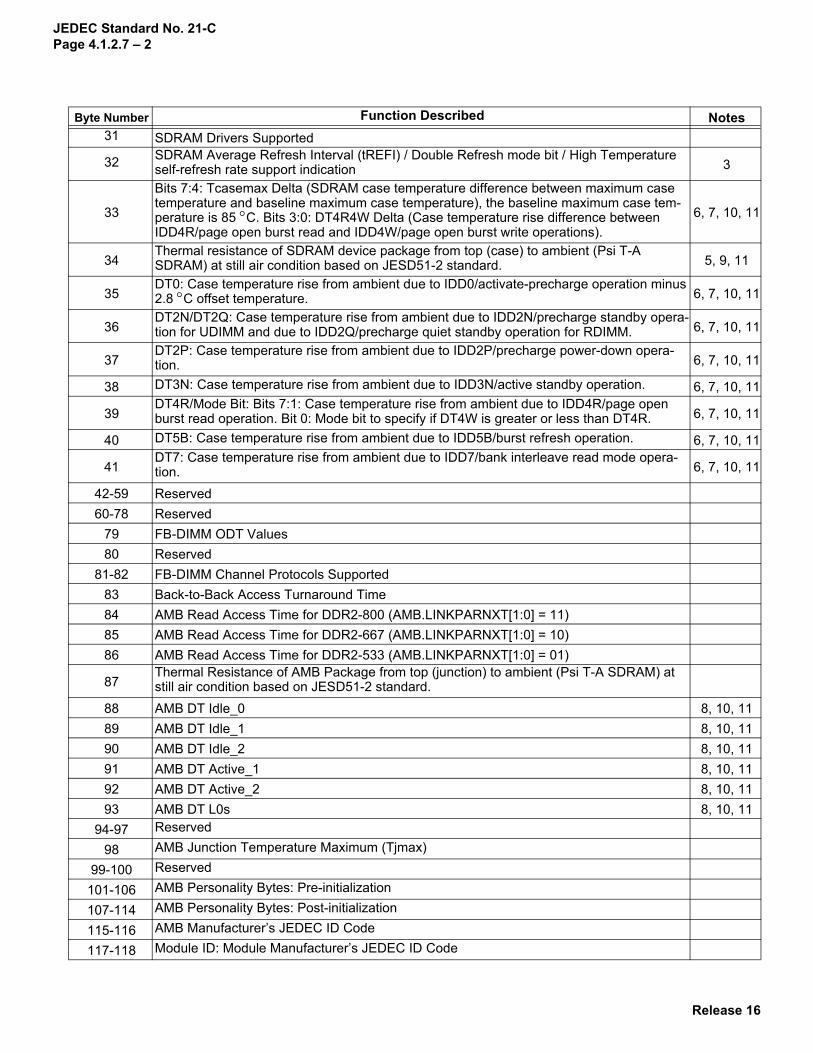
Byte Number Function Described Notes
0 Number of Serial PD Bytes Written / SPD Device Size / CRC Coverage 1,21 SPD Revision2 Key Byte / DRAM Device Type3 Voltage Levels of this Assembly4 SDRAM Addressing5 Module Physical Attributes6 Module Type / Thickness7 Module Organization8 Fine Timebase Dividend and Divisor9 Medium Timebase Dividend
10 Medium Timebase Divisor11 SDRAM Minimum Cycle Time (tCKmin) 312 SDRAM Maximum Cycle Time (tCKmax) 313 SDRAM CAS Latencies Supported14 SDRAM Minimum CAS Latency Time (tCAS)15 SDRAM Write Recovery Times Supported16 SDRAM Write Recovery Time (tWR) 317 SDRAM Write Latencies Supported18 SDRAM Additive Latencies Supported19 SDRAM Minimum RAS to CAS Delay (tRCD) 320 SDRAM Minimum Row Active to Row Active Delay (tRRD) 321 SDRAM Minimum Row Precharge Time (tRP) 322 SDRAM Upper Nibbles for tRAS and tRC 323 SDRAM Minimum Active to Precharge Time (tRAS) 324 SDRAM Minimum Auto-Refresh to Active/Auto-Refresh Time (tRC) 3
25-26 SDRAM Minimum Auto-Refresh to Active/Auto-Refresh Command Period (tRFC) 327 SDRAM Internal Write to Read Command Delay (tWTR) 328 SDRAM Internal Read to Precharge Command Delay (tRTP) 329 SDRAM Burst Lengths Supported30 SDRAM Terminations Supported
Appendix G: Serial Presence Detect (SPD) for Fully Buffered DIMM (Revision 1.1)
1.0 IntroductionThis appendix describes the serial presence detect (SPD) values for Fully Buffered DIMMs. These presence detects are those referenced in the SPD standard document for ‘Specific Features’. The following SPD fields will occur in the order presented in section 1.1. Note that the descriptions of Bytes 0 and 1 are different from those found in previous SPD standards. Further description of Byte 2 is found in Appendix A of the SPD standard. All unused entries wiil be coded as 0x00. All unused bits in defined bytes will be coded as 0 except where noted.
1.1 Address mapThe following is the SPD address map for FB-DIMM, i.e., when the value in Key Byte 2 is 0x09. It describes where the individual look-up table entries will be held in the serial EEPROM.
JEDEC Standard No. 21-CPage 4.1.2.7 – 2
Byte Number Function Described Notes31 SDRAM Drivers Supported
32 SDRAM Average Refresh Interval (tREFI) / Double Refresh mode bit / High Temperature self-refresh rate support indication 3
33
Bits 7:4: Tcasemax Delta (SDRAM case temperature difference between maximum case temperature and baseline maximum case temperature), the baseline maximum case tem-perature is 85 °C. Bits 3:0: DT4R4W Delta (Case temperature rise difference between IDD4R/page open burst read and IDD4W/page open burst write operations).
6, 7, 10, 11
34Thermal resistance of SDRAM device package from top (case) to ambient (Psi T-A SDRAM) at still air condition based on JESD51-2 standard. 5, 9, 11
35DT0: Case temperature rise from ambient due to IDD0/activate-precharge operation minus 2.8 °C offset temperature. 6, 7, 10, 11
36DT2N/DT2Q: Case temperature rise from ambient due to IDD2N/precharge standby opera-tion for UDIMM and due to IDD2Q/precharge quiet standby operation for RDIMM. 6, 7, 10, 11
37DT2P: Case temperature rise from ambient due to IDD2P/precharge power-down opera-tion. 6, 7, 10, 11
38 DT3N: Case temperature rise from ambient due to IDD3N/active standby operation. 6, 7, 10, 11
39DT4R/Mode Bit: Bits 7:1: Case temperature rise from ambient due to IDD4R/page open burst read operation. Bit 0: Mode bit to specify if DT4W is greater or less than DT4R. 6, 7, 10, 11
40 DT5B: Case temperature rise from ambient due to IDD5B/burst refresh operation. 6, 7, 10, 11
41DT7: Case temperature rise from ambient due to IDD7/bank interleave read mode opera-tion. 6, 7, 10, 11
42-59 Reserved60-78 Reserved
79 FB-DIMM ODT Values80 Reserved
81-82 FB-DIMM Channel Protocols Supported83 Back-to-Back Access Turnaround Time84 AMB Read Access Time for DDR2-800 (AMB.LINKPARNXT[1:0] = 11)85 AMB Read Access Time for DDR2-667 (AMB.LINKPARNXT[1:0] = 10)86 AMB Read Access Time for DDR2-533 (AMB.LINKPARNXT[1:0] = 01)
87Thermal Resistance of AMB Package from top (junction) to ambient (Psi T-A SDRAM) at still air condition based on JESD51-2 standard.
88 AMB DT Idle_0 8, 10, 1189 AMB DT Idle_1 8, 10, 1190 AMB DT Idle_2 8, 10, 1191 AMB DT Active_1 8, 10, 1192 AMB DT Active_2 8, 10, 1193 AMB DT L0s 8, 10, 11
94-97 Reserved
98 AMB Junction Temperature Maximum (Tjmax)
99-100 Reserved
101-106 AMB Personality Bytes: Pre-initialization
107-114 AMB Personality Bytes: Post-initialization
115-116 AMB Manufacturer’s JEDEC ID Code
117-118 Module ID: Module Manufacturer’s JEDEC ID Code
Release 16

R
JEDEC Standard No. 21-CPage 4.1.2.7– 3
119 Module ID: Module Manufacturing Location
120-121 Module ID: Module Manufacturing Date
122-125 Module ID: Module Serial Number
126-127 Cyclical Redundancy Code
128-145 Module Part Number 4
146-147 Module Revision Code 4
148-149 SDRAM Manufacturer’s JEDEC ID Code 4
150-175 Manufacturer’s Specific Data 4
176-255 Open for customer use
1. Number of SPD bytes written will typically be programmed as 128 or 176 bytes.2. Size of SPD device will typically be programmed as 256 bytes.3. From SDRAM datasheet.4. These are optional, in accordance with the JEDEC spec.5. Refer to JESD51-3 “Low Effective Thermal Conductivity Test Board for Leaded Surface Mount Packages” under
JESD51-2 standard.6. DT parameter is derived as following: DTx = IDDx * VDD * Psi T-A, where IDDx definition is based on JEDEC
DDR2 Component Specification and at VDD = 1.9 V, it is the datasheet (worst case) value, and Psi T-A is the pro-grammed value of Psi T-A (value in SPD Byte 33). Programmed temperature rise data (DTx) is based on the pro-grammed value of Psi T-A (value in SPD byte 33).
7. All DT parameters are defined for DDR2 SDRAM densities up to 2 Gbit. 4 Gbit parameters will be defined later.8. DT parameters for the AMB are derived as following: DTx = (IDDx * VDD * Psi T-A) + (ICCx * VCC * Psi T-A) +
(IDDSPDx * VDDSPD * Pxi T-A) where IDDx is at VDD = 1.9 V, ICCx is at VCC = 1.535 V, and IDDSPDx is at VDDSPD = 3.6 V; these are the active AMB powers corresponding to the AMB’s respective DIMM configuration loading. The IDDx, ICCx, and ISPDx are worst case values. Psi T-A used to program DTx is the programmed value of AMB Psi T-A (value in SPD byte 47).
9. Rule for rounding off thermal resistance values: Pxi X-X shall be rounded such that it is nearest/closest to the true value of Psi X-X.
10. Rule for rounding off DTx: DTx shall be rounded such that it is nearest/closest to the calculated value of DTx.11. Thermal bytes are for the DIMM as shipped, with any associated heat spreader, heat sink, mechanical clips, and
label.
Byte Number Function Described Notes
elease 16

Release 16
JEDEC Standard No. 21-CPage 4.1.2.7 – 4
2.0 Details of each byte
2.1 General Section: Bytes 0 to 59
This section contains fields which with little modification can be used for SPD definitions for non-FB-DIMM modules.
Byte 0: Number of Bytes Utilized / Number of Bytes in SPD Device / CRC Coverage
The least significant nibble of this byte describes the total number of bytes used by the module manufacturer for the SPD data and any (optional) specific supplier information. The byte count includes the fields for all required and optional data. Bits 6-4 describe the total size of the serial memory used to hold the Serial Pres-ence Detect data. Bit 7 indicates whether the unique module identifier (found in bytes 117 to 125) is covered by the CRC encoded on bytes 126 and 127.
Byte 1: SPD Revision
This byte describes the compatibility level of the encoding of the bytes contained in the SPD EEPROM, and the current collection of valid defined bytes. This byte must be coded as 0x11 for SPDs with revision level 1.1. Software should examine the upper nibble(Encoding Level) to determine if it can correctly interpret the con-tents of the module SPD. The lower nibble (Additions Level) can optionally be used to determine which addi-tional bytes or attribute bits have been defined; however, since any undefined additional byte must be encoded as 0x00 or undefined attribute bit must be defined as 0, software can safely detect additional bytes and use safe defaults if a zero encoding is read for these bytes.
Bit 7 Bit 6 ~ 4 Bit 3 ~ Bit 0
CRC Coverage SPD Bytes Total SPD Bytes Used
0 = CRC covers bytes 0 ~ 125 1 = CRC covers bytes 0 ~ 116
Bit [6, 5, 4] : 000 = Undefined 001 = 256 All Others TBD
Bit [3, 2, 1, 0] : 0000 = Undefined 0001 = 128 0010 = 176 0011 = 256 All Others TBD
SPD RevisionEncoding Level Additions Level
HexBit 7 Bit 6 Bit 5 Bit 4 Bit 3 Bit 2 Bit 1 Bit 0
Revision 0.0 0 0 0 0 0 0 0 0 00
Undefined 0 0 0 0 0 0 0 1 01
... . . . . . . . . .
Revision 1.0 0 0 0 1 0 0 0 0 10
Revision 1.1 0 0 0 1 0 0 0 1 11
... . . . . . . . . ...
Undefined 1 1 1 1 1 1 1 1 FF

Relea
JEDEC Standard No. 21-CPage 4.1.2.7– 5
Byte 2: Key ByteThis byte is the key byte used by BIOS to determine how to interpret all other bytes in the SPD EEPROM. BIOS must check this byte first to ensure that the EEPROM data is interpreted correctly. Any SDRAM or Module type that requires significant changes to the SPD format (beyond defining previously undefined bytes or bits) also requires a new entry in the key byte table below.
Byte 3: Voltage Levels of this AssemblyThis byte describes the expected voltage level for two power supplies that are connected to the module. For example, Fully Buffered DIMM Power Supply 1 is defined as the supply for the channel interface, and Power Supply 2 is defined as the supply for the DRAM interface.
Line # SDRAM / Module Type Corresponding to Key Byte Bit 7 Bit 6 Bit 5 Bit 4 Bit 3 Bit 2 Bit 1 Bit 0 Hex
0 Reserved 0 0 0 0 0 0 0 0 00
1 Standard FPM DRAM 0 0 0 0 0 0 0 1 01
2 EDO 0 0 0 0 0 0 1 0 02
3 Pipelined Nibble 0 0 0 0 0 0 1 1 03
4 SDRAM 0 0 0 0 0 1 0 0 04
5 ROM 0 0 0 0 0 1 0 1 05
6 DDR1 SGRAM 0 0 0 0 0 1 1 0 06
7 DDR1 SDRAM 0 0 0 0 0 1 1 1 07
8 DDR2 SDRAM 0 0 0 0 1 0 0 0 08
9 DDR2 SDRAM FB-DIMM 0 0 0 0 1 0 0 1 09
10 DDR2 SDRAM FB-DIMM PROBE 0 0 0 0 1 0 1 0 0A
- - - - - - - - - - -
253 TBD 1 1 1 1 1 1 0 1 FD
254 TBD 1 1 1 1 1 1 1 0 FE
255 TBD 1 1 1 1 1 1 1 1 FF
Bit 7 ~ 4 Bit 3 ~ Bit 0
Power Supply 2 Power Supply 1
Bit [7, 6, 5, 4] : 0000 = Undefined 0001 = 1.8 V 0010 = 1.5 V 0011 = 1.2 V All Others TBD
Bit [3, 2, 1, 0] : 0000 = Undefined 0001 = 1.8 V 0010 = 1.5 V 0011 = 1.2 V All Others TBD
se 16

JEDEC Standard No. 21-CPage 4.1.2.7 – 6
Byte 4: SDRAM AddressingThis byte describes the row addressing, the column addressing, and the number of banks in the SDRAM device. Bits 1-0 encode the number of banks, bits 4-2 encode the number of column address bits, and bits 7-5 encode the number of row address bits.
Byte 5: Module Physical Attributes This byte describes the height and thickness of the SDRAM module. Bits 2-0 encode the module thickness, which is defined as the maximum value including all finished assembly parts: devices, heat spreaders, or other mechanical components. Encodings for bits 2-0 will depend on the value of Byte 6, the Module Type.
Decoding of the Module Thickness field, based on Module Type (units in mm) is shown below. Table entries other than FB-DIMM are shown for reference only.
Bit 7 ~ 5 Bit 4 ~ 2 Bit 1 ~ Bit 0
Row Address Bits Column Address Bits Number of Banks
Bit [7, 6, 5] : 000 = 12 001 = 13 010 = 14 011 = 15 All Others TBD
Bit [4, 3, 2] : 0000 = 9 0001 = 10 0010 = 11 All Others TBD
Bit [1, 0] : 00 = 4 01 = 8 10 = 16 11 = 32
Bit 7 ~ Bit 6 Bit 5 ~ Bit 3 Bit 2 ~ Bit 0
Reserved Module Height(mm)
Module Thickness(mm)
Bit [5, 4, 3] : 000 = Undefined 001 = 15 < x ≤ 20 010 = 20 < x ≤ 25 011 = 25 < x ≤ 30 100 = 30 < x ≤ 35 101 = 35 < x ≤ 40 All others undefined
Bit [2, 1, 0] : See indexed tables below
Module Thickness FB-DIMM RDIMM UDIMM SO-DIMM Micro-
DIMM Mini-RDIMM Mini-UDIMM
Bit 2 Bit 1 Bit 0 Byte 6 [3:0]= 0111
Byte 6 [3:0]= 0001
Byte 6 [3:0]= 0010
Byte 6 [3:0]= 0011
Byte 6 [3:0]= 0100
Byte 6 [3:0]= 0101
Byte 6 [3:0]= 0110
0 0 0 Undefined / Not specified
0 0 1 x ≤ 6.0 x ≤ 4.10 x ≤ 4.10 x ≤ 3.80 x ≤ 3.80 x ≤ 3.85 x ≤ 3.85
0 1 0 6.0 < x ≤ 7.0 4.10 < x ≤ 6.75 4.10 < x ≤ 6.75 Reserved Reserved 3.85 < x ≤ 6.45 3.85 < x ≤ 6.45
0 1 1 7.0 < x ≤ 8.0 6.75 < x ≤ 7.55 6.75 < x ≤ 7.55 Reserved Reserved 6.45 < x ≤ 7.25 6.45 < x ≤ 7.25
1 0 0 8.0 < x ≤ 9.0 7.55 < x 7.55 < x Reserved Reserved 7.25 < x 7.25 < x
1 0 1 9.0 < x Reserved Reserved Reserved Reserved Reserved Reserved
1 1 0 Reserved Reserved Reserved Reserved Reserved Reserved Reserved1 1 1 Reserved Reserved Reserved Reserved Reserved Reserved Reserved
Release 16

Relea
JEDEC Standard No. 21-CPage 4.1.2.7– 7
Byte 6: Module Type
This byte identifies the SDRAM memory module type and also indicates the width of the module. BIOS uses the module type information in this byte to determine the encoding of the module thickness field in byte 5. Table entries other than FB-DIMM are shown for reference only.
Byte 7: Module OrganizationThis byte describes the organization of the SDRAM module. Bits 2-0 encode the device width of the SDRAM devices. Bits 5-3 encode the number of physical ranks on the SDRAM. For example, for a single-rank module with x8 SDRAMs, this byte is encoded 00 001 001, or 0x09.
Bit 7 ~ Bit 4 Bit 3 ~ Bit 0
Reserved Module Type
Bit [3, 2, 1, 0] : 0000 = Undefined 0001 = RDIMM (width = 133.35 mm nom) 0010 = UDIMM (width = 133.35 mm nom) 0011 = SO-DIMM (width = 67.6 mm nom) 0100 = Micro-DIMM (width = 54.0 mm nom) 0101 = Mini-RDIMM (width = 82.0 mm nom) 0110 = Mini-UDIMM (width = 82.0 mm nom) 0111 = FB-DIMM (width = 133.35 mm nom) All others TBD
Definitions: RDIMM: Registered Dual In-Line Memory Module UDIMM: Unbuffered Dual In-Line Memory Module SO-DIMM: Small Outline Dual In-Line Memory Module Micro-DIMM: Micro Dual In-Line Memory Module Mini-RDIMM: Mini Registered Dual In-Line Memory Module Mini-UDIMM: Mini Unbuffered Dual In-Line Memory Module FB-DIMM: Fully Buffered Dual In-Line Memory Module
Bit 7 ~ Bit 6 Bit 5 ~ Bit 3 Bit 2 ~ Bit 0
Reserved Number of Ranks SDRAM Device Width
Bit [5, 4, 3] : 000 = Undefined 001 = 1 Rank 010 = 2 Ranks All others undefined
Bit [2, 1, 0] : 000 = 4 bits 001 = 8 bits 010 = 16 bits 011 = 32 bits All others undefined
se 16

JEDEC Standard No. 21-CPage 4.1.2.7 – 8
Byte 8: Fine Timebase (FTB) Dividend / Divisor
This byte defines a value in picoseconds that represents the fundamental timebase for fine grain timing calcu-lations. This value is used as a multiplier for formulating subsequent timing parameters. The fine timebase (FTB) is defined as the fine timebase dividend, bits 7~4, divided by the fine timebase divisor, bits 3~0. A value of 0x00 should only be programmed if the FTB is not utilized by any SPD fields.
Examples:
Byte 9: Medium Timebase (MTB) DividendByte 10: Medium Timebase (MTB) Divisor
These bytes define a value in nanoseconds that represents the fundamental timebase for medium grain tim-ing calculations. This value is typically the greatest common divisor for the range of clock frequencies (clock periods) supported by a particular SDRAM. This value is used as a multiplier for formulating subsequent tim-ing parameters. The medium timebase (MTB) is defined as the medium timebase dividend (byte 9) divided by the medium timebase divisor (byte 10).
Examples:
To simplify BIOS implementation, DIMMs associated with a given key byte value may differ in MTB value only by a factor of two. For DDR2 FB-DIMM (key byte values 0x09 and 0x10), the defined MTB values are:
Bit 7 ~ Bit 4 Bit 3 ~ Bit 0
Fine Timebase (FTB) Dividend Fine Timebase (FTB) Divisor
Values defined from 0 to 15 Values defined from 0 to 15
Dividend Divisor Timebase (ps) Use
5 1 5 When time granularity of 5 ps is required5 2 2.5 When time granularity of 2.5 ps is required
Byte 9 Bit 7 ~ Bit 0 Byte 10 Bit 7 ~ Bit 0
Medium Timebase (MTB) Dividend Medium Timebase (MTB) Divisor
Values defined from 1 to 255 Values defined from 1 to 255
Dividend Divisor Timebase (ns) Use
1 4 0.25 For clock frequencies of 200, 267, 333, and 400 MHz1 8 0.125 For clock frequencies of 400, 533, 667, and 800 MHz
Dividend Divisor Timebase (ns) Use
1 4 0.25 FB-DIMM MTB Value1 8 0.125 FB-DIMM MTB Value
Release 16

Relea
JEDEC Standard No. 21-CPage 4.1.2.7– 9
Byte 11: Minimum SDRAM Cycle Time (tCKmin)
This byte defines the minimum cycle time for the SDRAM module, in medium timebase (MTB) units. This number applies to all applicable components on the module. This byte applies to SDRAM and support com-ponents as well as the overall capability of the DIMM.
Examples:
Byte 12: Maximum SDRAM Cycle Time (tCKmax)
This byte defines the maximum cycle time for the SDRAM module, in medium timebase (MTB) units. This number applies to all applicable components on the module. This byte applies to SDRAM and support com-ponents as well as the overall capability of the DIMM.
Examples:
Bit 7 ~ Bit 0
Mimimum SDRAM Cycle Time (tCKmin)MTB Units
Values defined from 1 to 255
tCKmin(MTB units)
Timebase(ns)
tCKmin Result(ns)
Use
20 0.25 5 DDR2 with 200 MHz clock15 0.25 3.75 DDR2 with 266 MHz clock12 0.25 3 DDR2 with 333 MHz clock10 0.25 2.5 DDR2 with 400 MHz clock20 0.125 2.5 DDR3 with 400 MHz clock15 0.125 1.875 DDR3 with 533 MHz clock12 0.125 1.5 DDR3 with 667 MHz clock10 0.125 1.25 DDR3 with 800 MHz clock
Bit 7 ~ Bit 0
Maximum SDRAM Cycle Time (tCKmax)MTB Units
Values defined from 1 to 255
tCKmax(MTB units)
Timebase(ns)
tCKmax Result(ns)
Use
32 0.25 8 DDR2, 125 MHz maximum clock period64 0.125 8 DDR3, 125 MHz maximum clock period
se 16

JEDEC Standard No. 21-CPage 4.1.2.7 – 10
Byte 13: CAS Latencies Supported
This field describes the CAS Latency (CL) values supported by the SDRAMs on the memory module, in units of memory clocks. The lower four bits describe the lowest value of CL, and the upper four bits describe the range, defined as total number of values supported. For example, SDRAMs that support CAS latencies 3, 4, and 5 would program a CL Range of 3 and a minimum CL of 3: 0011 0011 = 0x33.
Bit 7 ~ Bit 4 Bit 3 ~ Bit 0
CL Range (clocks) Minimum CL (clocks)
Bit [7, 6, 5, 4] : 0000 = Undefined 0001 = 1 0010 = 2 0011 = 3 0100 = 4 All other values TBD
Bit [3, 2, 1, 0] : 0011 = 3 0100 = 4 0101 = 5 0110 = 6 All other values TBD
Release 16
Relea
JEDEC Standard No. 21-CPage 4.1.2.7– 11
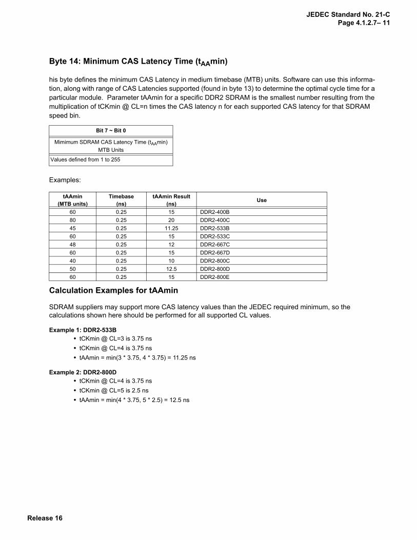
Byte 14: Minimum CAS Latency Time (tAAmin)
his byte defines the minimum CAS Latency in medium timebase (MTB) units. Software can use this informa-tion, along with range of CAS Latencies supported (found in byte 13) to determine the optimal cycle time for a particular module. Parameter tAAmin for a specific DDR2 SDRAM is the smallest number resulting from the multiplication of tCKmin @ CL=n times the CAS latency n for each supported CAS latency for that SDRAM speed bin.
Examples:
Calculation Examples for tAAmin
SDRAM suppliers may support more CAS latency values than the JEDEC required minimum, so the calculations shown here should be performed for all supported CL values.
Example 1: DDR2-533B• tCKmin @ CL=3 is 3.75 ns• tCKmin @ CL=4 is 3.75 ns• tAAmin = min(3 * 3.75, 4 * 3.75) = 11.25 ns
Example 2: DDR2-800D• tCKmin @ CL=4 is 3.75 ns• tCKmin @ CL=5 is 2.5 ns• tAAmin = min(4 * 3.75, 5 * 2.5) = 12.5 ns
Bit 7 ~ Bit 0
Mimimum SDRAM CAS Latency Time (tAAmin)MTB Units
Values defined from 1 to 255
tAAmin(MTB units)
Timebase(ns)
tAAmin Result(ns) Use
60 0.25 15 DDR2-400B80 0.25 20 DDR2-400C45 0.25 11.25 DDR2-533B60 0.25 15 DDR2-533C48 0.25 12 DDR2-667C60 0.25 15 DDR2-667D40 0.25 10 DDR2-800C50 0.25 12.5 DDR2-800D60 0.25 15 DDR2-800E
se 16

JEDEC Standard No. 21-CPage 4.1.2.7 – 12
CAS Latency Calculation and Examples
CAS latency is not a purely analog value as DDR2 SDRAMs use the DLL to synchronize data and strobe outputs with the clock. All possible frequencies may not be tested, therefore an application should use the next smaller JEDEC standard tCKmin value (5.0, 3.75, 3.0, or 2.5 ns) when calculating CAS Latency. This section shows how the BIOS calculates CAS latency based on Bytes 11 ~ 14.
Step 1: The BIOS first determines the common operating frequency of all modules in the system, ensuring that the corresponding value of tCK (tCKactual) falls between tCKmin (Byte 11) and tCKmax (Byte 12). If tCKactual is not a JEDEC standard value, the next smaller standard tCKmin value is used for calculating CAS Latency.
Step 2: The BIOS then calculates the “desired” CAS Latency (CLdesired):CLdesired = ceiling ( tAAmin / tCKactual )
where tAAmin is defined in Byte 14. The ceiling function requires that the quotient be rounded up always.
Step 3: The BIOS then determines the “actual” CAS Latency (CLactual):CLactual = max ( CLdesired, min CL supported)
where min CL supported is found the in the least significant nibble of Byte 13.
Example 1: DDR2-533C 4-4-4 module operating at 533tAAmin = 15 nsMin CL = 3, range = 3 (CL = 3, 4, 5 supported)tCK actual = 3.75 ns (266 MHz Clock)CLdesired = ceiling (15 / 3.75) = 4CLactual = max (4, 3) = 4
Example 2: DDR2-667C 4-4-4 standard latency module operating at 533tAAmin = 12 nsMin CL = 4, range = 3 (CL = 4, 5, 6 supported)tCK actual = 3.75 ns (266 MHz Clock)CLdesired = ceiling (12 / 3.75) = 4CLactual = max (4, 4) = 4
Example 3: DDR2-667 4-4-4 fast latency module operating at 533 (downshifting to 3-3-3)tAAmin = 11.25 ns (chosen to allow CL=3 at 533, exceeds value required to meet minimum JEDEC standard)Min CL = 3, range = 3 (CL = 3, 4, 5 supported)tCK actual = 3.75 ns (266 MHz Clock)CLdesired = ceiling (11.25 / 3.75) = 3CLactual = max (3, 3) = 3
Example 4: DDR2-800D 5-5-5 module operating at 313 (debug & hardware bringup scenario)tAAmin = 12.5 nsMin CL = 4, range = 3 (CL = 4, 5, 6 supported)tCK actual = 3.2 ns (156 MHz Clock) reduced to next lower JEDEC standard tCKmin = 3.0 nsCLdesired = ceiling (12.5 / 3.0) = 5CLactual = max (5, 4) = 5
Release 16

Relea
JEDEC Standard No. 21-CPage 4.1.2.7– 13
Byte 15: Write Recovery Times Supported
This field describes the Write Recovery (WR) values supported by the SDRAMs on the memory module, in units of memory clocks. The lower four bits describe the lowest value of WR, and the upper four bits describe the range, defined as total number of values supported. For example, SDRAMs that support WR values of 2 and 3 would program a WR Range of 2 and a minimum WR of 2: 0010 0010 = 0x22.
Byte 16: Write Recovery Time (tWR)
This byte defines the SDRAM write recovery time in medium timebase (MTB) units.
Example:
Bit 7 ~ Bit 4 Bit 3 ~ Bit 0
WR Range (clocks) Minimum WR (clocks)
Bit [7, 6, 5, 4] : 0000 = Undefined 0001 = 1 0010 = 2 0011 = 3 0100 = 4 0101 = 5 All other values TBD
Bit [3, 2, 1, 0] : 0010 = 2 All other values TBD
Bit 7 ~ Bit 0
Mimimum Write Recovery Time (tWR)MTB Units
Values defined from 1 to 255
tWR(MTB units)
Timebase(ns)
tWR Result(ns) Use
60 0.25 15 All DDR2 speed grades
se 16

JEDEC Standard No. 21-CPage 4.1.2.7 – 14
Byte 17: Write Latencies Supported
This field describes the Write Latency (WL) values supported by the SDRAMs on the memory module, in units of memory clocks. The lower four bits describe the lowest value of WL, and the upper four bits describe the range, defined as total number of values supported. For example, SDRAMs that support WL values of 2, 3, and 4 would program a WL Range of 3 and a minimum WL of 2: 0011 0010 = 0x32.
Byte 18: Additive Latencies Supported
This field describes the Additive Latency (AL) values supported by the SDRAMs on the memory module, in units of memory clocks. The lower four bits describe the lowest value of AL, and the upper four bits describe the range, defined as total number of values supported. For example, SDRAMs that support AL values of 0, 1, 2, and 3 would program a AL Range of 4 and a minimum AL of 0: 0100 0000 = 0x40.
Bit 7 ~ Bit 4 Bit 3 ~ Bit 0
WL Range (clocks) Minimum WL (clocks)
Bit [7, 6, 5, 4] : 0000 = Undefined 0001 = 1 0010 = 2 0011 = 3 0100 = 4 0101 = 5 0110 = 6 0111 = 7 1000 = 8 1001 = 9 All other values TBD
Bit [3, 2, 1, 0] : 0010 = 2 All other values TBD
Bit 7 ~ Bit 4 Bit 3 ~ Bit 0
AL Range (clocks) Minimum AL (clocks)
Bit [7, 6, 5, 4] : 0000 = Undefined 0001 = 1 0010 = 2 0011 = 3 0100 = 4 0101 = 5 0110 = 6 All other values TBD
Bit [3, 2, 1, 0] : 0000 = 0 All other values TBD
Release 16

Relea
JEDEC Standard No. 21-CPage 4.1.2.7– 15
Byte 19: Minimum RAS to CAS Delay (tRCD)
This byte defines the SDRAM RAS# to CAS# Delay in medium timebase (MTB) units.
Examples:
Byte 20: Minimum Row Active to Row Active Delay (tRRD)
This byte defines the minimum SDRAM Row Active to Row Active Delay in medium timebase units.
Examples:
Bit 7 ~ Bit 0
Minimum RAS# to CAS# Delay (tRCD)MTB Units
Values defined from 1 to 255
tRCD(MTB units)
Timebase(ns)
tRCD Result (ns) Use
60 0.25 15 3 clocks at DDR2-400B80 0.25 20 4 clocks at DDR2-400C45 0.25 11.25 3 clocks at DDR2-533B60 0.25 15 4 clocks at DDR2-533C48 0.25 12 4 clocks at DDR2-667C60 0.25 15 5 clocks at DDR2-667D40 0.25 10 4 clocks at DDR2-800C50 0.25 12.5 5 clocks at DDR2-800D60 0.25 15 6 clocks at DDR2-800E
Bit 7 ~ Bit 0
Minimum Row Active to Row Active Delay (tRRD)MTB Units
Values defined from 1 to 255
tRRD(MTB units)
Timebase(ns)
tRRD Result(ns) Use
30 0.25 7.5 For SDRAMs with 1KB page size40 0.25 10 For SDRAMs with 2KB page size
se 16

JEDEC Standard No. 21-CPage 4.1.2.7 – 16
Byte 21: Minimum Row Precharge Time (tRP)
This byte defines the SDRAM minimum Row Precharge Time Delay in medium timebase (MTB) units.
Examples:
Byte 22: Upper Nibbles for tRAS and tRC
This byte defines the most significant nibbles for the values of tRAS (byte 23) and tRC (byte 24).
Bit 7 ~ Bit 0
Minimum Row Precharge Time (tRP)MTB Units
Values defined from 1 to 255
tRP(MTB units)
Timebase(ns)
tRP Result (ns) Use
60 0.25 15 3 clocks at DDR2-400B80 0.25 20 4 clocks at DDR2-400C45 0.25 11.25 3 clocks at DDR2-533B60 0.25 15 4 clocks at DDR2-533C48 0.25 12 4 clocks at DDR2-667C60 0.25 15 5 clocks at DDR2-667D40 0.25 10 4 clocks at DDR2-800C50 0.25 12.5 5 clocks at DDR2-800D60 0.25 15 6 clocks at DDR2-800E
Bit 7 ~ Bit 4 Bit 3 ~ Bit 0
tRC Most Significant Nibble tRAS Most Significant Nibble
See Byte 24 description See Byte 23 description
Release 16

Relea
JEDEC Standard No. 21-CPage 4.1.2.7– 17
Byte 23: Minimum Active to Precharge Time (tRAS)
The lower nibble of Byte 22 and the contents of Byte 23 combined create a 12-bit value which defines the SDRAM minimum Active to Precharge Time Delay in medium timebase (MTB) units. The most significant bit is Bit 3 of Byte 22, and the least significant bit is Bit 0 of Byte 23.
Examples:
Byte 24: Minimum Active to Active/Refresh Time (tRC)
The upper nibble of Byte 22 and the contents of Byte 24 combined create a 12-bit value which defines the SDRAM minimum Active to Active/Refresh Time Delay in medium timebase (MTB) units. The most signifi-cant bit is Bit 7 of Byte 22, and the least significant bit is Bit 0 of Byte 24.
Examples:
Byte 22 Bit 3 ~ Bit 0, Byte 23 Bit 7 ~ Bit 0
Minimum Active to Precharge Time (tRAS)MTB Units
Values defined from 1 to 4095
tRAS(MTB units)
Timebase(ns)
tRAS Result (ns) Use
180 0.25 45 9 clocks at DDR2-400C12 clocks at DDR2-53315 clocks at DDR2-66718 clocks at DDR2-800
160 0.25 40 8 clocks at DDR2-400B320 0.125 40 16 clocks at DDR3-800 (e.g.)
Byet 22 Bit 7 ~ Bit 4, Byte 24 Bit 7 ~ Bit 0
Minimum Active to Active/Refresh Time (tRC)MTB Units
Values defined from 1 to 4095
tRC(MTB units)
Timebase(ns)
tRC Result (ns) Use
260 0.25 65 13 clocks at DDR2-400C220 0.25 55 11 clocks at DDR2-400B240 0.25 60 16 clocks at DDR2-533C225 0.25 56.25 15 clocks at DDR2-533B240 0.25 60 20 clocks at DDR2-667D228 0.25 57 19 clocks at DDR2-667C220 0.25 55 22 clocks at DDR2-800E210 0.25 52.5 21 clocks at DDR2-800D200 0.25 50 20 clocks at DDR2-800C
se 16

JEDEC Standard No. 21-CPage 4.1.2.7 – 18
Byte 25: Minimum Refresh Recovery Time Delay (tRFC), Least Significant BitsByte 26: Minimum Refresh Recovery Time Delay (tRFC), Most Significant Bits
The contents of Byte 25 and the contents of Byte 26 combined create a 16-bit value which defines the SDRAM minimum Refresh Recovery Time Delay in medium timebase (MTB) units. The most significant bit is Bit 7 of Byte 26, and the least significant bit is Bit 0 of Byte 25.
Examples:
Byte 26 Bit 7 ~ Bit 0, Byte 26 Bit 7 ~ Bit 0
Minimum Refresh Recover Time Delay (tRFC)MTB Units
Values defined from 1 to 65535
tRFC(MTB units)
Timebase(ns)
tRFC Result (ns) Use
300 0.25 75 15 clocks at DDR2-40020 clocks at DDR2-53325 clocks at DDR2-66730 clocks at DDR2-800
420 0.25 105 21 clocks at DDR2-40028 clocks at DDR2-53335 clocks at DDR2-66742 clocks at DDR2-800
510 0.25 127.5 25.5 clocks at DDR2-400 *34 clocks at DDR2-53342.5 clocks at DDR2-667 *51 clocks at DDR2-800
780 0.25 195 39 clocks at DDR2-40052 clocks at DDR2-53365 clocks at DDR2-66778 clocks at DDR2-800
1310 0.25 327.5 65.5 clocks at DDR2-400 *87.3 clocks at DDR2-533 *109.2 clocks at DDR2-667 *131 clocks at DDR2-800
* Systems must round to the next higher integer value when calculating the number of clocks.
Release 16

Relea
JEDEC Standard No. 21-CPage 4.1.2.7– 19
Byte 27: Minimum Internal Write to Read Command Delay (tWTR)
This byte defines the SDRAM internal write to read time in medium timebase (MTB) units.
Examples:
Byte 28: Minimum Internal Read to Precharge Command Delay (tRTP)
TThis byte defines the SDRAM internal Read to Precharge delay time in medium timebase (MTB) units.
Examples:
Bit 7 ~ Bit 0
Internal Write to Read Delay Time (tWTR)MTB Units
Values defined from 1 to 255
tWTR(MTB units)
Timebase(ns)
tWTR Result(ns) Use
40 0.25 10 DDR2-40030 0.25 7.5 DDR2-533, DDR2-667, DDR2-800
Bit 7 ~ Bit 0
Internal Read to Precharge Delay Time (tRTP)MTB Units
Values defined from 1 to 255
tRTP(MTB units)
Timebase(ns)
tRTP Result(ns) Use
30 0.25 7.5 All DDR2 speed bins
se 16

JEDEC Standard No. 21-CPage 4.1.2.7 – 20
Byte 29: Burst Lengths SupportedThis byte defines the read burst lengths supported by the SDRAM on this module.
Byte 30: Terminations SupportedThis byte defines the on-die termination values supported by the SDRAM on this module.
Byte 31: Drivers SupportedThis byte defines the optional drive strengths supported by the SDRAM on this module.
Bit 7 Bit 6 ~ 2 Bit 1 Bit 0
Burst Chop TBD BL = 8 BL = 4
0 = Not Supported1 = Supported
0 = Not Supported1 = Supported
0 = Not Supported1 = Supported
Bit 7 ~ Bit 3 Bit 2 Bit 1 Bit 0
TBD 50 Ω ODT 75 Ω ODT 150 Ω ODT
0 = Not Supported1 = Supported
0 = Not Supported1 = Supported
0 = Not Supported1 = Supported
Bit 7 ~ Bit 1 Bit 0
TBD Weak Driver
0 = Not Supported1 = Supported
Release 16

Relea
JEDEC Standard No. 21-CPage 4.1.2.7– 21
Byte 32: Average SDRAM Refresh Interval (tREFI)This byte describes the module’s average refresh rate over the standard operating temperature range.
Bit 7 defines whether or not double refresh is required for SDRAM case temperature exceeding 85 °C.
Bit 6 indicates DDR2 SDRAM “High Temperature Self-Refresh” support.
Bit 7 Bit 6 Bit 5 ~ Bit 4 Bit 3 ~ Bit 0
Double Refresh Requirement High TemperatureSelf-Refresh TBD
Average Refresh Interval (tREFI)μS
See bit description below See bit description below Bit [3, 2, 1, 0] : 0000 = 15.625 (normal) 0001 = 3.9 (reduced 0.25x) 0010 = 7.8 (reduced 0.5x) 0011 = 31.3 (extended 2x) 0100 = 62.5 (extended 4x) 0101 = 125 (extended 8x) All other values TBD
Bit 7 Byte 32, Bit 7
0 Do not need double refresh rate for the proper operation at the SDRAM maximum case temperature above 85 °C. The SDRAM maximum case temperature is specified at Byte 33.
1 Requires double refresh rate for the proper operation at the SDRAM maximum case temperature above 85 °C. The SDRAM maximum case temperature is specified at Byte 33.
Bit 6 Byte 32, Bit 6
0 SDRAM does not support high temperature self-refresh entry. Controller must ensure SDRAM cool down to Tcase < 85 °C before entering self-refresh
1SDRAM high temperature self-refresh entry supported. When needed, controller may set SDRAM in high temperature self-
refresh mode via EMRS(2) [A7] and be able to enter self-refresh above 85 °C Tcase temperature
se 16

Release 16
JEDEC Standard No. 21-CPage 4.1.2.7 – 22
Byte 33: Tcasemax
This byte is split into two nibbles. The higher order nibble (bits 4:7) describes the SDRAM case temperature difference between maximum case temperature and the baseline maximum case temperature of 85 °C. Unit for this field is 2 °C. The SDRAM maximum case temperature is 85 °C plus the value in bits 4:7. If bits 4:7 is zero, the SDRAM device only supports up to 85 °C maximum case temperature and users must ensure the case temperature will not exceed 85 °C in any operation. If bits 4:7 is non-zero, the maximum case temperature range is extended and users must look at byte 32 bit 7 for the proper operation at this extended case temperature.
The lower order nibble (bits 0:3) describes DT4R4W Delta ( the SDRAM case temperature rise difference from ambient due to IDD4R/page open burst read vs. IDD4W/page open burst write operations) at VDD = 1.9 V, in unit of 0.4 °C. Please refer to JEDEC DDR2 SDRAM Component Specification for the definitions of IDD4R and IDD4W operations. Please refer to Notes 5 & 6 of the”1.1 Address Map table” of this spec for calculation of temperature rise.
Byte 33: Tcasemax, Subfield A: 2 °C (Bits 7:4)Line # Tcasemax ( Unit: 2 0C ) Bit 7 Bit 6 Bit 5 Bit 4 Bit 3 Bit 2 Bit 1 Bit 0 Hex
0A 0 0 0 0 0 0-1A 2 0 0 0 1 1-2A 4 0 0 1 0 2-3A 6 0 0 1 1
See Subfield B3-
4A 8 0 1 0 0 4-5A 10 0 1 0 1 5-6A 12 0 1 1 0 6-7A 14 0 1 1 1 7-8A 16 1 0 0 0 8-9A 18 1 0 0 1 9-
10A 20 1 0 1 0See Subfield B
A-. . . . . . .. . . . . . .
14A 28 1 1 1 0 E-15A Exceed 30 1 1 1 1 F-
Byte 33: DT4R4W Delta, Subfield B: 0.4 °C (Bits 0:3)Line # DT4R4W Delta (Granularity: 0.4 0C ) Bit 7 Bit 6 Bit 5 Bit 4 Bit 3 Bit 2 Bit 1 Bit 0 Hex
0A Not Supported 0 0 0 0 -01A 0.4 0 0 0 1 -12A 0.8 0 0 1 0 -23A 1.2 0 0 1 1 -34A 1.6 0 1 0 0 -45A 2.0 0 1 0 1 -56A 2.4 0 1 1 0 -67A 2.8 0 1 1 1 -78A 3.2
See Subfield A1 0 0 0 -8
9A 3.6 1 0 0 1 -910A 4.0 1 0 1 0 -A
. . . . . . .
. . . . . . .14A 5.6 1 1 1 0 -E15A Exceed 6.0 1 1 1 1 -F

Release 16
JEDEC Standard No. 21-CPage 4.1.2.7– 23
Byte 34: Thermal Resistance of SDRAM Package from Top (Case) to Ambient( Psi T-A SDRAM )
This byte describes the thermal resistance of SDRAM package from top (case) to ambient and it is based on JESD51-3 “Low Effective Thermal Conductivity Test Board for Leaded Surface Mount Packages” under JESD51-2 standard. Unit for this field is 0.5 oC/W.
Byte 34: Thermal Resistance of SDRAM Package from Top (Case) to Ambient ( Psi T-A SDRAM )
Psi T-A SDRAM (Granularity: 0.5 0C/W ) Bit 7 Bit 6 Bit 5 Bit 4 Bit 3 Bit 2 Bit 1 Bit 0 HexNot Defined 0 0 0 0 0 0 0 0 00
0.5 0 0 0 0 0 0 0 1 011.0 0 0 0 0 0 0 1 0 021.5 0 0 0 0 0 0 1 1 032.0 0 0 0 0 0 1 0 0 04
. . . . . . . . . .
. . . . . . . . . .16.0 0 0 1 0 0 0 0 0 20
. . . . . . . . . .
. . . . . . . . . .30.0 0 0 1 1 1 1 0 0 3C
. . . . . . . . . .
. . . . . . . . . .127 1 1 1 1 1 1 1 0 FE
Exceed 127.5 1 1 1 1 1 1 1 1 FF

Release 16
JEDEC Standard No. 21-CPage 4.1.2.7 – 24
Byte 35: SDRAM Case Temperature Rise from Ambient due to Activate-Precharge (DT0)
In this byte, bits 7:2 describe DT0 ( SDRAM case temperature rise from ambient due to IDD0/activate-pre-charge operation minus 2.8 °C offset temperature ), in units of 0.3 °C. This value plus 2.8 °C is the SDRAM case temperature rise from ambient. Please refer to JEDEC DDR2 SDRAM Component Specification for the definition of IDD0 operation. Please refer to Notes 5 & 6 of the “1.1 Address Map table” of this spec for calcu-lation of temperature rise. Bits 1:0 are reserved for future use in describing SDRAM thermal characteristics.
Byte 35: DT0
Line # DT0 ( Granularity: 0.3 0C ) Bit 7 Bit 6 Bit 5 Bit 4 Bit 3 Bit 2 Bit 1 ~ Bit 0
0 Not Defined 0 0 0 0 0 0
1 0.3 0 0 0 0 0 1
2 0.6 0 0 0 0 1 0
3 0.9 0 0 0 0 1 1
4 1.2 0 0 0 1 0 0
5 1.5 0 0 0 1 0 1
6 1.8 0 0 0 1 1 0 Reserved
7 2.1 0 0 0 1 1 1
8 2.4 0 0 1 0 0 0
9 2.7 0 0 1 0 0 1
10 3.0 0 0 1 0 1 0
. . . . . . . .
. . . . . . . .
254 18.6 1 1 1 1 1 1
255 Exceed 18.6 1 1 1 1 1 1

Release 16
JEDEC Standard No. 21-CPage 4.1.2.7– 25
Byte 36: SDRAM Case Temperature Rise from Ambient due to Precharge/Quiet Standby (DT2N/DT2Q)For Unbuffered DIMM, this describes the SDRAM case temperature rise from ambient due to IDD2N/precharge standby operation (DT2N) at VDD = 1.9 V, in unit of 0.1 °C. Please refer to JEDEC DDR2 SDRAM Component Specification for the definition of IDD2N operation. Please refer to Notes 5 & 6 of the “1.1 Address Map table” of this spec for calculation of temperature rise.
For Registered and Fully Buffered DIMMs, this byte describes the SDRAM case temperature rise from ambient due to IDD2Q/precharge quiet standby operation (DT2Q) at VDD = 1.9 V, in unit of 0.1 °C. Please refer to JEDEC DDR2 SDRAM Component Specification for the definition of IDD2Q operation. Please refer to Notes 5 & 6 of the “1.1 Address Map table” of this spec for calculation of temperature rise.
DT2N/2Q ( Granularity: 0.1 oC ) Bit 7 Bit 6 Bit 5 Bit 4 Bit 3 Bit 2 Bit 1 Bit 0 Hex
Not Supported 0 0 0 0 0 0 0 0 00
0.1 0 0 0 0 0 0 0 1 01
0.2 0 0 0 0 0 0 1 0 02
0.3 0 0 0 0 0 0 1 1 03
0.4 0 0 0 0 0 1 0 0 04
. . . . . . . . . .
. . . . . . . . . .
3.2 0 0 1 0 0 0 0 0 20
. . . . . . . . . .
. . . . . . . . . .
6.0 0 0 1 1 1 1 0 0 3C
. . . . . . . . . .
. . . . . . . . . .
25.4 1 1 1 1 1 1 1 0 FE
Exceed 25.5 1 1 1 1 1 1 1 1 FF

Release 16
JEDEC Standard No. 21-CPage 4.1.2.7 – 26
Byte 37: SDRAM Case Temperature Rise from Ambient due to Precharge Power-Down (DT2P)This byte describes the SDRAM case temperature rise from ambient due to IDD2P/precharge power-down opera-tion at VDD = 1.9 V, in unit of 0.015 °C. Please refer to JEDEC DDR2 SDRAM Component Specification for IDD2P operation. Please refer to Notes 5 & 6 of the “1.1 Address Map table” of this spec for calculation of temperature rise.
Byte 38: SDRAM Case Temperature Rise from Ambient due to Active Standby (DT3N)This byte describes the SDRAM case temperature rise from ambient due to IDD3N/active standby operation at VDD = 1.9 V, in unit of 0.15 °C. Please refer to JEDEC DDR2 SDRAM Component Specification for IDD3N opera-tion. Please refer to Notes 5 & 6 of the “1.1 Address Map table” of this spec for calculation of temperature rise.
DT2P ( Granularity: 0.015 oC ) Bit 7 Bit 6 Bit 5 Bit 4 Bit 3 Bit 2 Bit 1 Bit 0 HexNot Supported 0 0 0 0 0 0 0 0 00
0.015 0 0 0 0 0 0 0 1 010.030 0 0 0 0 0 0 1 0 020.045 0 0 0 0 0 0 1 1 030.060 0 0 0 0 0 1 0 0 04
. . . . . . . . . .
. . . . . . . . . .0.480 0 0 1 0 0 0 0 0 20
. . . . . . . . . .
. . . . . . . . . .0.900 0 0 1 1 1 1 0 0 3C
. . . . . . . . . .
. . . . . . . . . .3.810 1 1 1 1 1 1 1 0 FE
Exceed 3.825 1 1 1 1 1 1 1 1 FF
DT3N ( Granularity: 0.15 oC ) Bit 7 Bit 6 Bit 5 Bit 4 Bit 3 Bit 2 Bit 1 Bit 0 HexNot Supported 0 0 0 0 0 0 0 0 00
0.15 0 0 0 0 0 0 0 1 010.30 0 0 0 0 0 0 1 0 020.45 0 0 0 0 0 0 1 1 030.60 0 0 0 0 0 1 0 0 04
. . . . . . . . . .
. . . . . . . . . .4.80 0 0 1 0 0 0 0 0 32
. . . . . . . . . .
. . . . . . . . . .9.00 0 0 1 1 1 1 0 0 3C
. . . . . . . . . .
. . . . . . . . . .38.10 1 1 1 1 1 1 1 0 FE
Exceed 38.25 1 1 1 1 1 1 1 1 FF

Release 16
JEDEC Standard No. 21-CPage 4.1.2.7– 27
Byte 39: SDRAM Case Temperature Rise from Ambient due to Page Open Burst Read/DT4R4W Mode Bit (DT4R/DT4R4W Mode Bit)This byte is split into two fields: bits 1:7 describes the SDRAM case temperature rise from ambient due to IDD4R/page open read operation at VDD = 1.9 V, in unit of 0.4 °C. Please refer to JEDEC DDR2 SDRAM Component Specification for the definition of IDD4R operation. Please refer to Notes 5 & 6 of the “1.1 Address Map table” of this spec for calculation of temperature rise. Bit 0 specifies if DT4W ( Case temperature rise from ambient due to page open burst write) is greater than or less than DT4R.
Byte 39: DT4R, Subfield A: 0.4 °C ( Bits 1:7 )
Line # DT4R (Granularity: 0.4 oC ) Bit 7 Bit 6 Bit 5 Bit 4 Bit 3 Bit 2 Bit 1 Bit 0
0A Not Supported 0 0 0 0 0 0 0
See Sub-
field B
1A 0.4 0 0 0 0 0 0 1
2A 0.8 0 0 0 0 0 1 0
3A 1.2 0 0 0 0 0 1 1
4A 1.6 0 0 0 0 1 0 0
5A 2.0 0 0 0 0 1 0 1
6A 2.4 0 0 0 0 1 1 1
7A 2.8 0 0 0 1 0 0 0
8A 3.2 0 0 0 1 0 0 1
9A 3.6 0 0 0 1 0 1 0
10A 4.0 0 0 0 1 0 1 1
. . . . . . . . .
. . . . . . . . .
126A 50.4 1 1 1 1 1 1 0
127A Exceed 50.8 1 1 1 1 1 1 1
Byte 39: DT4R4W Mode Bit, Subfield B: 0.4 °C ( Bit 0 )
Line # DT4R4W Mode Bit Bit 7 Bit 6 Bit 5 Bit 4 Bit 3 Bit 2 Bit 1 Bit 0
0A DT4W is greater than DT4RSee Subfield A
0
1A DT4W is less than DT4R 1

JEDEC Standard No. 21-CPage 4.1.2.7 – 28
Byte 40: SDRAM Case Temperature Rise from Ambient due to Burst Refresh (DT5B)This byte describes the SDRAM case temperature rise from ambient due to IDD5B/burst refresh operation at VDD = 1.9 V, in unit of 0.5 °C. Please refer to JEDEC DDR2 SDRAM Component Specification for the definition of IDD5B operation. Please refer to Notes 5 & 6 of the “1.1 Address Map table” of this spec for calculation of temperature rise.
DT5B (Granularity: 0.5 oC ) Bit 7 Bit 6 Bit 5 Bit 4 Bit 3 Bit 2 Bit 1 Bit 0 Hex
Not Supported 0 0 0 0 0 0 0 0 00
0.5 0 0 0 0 0 0 0 1 01
1.0 0 0 0 0 0 0 1 0 02
1.5 0 0 0 0 0 0 1 1 03
2.0 0 0 0 0 0 1 0 0 04
. . . . . . . . . .
. . . . . . . . . .
16.0 0 0 1 0 0 0 0 0 20
. . . . . . . . . .
. . . . . . . . . .
30.0 0 0 1 1 1 1 0 0 3C
. . . . . . . . . .
. . . . . . . . . .
127.0 1 1 1 1 1 1 1 0 FE
Exceed 127.5 1 1 1 1 1 1 1 1 FF
Release 16

R
JEDEC Standard No. 21-CPage 4.1.2.7– 29
Byte 41: SDRAM Case Temperature Rise from Ambient due to Bank Interleave Reads with Auto-Precharge (DT7)This byte describes the SDRAM case temperature rise from ambient due to IDD7/bank interleave read with auto-pre-charge operation at VDD = 1.9 V, in unit of 0.5 °C. Please refer to Notes 5 & 6 of the “1.1 Address Map table” of this spec for calculation of temperature rise. Note that for four-bank devices, IDD7 is based on four activates per tRC. For eight-bank devices, IDD7 is based on four activates per tFAW. For the tFAW definition, see JEDEC Council Bal-lot JCB04-013.
Bytes 42-59: Reserved
DT7 (Granularity: 0.5 oC ) Bit 7 Bit 6 Bit 5 Bit 4 Bit 3 Bit 2 Bit 1 Bit 0 Hex
Not Supported 0 0 0 0 0 0 0 0 00
0.5 0 0 0 0 0 0 0 1 01
1.0 0 0 0 0 0 0 1 0 02
1.5 0 0 0 0 0 0 1 1 03
2.0 0 0 0 0 0 1 0 0 04
. . . . . . . . . .
. . . . . . . . . .
16.0 0 0 1 0 0 0 0 0 20
. . . . . . . . . .
. . . . . . . . . .
30.0 0 0 1 1 1 1 0 0 3C
. . . . . . . . . .
. . . . . . . . . .
127.0 1 1 1 1 1 1 1 0 FE
Exceed 127.5 1 1 1 1 1 1 1 1 FF
elease 16

Release 16
JEDEC Standard No. 21-CPage 4.1.2.7 – 30
An Illustration Example of DT in SPDThis section shows an example of programming SPD Bytes 33 ~ 41. All the numbers in the tables below are arbi-trary and for the sole purpose of demonstrating how to program these bytes. They are NOT intended to reflect any actual device properties.
In the example listed in the table above, Psi T-A SDRAM true value is 63.2 oC/W and unit is 0.5 oC/W. The byte value is determined as follows: 63.2 / 0.5 = 126.4. Since 126.4 is closer to 126 than it is to 127, the programmed SPD byte value is rounded off to 126.
Also in the example listed in the table above, SPD Byte value for DT0 is calculated as following:
DT0 = IDD0 fast* 1.9 V * Programmed value of Psi T-A SDRAM
= 65 mA * 1.9 V * ( Value in Byte 34 * Byte 34 Unit)
= 65 mA * 1.9 V * (126 * 0.5 C/W)
= 7.78 oC
Note that the DT0 parameter value is defined as (case temperature rise - 2.8 oC offset) = 7.78 - 2.8 = 4.98 oC
DT0 SPD byte unit is 0.3oC, 4.98 oC/ 0.3 oC = 16.6. Since 16.6 is closer to 17 than it is to 16, the resulting value is 17, which is programmed in SPD byte 35 (DT0) as hex value 44, assuming 0 values for bits 1 and 0).
DT in SPD Example For Reference Only
BYTE Bit 7
Bit 6
Bit 5
Bit 4
Bit 3
Bit 2
Bit 1
Bit 0 Hex Parameter Description Parameter
ValueByte Value
Byte Unit
33 0 0 0 0 0 0 1 0 02 Tcasemax / DT4R4W Delta = DT (7 mA) 85 oC/0.84 oC 0 / 2 0.4 oC
34 0 1 1 1 1 1 1 0 7E Psi T-A SDRAM 63.2 oC/W 126 0.5 oC/W
35 0 1 0 0 0 1 0 0 44 DT0 = DT (65 mA) 4.98 oCBits 7:2
17 0.3 oC
36(UDIMM)
0 0 1 0 0 0 1 0 22 DT2N = DT (28 mA) 3.35 oC 34 0.1 oC
36(RDIMM or FB-DIMM)
0 0 0 1 0 1 1 1 17 DT2Q = DT (19 mA) 2.27 oC 23 0.1 oC
37 0 0 0 1 1 0 0 0 18 DT2P = DT (3 mA) 0.36 oC 24 0.015 oC
38 0 0 0 1 1 0 0 1 19 DT3N = DT (31 mA) 3.71 oC 25 0.15 oC
39 0 0 1 0 1 0 1 0 2A DT4R = DT(70 mA) / DT4R4W Mode bit 8.38 oC/0 21 0.4 oC
40 0 0 0 1 1 1 1 1 1F DT5B = DT (128 mA) 15.32 oC 31 0.5 oC
41 0 0 1 0 1 0 0 0 28 DT7 = DT (165 mA) 19.8 oC 40 0.5 oC

Re
JEDEC Standard No. 21-CPage 4.1.2.7– 31
2.2 Module-Specific Section: Bytes 60 to 116
This section contains fields which are specific to the Fully-Buffered DIMM.
Bytes 60-78: Reserved
Byte 79: FBD ODT Definition
This byte specifies the recommended values for the FBD ODT. ODT values defined here must be subset of the ODT defined in Byte 30 which is part of generic DRAM spec and describes ODT supported by DRAM.
If both ODT ranks are disabled (Byte 79 = 0x00), the BIOS should use SPD Byte 7 to lookup the recom-mended ODT values according to the FB-DIMM Design Specification. Note that the ODT values may not be optimal, and some designs may not be distinguishable from others.
Byte 80: Reserved
Byte 81: Channel Protocols Supported, Least Significant ByteByte 82: Channel Protocols Supported, Most Significant Byte
This two-byte field describes the channel protocols that are supported by the module. DIMMs must support at least one of these modes and may support more than one. From this data the BIOS can infer the width of the northbound channel as well as the supported level of error correction.
Byte 83: Back-to-back Turnaround Cycles
This byte describes the minimum number of additional clock cycles required between specific SDRAM com-mands. “Additional clock cycles” are those required beyond the normal minimum command spacing for the same command sequences as documented in the SDRAM data sheet. Inserting additional clock cycles avoids contention on the DQS signals at higher bandwidths. Note that the read-to-read turnaround refers to consecutive reads from different ranks and is not applicable to single-rank modules. Read-to-write and write-to-read turnaround apply to single-rank or multi-rank modules.
Bits 7~6 Bit 5 ~ Bit 4 Bits 3~2 Bit 1 ~ Bit 0
TBD Rank 1 ODT TBD Rank 0 ODT
00 = Disabled01 = 75 Ω10 = 150 Ω11 = 50 Ω
00 = Disabled01 = 75 Ω10 = 150 Ω11 = 50 Ω
Byte 82, Bit 7 ~ Bit 0, Byte 81, Bit 7 ~ Bit 2 Byte 81, Bit 1 Byte 81, Bit 0
TBDDDR2 Base
ECC Protocol(10 SB, 13 NB & 14 NB bit lanes)
DDR2 BaseNon-ECC Protocol
(10 SB, 12 NB bit lanes)
0 = Not Supported1 = Supported
0 = Not Supported1 = Supported
lease 16

JEDEC Standard No. 21-CPage 4.1.2.7 – 32
Byte 84: Buffer Read Access Time for DDR2-800 (AMB.LINKPARNXT[1:0] = 11)
This field describes the buffer read access time for operation with AMB.LINKPARNXT[1:0] set to 11; this byte should be copied to register AMB.CMD2DATANXT when the AMB is operating in this mode. The access time is defined as the sum of all delays (less tCAS + tAL) from the time a southbound FB-DIMM channel command is received at the AMB to the time when the AMB can drive the read data onto the northbound FB-DIMM channel. This parameter excludes delays due to channel deskew and frame alignment as well as I/O cell delays for channel transmit and receive buffers. The high order nibble provides the coarse-granularity delay as measured in multiples of tCK. The lower-order nibble provides the fine-granularity delay as measured in FB-DIMM channel unit intervals (UI). One UI is equal to tCK/12.
Bit 7 ~ Bit 6 Bit 5 ~ Bit 4 Bit 3 ~ Bit 2 Bit 1 ~ Bit 0
TBD Read-to-Write Write-to-Read Rank Read-to-Read
00 = 0 additional clocks01 = 1 additional clock10 = 2 additional clocks11 = Undefined
00 = 0 additional clocks01 = 1 additional clock1X = TBD
00 = 0 additional clocks01 = 1 additional clock1X = TBD
Bit 7 ~ Bit 4 Bit 3 ~ Bit 0
Read Access Coarse Granularity(tCK)
Read Access Fine Granularity(UI)
0000 = 0 * tCK0001 = 1 * tCK0010 = 2 * tCK0011 = 3 * tCK0100 = 4 * tCK0101 = 5 * tCK0110 = 6 * tCK0111 = 7 * tCK1000 = 8 * tCK1001 = 9 * tCKAll other values TBD
0000 = 0 * UI0001 = 1 * UI0010 = 2 * UI0011 = 3 * UI0100 = 4 * UI0101 = 5 * UI0110 = 6 * UI0111 = 7 * UI1000 = 8 * UI1001 = 9 * UI1010 = 10 * UI1011 = 11 * UIAll other values TBD
Release 16

Re
JEDEC Standard No. 21-CPage 4.1.2.7– 33
Byte 85: Buffer Read Access Time for DDR2-667 (AMB.LINKPARNXT[1:0] = 10)
This field describes the buffer read access time for operation with AMB.LINKPARNXT[1:0] set to 10; this byte should be copied to register AMB.CMD2DATANXT when the AMB is operating in this mode. See the byte description for Byte 84 to determine how to calculate buffer read access time. The high order nibble provides the coarse-granularity delay as measured in multiples of tCK. The lower-order nibble provides the fine-granu-larity delay as measured in FB-DIMM channel unit intervals (UI). One UI is equal to tCK/12.
Byte 86: Buffer Read Access Time for DDR2-533 (AMB.LINKPARNXT[1:0] = 01)
This field describes the buffer read access time for operation with AMB.LINKPARNXT[1:0] set to 01; this byte should be copied to register AMB.CMD2DATANXT when the AMB is operating in this mode. See the byte description for Byte 84 to determine how to calculate buffer read access time. The high order nibble provides the coarse-granularity delay as measured in multiples of tCK. The lower-order nibble provides the fine-granu-larity delay as measured in FB-DIMM channel unit intervals (UI). One UI is equal to tCK/12.
Bit 7 ~ Bit 4 Bit 3 ~ Bit 0
Read Access Coarse Granularity(tCK)
Read Access Fine Granularity(UI)
0000 = 0 * tCK0001 = 1 * tCK0010 = 2 * tCK0011 = 3 * tCK0100 = 4 * tCK0101 = 5 * tCK0110 = 6 * tCK0111 = 7 * tCK1000 = 8 * tCK1001 = 9 * tCKAll other values TBD
0000 = 0 * UI0001 = 1 * UI0010 = 2 * UI0011 = 3 * UI0100 = 4 * UI0101 = 5 * UI0110 = 6 * UI0111 = 7 * UI1000 = 8 * UI1001 = 9 * UI1010 = 10 * UI1011 = 11 * UIAll other values TBD
lease 16

JEDEC Standard No. 21-CPage 4.1.2.7 – 34
Byte 87: Thermal Resistance of AMB Package from Top (Junction) to Ambient( Psi T-A AMB )
This byte describes the thermal resistance of AMB package from top (case) to ambient and it is based on JESD51-3 “Low Effective Thermal Conductivity Test Board for Leaded Surface Mount Packages” under JESD51-2 standard. Unit for this byte is 0.5 °C/W.
Byte 87: Thermal Resistance of AMB Package from Top (Case) to Ambient ( Psi T-A AMB )
Psi T-A AMB(Granularity: 0.5 0C/W ) Bit 7 Bit 6 Bit 5 Bit 4 Bit 3 Bit 2 Bit 1 Bit 0 HexNot Supported 0 0 0 0 0 0 0 0 00
0.5 0 0 0 0 0 0 0 1 011.0 0 0 0 0 0 0 1 0 021.5 0 0 0 0 0 0 1 1 032.0 0 0 0 0 0 1 0 0 04
. . . . . . . . . .
. . . . . . . . . .16.0 0 0 1 0 0 0 0 0 20
. . . . . . . . . .
. . . . . . . . . .30.0 0 0 1 1 1 1 0 0 3C
. . . . . . . . . .
. . . . . . . . . .127 1 1 1 1 1 1 1 0 FE
Exceed 127.5 1 1 1 1 1 1 1 1 FF
Release 16

Re
JEDEC Standard No. 21-CPage 4.1.2.7– 35
Byte 88: AMB Case Temperature Rise from Ambient due to AMB in Idle_0 State (DT AMB Idle_0)This byte describes the AMB case temperature rise from ambient due to AMB in Idle_0 state with clock run-ning within spec, in units of 1.0 °C. Please refer to JEDEC AMB Component Specification for the definition of Idle_0 operation.
Please refer to Notes 8 & 10 of the “1.1 Address Map table” of this spec for calculation of temperature rise.
DT AMB Idle_0 (Granularity: 1.0 oC ) Bit 7 Bit 6 Bit 5 Bit 4 Bit 3 Bit 2 Bit 1 Bit 0 Hex
Not Supported 0 0 0 0 0 0 0 0 00
1.0 0 0 0 0 0 0 0 1 01
2.0 0 0 0 0 0 0 1 0 02
3.0 0 0 0 0 0 0 1 1 03
4.0 0 0 0 0 0 1 0 0 04
. . . . . . . . . .
. . . . . . . . . .
32.0 0 0 1 0 0 0 0 0 20
. . . . . . . . . .
. . . . . . . . . .
60.0 0 0 1 1 1 1 0 0 3C
. . . . . . . . . .
. . . . . . . . . .
254.0 1 1 1 1 1 1 1 0 FE
Exceed 255.0 1 1 1 1 1 1 1 1 FF
lease 16

JEDEC Standard No. 21-CPage 4.1.2.7 – 36
Byte 89: AMB Case Temperature Rise from Ambient due to AMB in Idle_1 State (DT AMB Idle_1)This byte describes the AMB case temperature rise from ambient due to AMB in Idle_1 state with clock run-ning within spec, in unit of 1.0 °C. Please refer to JEDEC AMB Component Specification for the definition of Idle_1 operation.
Please refer to Notes 8 & 10 of the “1.1 Address Map table” of this spec for calculation of temperature rise.
DT AMB Idle_0 (Granularity: 1.0 oC ) Bit 7 Bit 6 Bit 5 Bit 4 Bit 3 Bit 2 Bit 1 Bit 0 Hex
Not Supported 0 0 0 0 0 0 0 0 00
1.0 0 0 0 0 0 0 0 1 01
2.0 0 0 0 0 0 0 1 0 02
3.0 0 0 0 0 0 0 1 1 03
4.0 0 0 0 0 0 1 0 0 04
. . . . . . . . . .
. . . . . . . . . .
32.0 0 0 1 0 0 0 0 0 20
. . . . . . . . . .
. . . . . . . . . .
60.0 0 0 1 1 1 1 0 0 3C
. . . . . . . . . .
. . . . . . . . . .
254.0 1 1 1 1 1 1 1 0 FE
Exceed 255.0 1 1 1 1 1 1 1 1 FF
Release 16

Relea
JEDEC Standard No. 21-CPage 4.1.2.7– 37
Byte 90: AMB Case Temperature Rise from Ambient due to AMB in Idle_2 State (DT AMB Idle_2)This byte describes the AMB case temperature rise from ambient due to AMB in Idle_2 state with clock run-ning within spec, in unit of 1.0 °C. Please refer to JEDEC AMB Component Specification for the definition of Idle_2 operation.
Please refer to Notes 8 & 10 of the “1.1 Address Map table” of this spec for calculation of temperature rise.
DT AMB Idle_0 (Granularity: 1.0 oC ) Bit 7 Bit 6 Bit 5 Bit 4 Bit 3 Bit 2 Bit 1 Bit 0 Hex
Not Supported 0 0 0 0 0 0 0 0 00
1.0 0 0 0 0 0 0 0 1 01
2.0 0 0 0 0 0 0 1 0 02
3.0 0 0 0 0 0 0 1 1 03
4.0 0 0 0 0 0 1 0 0 04
. . . . . . . . . .
. . . . . . . . . .
32.0 0 0 1 0 0 0 0 0 20
. . . . . . . . . .
. . . . . . . . . .
60.0 0 0 1 1 1 1 0 0 3C
. . . . . . . . . .
. . . . . . . . . .
254.0 1 1 1 1 1 1 1 0 FE
Exceed 255.0 1 1 1 1 1 1 1 1 FF
se 16

JEDEC Standard No. 21-CPage 4.1.2.7 – 38
Byte 91: AMB Case Temperature Rise from Ambient due to AMB in Active_1 State (DT AMB Active_1)This byte describes the AMB case temperature rise from ambient due to AMB in Active_1 state with clock running within spec, in unit of 1.0 °C. Please refer to JEDEC AMB Component Specification for the definition of Active_1 operation.
Please refer to Notes 8 & 10 of the “1.1 Address Map table” of this spec for calculation of temperature rise.
DT AMB Idle_0 (Granularity: 1.0 oC ) Bit 7 Bit 6 Bit 5 Bit 4 Bit 3 Bit 2 Bit 1 Bit 0 Hex
Not Supported 0 0 0 0 0 0 0 0 00
1.0 0 0 0 0 0 0 0 1 01
2.0 0 0 0 0 0 0 1 0 02
3.0 0 0 0 0 0 0 1 1 03
4.0 0 0 0 0 0 1 0 0 04
. . . . . . . . . .
. . . . . . . . . .
32.0 0 0 1 0 0 0 0 0 20
. . . . . . . . . .
. . . . . . . . . .
60.0 0 0 1 1 1 1 0 0 3C
. . . . . . . . . .
. . . . . . . . . .
254.0 1 1 1 1 1 1 1 0 FE
Exceed 255.0 1 1 1 1 1 1 1 1 FF
Release 16

Relea
JEDEC Standard No. 21-CPage 4.1.2.7– 39
Byte 92: AMB Case Temperature Rise from Ambient due to AMB in Active_2 State (DT AMB Active_2)This byte describes the AMB case temperature rise from ambient due to AMB in Active_2 state with clock running within spec, in unit of 1.0 °C. Please refer to JEDEC AMB Component Specification for the definition of Active_2 operation.
Please refer to Notes 8 & 10 of the “1.1 Address Map table” of this spec for calculation of temperature rise.
DT AMB Idle_0 (Granularity: 1.0 oC ) Bit 7 Bit 6 Bit 5 Bit 4 Bit 3 Bit 2 Bit 1 Bit 0 Hex
Not Supported 0 0 0 0 0 0 0 0 00
1.0 0 0 0 0 0 0 0 1 01
2.0 0 0 0 0 0 0 1 0 02
3.0 0 0 0 0 0 0 1 1 03
4.0 0 0 0 0 0 1 0 0 04
. . . . . . . . . .
. . . . . . . . . .
32.0 0 0 1 0 0 0 0 0 20
. . . . . . . . . .
. . . . . . . . . .
60.0 0 0 1 1 1 1 0 0 3C
. . . . . . . . . .
. . . . . . . . . .
254.0 1 1 1 1 1 1 1 0 FE
Exceed 255.0 1 1 1 1 1 1 1 1 FF
se 16

JEDEC Standard No. 21-CPage 4.1.2.7 – 40
Byte 93: AMB Case Temperature Rise from Ambient due to AMB in L0s State (DT AMB L0s)This byte describes the AMB case temperature rise from ambient due to AMB in L0s state with clock running within spec, in unit of 1.0 °C. Please refer to JEDEC AMB Component Specification for the definition of L0s operation.
Please refer to Notes 8 & 10 of the “1.1 Address Map table” of this spec for calculation of temperature rise.
DT AMB Idle_0 (Granularity: 1.0 oC ) Bit 7 Bit 6 Bit 5 Bit 4 Bit 3 Bit 2 Bit 1 Bit 0 Hex
Not Supported 0 0 0 0 0 0 0 0 00
1.0 0 0 0 0 0 0 0 1 01
2.0 0 0 0 0 0 0 1 0 02
3.0 0 0 0 0 0 0 1 1 03
4.0 0 0 0 0 0 1 0 0 04
. . . . . . . . . .
. . . . . . . . . .
32.0 0 0 1 0 0 0 0 0 20
. . . . . . . . . .
. . . . . . . . . .
60.0 0 0 1 1 1 1 0 0 3C
. . . . . . . . . .
. . . . . . . . . .
254.0 1 1 1 1 1 1 1 0 FE
Exceed 255.0 1 1 1 1 1 1 1 1 FF
Release 16

Relea
JEDEC Standard No. 21-CPage 4.1.2.7– 41
Bytes 94-97: Reserved
Byte 98: AMB Junction Temperature Maximum (Tjmax)
In this byte, bits 4~0 describe the maximum AMB Junction Temperature (Tj) allowed during operation. The encoding "00000" is a special case, and defaults to a Tjmax of 110 °C, the maximum "package surface (case) temperature" Tc in the proposed AMB specification, section "Recommended operating conditions for the DRAM Interface," January 2005. The temperature difference between the bottom of the AMB die (Tj) and the top surface of the AMB die (Tcase) is approximately 0.2 °C/W times the AMB power. Bits 7~5 are reserved for future use in describing AMB thermal characteristics.
Note: The rows from 95 °C to 109 °C are reserved for future use if and when needed, but are not currently conforming values for the approved version of the AMB specification.
Byte 98: Tjmax
Tjmax (Granularity: 1 °C) Bit 7~5 Bit 4 Bit 3 Bit 2 Bit 1 Bit 0
110 °C (default) 0 0 0 0 0
95 °C (reserved) 0 0 0 0 1
96 °C (reserved) 0 0 0 1 0
97 °C (reserved) 0 0 0 1 1
... . . . . .
104 °C (reserved) 0 1 0 1 0
105 °C (reserved) 0 1 0 1 1
106 °C (reserved) 0 1 1 0 0
107 °C (reserved) Reserved 0 1 1 0 1
108 °C (reserved) 0 1 1 1 0
109 °C (reserved) 0 1 1 1 1
110 °C 1 0 0 0 0
111 °C 1 0 0 0 1
112 °C 1 0 0 1 0
113 °C 1 0 0 1 1
...
124 °C 1 1 1 1 0
125 °C or greater 1 1 1 1 1
se 16
JEDEC Standard No. 21-CPage 4.1.2.7 – 42
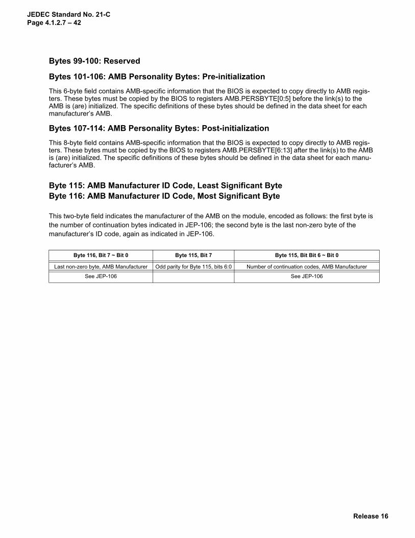
Bytes 99-100: Reserved
Bytes 101-106: AMB Personality Bytes: Pre-initializationThis 6-byte field contains AMB-specific information that the BIOS is expected to copy directly to AMB regis-ters. These bytes must be copied by the BIOS to registers AMB.PERSBYTE[0:5] before the link(s) to the AMB is (are) initialized. The specific definitions of these bytes should be defined in the data sheet for each manufacturer’s AMB.
Bytes 107-114: AMB Personality Bytes: Post-initializationThis 8-byte field contains AMB-specific information that the BIOS is expected to copy directly to AMB regis-ters. These bytes must be copied by the BIOS to registers AMB.PERSBYTE[6:13] after the link(s) to the AMB is (are) initialized. The specific definitions of these bytes should be defined in the data sheet for each manu-facturer’s AMB.
Byte 115: AMB Manufacturer ID Code, Least Significant ByteByte 116: AMB Manufacturer ID Code, Most Significant Byte
This two-byte field indicates the manufacturer of the AMB on the module, encoded as follows: the first byte is the number of continuation bytes indicated in JEP-106; the second byte is the last non-zero byte of the manufacturer’s ID code, again as indicated in JEP-106.
Byte 116, Bit 7 ~ Bit 0 Byte 115, Bit 7 Byte 115, Bit Bit 6 ~ Bit 0
Last non-zero byte, AMB Manufacturer Odd parity for Byte 115, bits 6:0 Number of continuation codes, AMB Manufacturer
See JEP-106 See JEP-106
Release 16

Relea
JEDEC Standard No. 21-CPage 4.1.2.7– 43
2.3 Unique Module ID: Bytes 117 to 125
Byte 117: Module Manufacturer ID Code, Least Significant ByteByte 118: Module Manufacturer ID Code, Most Significant Byte
This two-byte field indicates the manufacturer of the module, encoded as follows: the first byte is the number of continuation bytes indicated in JEP-106; the second byte is the last non-zero byte of the manufacturer’s ID code, again as indicated in JEP-106.
Byte 119: Module Manufacturing Location
The module manufacturer includes an identifier that uniquely defines the manufacturing location of the mem-ory module. While the SPD spec will not attempt to present a decode table for manufacturing sites, the indi-vidual manufacturer may keep track of manufacturing location and its appropriate decode represented in this byte.
Bytes 120-121: Module Manufacturing Date
The module manufacturer includes a date code for the module. The JEDEC definitions for bytes 120 and 121 are year and week respectively. These bytes must be represented in Binary Coded Decimal (BCD). For example, week 47 in year 2003 would be coded as 03 (0000 0011) in byte 120 and 47 (0100 0111) in byte 121.
Bytes 122-125: Module Serial Number
The supplier must include a unique serial number for the module. The supplier may use whatever decode method desired to maintain a unique serial number for each module.
One method of achieving this is by assigning a byte in the field from 122-125 as a tester ID byte and using the remaining bytes as a sequential serial number. Bytes 117-125 will then result in a nine-byte unique module identifier. Note that part number is not included in this identifier: the supplier may not give the same value for Bytes 119:125 to more than one DIMM even if the DIMMs have different part numbers.
Byte 118, Bit 7 ~ Bit 0 Byte 117, Bit 7 Byte 117, Bit Bit 6 ~ Bit 0
Last non-zero byte, Module Manufacturer Odd parity for Byte 117, bits 6:0 Number of continuation codes, Module Manufacturer
See JEP-106 See JEP-106
se 16

JEDEC Standard No. 21-CPage 4.1.2.7 – 44
2.4 CRC: Bytes 126 to 127
Bytes 126-127: SPD Cyclical Redundancy Code (CRC)
This two-byte field contains the calculated 16-bit CRC-CCITT (polynomial 0x1021) for previous bytes in the SPD. The following algorithm and data structures (shown in C) are to be followed in calculating and checking the code. Bit 7 of Byte 0 indicates which bytes are covered by the CRC. The polynomial calculated with this algorithm is x16 + x12 + x5 + 1.
int Crc16 (char *ptr, int count){
int crc, i;
crc = 0;while (--count >= 0) {
crc = crc ^ (int)*ptr++ << 8;for (i = 0; i < 8; ++i)
if (crc & 0x8000) crc = crc << 1 ^ 0x1021;
else crc = crc << 1;
}return (crc & 0xFFFF);
}
char spdBytes[] = { SPD_byte_0, SPD_byte_1, ..., SPD_byte_N-1 };int data16;
data16 = Crc16 (spdBytes, sizeof(spdBytes));SPD_byte_126 = (char) (data16 & 0xFF);SPD_byte_127 = (char) (data16 >> 8);
Release 16

Relea
JEDEC Standard No. 21-CPage 4.1.2.7– 45
2.5 Other Manufacturer Fields and User Space: Bytes 128 to 255
Bytes 128-145: Module Part Number
The manufacturer’s part number is written in ASCII format within these bytes. Unused digits are coded as ASCII blanks (0x20).
Bytes 146-147: Module Revision Code
This refers to the module revision code. While the SPD spec will not attempt to define the format for this infor-mation, the individual manufacturer may keep track of the revision code and its appropriate decode repre-sented in this byte.
Byte 148: SDRAM Manufacturer ID Code, Least Significant ByteByte 149: SDRAM Manufacturer ID Code, Most Significant Byte
This two-byte field indicates the manufacturer of the SDRAM on the module, encoded as follows: the first byte is the number of continuation bytes indicated in JEP-106; the second byte is the last non-zero byte of the manufacturer’s ID code, again as indicated in JEP-106.
Bytes 150-175: Manufacturer’s Specific Data
The module manufacturer may include any additional information desired into the module within these loca-tions.
Bytes 176-255: Open for Customer Use
These bytes are unused by the manufacturer and are open for customer use.
Byte 149, Bit 7 ~ Bit 0 Byte 148, Bit 7 Byte 148, Bit Bit 6 ~ Bit 0
Last non-zero byte, Module Manufacturer Odd parity for Byte 148, bits 6:0 Number of continuation codes, Module Manufacturer
See JEP-106 See JEP-106
se 16

Release 16
JEDEC Standard No. 21-CPage 4.1.2.7 – 46
Appendix: ASCII Decode Matrix for SPDs
The following table is a subset of the full ASCII standard which is used for coding bytes in the Serial Presence Detect EEPROM that require ASCII characters:
Examples:0x20 = Blank Space0x34 = 40x41 = A
Second Hex Digit in Pair
First HexDigit in Pair 0 1 2 3 4 5 6 7 8 9 A B C D E F
2 BlankSpace ( ) -
Dash .
3 0 1 2 3 4 5 6 7 8 9
4 A B C D E F G H I J K L M N O
5 P Q R S T U V W X Y Z
6 a b c d e f g h i j k l m n o
7 p q r s t u v w x y z
SPD Bytes 128-145
Manufacturer’s PN Coded in ASCII
13M32734BCD-260Y 31334D33323733344243442D323630592020

Release 16
JEDEC Standard No. 21-CPage 4.1.2.7– 47
Revision Log Date Rev Pages Contents of Modification
Mar. 2006 1.111 Extended range of CL
15 Extended range of AL and WL
Jan. 2006 1.1
42 Added byte 98 (AMB Tjmax)
32 Added byte 79 (Required ODT)
28 Clarified sub-field indicators
25 Corrected values for SPD entries, byte 35 (DT0)
5 Changed revision from 1.0 to 1.1
Jan. 2005 1.0 All Initial release