any other way to nand2 implementation?
TRANSCRIPT
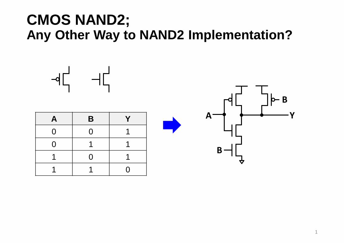
CMOS NAND2; Any Other Way to NAND2 Implementation?
1
A B Y
0 0 1
0 1 1
1 0 1
1 1 0
A
B
B
Y
Contents
• Pseudo nMOS
• Cascode Voltage Switch Logic
• Dynamic Circuit and Domino Logic
• Pass-Transistor Circuits
3

Pseudo nMOS Constructing logic only with pull-down network
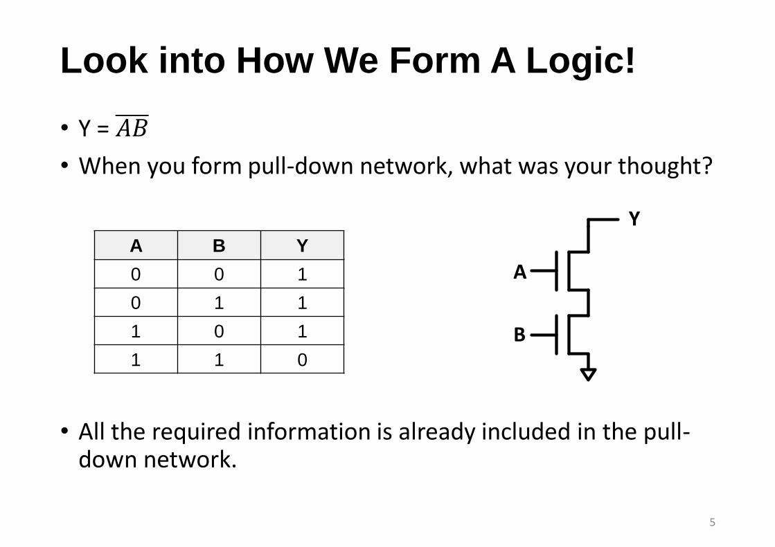
Look into How We Form A Logic!
• Y = 𝐴𝐵
• When you form pull-down network, what was your thought?
• All the required information is already included in the pull-down network.
5
A B Y
0 0 1
0 1 1
1 0 1
1 1 0
A
B
Y
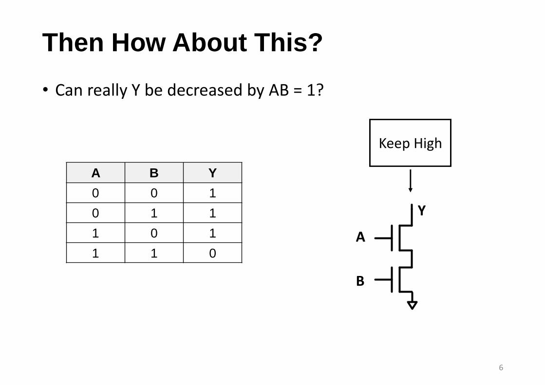
Then How About This?
• Can really Y be decreased by AB = 1?
6
A B Y
0 0 1
0 1 1
1 0 1
1 1 0
Keep High
A
B
Y
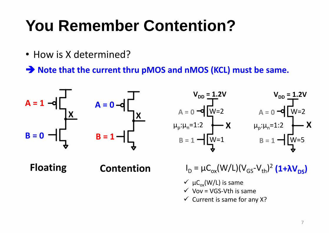
You Remember Contention?
• How is X determined?
Note that the current thru pMOS and nMOS (KCL) must be same.
7
A = 1
B = 0
X
Floating
A = 0
B = 1
X
Contention ID = μCox(W/L)(VGS-Vth)2
A = 0
B = 1
W=2
W=1
μp:μn=1:2
VDD = 1.2V
A = 0
B = 1
W=2
W=5
μp:μn=1:2
VDD = 1.2V
(1+λVDS)
μCox(W/L) is same Vov = VGS-Vth is same Current is same for any X?
X X
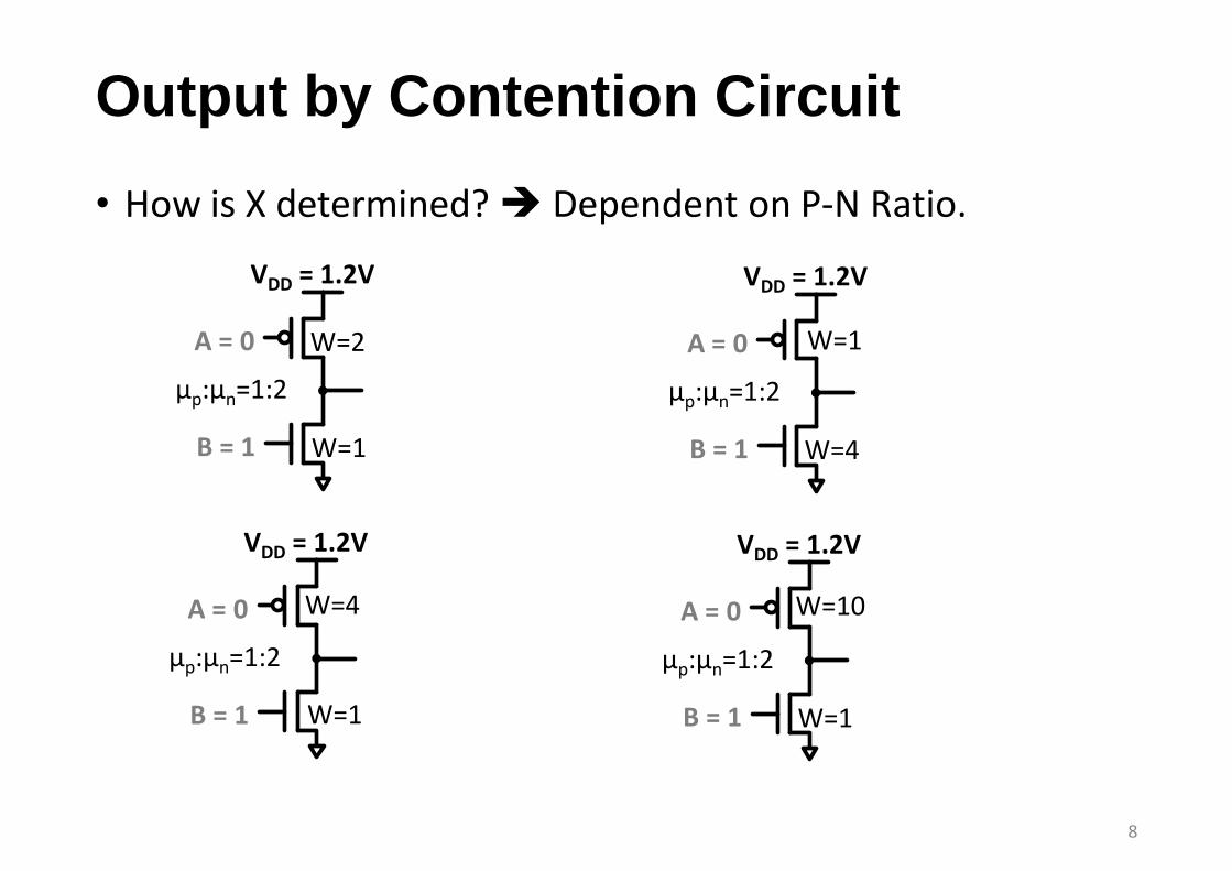
Output by Contention Circuit
• How is X determined? Dependent on P-N Ratio.
8
A = 0
B = 1
W=2
W=1
μp:μn=1:2
VDD = 1.2V
A = 0
B = 1
W=1
W=4
μp:μn=1:2
VDD = 1.2V
A = 0
B = 1
W=4
W=1
μp:μn=1:2
VDD = 1.2V
A = 0
B = 1
W=10
W=1
μp:μn=1:2
VDD = 1.2V
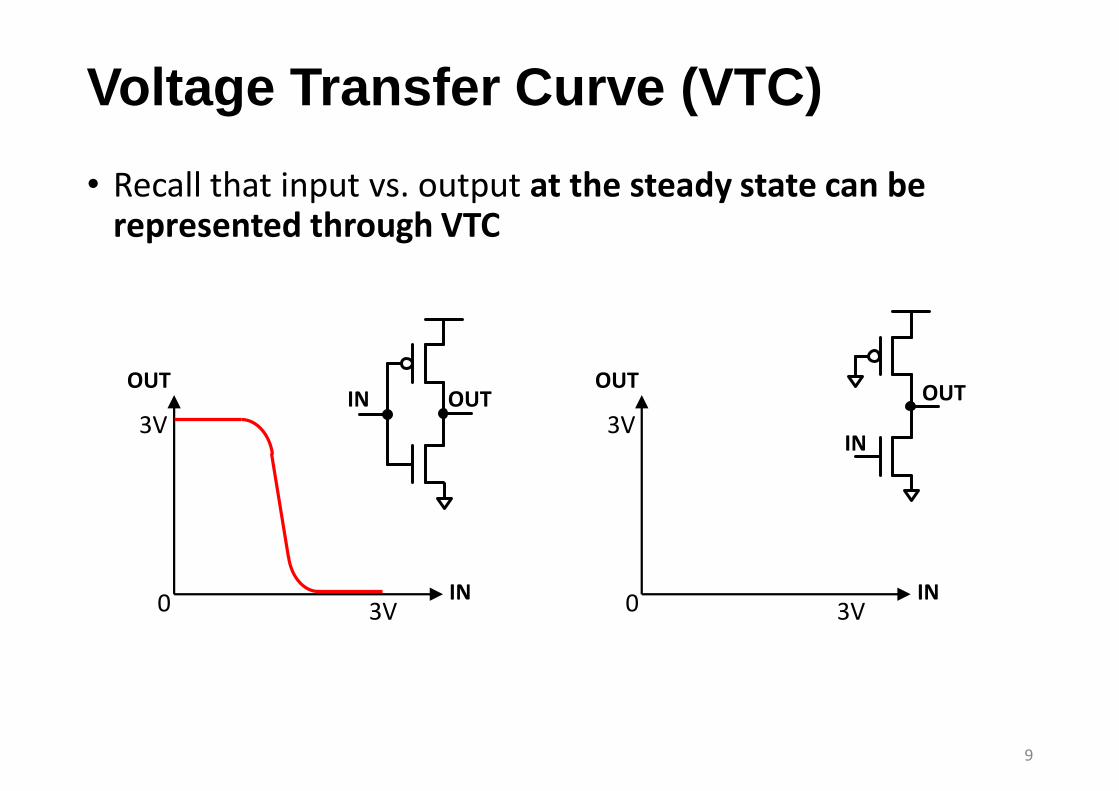
Voltage Transfer Curve (VTC)
• Recall that input vs. output at the steady state can be represented through VTC
9
IN
OUT
3V
3V0 IN
OUT
3V
3V0
IN OUT
IN
OUT
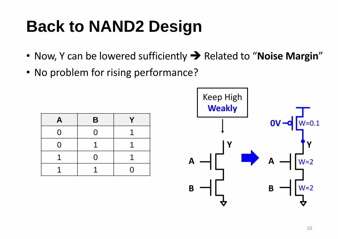
Back to NAND2 Design
• Now, Y can be lowered sufficiently Related to “Noise Margin”
• No problem for rising performance?
10
A B Y
0 0 1
0 1 1
1 0 1
1 1 0
Keep High
A
B
Y
Weakly
A
B
Y
0V W=0.1
W=2
W=2
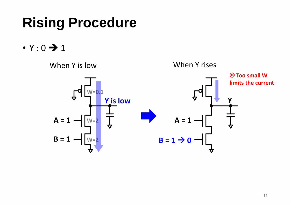
Rising Procedure
• Y : 0 1
11
Y
A = 1
B = 1 0
Y is low
A = 1
B = 1
When Y is low When Y rises
W=0.1
W=2
W=2
Too small W limits the current
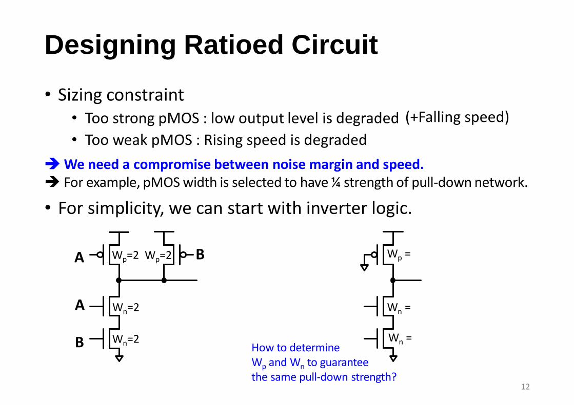
Designing Ratioed Circuit
• Sizing constraint• Too strong pMOS : low output level is degraded
• Too weak pMOS : Rising speed is degraded
We need a compromise between noise margin and speed. For example, pMOS width is selected to have ¼ strength of pull-down network.
• For simplicity, we can start with inverter logic.
12
(+Falling speed)
How to determineWp and Wn to guaranteethe same pull-down strength?
A
B
A B
Wn=2
Wn=2
Wp=2 Wp=2
Wn =
Wn =
Wp =
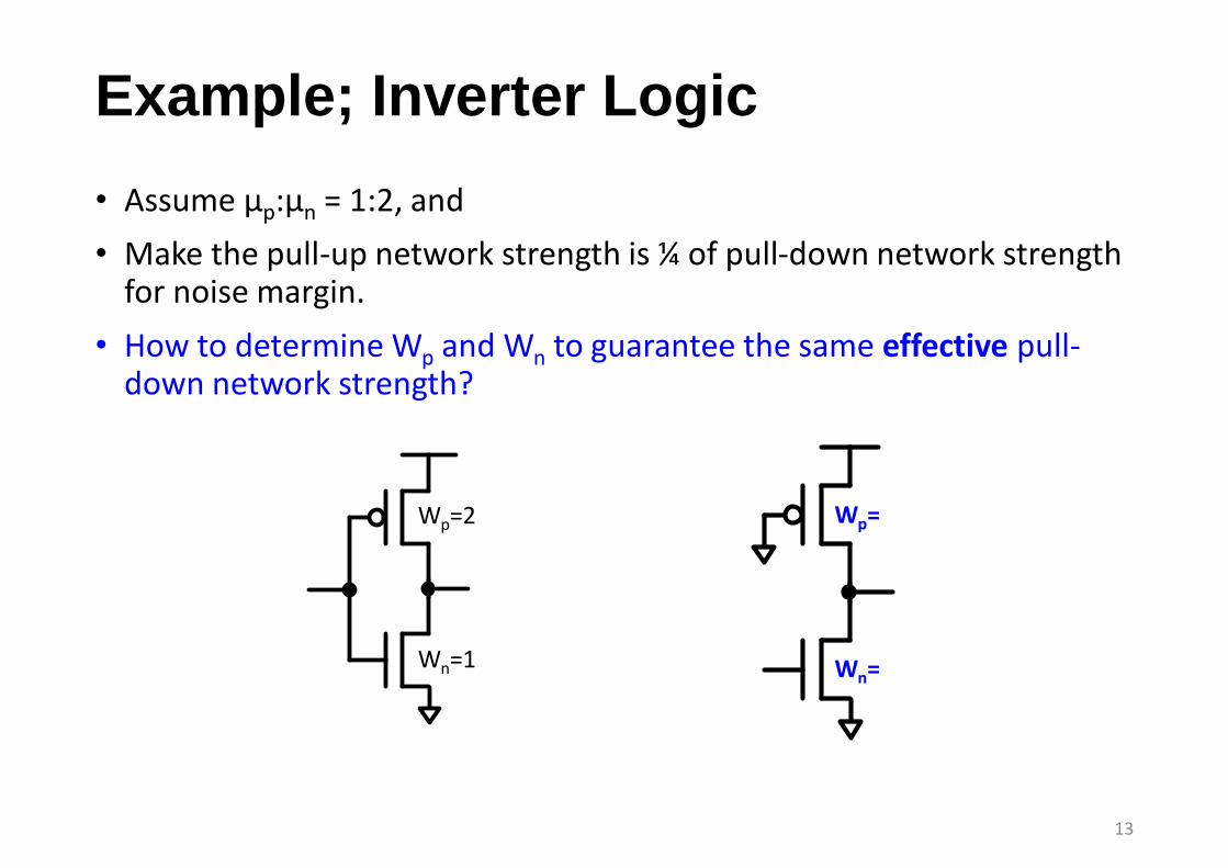
Example; Inverter Logic
• Assume μp:μn = 1:2, and
• Make the pull-up network strength is ¼ of pull-down network strength for noise margin.
• How to determine Wp and Wn to guarantee the same effective pull-down network strength?
13
Wp=2
Wn=1
Wp=
Wn=
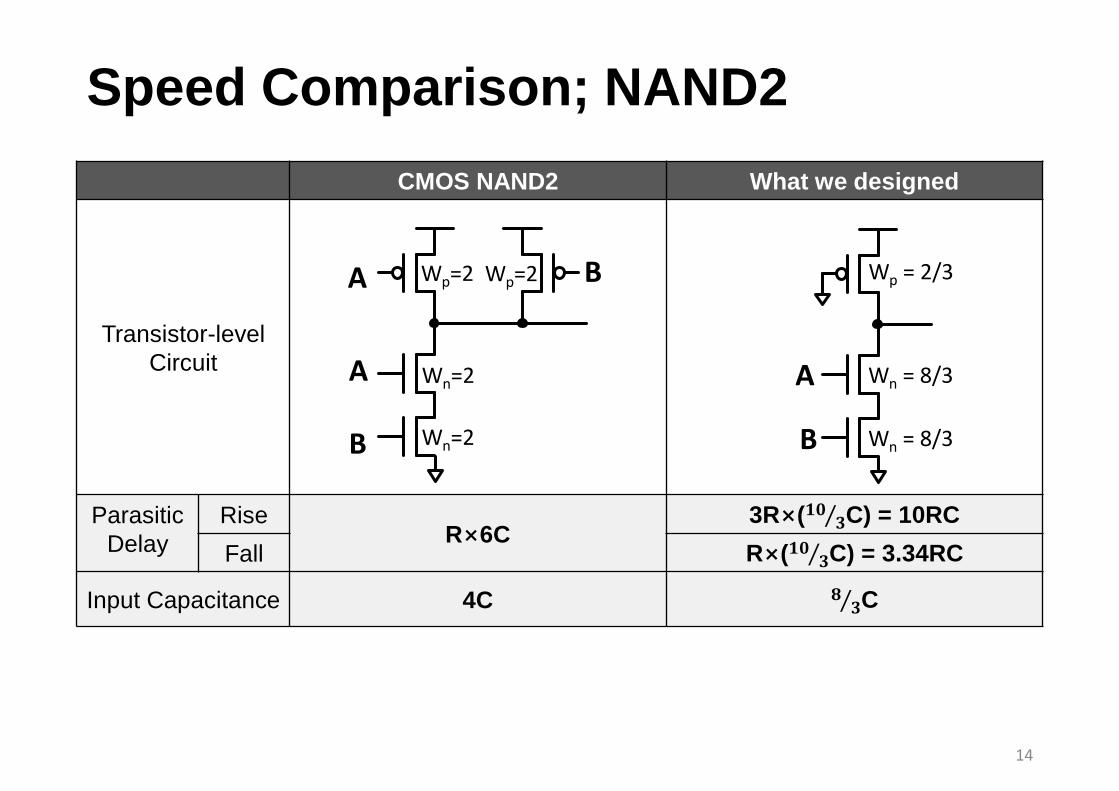
Speed Comparison; NAND2
CMOS NAND2 What we designed
Transistor-level
Circuit
Parasitic
Delay
RiseR×6C
3R×( 𝟏𝟎𝟑C) = 10RC
Fall R×( 𝟏𝟎𝟑C) = 3.34RC
Input Capacitance 4C 𝟖 𝟑C
14
A
B
A B
Wn=2
Wn=2
Wp=2 Wp=2
Wn = 8/3
Wn = 8/3
Wp = 2/3
A
B
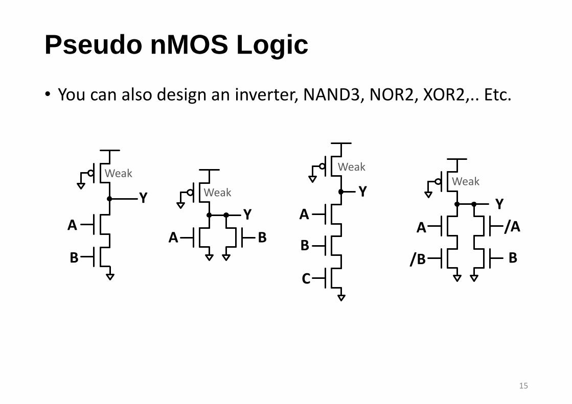
Pseudo nMOS Logic
• You can also design an inverter, NAND3, NOR2, XOR2,.. Etc.
15
Weak
A
B
Weak
A B
YY Y
A
B
C
Y
A
/B
/A
B
WeakWeak
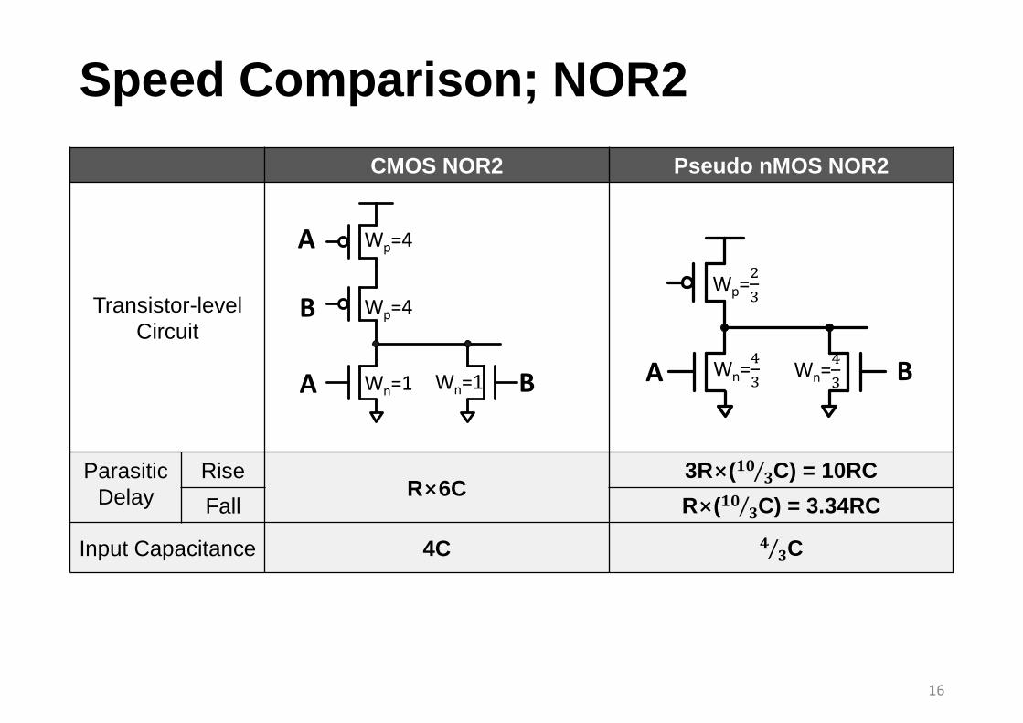
CMOS NOR2 Pseudo nMOS NOR2
Transistor-level
Circuit
Parasitic
Delay
RiseR×6C
3R×( 𝟏𝟎𝟑C) = 10RC
Fall R×( 𝟏𝟎𝟑C) = 3.34RC
Input Capacitance 4C 𝟒 𝟑C
Speed Comparison; NOR2
16
A
B
A
Wn=1
Wp=4
Wp=4
BWn=1Wn=
4
3A BWn=4
3
Wp=2
3
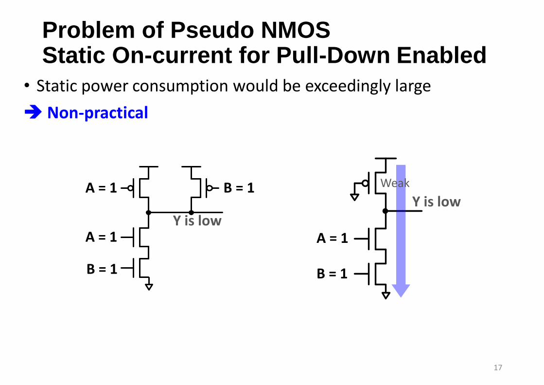
Problem of Pseudo NMOSStatic On-current for Pull-Down Enabled
• Static power consumption would be exceedingly large
Non-practical
17
Y is low
A = 1
B = 1
A = 1
B = 1
A = 1 B = 1
Y is low
Weak
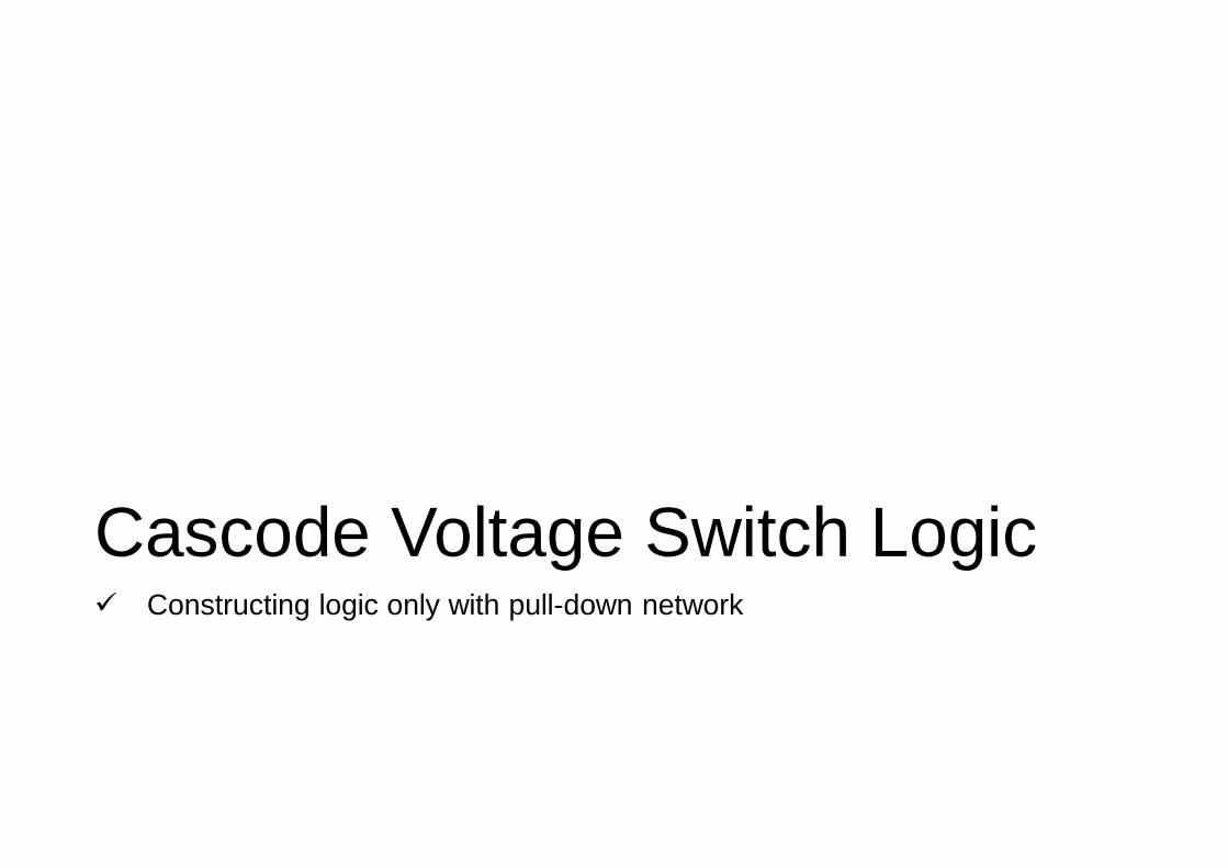
Cascode Voltage Switch Logic Constructing logic only with pull-down network
Revisit Pseudo nMOS NAND2
• Is there any way to block pull-up when Y is to be low by A=1 and B=1?
19
Y is low
A = 1
B = 1
Weak
A = 1
B = 1
XY is low
X should risewhen Y is low
𝒀
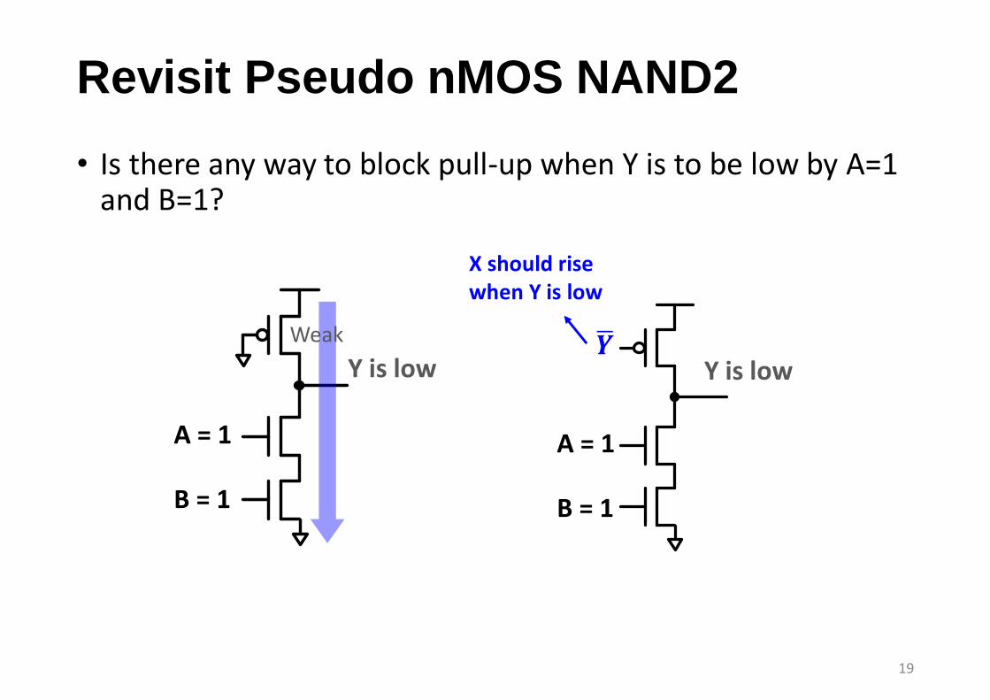
Generating Complementary Output
• How can we generate 𝑌?
20
A = 1
B = 1
Y = 𝑨𝑩 𝒀
= AB?
𝑨 𝑩
=AB
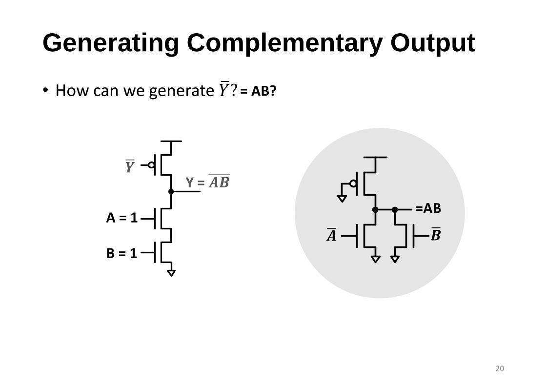
Combining Two Pseudo NMOS
• We call this type logic as cascade voltage switch logic (CVSL).
21
A
B/A /B
A
B/A /B
Y /Y
Cross-coupled PFET
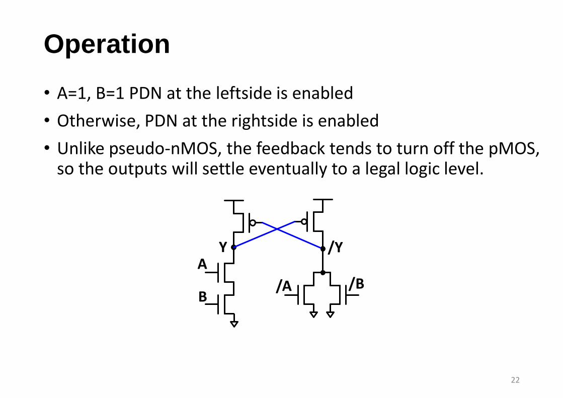
Operation
• A=1, B=1 PDN at the leftside is enabled
• Otherwise, PDN at the rightside is enabled
• Unlike pseudo-nMOS, the feedback tends to turn off the pMOS, so the outputs will settle eventually to a legal logic level.
22
A
B/A /B
Y /Y
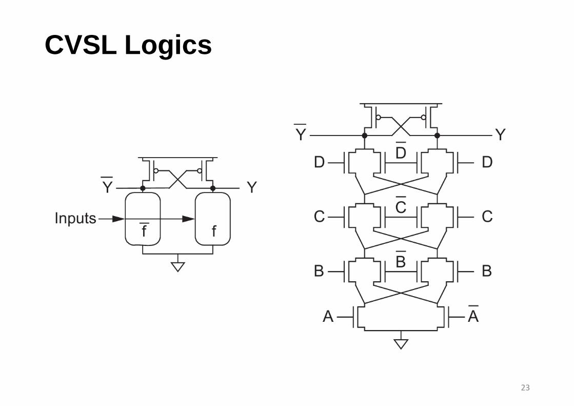
CVSL Logics
23

How Does Cross-coupled FET Operate?
• You also saw this structure in the level shifter
• It operates in the positive feedback manner.
24
VDDH VDDH
VDDL
IN INB
OUTXL A
B/A /B
Y /Y
Level Shifter CVSL