ansoft hfss fundamentals - url.t · p01simplorer power electronics p01-‹#› v10 simplorer v10...
TRANSCRIPT
P01
Power Electronics
P01-‹#›
Simplorer v10
Simplorer v10 User’s Guide
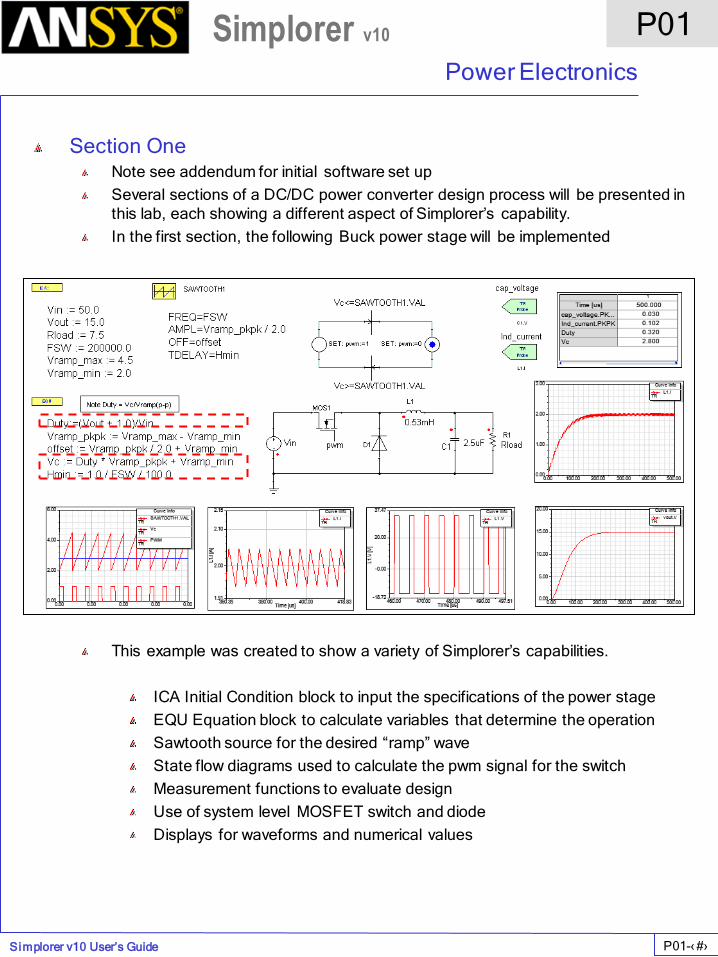
Section One Note see addendum for initial software set up
Several sections of a DC/DC power converter design process will be presented in
this lab, each showing a different aspect of Simplorer’s capability.
In the first section, the following Buck power stage will be implemented
This example was created to show a variety of Simplorer’s capabilities.
ICA Initial Condition block to input the specifications of the power stage
EQU Equation block to calculate variables that determine the operation
Sawtooth source for the desired “ramp” wave
State flow diagrams used to calculate the pwm signal for the switch
Measurement functions to evaluate design
Use of system level MOSFET switch and diode
Displays for waveforms and numerical values
P01
Power Electronics
P01-‹#›
Simplorer v10
Simplorer v10 User’s Guide
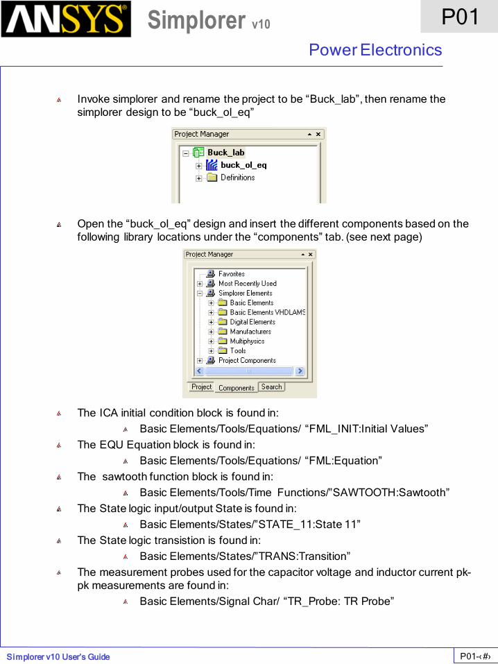
Invoke simplorer and rename the project to be “Buck_lab”, then rename the
simplorer design to be “buck_ol_eq”
Open the “buck_ol_eq” design and insert the different components based on the
following library locations under the “components” tab. (see next page)
The ICA initial condition block is found in:
Basic Elements/Tools/Equations/ “FML_INIT:Initial Values”
The EQU Equation block is found in:
Basic Elements/Tools/Equations/ “FML:Equation”
The sawtooth function block is found in:
Basic Elements/Tools/Time Functions/”SAWTOOTH:Sawtooth”
The State logic input/output State is found in:
Basic Elements/States/”STATE_11:State 11”
The State logic transistion is found in:
Basic Elements/States/”TRANS:Transition”
The measurement probes used for the capacitor voltage and inductor current pk-
pk measurements are found in:
Basic Elements/Signal Char/ “TR_Probe: TR Probe”
P01
Power Electronics
P01-‹#›
Simplorer v10
Simplorer v10 User’s Guide
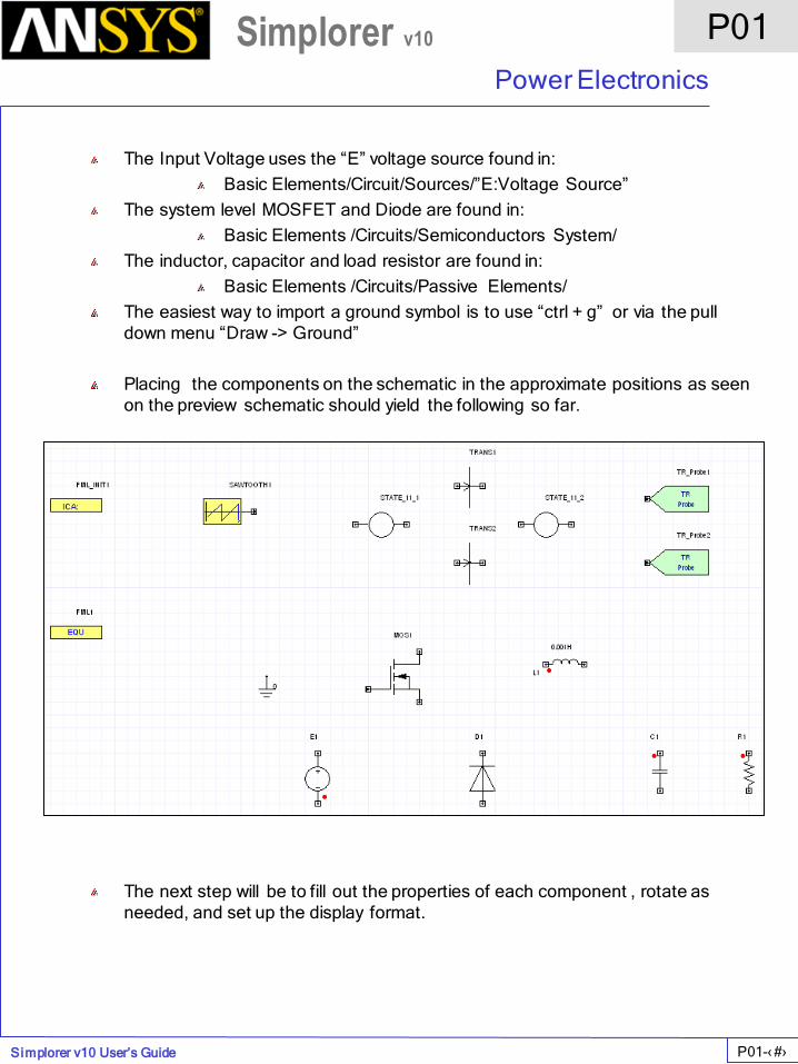
The Input Voltage uses the “E” voltage source found in:
Basic Elements/Circuit/Sources/”E:Voltage Source”
The system level MOSFET and Diode are found in:
Basic Elements /Circuits/Semiconductors System/
The inductor, capacitor and load resistor are found in:
Basic Elements /Circuits/Passive Elements/
The easiest way to import a ground symbol is to use “ctrl + g” or via the pull
down menu “Draw -> Ground”
Placing the components on the schematic in the approximate positions as seen
on the preview schematic should yield the following so far.
The next step will be to fill out the properties of each component , rotate as
needed, and set up the display format.

P01
Power Electronics
P01-‹#›
Simplorer v10
Simplorer v10 User’s Guide
Setting up the ICA block:
Double click on the ICA block, add in variables via the standard
“input” Icon for each variable to be added. Make sure to select the “Show”
box to display the variable on the schematic. De-select the “Show Name”
for the “Name” of the ICA block. It should look like the following:
Select “OK”
To resize the text on the schematic, select all the variables by holding the
left mouse button down while drawing a box around all the variables, they
will turn red to indicate the selection. Note in the “Properties” window on
the left side of the Simplorer window has a selection called “PropDisplay
Font Size”, by default it is set to 5. change it to 12, select the “Enter” key.
To reset the spacing, change the
“PropDisplay Location” from Bottom
To Center, then back to Bottom. It should
Now look as follows.
P01
Power Electronics
P01-‹#›
Simplorer v10
Simplorer v10 User’s Guide
Note the values in the ICA block represents the following:
Vin = input voltage
Vout = output voltage
FSW = switching frequency
Vramp_max and Vramp_min represents the typical ramp voltage range
found in PWM IC Controllers. this is used to compare to the “control
voltage” Vc that comes from the typical error amplifier found in a normal
feedback loop.
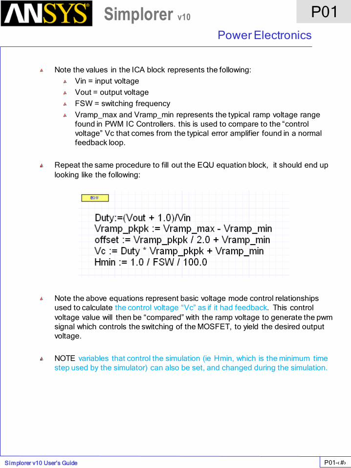
Repeat the same procedure to fill out the EQU equation block, it should end up
looking like the following:
Note the above equations represent basic voltage mode control relationships
used to calculate the control voltage “Vc” as if it had feedback. This control
voltage value will then be “compared” with the ramp voltage to generate the pwm
signal which controls the switching of the MOSFET, to yield the desired output
voltage.
NOTE variables that control the simulation (ie Hmin, which is the minimum time
step used by the simulator) can also be set, and changed during the simulation.
P01
Power Electronics
P01-‹#›
Simplorer v10
Simplorer v10 User’s Guide
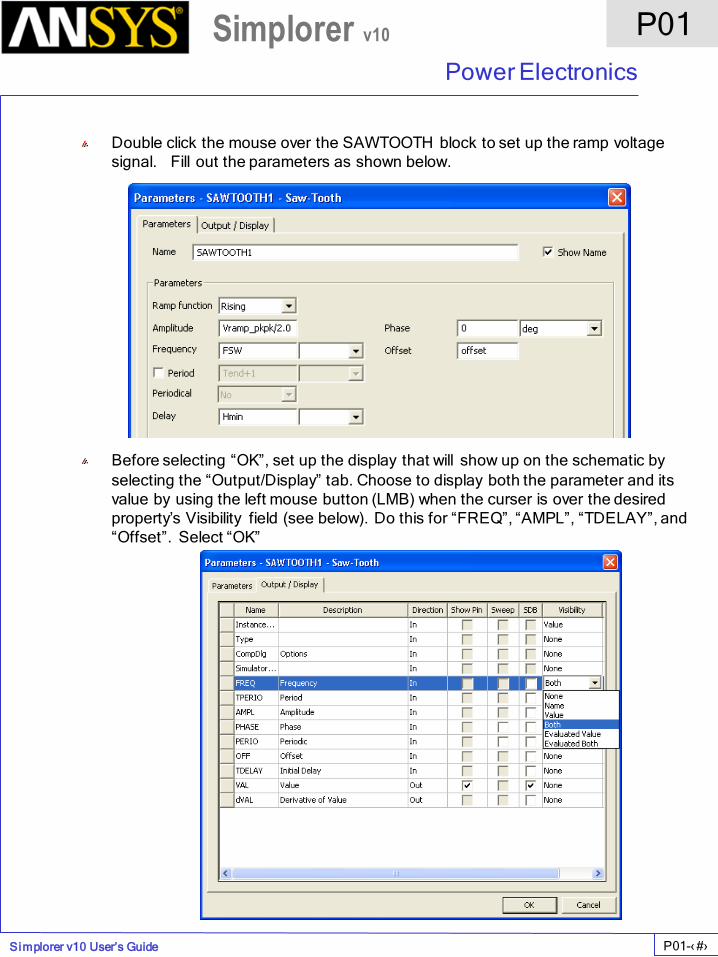
Double click the mouse over the SAWTOOTH block to set up the ramp voltage
signal. Fill out the parameters as shown below.
Before selecting “OK”, set up the display that will show up on the schematic by
selecting the “Output/Display” tab. Choose to display both the parameter and its
value by using the left mouse button (LMB) when the curser is over the desired
property’s Visibility field (see below). Do this for “FREQ”, “AMPL”, “TDELAY”, and
“Offset”. Select “OK”
P01
Power Electronics
P01-‹#›
Simplorer v10
Simplorer v10 User’s Guide
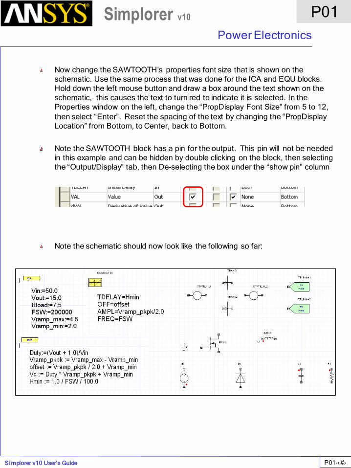
Now change the SAWTOOTH’s properties font size that is shown on the
schematic. Use the same process that was done for the ICA and EQU blocks.
Hold down the left mouse button and draw a box around the text shown on the
schematic, this causes the text to turn red to indicate it is selected. In the
Properties window on the left, change the “PropDisplay Font Size” from 5 to 12,
then select “Enter”. Reset the spacing of the text by changing the “PropDisplay
Location” from Bottom, to Center, back to Bottom.
Note the SAWTOOTH block has a pin for the output. This pin will not be needed
in this example and can be hidden by double clicking on the block, then selecting
the “Output/Display” tab, then De-selecting the box under the “show pin” column
Note the schematic should now look like the following so far:
P01
Power Electronics
P01-‹#›
Simplorer v10
Simplorer v10 User’s Guide
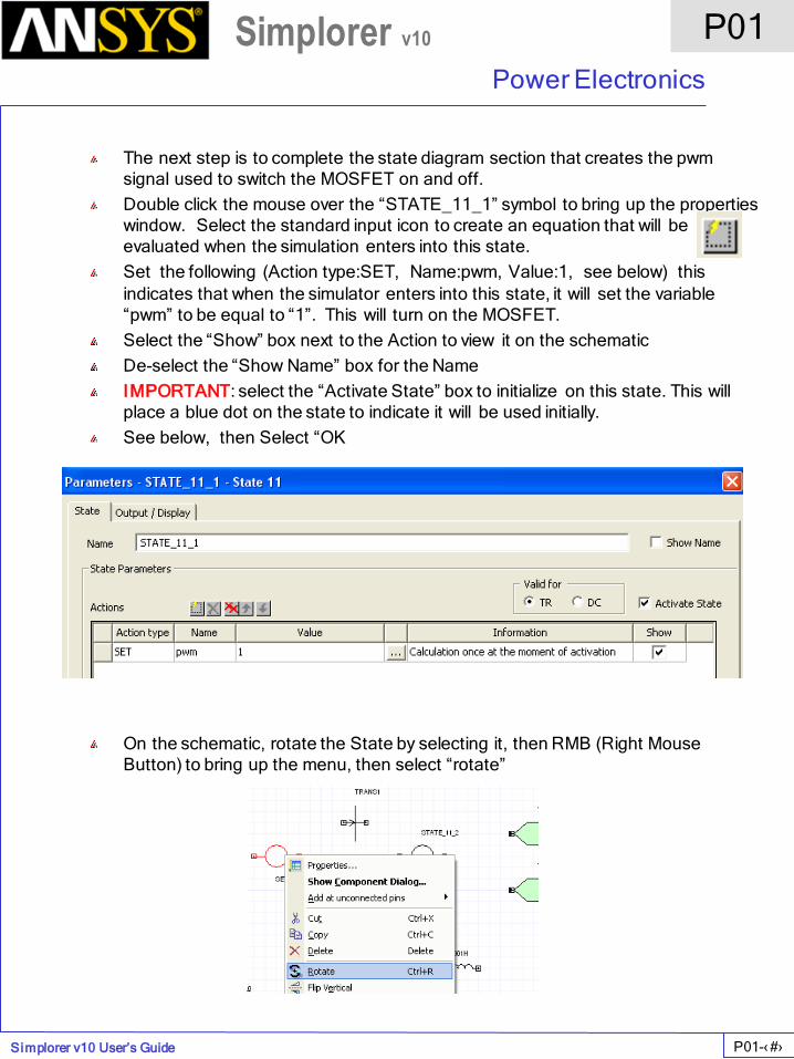
The next step is to complete the state diagram section that creates the pwm
signal used to switch the MOSFET on and off.
Double click the mouse over the “STATE_11_1” symbol to bring up the properties
window. Select the standard input icon to create an equation that will be
evaluated when the simulation enters into this state.
Set the following (Action type:SET, Name:pwm, Value:1, see below) this
indicates that when the simulator enters into this state, it will set the variable
“pwm” to be equal to “1”. This will turn on the MOSFET.
Select the “Show” box next to the Action to view it on the schematic
De-select the “Show Name” box for the Name
IMPORTANT: select the “Activate State” box to initialize on this state. This will
place a blue dot on the state to indicate it will be used initially.
See below, then Select “OK
On the schematic, rotate the State by selecting it, then RMB (Right Mouse
Button) to bring up the menu, then select “rotate”
P01
Power Electronics
P01-‹#›
Simplorer v10
Simplorer v10 User’s Guide
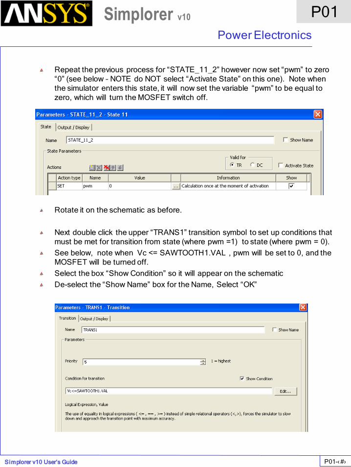
Repeat the previous process for “STATE_11_2” however now set “pwm” to zero
“0” (see below – NOTE do NOT select “Activate State” on this one). Note when
the simulator enters this state, it will now set the variable “pwm” to be equal to
zero, which will turn the MOSFET switch off.
Rotate it on the schematic as before.
Next double click the upper “TRANS1” transition symbol to set up conditions that
must be met for transition from state (where pwm =1) to state (where pwm = 0).
See below, note when Vc <= SAWTOOTH1.VAL , pwm will be set to 0, and the
MOSFET will be turned off.
Select the box “Show Condition” so it will appear on the schematic
De-select the “Show Name” box for the Name, Select “OK”
P01
Power Electronics
P01-‹#›
Simplorer v10
Simplorer v10 User’s Guide
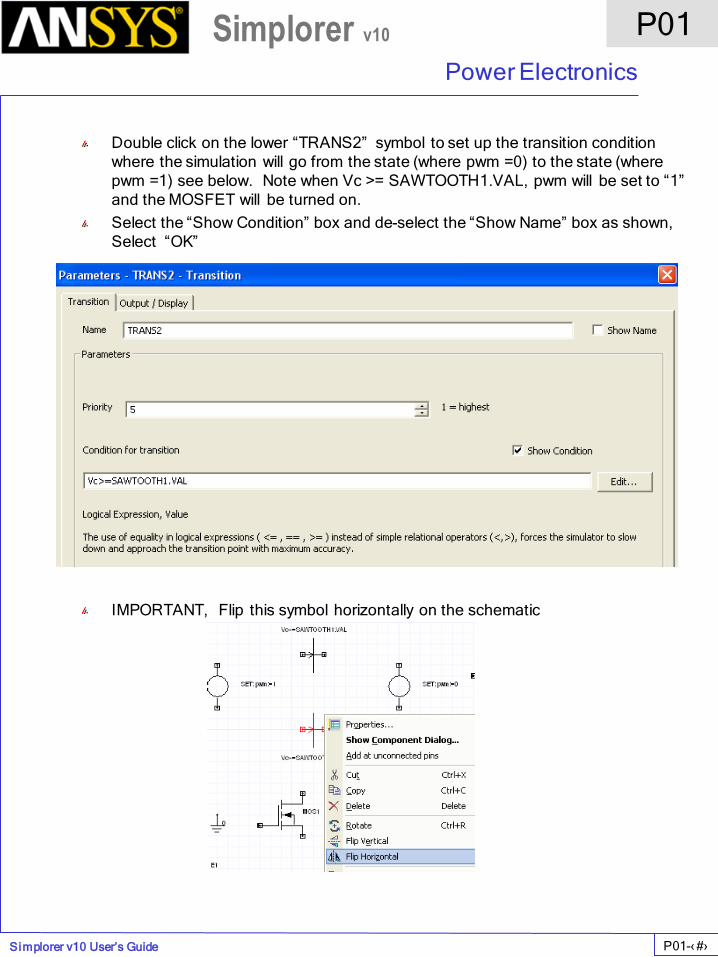
Double click on the lower “TRANS2” symbol to set up the transition condition
where the simulation will go from the state (where pwm =0) to the state (where
pwm =1) see below. Note when Vc >= SAWTOOTH1.VAL, pwm will be set to “1”
and the MOSFET will be turned on.
Select the “Show Condition” box and de-select the “Show Name” box as shown,
Select “OK”
IMPORTANT, Flip this symbol horizontally on the schematic
P01
Power Electronics
P01-‹#›
Simplorer v10
Simplorer v10 User’s Guide
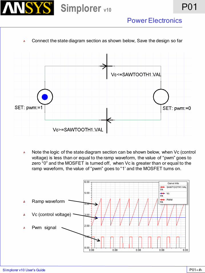
Connect the state diagram section as shown below, Save the design so far
Note the logic of the state diagram section can be shown below, when Vc (control
voltage) is less than or equal to the ramp waveform, the value of “pwm” goes to
zero “0” and the MOSFET is turned off, when Vc is greater than or equal to the
ramp waveform, the value of “pwm” goes to “1’ and the MOSFET turns on.
Ramp waveform
Vc (control voltage)
Pwm signal

P01
Power Electronics
P01-‹#›
Simplorer v10
Simplorer v10 User’s Guide
Next step is to configure the power stage electronics
Double click on the voltage source and assign the variable “Vin” as seen below.
Remember this value of “Vin” comes from the ICA initial condition block. Select
the “Spice compatible” box (for spice compatible sign convention)
Select the “Output/Display” tab and using the left mouse button, make the EMF
Value visible as shown below, Select “OK”
P01
Power Electronics
P01-‹#›
Simplorer v10
Simplorer v10 User’s Guide
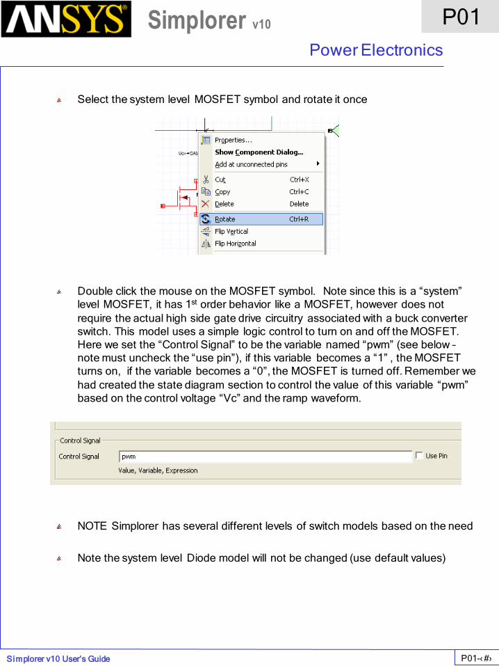
Select the system level MOSFET symbol and rotate it once
Double click the mouse on the MOSFET symbol. Note since this is a “system”
level MOSFET, it has 1st order behavior like a MOSFET, however does not
require the actual high side gate drive circuitry associated with a buck converter
switch. This model uses a simple logic control to turn on and off the MOSFET.
Here we set the “Control Signal” to be the variable named “pwm” (see below –
note must uncheck the “use pin”), if this variable becomes a “1” , the MOSFET
turns on, if the variable becomes a “0”, the MOSFET is turned off. Remember we
had created the state diagram section to control the value of this variable “pwm”
based on the control voltage “Vc” and the ramp waveform.
NOTE Simplorer has several different levels of switch models based on the need
Note the system level Diode model will not be changed (use default values)
P01
Power Electronics
P01-‹#›
Simplorer v10
Simplorer v10 User’s Guide
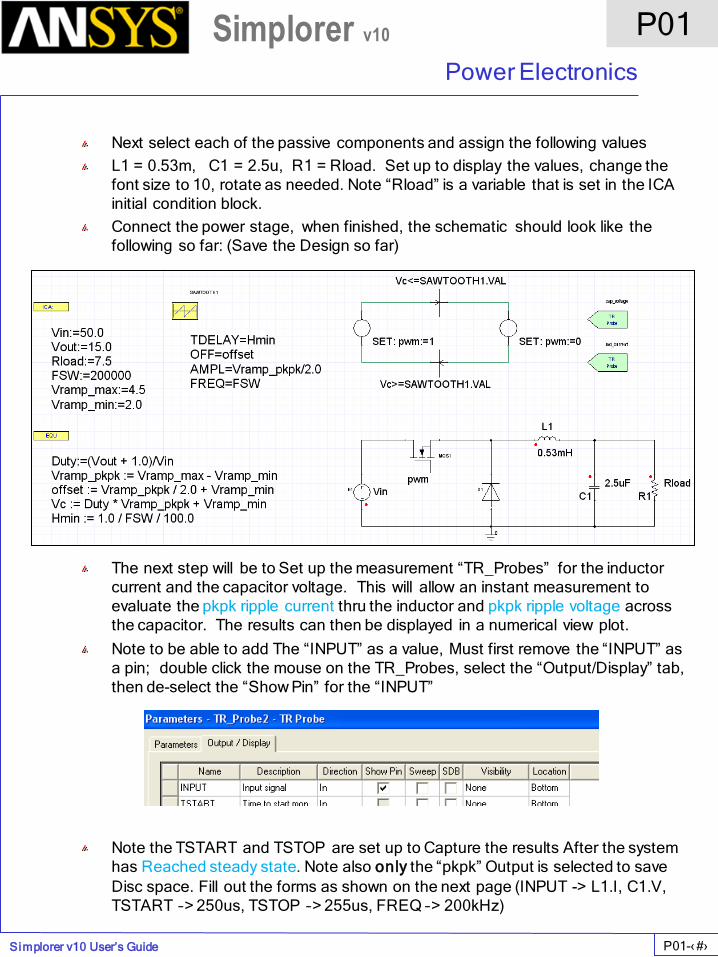
Next select each of the passive components and assign the following values
L1 = 0.53m, C1 = 2.5u, R1 = Rload. Set up to display the values, change the
font size to 10, rotate as needed. Note “Rload” is a variable that is set in the ICA
initial condition block.
Connect the power stage, when finished, the schematic should look like the
following so far: (Save the Design so far)
The next step will be to Set up the measurement “TR_Probes” for the inductor
current and the capacitor voltage. This will allow an instant measurement to
evaluate the pkpk ripple current thru the inductor and pkpk ripple voltage across
the capacitor. The results can then be displayed in a numerical view plot.
Note to be able to add The “INPUT” as a value, Must first remove the “INPUT” as
a pin; double click the mouse on the TR_Probes, select the “Output/Display” tab,
then de-select the “Show Pin” for the “INPUT”
Note the TSTART and TSTOP are set up to Capture the results After the system
has Reached steady state. Note also only the “pkpk” Output is selected to save
Disc space. Fill out the forms as shown on the next page (INPUT -> L1.I, C1.V,
TSTART –> 250us, TSTOP –> 255us, FREQ –> 200kHz)
P01
Power Electronics
P01-‹#›
Simplorer v10
Simplorer v10 User’s Guide
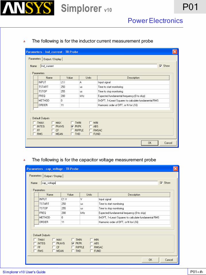
The following is for the inductor current measurement probe
The following is for the capacitor voltage measurement probe
P01
Power Electronics
P01-‹#›
Simplorer v10
Simplorer v10 User’s Guide
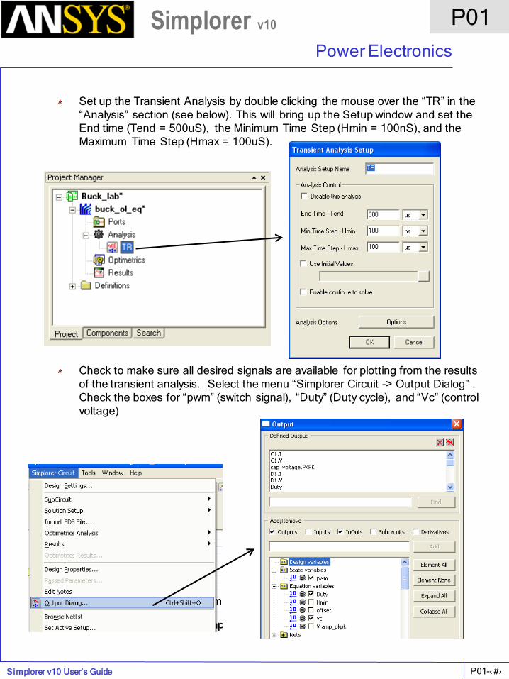
Set up the Transient Analysis by double clicking the mouse over the “TR” in the
“Analysis” section (see below). This will bring up the Setup window and set the
End time (Tend = 500uS), the Minimum Time Step (Hmin = 100nS), and the
Maximum Time Step (Hmax = 100uS).
Check to make sure all desired signals are available for plotting from the results
of the transient analysis. Select the menu “Simplorer Circuit -> Output Dialog” .
Check the boxes for “pwm” (switch signal), “Duty” (Duty cycle), and “Vc” (control
voltage)
P01
Power Electronics
P01-‹#›
Simplorer v10
Simplorer v10 User’s Guide
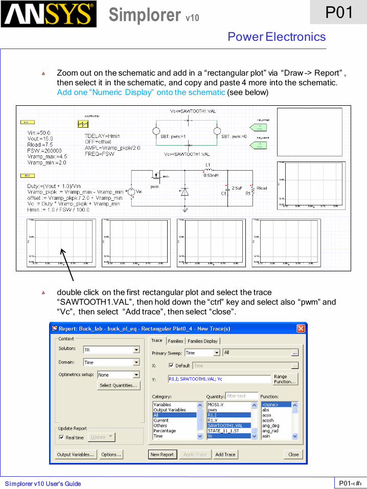
Zoom out on the schematic and add in a “rectangular plot” via “Draw -> Report” ,
then select it in the schematic, and copy and paste 4 more into the schematic.
Add one “Numeric Display” onto the schematic (see below)
double click on the first rectangular plot and select the trace
“SAWTOOTH1.VAL”, then hold down the “ctrl” key and select also “pwm” and
“Vc”, then select “Add trace”, then select “close”.
P01
Power Electronics
P01-‹#›
Simplorer v10
Simplorer v10 User’s Guide
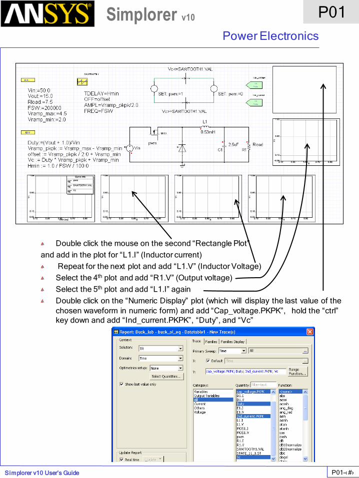
Double click the mouse on the second “Rectangle Plot”
and add in the plot for “L1.I” (Inductor current)
Repeat for the next plot and add “L1.V” (Inductor Voltage)
Select the 4th plot and add “R1.V” (Output voltage)
Select the 5th plot and add “L1.I” again
Double click on the “Numeric Display” plot (which will display the last value of the
chosen waveform in numeric form) and add “Cap_voltage.PKPK”, hold the “ctrl”
key down and add “Ind_current.PKPK”, “Duty”, and “Vc”

P01
Power Electronics
P01-‹#›
Simplorer v10
Simplorer v10 User’s Guide
Save the Design
Simulate the design by placing the mouse over “TR” (that was defined in the
“Analysis” section earlier), then using the right mouse button, bring up the menu
then select “Analyze” (see below)
The results should appear as follows:
P01
Power Electronics
P01-‹#›
Simplorer v10
Simplorer v10 User’s Guide
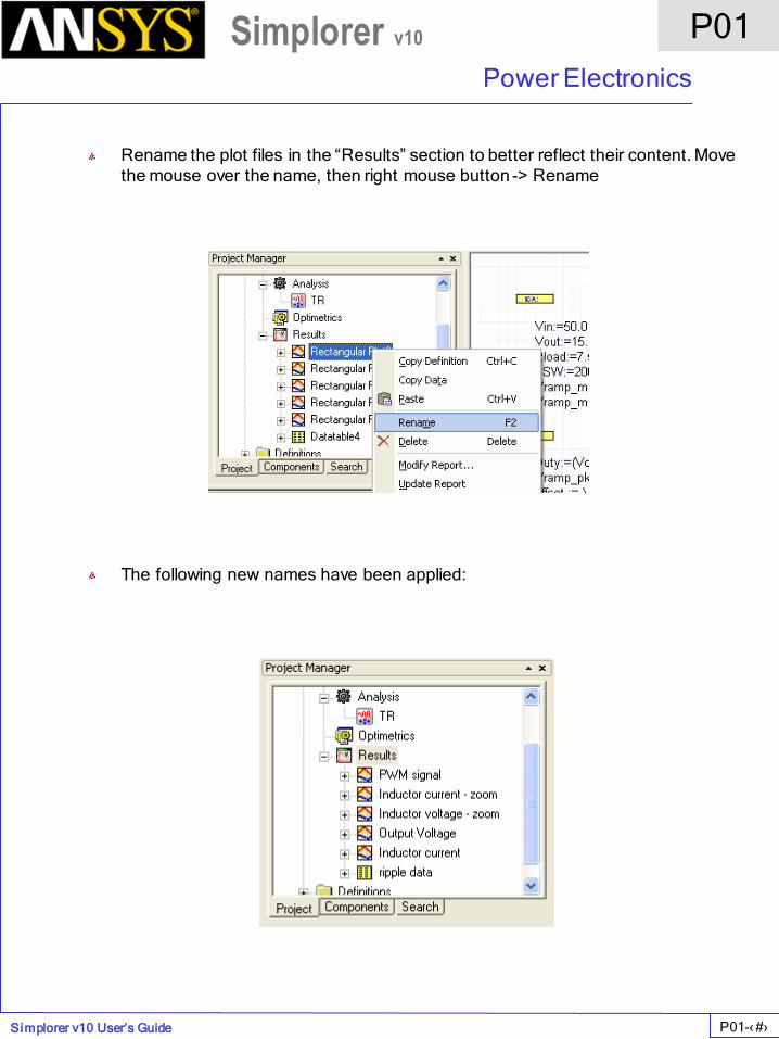
Rename the plot files in the “Results” section to better reflect their content. Move
the mouse over the name, then right mouse button -> Rename
The following new names have been applied:

P01
Power Electronics
P01-‹#›
Simplorer v10
Simplorer v10 User’s Guide
Edit the plots on the schematic to zoom the waveforms for better representation.
Select the first plot on the schematic, then use the right mouse button to bring up
the menu, then select “Edit in Place”. (Note the edit in place allows such things
as moving , re-sizing , or re-defining the legend box as well)
Move the mouse in the plot area, and again use RMB to invoke the menu, select
the “View-> Zoom In”, then draw a zoom box within the plot.
P01
Power Electronics
P01-‹#›
Simplorer v10
Simplorer v10 User’s Guide
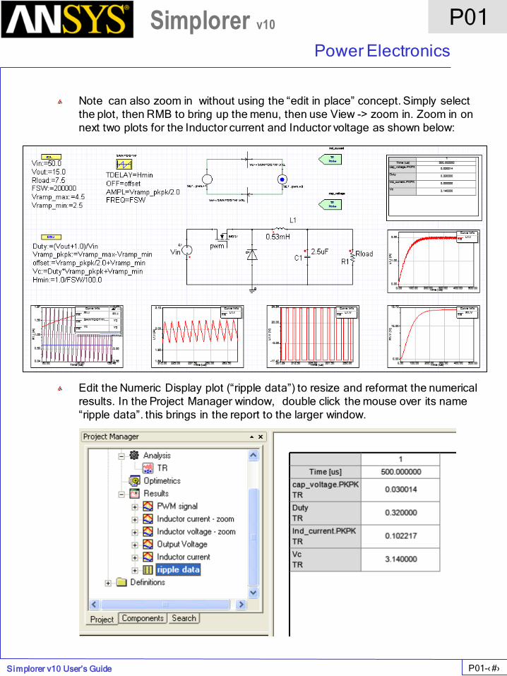
Note can also zoom in without using the “edit in place” concept. Simply select
the plot, then RMB to bring up the menu, then use View -> zoom in. Zoom in on
next two plots for the Inductor current and Inductor voltage as shown below:
Edit the Numeric Display plot (“ripple data”) to resize and reformat the numerical
results. In the Project Manager window, double click the mouse over its name
“ripple data”. this brings in the report to the larger window.
P01
Power Electronics
P01-‹#›
Simplorer v10
Simplorer v10 User’s Guide
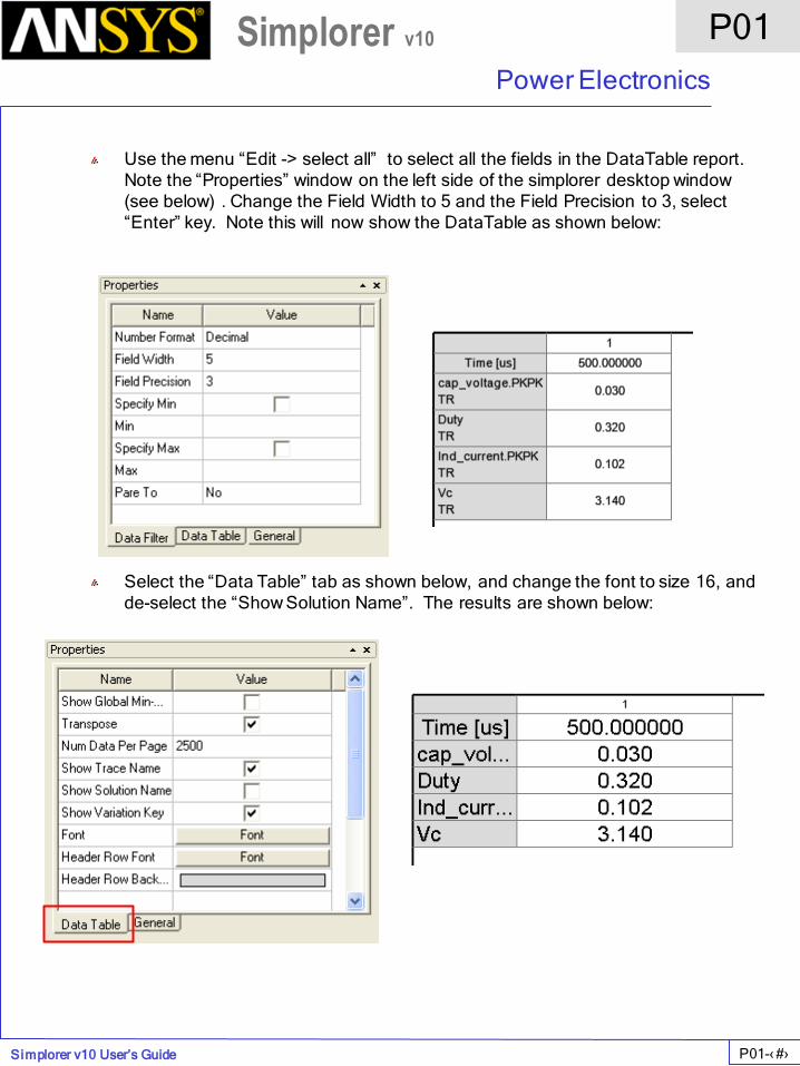
Use the menu “Edit -> select all” to select all the fields in the DataTable report.
Note the “Properties” window on the left side of the simplorer desktop window
(see below) . Change the Field Width to 5 and the Field Precision to 3, select
“Enter” key. Note this will now show the DataTable as shown below:
Select the “Data Table” tab as shown below, and change the font to size 16, and
de-select the “Show Solution Name”. The results are shown below:
P01
Power Electronics
P01-‹#›
Simplorer v10
Simplorer v10 User’s Guide
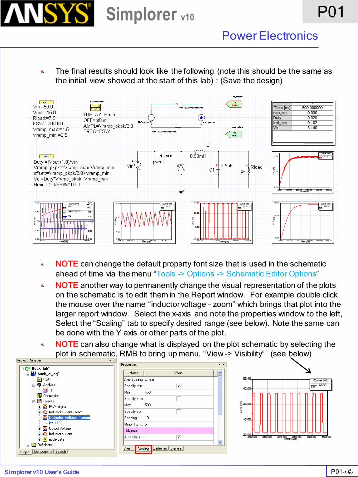
The final results should look like the following (note this should be the same as
the initial view showed at the start of this lab) : (Save the design)
NOTE can change the default property font size that is used in the schematic
ahead of time via the menu “Tools -> Options -> Schematic Editor Options”
NOTE another way to permanently change the visual representation of the plots
on the schematic is to edit them in the Report window. For example double click
the mouse over the name “inductor voltage – zoom” which brings that plot into the
larger report window. Select the x-axis and note the properties window to the left,
Select the “Scaling” tab to specify desired range (see below). Note the same can
be done with the Y axis or other parts of the plot.
NOTE can also change what is displayed on the plot schematic by selecting the
plot in schematic, RMB to bring up menu, “View -> Visibility” (see below)