annex j: serial presence detects for ddr2 sdram … · this appendix describes the serial presence...
TRANSCRIPT

Release 17
JEDEC Standard No. 21-CPage 4.1.2.10 – 1
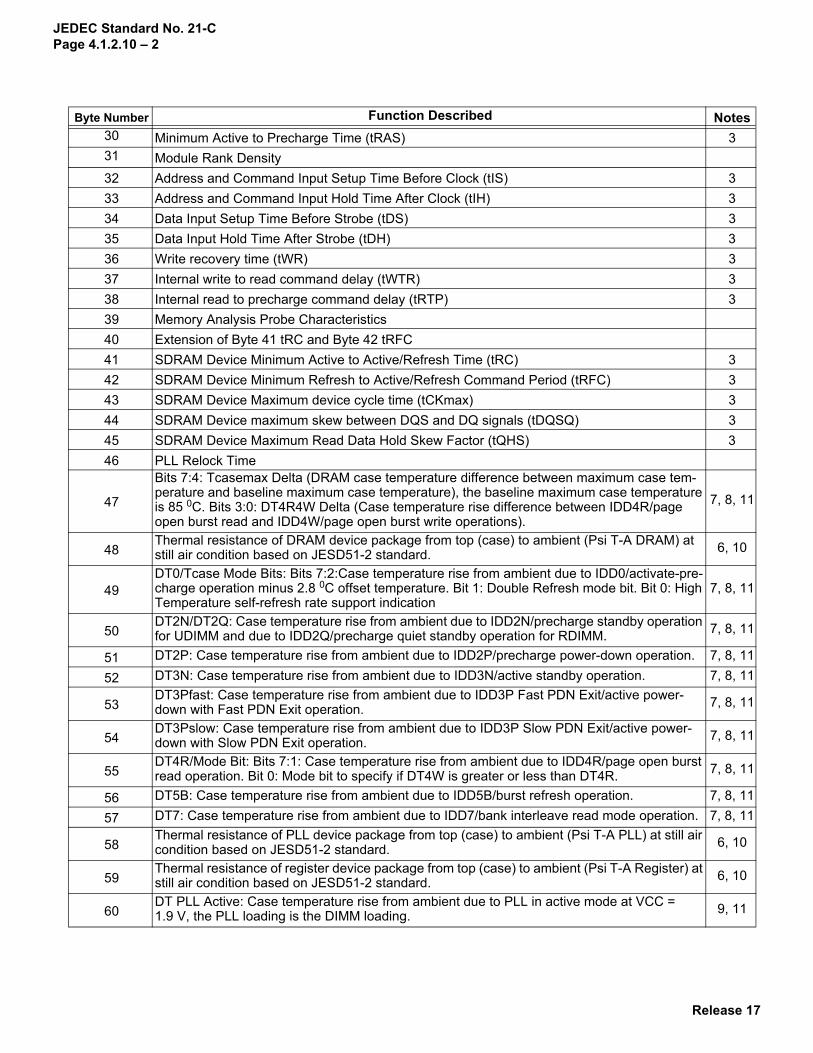
Byte Number Function Described Notes
0 Number of Serial PD Bytes written during module production 11 Total number of Bytes in Serial PD device 22 Fundamental Memory Type (FPM, EDO, SDRAM, DDR, DDR2…)3 Number of Row Addresses on this assembly4 Number of Column Addresses on this assembly5 Number of DIMM Ranks6 Data Width of this assembly7 Reserved8 Voltage Interface Level of this assembly9 SDRAM Cycle time at Maximum Supported CAS Latency (CL), CL=X 3
10 SDRAM Access from Clock11 DIMM configuration type (Non-parity, Parity or ECC)12 Refresh Rate/Type 3, 413 Primary SDRAM Width14 Error Checking SDRAM Width15 Reserved16 SDRAM Device Attributes: Burst Lengths Supported17 SDRAM Device Attributes: Number of Banks on SDRAM Device 318 SDRAM Device Attributes: CAS Latency 319 DIMM Mechanical Characteristics 320 DIMM Type Information 321 SDRAM Module Attributes22 SDRAM Device Attributes: General 323 Minimum Clock Cycle at CLX-1 324 Maximum Data Access Time (tAC) from Clock at CLX-1 325 Minimum Clock Cycle at CLX-2 326 Maximum Data Access Time (tAC) from Clock at CLX-2 327 Minimum Row Precharge Time (tRP) 328 Minimum Row Active to Row Active delay (tRRD) 329 Minimum RAS to CAS delay (tRCD) 3
Annex J: Serial Presence Detects for DDR2 SDRAM (Revision 1.3)
1.0 IntroductionThis appendix describes the serial presence detect values for the DDR2 version of the synchronous DRAM modules. These presence detect values are those referenced in the SPD standard document for ‘Specific Features’. The fol-lowing SPD fields will occur in the order presented in section 1.1. Further descriptions of Bytes 0 and 1 are found in the SPD standard. Further description of Byte 2 is found in Appendix A of the SPD standard. All unused entries will be coded as 00h. All unused bits in defined bytes will be coded as 0 except where noted. “Unused” includes reserved or TBD values.
1.1 Address mapThe following is the SPD address map for DDR2 SDRAM. It describes where the individual lookup table entries will be held in the serial EEPROM.
Release 17
JEDEC Standard No. 21-CPage 4.1.2.10 – 2
Byte Number Function Described Notes30 Minimum Active to Precharge Time (tRAS) 331 Module Rank Density32 Address and Command Input Setup Time Before Clock (tIS) 333 Address and Command Input Hold Time After Clock (tIH) 334 Data Input Setup Time Before Strobe (tDS) 335 Data Input Hold Time After Strobe (tDH) 336 Write recovery time (tWR) 337 Internal write to read command delay (tWTR) 338 Internal read to precharge command delay (tRTP) 339 Memory Analysis Probe Characteristics40 Extension of Byte 41 tRC and Byte 42 tRFC41 SDRAM Device Minimum Active to Active/Refresh Time (tRC) 342 SDRAM Device Minimum Refresh to Active/Refresh Command Period (tRFC) 343 SDRAM Device Maximum device cycle time (tCKmax) 344 SDRAM Device maximum skew between DQS and DQ signals (tDQSQ) 345 SDRAM Device Maximum Read Data Hold Skew Factor (tQHS) 346 PLL Relock Time
47
Bits 7:4: Tcasemax Delta (DRAM case temperature difference between maximum case tem-perature and baseline maximum case temperature), the baseline maximum case temperature is 85 0C. Bits 3:0: DT4R4W Delta (Case temperature rise difference between IDD4R/page open burst read and IDD4W/page open burst write operations).
7, 8, 11
48Thermal resistance of DRAM device package from top (case) to ambient (Psi T-A DRAM) at still air condition based on JESD51-2 standard. 6, 10
49DT0/Tcase Mode Bits: Bits 7:2:Case temperature rise from ambient due to IDD0/activate-pre-charge operation minus 2.8 0C offset temperature. Bit 1: Double Refresh mode bit. Bit 0: High Temperature self-refresh rate support indication
7, 8, 11
50DT2N/DT2Q: Case temperature rise from ambient due to IDD2N/precharge standby operation for UDIMM and due to IDD2Q/precharge quiet standby operation for RDIMM. 7, 8, 11
51 DT2P: Case temperature rise from ambient due to IDD2P/precharge power-down operation. 7, 8, 11
52 DT3N: Case temperature rise from ambient due to IDD3N/active standby operation. 7, 8, 11
53DT3Pfast: Case temperature rise from ambient due to IDD3P Fast PDN Exit/active power-down with Fast PDN Exit operation. 7, 8, 11
54DT3Pslow: Case temperature rise from ambient due to IDD3P Slow PDN Exit/active power-down with Slow PDN Exit operation. 7, 8, 11
55DT4R/Mode Bit: Bits 7:1: Case temperature rise from ambient due to IDD4R/page open burst read operation. Bit 0: Mode bit to specify if DT4W is greater or less than DT4R. 7, 8, 11
56 DT5B: Case temperature rise from ambient due to IDD5B/burst refresh operation. 7, 8, 11
57 DT7: Case temperature rise from ambient due to IDD7/bank interleave read mode operation. 7, 8, 11
58Thermal resistance of PLL device package from top (case) to ambient (Psi T-A PLL) at still air condition based on JESD51-2 standard. 6, 10
59Thermal resistance of register device package from top (case) to ambient (Psi T-A Register) at still air condition based on JESD51-2 standard. 6, 10
60DT PLL Active: Case temperature rise from ambient due to PLL in active mode at VCC =1.9 V, the PLL loading is the DIMM loading. 9, 11

Release 17
JEDEC Standard No. 21-CPage 4.1.2.10 – 3
Byte Number Function Described Notes
61DT Register Active/Mode Bit: Bits 7:1: Case temperature rise from ambient due to register in active mode at VCC = 1.9 V, the register loading is the RDIMM loading. Bit 0: mode bit to specify register data output toggle rate 50% or 100%.
9, 11
62 SPD Revision63 Checksum for Bytes 0-62
64-71 Manufacturer’s JEDEC ID Code72 Module Manufacturing Location 5
73-90 Module Part Number 591-92 Module Revision Code 593-94 Module Manufacturing Date95-98 Module Serial Number99-127 Manufacturer’s Specific Data 5128-255 Open for customer use
1. This will typically be programmed as 128 Bytes.2. This will typically be programmed as 256 Bytes.3. From Datasheet.4. High order bit is Self Refresh “flag”. If set to “1”, the assembly supports self refresh.5. These are optional, in accordance with the JEDEC spec.6. Refer to JESD51-3 “Low Effective Thermal Conductivity Test Board for Leaded Surface Mount Packages” under
JESD51-2 standard.7. DT parameter is derived as following: DTx = IDDx * VDD * Psi T-A, where IDDx definition is based on JEDEC
DDR2 SDRAM Component Specification and at VDD = 1.9 V, it is the datasheet (worst case) value, and Psi T-A is the programmed value of Psi T-A (value in SPD Byte 48). Programmed temperature rise data (DTx) is based on the programmed value of Psi T-A (value in SPD byte 48).
8. All DT parameters are defined for DDR2 DRAM densities up to 2 Gbit. 4 Gbit parameters will be defined later.9. DT parameters for PLL and register are derived as following: DTx = IDDx * VDD * Psi T-A, where IDDx definition
is at VDD = 1.9 V and it is the active PLL or register power corresponding to its respective DIMM configuration loading. The IDDx is the worst case value. Psi T-A used to program DTx is the programmed value of Psi T-A (value in SPD byte 58 or byte 59).
10. Rule for rounding off Psi T-A: Psi T-A shall be rounded such that it is nearest/closest to the true value of Psi T-A.11. Rule for rounding off DTx: DTx shall be rounded such that it is nearest/closest to the calculated value of DTx.

Release 17
JEDEC Standard No. 21-CPage 4.1.2.10 – 4
2.0 Details of each byte
Byte 0: Number of Bytes Utilized by Module Manufacturer
This field describes the total number of bytes used by the module manufacturer for the SPD data and any (optional) specific supplier information. The byte count includes the fields for all required and optional data.
Line # Number SPD Bytes Bit 7 Bit 6 Bit 5 Bit 4 Bit 3 Bit 2 Bit 1 Bit 0 Hex
0 Undefined 0 0 0 0 0 0 0 0 00
1 1 0 0 0 0 0 0 0 1 01
2 2 0 0 0 0 0 0 1 0 02
3 3 0 0 0 0 0 0 1 1 03
4 4 0 0 0 0 0 1 0 0 04
5 5 0 0 0 0 0 1 0 1 05
6 6 0 0 0 0 0 1 1 0 06
- - - - - - - - - - -
- - - - - - - - - - -
128 128 1 0 0 0 0 0 0 0 80
- - - - - - - - - - -
- - - - - - - - - - -
- - - - - - - - - - -
254 254 1 1 1 1 1 1 1 0 FE
255 255 1 1 1 1 1 1 1 1 FF

Release 17
JEDEC Standard No. 21-CPage 4.1.2.10 – 5
Byte 1: Total Number of Bytes in Serial PD Device
This field describes the total size of the serial memory used to hold the Serial Presence Detect data. The fol-lowing lookup table describes the possible serial memory densities (in bytes) along with the corresponding descriptor.
Byte 2: Memory Type
This byte describes the fundamental memory type (or technology) implemented on the module.
Line # Serial Memory Bit 7 Bit 6 Bit 5 Bit 4 Bit 3 Bit 2 Bit 1 Bit 0 Hex
0 Undefined 0 0 0 0 0 0 0 0 00
1 2 Bytes 0 0 0 0 0 0 0 1 01
2 4 Bytes 0 0 0 0 0 0 1 0 02
3 8 Bytes 0 0 0 0 0 0 1 1 03
4 16 Bytes 0 0 0 0 0 1 0 0 04
5 32 Bytes 0 0 0 0 0 1 0 1 05
6 64 Bytes 0 0 0 0 0 1 1 0 06
7 128 Bytes 0 0 0 0 0 1 1 1 07
8 256 Bytes 0 0 0 0 1 0 0 0 08
9 512 Bytes 0 0 0 0 1 0 0 1 09
10 1024 Bytes 0 0 0 0 1 0 1 0 0A
11 2048 Bytes 0 0 0 0 1 0 1 1 0B
12 4096 Bytes 0 0 0 0 1 1 0 0 0C
13 8192 Bytes 0 0 0 0 1 1 0 1 0D
14 16384 Bytes 0 0 0 0 1 1 1 0 0E
- - - - - - - - - - -
- - - - - - - - - - -
254 - 1 1 1 1 1 1 1 0 FE
255 - 1 1 1 1 1 1 1 1 FF
Line # Fundamental Memory Type Bit 7 Bit 6 Bit 5 Bit 4 Bit 3 Bit 2 Bit 1 Bit 0 Hex
0 Reserved 0 0 0 0 0 0 0 0 00
1 Standard FPM DRAM 0 0 0 0 0 0 0 1 01
2 EDO 0 0 0 0 0 0 1 0 02
3 Pipelined Nibble 0 0 0 0 0 0 1 1 03
4 SDRAM 0 0 0 0 0 1 0 0 04
5 ROM 0 0 0 0 0 1 0 1 05
6 DDR SGRAM 0 0 0 0 0 1 1 0 06
7 DDR SDRAM 0 0 0 0 0 1 1 1 07
8 DDR2 SDRAM 0 0 0 0 1 0 0 0 08
- - - - - - - - - - -
253 TBD 1 1 1 1 1 1 0 1 FD
254 TBD 1 1 1 1 1 1 1 0 FE
255 TBD 1 1 1 1 1 1 1 1 FF

Release 17
JEDEC Standard No. 21-CPage 4.1.2.10 – 6
Byte 3: Number of Row Addresses
This field describes the Row addressing on the module. bits 0-4 are used to represent the number of row addresses, bits 5-7 are reserved and must be coded as ‘0’.
Examples of Byte 3 implementation include:
Number of Row Addresses Module Organization Device Used Byte 3 Contents
13, RA0-RA12 32M x 64 32M x 16 0000 110114, RA0-RA13 64M x 64 64M x 8 0000 111016, RA0-RA15 512M x 64 512M x 8 0001 0000
Line # Number of RowAddresses Bit 7 Bit 6 Bit 5 Bit 4 Bit 3 Bit 2 Bit 1 Bit 0 Hex
0 Undefined 0 0 0 0 0 0 0 0 00
1 1 0 0 0 0 0 0 0 1 01
2 2 0 0 0 0 0 0 1 0 02
3 3 0 0 0 0 0 0 1 1 03
4 4 0 0 0 0 0 1 0 0 04
5 5 0 0 0 0 0 1 0 1 05
6 6 0 0 0 0 0 1 1 0 06
7 7 0 0 0 0 0 1 1 1 07
8 8 0 0 0 0 1 0 0 0 08
9 9 0 0 0 0 1 0 0 1 09
10 10 0 0 0 0 1 0 1 0 0A
11 11 0 0 0 0 1 0 1 1 0B
12 12 0 0 0 0 1 1 0 0 0C
13 13 0 0 0 0 1 1 0 1 0D
14 14 0 0 0 0 1 1 1 0 0E
15 15 0 0 0 0 1 1 1 1 0F
16 16 0 0 0 1 0 0 0 0 10
- - - - - - - - - - -
31 31 0 0 0 1 1 1 1 1 1F
32 Undefined 0 0 1 0 0 0 0 0 20
- - - - - - - - - - -
255 Undefined 1 1 1 1 1 1 1 1 FF

Release 17
JEDEC Standard No. 21-CPage 4.1.2.10 – 7
Byte 4: Number of Column Addresses
This field describes the Column addressing on the module. bit 0-3 are used to represent the number of col-umn addresses, bit 4-7 are reserved and should be coded as ‘0’
For example:
Number of Column Addresses Module Organization Device Used Byte 4 Contents
10, CA0-CA9 32M x 64 32M x 16 0000 101010, CA0-CA9 64M x 64 64M x 8 0000 1010
Line # Number of Column Addresses Bit 7 Bit 6 Bit 5 Bit 4 Bit 3 Bit 2 Bit 1 Bit 0 Hex
0 Undefined 0 0 0 0 0 0 0 0 00
1 1 0 0 0 0 0 0 0 1 01
2 2 0 0 0 0 0 0 1 0 02
3 3 0 0 0 0 0 0 1 1 03
4 4 0 0 0 0 0 1 0 0 04
5 5 0 0 0 0 0 1 0 1 05
6 6 0 0 0 0 0 1 1 0 06
7 7 0 0 0 0 0 1 1 1 07
8 8 0 0 0 0 1 0 0 0 08
9 9 0 0 0 0 1 0 0 1 09
10 10 0 0 0 0 1 0 1 0 0A
11 11 0 0 0 0 1 0 1 1 0B
12 12 0 0 0 0 1 1 0 0 0C
13 13 0 0 0 0 1 1 0 1 0D
14 14 0 0 0 0 1 1 1 0 0E
15 15 0 0 0 0 1 1 1 1 0F
- - - - - - - - - - -
254 254 1 1 1 1 1 1 1 0 FE
255 255 1 1 1 1 1 1 1 1 FF

Release 17
JEDEC Standard No. 21-CPage 4.1.2.10 – 8
Byte 5: Module Attributes - Number of Ranks, Package and Height
This field describes the number of ranks (Rank: any DRAMs connected to same physical CS) and package on the SDRAM module, and module height. The number of logical banks for the SDRAM device is defined in Byte 17.
Bit 7 ~ Bit 5 Bit 4 Bit 3 Bit 2 ~ Bit 0
Module Height DRAM Package Card on Card # of Ranks
Bit[ 7, 6, 5] 000 = less than 25.4 mm 001 = 25.4 mm 010 = greater than 25.4 mm and less than 30 mm 011 = 30.0 mm 100 = 30.5 mm 101 = greater than 30.5 mm
1 = stack0 = planar
1 = yes0 = no
Bit [2, 1, 0] : 000 = 1 rank 001 = 2 ranks 010 = 3 ranks 011 = 4 ranks ...... 111 = 8 ranks

Release 17
JEDEC Standard No. 21-CPage 4.1.2.10 – 9
Byte 6: Module Data Width
Byte 6 is used to designate the module’s data width. For example:
Byte 7: Reserved
Line # Data Width Bit 7 Bit 6 Bit 5 Bit 4 Bit 3 Bit 2 Bit 1 Bit 0 Hex
Not defined 0 0 0 0 0 0 0 0 0 00- - - - - - - - - - -
32 32 0 0 1 0 0 0 0 0 2033 33 0 0 1 0 0 0 0 1 21- - - - - - - - - - -
36 36 0 0 1 0 0 1 0 0 24- - - - - - - - - - -
64 64 0 1 0 0 0 0 0 0 40- - - - - - - - - - -
72 72 0 1 0 0 1 0 0 0 48- - - - - - - - - - -
80 80 0 1 0 1 0 0 0 0 50- - - - - - - - - - -
128 128 1 0 0 0 0 0 0 0 80- - - - - - - - - - -
144 144 1 0 0 1 0 0 0 0 90- - - - - - - - - - -
254 254 1 1 1 1 1 1 1 0 FE255 255 1 1 1 1 1 1 1 1 FF
Release 17
JEDEC Standard No. 21-CPage 4.1.2.10 – 10
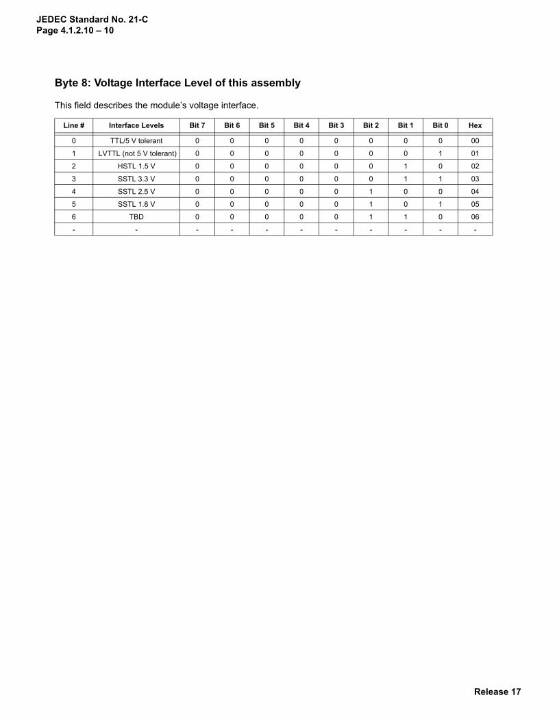
Byte 8: Voltage Interface Level of this assembly
This field describes the module’s voltage interface.
Line # Interface Levels Bit 7 Bit 6 Bit 5 Bit 4 Bit 3 Bit 2 Bit 1 Bit 0 Hex
0 TTL/5 V tolerant 0 0 0 0 0 0 0 0 00
1 LVTTL (not 5 V tolerant) 0 0 0 0 0 0 0 1 01
2 HSTL 1.5 V 0 0 0 0 0 0 1 0 02
3 SSTL 3.3 V 0 0 0 0 0 0 1 1 03
4 SSTL 2.5 V 0 0 0 0 0 1 0 0 04
5 SSTL 1.8 V 0 0 0 0 0 1 0 1 05
6 TBD 0 0 0 0 0 1 1 0 06
- - - - - - - - - - -

Release 17
JEDEC Standard No. 21-CPage 4.1.2.10 – 11
Byte 9: SDRAM Cycle Time
This byte defines the minimum cycle time for the SDRAM module at the highest CAS Latency, CAS Latency=X, defined in byte 18. If other CAS latencies are supported, then the associated minimum cycle times are not related in this version of the SPD standard. Byte 9, Cycle time for CAS Latency=X, is split into two nibbles: the higher order nibble (bits 4-7) designates the cycle time to a granularity of 1 ns; the value pre-sented by the lower order nibble (bits 0-3) has a granularity of 0.1 ns and is added to the value designated by the higher nibble. In addition, four lines of the lower order nibble are assigned to support +0.25, +0.33, +0.66 and +0.75. To indicate cycle time of 1.875 ns, 18h should be programmed. For example:
If bits 7:4 are and bits 3:0 are then the total time is:
0011 1101(3 ns) + (0.75 ns) = 3.75 ns
Byte 9, SDRAM Cycle Time, Subfield A: Whole Nanoseconds (Bits 4-7)
Line # Cycle Time Bit 7 Bit 6 Bit 5 Bit 4 Bit 3 Bit 2 Bit 1 Bit 0 Hex
0A Undefined 0 0 0 0 0_1A 1 ns 0 0 0 1 1_2A 2 ns 0 0 1 0 2_3A 3 ns 0 0 1 1 3_4A 4 ns 0 1 0 0 4_5A 5 ns 0 1 0 1 5_6A 6 ns 0 1 1 0 6_7A 7 ns 0 1 1 1 7_8A 8 ns 1 0 0 0 8_9A 9 ns 1 0 0 1 9_10A 10 ns 1 0 1 0 A_11A 11 ns 1 0 1 1 B_12A 12 ns 1 1 0 0 C_13A 13 ns 1 1 0 1 D_14A 14 ns 1 1 1 0 E_15A 15 ns 1 1 1 1 F_
- Undefined 1 1 1 1 1 1 1 1 FF
Byte 9, SDRAM Cycle Time Subfield B: Tenths of Nanoseconds (Bits 0-3)
Line # Cycle Time Bit 7 Bit 6 Bit 5 Bit 4 Bit 3 Bit 2 Bit 1 Bit 0 Hex
0B +0 ns
----
0 0 0 0 _01B +0.1 ns 0 0 0 1 _12B +0.2 ns 0 0 1 0 _23B +0.3 ns 0 0 1 1 _34B +0.4 ns 0 1 0 0 _45B +0.5 ns 0 1 0 1 _56B +0.6 ns 0 1 1 0 _67B +0.7 ns 0 1 1 1 _78B +0.8 ns 1 0 0 0 _89B +0.9 ns 1 0 0 1 _910B +0.25 ns 1 0 1 0 _A11B +0.33 ns 1 0 1 1 _B12B +0.66 ns 1 1 0 0 _C13B +0.75 ns 1 1 0 1 _D
- - - - - - - - - - -- Undefined 1 1 1 1 1 1 1 1 FF
See Subfield Table B
See Subfield Table B

Release 17
JEDEC Standard No. 21-CPage 4.1.2.10 – 12
Byte 10: SDRAM Access from Clock (tAC)
This byte defines the maximum clock to data out for the SDRAM module. This is the Clock to data out speci-fication at the highest given CAS Latency specified in byte 18 of this SPD specification. If other CAS latencies are supported, then the associated Maximum Clock Access times are not related in this version of the SPD standard. The byte is split into two nibbles: the higher order nibble (bits 4-7) designate the access time to a granularity of 0.1 ns; the value presented by the lower order nibble (bits 0-3) has the granularity of 0.01 ns and is added to the value designated by the higher nibble. For example:
if bits 7:4 are and bits 3:0 are then the total time is:
0011 0101(0.3 ns) + (0.05 ns) = 0.35 ns
Byte 10: SDRAM Access from Clock, Subfield A: Tenths of Nanoseconds (Bits 4-7)
Line # Access from Clock Bit 7 Bit 6 Bit 5 Bit 4 Bit 3 Bit 2 Bit 1 Bit 0 Hex
0A Undefined 0 0 0 0 0_1A 0.1 ns 0 0 0 1 1_2A 0.2 ns 0 0 1 0 2_3A 0.3 ns 0 0 1 1 3_4A 0.4 ns 0 1 0 0 4_5A 0.5 ns 0 1 0 1 5_6A 0.6 ns 0 1 1 0 6_7A 0.7 ns 0 1 1 1 7_8A 0.8 ns 1 0 0 0 8_9A 0.9 ns 1 0 0 1 9_10A RFU 1 0 1 0 A_11A - 1 0 1 1 -
- Undefined 1 1 1 1 1 1 1 1 FF
Byte 10: SDRAM Access from Clock Subfield B: Hundredths of Nanoseconds (Bits 0-3)
Line # Access from Clock Bit 7 Bit 6 Bit 5 Bit 4 Bit 3 Bit 2 Bit 1 Bit 0 Hex
0B +0 ns 0 0 0 0 _01B +0.01 ns 0 0 0 1 _12B +0.02 ns 0 0 1 0 _23B +0.03 ns 0 0 1 1 _34B +0.04 ns 0 1 0 0 _45B +0.05 ns 0 1 0 1 _56B +0.06 ns 0 1 1 0 _67B +0.07 ns 0 1 1 1 _78B +0.08 ns 1 0 0 0 _89B +0.09 ns 1 0 0 1 _910B RFU 1 0 1 0 _A11B – - - - - - - - - -
- Undefined 1 1 1 1 1 1 1 1 FF
See Subfield B
See Subfield A

Release 17
JEDEC Standard No. 21-CPage 4.1.2.10 – 13
Byte 11: DIMM Configuration Type
This byte describes the module’s error detection and/or correction schemes on the data, address and com-mand buses.
Byte 12: Refresh Rate
This byte describes the module’s refresh rate in microseconds.
Bit 7 Bit 6 Bit 5 Bit 4 Bit 3 Bit 2 Bit 1 Bit 0
TBD TBD TBD TBD TBD Address/Command Parity Data ECC Data Parity
0 0 0 0 0 1 or 0 1 or 0 1 or 0
1 = Supported on this assembly, 0 = Not supported on this assembly.Note: Data ECC includes Data Parity, therefore modules with Data ECC shall encode bit 1 as 1 and bit 0 as 0.
Line # Refresh Period Bit 7 Bit 6 Bit 5 Bit 4 Bit 3 Bit 2 Bit 1 Bit 0 Hex
0 Normal (15.625 μs) 1 0 0 0 0 0 0 0 80
1 Reduced (.25x)...3.9 μs 1 0 0 0 0 0 0 1 81
2 Reduced (.5x)...7.8 μs 1 0 0 0 0 0 1 0 82
3 Extended (2x)...31.3 μs 1 0 0 0 0 0 1 1 83
4 Extended (4x)...62.5 μs 1 0 0 0 0 1 0 0 84
5 Extended (8x)...125 μs 1 0 0 0 0 1 0 1 85
6 TBD 1 0 0 0 0 1 1 0 86
7 TBD 1 0 0 0 0 1 1 1 87
- - - - - - - - - - -
- - - - - - - - - - -

Release 17
JEDEC Standard No. 21-CPage 4.1.2.10 – 14
Byte 13: Primary SDRAM Width
Bits 0-7 of this byte indicate the width of the primary data SDRAM. The primary SDRAM is that which is used for data; examples of primary (data) SDRAM widths are x4, x8, x16, and x32. Note that if the module is made with SDRAMs which provide for data and error checking, e.g. x9, x18, and x36, then it is also designated in this field.
This table contains examples of SDRAM DIMM Module Width
Primary SDRAM Width
Error Checking SDRAM Width
Byte 13 Contents
x72 x8 x8 0000 1000x72 x16 x16 0001 0000
Line # SDRAM Data Width Bit 7 Bit 6 Bit 5 Bit 4 Bit 3 Bit 2 Bit 1 Bit 0 Hex
0 Undefined 0 0 0 0 0 0 0 0 00
1 1 0 0 0 0 0 0 0 1 01
2 2 0 0 0 0 0 0 1 0 02
3 3 0 0 0 0 0 0 1 1 03
4 4 0 0 0 0 0 1 0 0 04
5 5 0 0 0 0 0 1 0 1 05
6 6 0 0 0 0 0 1 1 0 06
7 7 0 0 0 0 0 1 1 1 07
8 8 0 0 0 0 1 0 0 0 08
9 9 0 0 0 0 1 0 0 1 09
10 10 0 0 0 0 1 0 1 0 0A
11 11 0 0 0 0 1 0 1 1 0B
12 12 0 0 0 0 1 1 0 0 0C
13 13 0 0 0 0 1 1 0 1 0D
14 14 0 0 0 0 1 1 1 0 0E
15 15 0 0 0 0 1 1 1 1 0F
- - - - - - - - - - -
254 254 1 1 1 1 1 1 1 0 FE
255 255 1 1 1 1 1 1 1 1 FF

Release 17
JEDEC Standard No. 21-CPage 4.1.2.10 – 15
Byte 14: Error Checking SDRAM Width
If the module incorporates error checking and if the primary data SDRAM does not include these bits — i.e. there are separate error checking SDRAMs — then the error checking SDRAM’s width is expressed in this byte. Bits 0-7 of this byte relate the error checking SDRAM’s width.
The following table contains examples of error checking SDRAM widths
Module Width
Primary SDRAM Width
Error Checking SDRAM Width
Possible (512Mb based) Module
Density
Byte 14 Contents
x72 x8 x8 512 MB 0000 1000x72 x16 x16 256 MB 0001 0000
Line # Error CheckingSDRAM Width Bit 7 Bit 6 Bit 5 Bit 4 Bit 3 Bit 2 Bit 1 Bit 0 Hex
0 Undefined 0 0 0 0 0 0 0 0 00
1 1 0 0 0 0 0 0 0 1 01
2 2 0 0 0 0 0 0 1 0 02
3 3 0 0 0 0 0 0 1 1 03
4 4 0 0 0 0 0 1 0 0 04
5 5 0 0 0 0 0 1 0 1 05
6 6 0 0 0 0 0 1 1 0 06
7 7 0 0 0 0 0 1 1 1 07
8 8 0 0 0 0 1 0 0 0 08
9 9 0 0 0 0 1 0 0 1 09
10 10 0 0 0 0 1 0 1 0 0A
11 11 0 0 0 0 1 0 1 1 0B
12 12 0 0 0 0 1 1 0 0 0C
13 13 0 0 0 0 1 1 0 1 0D
14 14 0 0 0 0 1 1 1 0 0E
15 15 0 0 0 0 1 1 1 1 0F
- - - - - - - - - - -
254 254 1 1 1 1 1 1 1 0 FE
255 255 1 1 1 1 1 1 1 1 FF

Release 17
JEDEC Standard No. 21-CPage 4.1.2.10 – 16
Byte 15: Reserved
Byte 16: SDRAM Device Attributes – Burst Lengths Supported
This byte describes which various programmable burst lengths are supported by the devices on the module. If the bit is “1”, then that Burst Length is supported on the module; if the bit is “0”, then that Burst Length is not supported by the module.
Byte 17: SDRAM Device Attributes – Number of Banks on SDRAM Device
This byte details how many banks are on each SDRAM installed onto the module.
Byte 18: SDRAM Device Attributes – CAS Latency
This byte describes which of the programmable CAS latencies are acceptable for the module. If the bit is “1”, then that CAS latency is supported on the module; if the bit is “0”, then that CAS latency is not supported by the module.
Bit 7 Bit 6 Bit 5 Bit 4 Bit 3 Bit 2 Bit 1 Bit 0
TBD TBD TBD TBD Burst Length= 8
Burst Length= 4 TBD TBD
0 0 0 0 1 or 0 1 or 0 0 0
1 = Supported on this assembly, 0 = Not supported on this assembly.
Line # Number of Banks Bit 7 Bit 6 Bit 5 Bit 4 Bit 3 Bit 2 Bit 1 Bit 0 Hex
0 Undefined 0 0 0 0 0 0 0 0 00
- - - - - - - - - - -
- - - - - - - - - - -
4 4 0 0 0 0 0 1 0 0 04
- - - - - - - - - - -
8 8 0 0 0 0 1 0 0 0 08
- - - - - - - - - - -
255 255 1 1 1 1 1 1 1 1 FF
Bit 7 Bit 6 Bit 5 Bit 4 Bit 3 Bit 2 Bit 1 Bit 0
CAS Latency= 7
CAS Latency= 6
CAS Latency= 5
CAS Latency = 4
CAS Latency= 3
CAS Latency= 2 TBD TBD
1 or 0 1 or 0 1 or 0 1 or 0 1 or 0 1 or 0 0 0
1 = Supported on this assembly; 0 = Not supported on this assembly.

Release 17
JEDEC Standard No. 21-CPage 4.1.2.10 – 17
Byte 19: DIMM Mechanical Characteristics
This byte identifies the DDR2 SDRAM memory module mechanical information. Each memory module type as specified in Byte 20 defines a unique encoding of thickness ranges in Byte 19. Module thickness is the maximum value including all finished assembly parts: devices, heat spreaders, or other mechanical components.
Decoding of the module thickness field, based on module type:
TypeReserved Module Thickness
Bit 7 Bit 6 Bit 5 Bit 4 Bit 3 Bit 2 Bit 1 Bit 0Undefined / Not Specified
Reserved0 0 0
Thickness (See Indexed Tables below) x x x
Module Thickness RDIMM UDIMM SO-DIMM Micro-DIMM Mini-RDIMM Mini-UDIMMUnit
Bit 2 Bit 1 Bit 0 Byte 20= 01 hex
Byte 20= 02 hex
Byte 20= 04 hex
Byte 20= 08 hex
Byte 20= 10 hex
Byte 20= 20 hex
0 0 0 Undefined / Not specified mm
0 0 1 x ≤ 4.10 x ≤ 4.10 x ≤ 3.80 x ≤ 3.80 x ≤ 3.85 x ≤ 3.85 mm
0 1 0 4.10 < x ≤ 6.75 4.10 < x ≤ 6.75 3.80 < x ≤ TBD 3.80 < x ≤ TBD 3.85 < x ≤ 6.45 3.85 < x ≤ 6.45 mm
0 1 1 6.75 < x ≤ 7.55 6.75 < x ≤ 7.55 TBD < x ≤ TBD TBD < x ≤ TBD 6.45 < x ≤ 7.25 6.45 < x ≤ 7.25 mm
1 0 0 7.55 < x 7.55 < x TBD < x TBD < x 7.25 < x 7.25 < x mm
1 0 1 Reserved Reserved Reserved Reserved Reserved Reserved mm1 1 0 Reserved Reserved Reserved Reserved Reserved Reserved mm1 1 1 Reserved Reserved Reserved Reserved Reserved Reserved mm
Module Thickness 72b-SO-RDIMM 72b-SO-CDIMMUnit
Bit 2 Bit 1 Bit 0 Byte 20= 07 hex
Byte 20= 06 hex
0 0 0 Undefined / Not specified mm
0 0 1 x ≤ 3.80 x ≤ 3.80 mm
0 1 0 3.80 < x ≤ 7.10 3.80 < x ≤ 7.10 mm
0 1 1 7.10 < x 7.10 < x mm
1 0 0 Reserved Reserved mm1 0 1 Reserved Reserved mm1 1 0 Reserved Reserved mm1 1 1 Reserved Reserved mm

Release 17
JEDEC Standard No. 21-CPage 4.1.2.10 – 18Byte 20: DIMM type information
This byte identifies the DDR2 SDRAM memory module type. Each module type specified in Byte 20 defines a unique index for module thicknesses specified in Byte 19, which may be used in conjunction with thermal specifications in Bytes 21 and 47 - 61 to adjust system operating conditions based on installed modules.
TypeReserved Module Type
HexBit 7 Bit 6 Bit 5 Bit 4 Bit 3 Bit 2 Bit 1 Bit 0
Undefined / Not specified
Reserved
0 0 0 0 0 0 00RDIMM
(width = 133.35 mm nom) 0 0 0 0 0 1 01
UDIMM(width = 1333.35 mm nom) 0 0 0 0 1 0 02
SO-DIMM(width = 67.60 mm nom) 0 0 0 1 0 0 04
72b-SO-CDIMM(width = 67.60 mm nom) 0 0 0 1 1 0 06
72b-SO-RDIMM(width = 67.60 mm nom) 0 0 0 1 1 1 07
Micro-DIMM(width = 54.00 mm nom) 0 0 1 0 0 0 08
Mini-RDIMM(width = 82.00 mm nom) 0 1 0 0 0 0 10
Mini-UDIMM(width = 82.00 mm nom) 1 0 0 0 0 0 20
Reserved All other encodings of bits 0:5
Definitions: RDIMM: Registered Dual In-Line Memory Module UDIMM: Unbuffered Dual In-Line Memory Module SO-DIMM: Small Outline Dual In-Line Memory Module 72b-SO-CDIMM: Clocked SO-DIMM with 72-bit data bus 72b-SO-RDIMM: Registered SO-DIMM with 72-bit data bus Micro-DIMM: Micro Dual In-Line Memory Module Mini-RDIMM: Mini Registered Dual In-Line Memory Module Mini-UDIMM: Mini Unbuffered Dual In-Line Memory Module

Release 17
JEDEC Standard No. 21-CPage 4.1.2.10 – 19
Byte 21: SDRAM Modules Attributes
This byte depicts various aspects of the module. It details various unrelated but critical elements pertinent to the module. A given module characteristic is detailed in the designated bit. Bit 1:0 defines the number of active regis-ters on the DIMM, the active register is defined as being in active mode with clock running within spec and OE enabled. If two registers do not have a common select S inputs, only one is considered active. Bit 3:2 defines the number of PLLs on the DIMM. Please refer to Byte 20 for DIMM type information.
Byte 22: SDRAM Device Attributes – General
This byte depicts various aspects of the SDRAMs on the module. It details various unrelated but critical elements pertinent to the SDRAMs. A given SDRAM characteristic is detailed in the designated bit; if the aspect is TRUE, then the bit is “1”. Conversely, if the aspect is FALSE, the designated bit is “0”.
Bit 7 Bit 6 Bit 5 Bit 4 Bit [3:2] Bit [1:0]
TBD Analysis probe installed* TBD
FET Switch External Enable
Number of PLLs on the DIMM
Number of Active Registers on the DIMM**
0 1 or 0 0 1 or 0
00 : 001 : 110 : 2
11 : Reserved for future use
00 : 101 : 210 : 311 : 4
1 = Included on this assembly; 0 = Not included on this assembly.* All normal DIMMs will set bit 6 to 0. If bit 6 is set to a 1 this indicates that a memory bus analysis probe is installed in the slot. The BIOS should ensure that Address and Command bus clocks remain turned for that slot and byte 39 may be optionally consulted to determine probe characteristics** Bits 1:0 are only applicable if Byte 20 [Bit0 or Bit4] are set to 1. If Byte 20 [Bit0 and Bit4] are both set to 0, then Byte 21 Bit[1:0] are “don’t care”, and recommended content in this case is “00”.
Bit 7 Bit 6 Bit 5 Bit 4 Bit 3 Bit 2 Bit 1 Bit 0
TBD TBD TBD TBD TBD Supports PASR(Partial Array Self Refresh)
Supports 50 ohm ODT
SupportsWeak Driver
0 0 0 0 0 1 or 0 1 or 0 1 or 0

Release 17
JEDEC Standard No. 21-CPage 4.1.2.10 – 20
Byte 23: Minimum Clock Cycle Time at Reduced CAS Latency, X- 1
The highest CAS latency identified in byte 18 is X and the timing values associated with CAS latency ‘X’ are found at byte locations 9 and 10. Byte 23 denotes the minimum cycle time at CAS latency X- 1.
For example, if byte 18 denotes CAS latencies of 3 to 4, then X is 4 and X-1 is 3. Byte 23 then denotes the minimum cycle time at CAS latency 3.
Byte 23 is split into two nibbles: the higher order nibble (bits 4-7) designate the cycle time to a granularity of 1ns; the value presented by the lower order nibble (bits 0-3) has a granularity of 0.1 ns and is added to the value designated by the higher nibble. In addition, four lines of the lower order nibble are assigned to support +0.25, +0.33, +0.66 and +0.75. To indicate cycle time of 1.875 ns, 18h should be programmed. For example:
if bits 7:4 are and bits 3:0 are then the total time is
0011 1101(3 ns) + (0.75 ns) =3.75 ns
Byte 23, SDRAM Minimum Cycle Time @ CL X-1, Subfield A: Whole Nanoseconds (Bits 4-7)
Line # Access from Clock Bit 7 Bit 6 Bit 5 Bit 4 Bit 3 Bit 2 Bit 1 Bit 0 Hex
0A Undefined 0 0 0 0 0_1A 1 ns/16 ns 0 0 0 1 1_2A 2 ns/17 ns 0 0 1 0 2_3A 3 ns 0 0 1 1 3_4A 4 ns 0 1 0 0 4_5A 5 ns 0 1 0 1 5_6A 6 ns 0 1 1 0 6_7A 7 ns 0 1 1 1 7_8A 8 ns 1 0 0 0 8_9A 9 ns 1 0 0 1 9_10A 10 ns 1 0 1 0 A_11A 11 ns 1 0 1 1 B_12A 12 ns 1 1 0 0 C_13A 13 ns 1 1 0 1 D_14A 14 ns 1 1 1 0 E_15A 15 ns 1 1 1 1 F_
Byte 23, SDRAM Minimum Cycle Time @ CL X-1, Subfield B: Tenths of Nanoseconds (Bits 0-3)
Line # Access from Clock Bit 7 Bit 6 Bit 5 Bit 4 Bit 3 Bit 2 Bit 1 Bit 0 Hex
0B +0 ns 0 0 0 0 _01B +0.1 ns 0 0 0 1 _12B +0.2 ns 0 0 1 0 _23B +0.3 ns 0 0 1 1 _34B +0.4 ns 0 1 0 0 _45B +0.5 ns 0 1 0 1 _56B +0.6 ns 0 1 1 0 _67B +0.7 ns 0 1 1 1 _78B +0.8 ns 1 0 0 0 _89B +0.9 ns 1 0 0 1 _910B +0.25 ns 1 0 1 0 _A11B +0.33 ns 1 0 1 1 _B12B +0.66 ns 1 1 0 0 _C13B +0.75 ns 1 1 0 1 _D
- . . . . . . . . . .- Undefined 1 1 1 1 1 1 1 1 FF
See Subfield B
See Subfield A

Release 17
JEDEC Standard No. 21-CPage 4.1.2.10 – 21
Byte 24: Maximum Data Access Time (tAC) from Clock at CL X- 1
The highest CAS latency identified in byte 18 is X. Byte 23 denotes the maximum access time from Clock at CAS latency X- 1.
For example, if byte 18 denotes supported CAS latencies of 3 to 4, then X is 4 and X-1 is 3. Byte 24 then denotes the maximum clock access time from CK at CAS latency 3.
Byte 24 is split into two nibbles: the higher order nibble (bits 4-7) designate the access time to a granularity of 0.1ns; the value presented by the lower order nibble (bits 0-3) has the granularity of 0.01 ns and is added to the value designated by the higher nibble. For example:
if bits 7:4 are and bits 3:0 are then the total time is:
0011 0101(0.3 ns) + (0.05 ns) = 0.35 ns
Byte 24: SDRAM Access from Clock @ X-1, Subfield A: Tenths of Nanoseconds (Bits 4-7)
Line # Access from Clock Bit 7 Bit 6 Bit 5 Bit 4 Bit 3 Bit 2 Bit 1 Bit 0 Hex
0A Undefined 0 0 0 0 0_1A 0.1 ns 0 0 0 1 1_2A 0.2 ns 0 0 1 0 2_3A 0.3 ns 0 0 1 1 3_4A 0.4 ns 0 1 0 0 4_5A 0.5 ns 0 1 0 1 5_6A 0.6 ns 0 1 1 0 6_7A 0.7 ns 0 1 1 1 7_8A 0.8 ns 1 0 0 0 8_9A 0.9 ns 1 0 0 1 9_10A RFU 1 0 1 0 A_11A - 1 0 1 1 -
- Undefined 1 1 1 1 1 1 1 1 FF
Byte 24: SDRAM Access from Clock @ X-1, Subfield B: Hundredths of Nanoseconds (Bits 0-3)
Line # Access from Clock Bit 7 Bit 6 Bit 5 Bit 4 Bit 3 Bit 2 Bit 1 Bit 0 Hex
0B +0 ns 0 0 0 0 _01B +0.01 ns 0 0 0 1 _12B +0.02 ns 0 0 1 0 _23B +0.03 ns 0 0 1 1 _34B +0.04 ns 0 1 0 0 _45B +0.05 ns 0 1 0 1 _56B +0.06 ns 0 1 1 0 _67B +0.07 ns 0 1 1 1 _78B +0.08 ns 1 0 0 0 _89B +0.09 ns 1 0 0 1 _910B RFU 1 0 1 0 _A11B – - - - - - - - - -
- Undefined 1 1 1 1 1 1 1 1 FF
See Subfield B
See Subfield A

Release 17
JEDEC Standard No. 21-CPage 4.1.2.10 – 22
Byte 25: Minimum Clock Cycle Time at CL X-2
The highest CAS latency identified in byte 18 is X. Byte 25 denotes the minimum cycle time at CAS latency X-2.
For example, if byte 18 denotes CAS latencies of 3 to 5, then X is 5 and X-2 is 3. Byte 25 then denotes the minimum cycle time at CAS latency 3.
Byte 25 is split into two nibbles: the higher order nibble (bits 4-7) designates the cycle time to a granularity of 1ns; the value presented by the lower order nibble (bits 0-3) has a granularity of 0.1 ns and is added to the value designated by the higher order nibble. In addition, four lines of the lower order nibble are assigned to support +0.25, +0.33, +0.66 and +0.75. To indicate cycle time of 1.875 ns, 18h should be programmed. For example:
if bits 7:4 are and bits 3:0 are then the total time is
0011 1101(3 ns) + (0.75 ns) = 3.75 ns
Byte 25, SDRAM Minimum Cycle Time @ CL X-2, Subfield A: Whole Nanoseconds (Bits 4-7)
Line # Access from Clock Bit 7 Bit 6 Bit 5 Bit 4 Bit 3 Bit 2 Bit 1 Bit 0 Hex
0A Undefined 0 0 0 0 0_1A 1 ns/16 ns 0 0 0 1 1_2A 2 ns/17 ns 0 0 1 0 2_3A 3 ns 0 0 1 1 3_4A 4 ns 0 1 0 0 4_5A 5 ns 0 1 0 1 5_6A 6 ns 0 1 1 0 6_7A 7 ns 0 1 1 1 7_8A 8 ns 1 0 0 0 8_9A 9 ns 1 0 0 1 9_10A 10 ns 1 0 1 0 A_11A 11 ns 1 0 1 1 B_12A 12 ns 1 1 0 0 C_13A 13 ns 1 1 0 1 D_14A 14 ns 1 1 1 0 E_15A 15 ns 1 1 1 1 F_
Byte 25, SDRAM Minimum Cycle Time @ CL X-2, Subfield B: Tenths of Nanoseconds (Bits 0-3)
Line # Access from Clock Bit 7 Bit 6 Bit 5 Bit 4 Bit 3 Bit 2 Bit 1 Bit 0 Hex
0B +0 ns 0 0 0 0 _01B +0.1 ns 0 0 0 1 _12B +0.2 ns 0 0 1 0 _23B +0.3 ns 0 0 1 1 _34B +0.4 ns 0 1 0 0 _45B +0.5 ns 0 1 0 1 _56B +0.6 ns 0 1 1 0 _67B +0.7 ns 0 1 1 1 _78B +0.8 ns 1 0 0 0 _89B +0.9 ns 1 0 0 1 _910B +0.25 ns 1 0 1 0 _A11B +0.33 ns 1 0 1 1 _B12B +0.66 ns 1 1 0 0 _C13B +0.75 ns 1 1 0 1 _D
- . . . . . . . . . .- Undefined 1 1 1 1 1 1 1 1 FF
See Subfield B
See Subfield A

Release 17
JEDEC Standard No. 21-CPage 4.1.2.10 – 23
Byte 26: Maximum Data Access Time (tAC) from Clock at CL X-2
The highest CAS latency identified in byte 18 is X. Byte 26 denotes the maximum access time from Clock at CAS latency X-2.
For example, if byte 18 denotes supported CAS latencies of 3 to 5, then X is 5 and X-2 is 3. Byte 26 then denotes the maximum data access time from CK at CAS latency 3.
Byte 26 is split into two nibbles: the higher order nibble (bits 4-7) designate the access time to a granularity of 0.1 ns; the value presented by the lower order nibble (bits 0-3) has the granularity of 0.01 ns and is added to the value designated by the higher nibble. For example:
if bits 7:4 are and bits 3:0 are then the total time is:
0011 0101(0.3 ns) + (0.05 ns) = 0.35 ns
Byte 26: SDRAM Access from Clock @ CL = X-2, Subfield A: Tenths of Nanoseconds (Bits 4-7)
Line # Access from Clock Bit 7 Bit 6 Bit 5 Bit 4 Bit 3 Bit 2 Bit 1 Bit 0 Hex
0A Undefined 0 0 0 0 0_1A 0.1 ns 0 0 0 1 1_2A 0.2 ns 0 0 1 0 2_3A 0.3 ns 0 0 1 1 3_4A 0.4 ns 0 1 0 0 4_5A 0.5 ns 0 1 0 1 5_6A 0.6 ns 0 1 1 0 6_7A 0.7 ns 0 1 1 1 7_8A 0.8 ns 1 0 0 0 8_9A 0.9 ns 1 0 0 1 9_10A RFU 1 0 1 0 A_11A - 1 0 1 1 -
- Undefined 1 1 1 1 1 1 1 1 FF
Byte 26: SDRAM Access from Clock @ CL = X-2, Subfield B: Hundredths of Nanoseconds (Bits 0-3)
Line # Access from Clock Bit 7 Bit 6 Bit 5 Bit 4 Bit 3 Bit 2 Bit 1 Bit 0 Hex
0B +0 ns 0 0 0 0 _01B +0.01 ns 0 0 0 1 _12B +0.02 ns 0 0 1 0 _23B +0.03 ns 0 0 1 1 _34B +0.04 ns 0 1 0 0 _45B +0.05 ns 0 1 0 1 _56B +0.06 ns 0 1 1 0 _67B +0.07 ns 0 1 1 1 _78B +0.08 ns 1 0 0 0 _89B +0.09 ns 1 0 0 1 _910B RFU 1 0 1 0 _A11B – - - - - - - - - -
- Undefined 1 1 1 1 1 1 1 1 FF
See Subfield B
See Subfield A

Release 17
JEDEC Standard No. 21-CPage 4.1.2.10 – 24
Byte 27: Minimum Row Precharge Time (tRP)
Byte 27 is used to designate the module’s minimum Row Precharge time.
Byte 27 is split into two pieces: the higher order bits (bits 2-7) designate the time to a granularity of 1 ns; the value presented by the lower order bits (bits 0-1) has a granularity of 0.25 ns and is added to the value desig-nated by the higher bits. To indicate 13.125 ns time for DDR2-1066 7-7-7 speed bin, it should be pro-grammed as 34h. For example:
if bits 7:2 are and bits 1:0 are then the total time is
001111(15 ns)
00+(0.0 ns) = 15.0 ns
010010(18 ns)
11+(0.75 ns) = 18.75 ns
Byte 27, SDRAM Minimum tRP Time, Subfield A: Whole Nanoseconds (Bits 2-7)
Nanoseconds Bit 7 Bit 6 Bit 5 Bit 4 Bit 3 Bit 2 Bit 1 Bit 0
Undefined 0 0 0 0 0 0
1 ns 0 0 0 0 0 1
2 ns 0 0 0 0 1 0
3 ns 0 0 0 0 1 1
4 ns 0 0 0 1 0 0
5 ns 0 0 0 1 0 1
6 ns 0 0 0 1 1 0
7 ns 0 0 0 1 1 1
8 ns 0 0 1 0 0 0
9 ns 0 0 1 0 0 1
10 ns 0 0 1 0 1 0
: : : : : : :
: : : : : : :
61 ns 1 1 1 1 0 1
62 ns 1 1 1 1 1 0
63 ns 1 1 1 1 1 1
Byte 27, SDRAM Minimum tRP Time, Subfield B: Quarters of Nanoseconds (Bits 0-1)
Access from Clock Bit 7 Bit 6 Bit 5 Bit 4 Bit 3 Bit 2 Bit 1 Bit 0
+0 ns 0 0
+0.25 ns 0 1
+0.50 ns 1 0
+0.75 ns 1 1
See Subfield B
See Subfield A

Release 17
JEDEC Standard No. 21-CPage 4.1.2.10 – 25
Byte 28: Minimum Row Active to Row Active Delay (tRRD)
This field describes the minimum required delay between different row activations.
Byte 28 is split into two pieces: the higher order bits (bits 2-7) designate the time to a granularity of 1 ns; the value presented by the lower order bits (bits 0-1) has a granularity of 0.25 ns and is added to the value desig-nated by the higher bits. For example:
if bits 7:2 are and bits 1:0 are then the total time is
000111(7 ns)
10+(0.5 ns) = 7.5 ns
001010(10 ns)
00+(0.0 ns) = 10 ns
Byte 28, SDRAM Minimum tRRD Time, Subfield A: Whole Nanoseconds (Bits 2-7)
Nanoseconds Bit 7 Bit 6 Bit 5 Bit 4 Bit 3 Bit 2 Bit 1 Bit 0
Undefined 0 0 0 0 0 0
1 ns 0 0 0 0 0 1
2 ns 0 0 0 0 1 0
3 ns 0 0 0 0 1 1
4 ns 0 0 0 1 0 0
5 ns 0 0 0 1 0 1
6 ns 0 0 0 1 1 0
7 ns 0 0 0 1 1 1
8 ns 0 0 1 0 0 0
9 ns 0 0 1 0 0 1
10 ns 0 0 1 0 1 0
: : : : : : :
: : : : : : :
61 ns 1 1 1 1 0 1
62 ns 1 1 1 1 1 0
63 ns 1 1 1 1 1 1
Byte 28, SDRAM Minimum tRRD Time, Subfield B: Quarters of Nanoseconds (Bits 0-1)
Access from Clock Bit 7 Bit 6 Bit 5 Bit 4 Bit 3 Bit 2 Bit 1 Bit 0
+0 ns 0 0
+0.25 ns 0 1
+0.50 ns 1 0
+0.75 ns 1 1
See Subfield B
See Subfield A

Release 17
JEDEC Standard No. 21-CPage 4.1.2.10 – 26
Byte 29: Minimum RAS to CAS Delay (tRCD)
This byte describes the minimum delay required between assertions of RAS and CAS to the same bank.
Byte 29 is split into two pieces: the higher order bits (bits 2-7) designate the time to a granularity of 1 ns; the value presented by the lower order bits (bits 0-1) has a granularity of 0.25 ns and is added to the value desig-nated by the higher bits. To indicate 13.125 ns time for DDR2-1066 7-7-7 speed bin, it should be programmed as 34h. For example:
if bits 7:2 are and bits 1:0 are then the total time is
001111(15 ns)
00+(0.0 ns) = 15.0 ns
010010(18 ns)
11+(0.75 ns) = 18.75 ns
Byte 29, SDRAM Minimum tRCD Time, Subfield A: Whole Nanoseconds (Bits 2-7)
Nanoseconds Bit 7 Bit 6 Bit 5 Bit 4 Bit 3 Bit 2 Bit 1 Bit 0
Undefined 0 0 0 0 0 0
1 ns 0 0 0 0 0 1
2 ns 0 0 0 0 1 0
3 ns 0 0 0 0 1 1
4 ns 0 0 0 1 0 0
5 ns 0 0 0 1 0 1
6 ns 0 0 0 1 1 0
7 ns 0 0 0 1 1 1
8 ns 0 0 1 0 0 0
9 ns 0 0 1 0 0 1
10 ns 0 0 1 0 1 0
: : : : : : :
: : : : : : :
61 ns 1 1 1 1 0 1
62 ns 1 1 1 1 1 0
63 ns 1 1 1 1 1 1
Byte 29, SDRAM Minimum tRCD Time, Subfield B: Quarters of Nanoseconds (Bits 0-1)
Access from Clock Bit 7 Bit 6 Bit 5 Bit 4 Bit 3 Bit 2 Bit 1 Bit 0
+0 ns 0 0
+0.25 ns 0 1
+0.50 ns 1 0
+0.75 ns 1 1
See Subfield B
See Subfield A
Release 17
JEDEC Standard No. 21-CPage 4.1.2.10 – 27
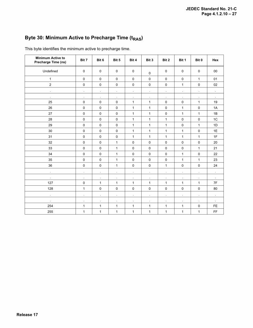
Byte 30: Minimum Active to Precharge Time (tRAS)
This byte identifies the minimum active to precharge time.
Minimum Active to Precharge Time (ns) Bit 7 Bit 6 Bit 5 Bit 4 Bit 3 Bit 2 Bit 1 Bit 0 Hex
Undefined 0 0 0 0 0 0 0 0 00
1 0 0 0 0 0 0 0 1 01
2 0 0 0 0 0 0 1 0 02
. . . . . . . . . .
. . . . . . . . . .
25 0 0 0 1 1 0 0 1 19
26 0 0 0 1 1 0 1 0 1A
27 0 0 0 1 1 0 1 1 1B
28 0 0 0 1 1 1 0 0 1C
29 0 0 0 1 1 1 0 1 1D
30 0 0 0 1 1 1 1 0 1E
31 0 0 0 1 1 1 1 1 1F
32 0 0 1 0 0 0 0 0 20
33 0 0 1 0 0 0 0 1 21
34 0 0 1 0 0 0 1 0 22
35 0 0 1 0 0 0 1 1 23
36 0 0 1 0 0 1 0 0 24
. . . . . . . . . .
. . . . . . . . . .
127 0 1 1 1 1 1 1 1 7F
128 1 0 0 0 0 0 0 0 80
. . . . . . . . . .
. . . . . . . . . .
254 1 1 1 1 1 1 1 0 FE
255 1 1 1 1 1 1 1 1 FF

Release 17
JEDEC Standard No. 21-CPage 4.1.2.10 – 28
Byte 31: Module Rank Density
This byte describes the density of each physical rank on the SDRAM DIMM. This byte will have only one bit set to “1” to represent per rank density. If there are more than one physical rank on the module (as repre-sented in byte 5), then total density can be calculated by multiplying rank density in this field by number ranks described in byte 5.
For example:
Density of Physical Rank Byte 31 Contents
512MB 1000 0000
256MB 0100 0000
Bit 7 Bit 6 Bit 5 Bit 4 Bit 3 Bit 2 Bit 1 Bit 0
512 MB 256 MB 128 MB 16 GB 8 GB 4 GB 2 GB 1 GB
0/1 0/1 0/1 0/1 0/1 0/1 0/1 0/1
1 = Supported on this assembly; 0 = Not supported on this assembly.

Release 17
JEDEC Standard No. 21-CPage 4.1.2.10 – 29
Byte 32: Address and Command Setup Time Before Clock (tIS)
This field describes the input setup time before the rising edge of the clock. The byte is broken into two nib-bles: the higher order nibble (bits 4-7) designate the access time to a granularity of 0.1 ns; the value pre-sented by the lower order nibble (bits 0-3) has the granularity of 0.01 ns and is added to the value designated by the higher nibble. Spec numbers that are in fractions of 0.01 ns will be rounded down (e.g. if the spec num-ber is 375 ps, then 0.37 [ns] will be programmed in this field). Setup and hold time numbers are to be inter-preted exactly as they are defined in JESD79-2 (Release 2).
For example:
if bits 7:4 are and bits 3:0 are then the total time is:
1011(1.1 ns)
0000+ (0 ns) = 1.1 ns
1100(1.2 ns)
0101+ (0.05 ns) = 1.25 ns
Byte 32: SDRAM Setup Time Before Clock, Subfield A: Tenths of Nanoseconds (Bits 4-7)
Line # Access from Clock Bit 7 Bit 6 Bit 5 Bit 4 Bit 3 Bit 2 Bit 1 Bit 0 Hex
0A Undefined 0 0 0 0 0_1A 0.1 ns 0 0 0 1 1_2A 0.2 ns 0 0 1 0 2_3A 0.3 ns 0 0 1 1 3_4A 0.4 ns 0 1 0 0 4_5A 0.5 ns 0 1 0 1 5_6A 0.6 ns 0 1 1 0 6_7A 0.7 ns 0 1 1 1 7_8A 0.8 ns 1 0 0 0 8_9A 0.9 ns 1 0 0 1 9_10A 1.0 ns 1 0 1 0 A_11A 1.1 ns 1 0 1 1 B_12A 1.2 ns 1 1 0 0 C_13A RFU 1 1 0 1 D_
- Undefined 1 1 1 1 1 1 1 1 FF
Byte 32: SDRAM Setup Time Before Clock, Subfield B: Hundredths of Nanoseconds (Bits 0-3)
Line # Access from Clock Bit 7 Bit 6 Bit 5 Bit 4 Bit 3 Bit 2 Bit 1 Bit 0 Hex
0B +0 ns 0 0 0 0 _01B +0.01 ns 0 0 0 1 _12B +0.02 ns 0 0 1 0 _23B +0.03 ns 0 0 1 1 _34B +0.04 ns 0 1 0 0 _45B +0.05 ns 0 1 0 1 _56B +0.06 ns 0 1 1 0 _67B +0.07 ns 0 1 1 1 _78B +0.08 ns 1 0 0 0 _89B +0.09 ns 1 0 0 1 _910B RFU 1 0 1 0 _A11B – - - - - - - - - -
- Undefined 1 1 1 1 1 1 1 1 FF
See Subfield B
See Subfield A

Release 17
JEDEC Standard No. 21-CPage 4.1.2.10 – 30
Byte 33: Address and Command Hold Time After Clock (tIH)
This field describes the input hold time after the rising edge of the clock. The byte is broken into two nibbles: the higher order nibble (bits 4-7) designate the access time to a granularity of 0.1 ns; the value presented by the lower order nibble (bits 0-3) has the granularity of 0.01 ns and is added to the value designated by the higher nibble. Spec numbers that are in fractions of 0.01 ns will be rounded down (e.g. if the spec number is 375 ps, then 0.37 [ns] will be programmed in this field). Setup and hold time numbers are to be interpreted exactly as they are defined in JESD79-2 (Release 2).
For example:
if bits 7:4 are and bits 3:0 are then the total time is:
1011(1.1 ns)
0000+ (0 ns) = 1.1 ns
1100(1.2 ns)
0101+ (0.05 ns) = 1.25 ns
Byte 33: SDRAM Hold Time After Clock, Subfield A: Tenths of Nanoseconds (Bits 4-7)
Line # Access from Clock Bit 7 Bit 6 Bit 5 Bit 4 Bit 3 Bit 2 Bit 1 Bit 0 Hex
0A Undefined 0 0 0 0 0_1A 0.1 ns 0 0 0 1 1_2A 0.2 ns 0 0 1 0 2_3A 0.3 ns 0 0 1 1 3_4A 0.4 ns 0 1 0 0 4_5A 0.5 ns 0 1 0 1 5_6A 0.6 ns 0 1 1 0 6_7A 0.7 ns 0 1 1 1 7_8A 0.8 ns 1 0 0 0 8_9A 0.9 ns 1 0 0 1 9_10A 1.0 ns 1 0 1 0 A_11A 1.1 ns 1 0 1 1 B_12A 1.2 ns 1 1 0 0 C_13A RFU 1 1 0 1 D_
- Undefined 1 1 1 1 1 1 1 1 FF
Byte 33: SDRAM Hold Time After Clock, Subfield B: Hundredths of Nanoseconds (Bits 0-3)
Line # Access from Clock Bit 7 Bit 6 Bit 5 Bit 4 Bit 3 Bit 2 Bit 1 Bit 0 Hex
0B +0 ns 0 0 0 0 _01B +0.01 ns 0 0 0 1 _12B +0.02 ns 0 0 1 0 _23B +0.03 ns 0 0 1 1 _34B +0.04 ns 0 1 0 0 _45B +0.05 ns 0 1 0 1 _56B +0.06 ns 0 1 1 0 _67B +0.07 ns 0 1 1 1 _78B +0.08 ns 1 0 0 0 _89B +0.09 ns 1 0 0 1 _910B RFU 1 0 1 0 _A11B – - - - - - - - - -
- Undefined 1 1 1 1 1 1 1 1 FF
See Subfield B
See Subfield A

Release 17
JEDEC Standard No. 21-CPage 4.1.2.10 – 31
Byte 34: Data Input Setup Time Before Strobe (tDS)
This field describes the input setup time before the rising edge of the strobe. The byte is broken into two nib-bles: the higher order nibble (bits 4-7) designates the time to a granularity of 0.1 ns; the value presented by the lower order nibble (bits 0-3) has the granularity of 0.01 ns and is added to the value designated by the higher nibble. Spec numbers that are in fractions of 0.01 ns will be rounded down (e.g. if the spec number is 375 ps, then 0.37 [ns] will be programmed in this field). Setup and hold time numbers are to be interpreted exactly as they are defined in JESD79-2 (Release 2).
For example:
if bits 7:4 are and bits 3:0 are then the total time is:
0010 0101(0.2 ns) +(0.05 ns) = 0.25 ns
Byte 34: SDRAM Setup Time Before Strobe, Subfield A: Tenths of Nanoseconds (Bits 4-7)
Line # Access from Clock Bit 7 Bit 6 Bit 5 Bit 4 Bit 3 Bit 2 Bit 1 Bit 0 Hex
0A Undefined 0 0 0 0 0_1A 0.1 ns 0 0 0 1 1_2A 0.2 ns 0 0 1 0 2_3A 0.3 ns 0 0 1 1 3_4A 0.4 ns 0 1 0 0 4_5A 0.5 ns 0 1 0 1 5_6A 0.6 ns 0 1 1 0 6_7A 0.7 ns 0 1 1 1 7_8A 0.8 ns 1 0 0 0 8_9A 0.9 ns 1 0 0 1 9_10A RFU 1 0 1 0 A_11A - 1 0 1 1 -
- Undefined 1 1 1 1 1 1 1 1 FF
Byte 34: SDRAM Setup Time Before Strobe, Subfield B: Hundredths of Nanoseconds (Bits 0-3)
Line # Access from Clock Bit 7 Bit 6 Bit 5 Bit 4 Bit 3 Bit 2 Bit 1 Bit 0 Hex
0B +0 ns 0 0 0 0 _01B +0.01 ns 0 0 0 1 _12B +0.02 ns 0 0 1 0 _23B +0.03 ns 0 0 1 1 _34B +0.04 ns 0 1 0 0 _45B +0.05 ns 0 1 0 1 _56B +0.06 ns 0 1 1 0 _67B +0.07 ns 0 1 1 1 _78B +0.08 ns 1 0 0 0 _89B +0.09 ns 1 0 0 1 _910B RFU 1 0 1 0 _A11B – - - - - - - - - -
- Undefined 1 1 1 1 1 1 1 1 FF
See Subfield B
See Subfield A

Release 17
JEDEC Standard No. 21-CPage 4.1.2.10 – 32
Byte 35: Data Input Hold Time After Strobe (tDH)
This field describes the input hold time after the rising edge of the strobe. The byte is broken into two nibbles: the higher order nibble (bits 4-7) designate the time to a granularity of 0.1 ns; the value presented by the lower order nibble (bits 0-3) has the granularity of 0.01 ns and is added to the value designated by the higher nibble. Spec numbers that are in fractions of 0.01 ns will be rounded down (e.g. if the spec number is 375 ps, then 0.37 [ns] will be programmed in this field). Setup and hold time numbers are to be interpreted exactly as they are defined in JESD79-2 (Release 2).
For example:
if bits 7:4 are and bits 3:0 are then the total time is:
0010 0101(0.2 ns) + (0.05 ns) = 0.25 ns
Byte 35: SDRAM Hold Time After Strobe, Subfield A: Tenths of Nanoseconds (Bits 4-7)
Line # Access from Clock Bit 7 Bit 6 Bit 5 Bit 4 Bit 3 Bit 2 Bit 1 Bit 0 Hex
0A Undefined 0 0 0 0 0_1A 0.1 ns 0 0 0 1 1_2A 0.2 ns 0 0 1 0 2_3A 0.3 ns 0 0 1 1 3_4A 0.4 ns 0 1 0 0 4_5A 0.5 ns 0 1 0 1 5_6A 0.6 ns 0 1 1 0 6_7A 0.7 ns 0 1 1 1 7_8A 0.8 ns 1 0 0 0 8_9A 0.9 ns 1 0 0 1 9_10A RFU 1 0 1 0 A_11A - 1 0 1 1 -
- Undefined 1 1 1 1 1 1 1 1 FF
Byte 35: SDRAM Hold Time After Strobe, Subfield B: Hundredths of Nanoseconds (Bits 0-3)
Line # Access from Clock Bit 7 Bit 6 Bit 5 Bit 4 Bit 3 Bit 2 Bit 1 Bit 0 Hex
0B +0 ns 0 0 0 0 _01B +0.01 ns 0 0 0 1 _12B +0.02 ns 0 0 1 0 _23B +0.03 ns 0 0 1 1 _34B +0.04 ns 0 1 0 0 _45B +0.05 ns 0 1 0 1 _56B +0.06 ns 0 1 1 0 _67B +0.07 ns 0 1 1 1 _78B +0.08 ns 1 0 0 0 _89B +0.09 ns 1 0 0 1 _910B RFU 1 0 1 0 _A11B – - - - - - - - - -
- Undefined 1 1 1 1 1 1 1 1 FF
See Subfield B
See Subfield A

Release 17
JEDEC Standard No. 21-CPage 4.1.2.10 – 33
Byte 36: Write Recovery Time (tWR)
This byte describes the write recovery time (tWR)
Byte 36 is split into two pieces: the higher order bits (bits 2-7) designate the time to a granularity of 1 ns; the value presented by the lower order bits (bits 0-1) has a granularity of 0.25 ns and is added to the value desig-nated by the higher bits. For example:
if bits 7:2 are and bits 1:0 are then the total time is
001111(15 ns)
00+(0.0 ns) = 15.0 ns
010010(18 ns)
11+(0.75 ns) = 18.75 ns
Byte 36, SDRAM Minimum tWR Time, Subfield A: Whole Nanoseconds (Bits 2-7)
Nanoseconds Bit 7 Bit 6 Bit 5 Bit 4 Bit 3 Bit 2 Bit 1 Bit 0
Undefined 0 0 0 0 0 0
1 ns 0 0 0 0 0 1
2 ns 0 0 0 0 1 0
3 ns 0 0 0 0 1 1
4 ns 0 0 0 1 0 0
5 ns 0 0 0 1 0 1
6 ns 0 0 0 1 1 0
7 ns 0 0 0 1 1 1
8 ns 0 0 1 0 0 0
9 ns 0 0 1 0 0 1
10 ns 0 0 1 0 1 0
: : : : : : :
: : : : : : :
61 ns 1 1 1 1 0 1
62 ns 1 1 1 1 1 0
63 ns 1 1 1 1 1 1
Byte 36, SDRAM Minimum tWR Time, Subfield B: Quarters of Nanoseconds (Bits 0-1)
Access from Clock Bit 7 Bit 6 Bit 5 Bit 4 Bit 3 Bit 2 Bit 1 Bit 0
+0 ns 0 0
+0.25 ns 0 1
+0.50 ns 1 0
+0.75 ns 1 1
See Subfield B
See Subfield A

Release 17
JEDEC Standard No. 21-CPage 4.1.2.10 – 34
Byte 37: Internal write to read command delay (tWTR)
This byte describes the internal write to read command delay (tWTR)
Byte 37 is split into two pieces: the higher order bits (bits 2-7) designate the time to a granularity of 1 ns; the value presented by the lower order bits (bits 0-1) has a granularity of 0.25 ns and is added to the value desig-nated by the higher bits. For example:
if bits 7:2 are and bits 1:0 are then the total time is
001010(10 ns)
00+(0.0 ns) = 10.0 ns
000111(7 ns)
10+(0.50 ns) = 7.5 ns
Byte 37, SDRAM Minimum tWTR Time, Subfield A: Whole Nanoseconds (Bits 2-7)
Nanoseconds Bit 7 Bit 6 Bit 5 Bit 4 Bit 3 Bit 2 Bit 1 Bit 0
Undefined 0 0 0 0 0 0
1 ns 0 0 0 0 0 1
2 ns 0 0 0 0 1 0
3 ns 0 0 0 0 1 1
4 ns 0 0 0 1 0 0
5 ns 0 0 0 1 0 1
6 ns 0 0 0 1 1 0
7 ns 0 0 0 1 1 1
8 ns 0 0 1 0 0 0
9 ns 0 0 1 0 0 1
10 ns 0 0 1 0 1 0
: : : : : : :
: : : : : : :
61 ns 1 1 1 1 0 1
62 ns 1 1 1 1 1 0
63 ns 1 1 1 1 1 1
Byte 37, SDRAM Minimum tWTR Time, Subfield B: Quarters of Nanoseconds (Bits 0-1)
Access from Clock Bit 7 Bit 6 Bit 5 Bit 4 Bit 3 Bit 2 Bit 1 Bit 0
+0 ns 0 0
+0.25 ns 0 1
+0.50 ns 1 0
+0.75 ns 1 1
See Subfield B
See Subfield A

Release 17
JEDEC Standard No. 21-CPage 4.1.2.10 – 35
Byte 38: Internal read to precharge command delay (tRTP)
This byte describes internal read to precharge command delay (tRTP)
Byte 38 is split into two pieces: the higher order bits (bits 2-7) designate the time to a granularity of 1 ns; the value presented by the lower order bits (bits 0-1) has a granularity of 0.25 ns and is added to the value desig-nated by the higher bits. For example:
if bits 7:2 are and bits 1:0 are then the total time is
001010(10 ns)
00+(0.0 ns) = 10.0 ns
000111(7 ns)
10+(0.50 ns) = 7.5 ns
Byte 38, SDRAM Minimum tRTP Time, Subfield A: Whole Nanoseconds (Bits 2-7)
Nanoseconds Bit 7 Bit 6 Bit 5 Bit 4 Bit 3 Bit 2 Bit 1 Bit 0
Undefined 0 0 0 0 0 0
1 ns 0 0 0 0 0 1
2 ns 0 0 0 0 1 0
3 ns 0 0 0 0 1 1
4 ns 0 0 0 1 0 0
5 ns 0 0 0 1 0 1
6 ns 0 0 0 1 1 0
7 ns 0 0 0 1 1 1
8 ns 0 0 1 0 0 0
9 ns 0 0 1 0 0 1
10 ns 0 0 1 0 1 0
: : : : : : :
: : : : : : :
61 ns 1 1 1 1 0 1
62 ns 1 1 1 1 1 0
63 ns 1 1 1 1 1 1
Byte 38, SDRAM Minimum tRTP Time, Subfield B: Quarters of Nanoseconds (Bits 0-1)
Access from Clock Bit 7 Bit 6 Bit 5 Bit 4 Bit 3 Bit 2 Bit 1 Bit 0
+0 ns 0 0
+0.25 ns 0 1
+0.50 ns 1 0
+0.75 ns 1 1
See Subfield B
See Subfield A

Release 17
JEDEC Standard No. 21-CPage 4.1.2.10 – 36
Byte 39: Memory Analysis Probe Characteristics
This byte describes various functional and parametric characteristics of the memory analysis probe connected to this DIMM slot. These characteristics may be consulted by the BIOS to determine proper bus drive strength to account for additional bus loading of the probe. It also describes functional characteristics of the probe that may be used to configure the memory controller to drive proper diagnostic signals to the probe, such as via the TEST,NC pin.
Detailed Features: TBD

Release 17
JEDEC Standard No. 21-CPage 4.1.2.10 – 37
Byte 40: Extension of Byte 41 tRC and Byte 42 tRFC
This field describes the extension of Byte 41 tRC and Byte 42 tRFC.
For example:
if module tRFC is:byte 40 byte 42
Bit 7 Bit 6 Bit 5 Bit 4 Bit 3 Bit 2 Bit 1 Bit 0 Bit 7 Bit 6 Bit 5 Bit 4 Bit 3 Bit 2 Bit1 Bit 0
127.5 ns 0 X X X 0 1 1 0 0 1 1 1 1 1 1 1327.5 ns 0 X X X 0 1 1 1 0 1 0 0 0 1 1 1
if module tRC is:byte 40 byte 41
Bit 7 Bit 6 Bit 5 Bit 4 Bit 3 Bit 2 Bit 1 Bit 0 Bit 7 Bit 6 Bit 5 Bit 4 Bit 3 Bit 2 Bit1 Bit 0
63.75 ns 0 1 0 1 X X X X 0 0 1 1 1 1 1 165 ns 0 0 0 0 X X X X 0 1 0 0 0 0 0 1
Byte 40: Subfield A, Extension of Byte 42 tRFC (Bits 0)
Line #Minimum Refresh to
Active/Refresh Command Period MSB
Bit 7TBD Bit 6 Bit 5 Bit 4 Bit 3 Bit 2 Bit 1 Bit 0
0A Undefined 0 01A 256 ns + byte 42 0 1
Byte 40: Subfield B, Extension of Byte 42 tRFC (Bits 1-3)
Line #Minimum Refresh to
Active/Refresh Command Period LSB
Bit 7TBD Bit 6 Bit 5 Bit 4 Bit 3 Bit 2 Bit 1 Bit 0
0B +0 ns + byte 42 0 0 0 01B +0.25 ns + byte 42 0 0 0 12B +0.33 ns + byte 42 0 0 1 03B +0.5 ns + byte 42 0 0 1 14B +0.66 ns + byte 42 0 1 0 05B +0.75 ns + byte 42 0 1 0 16B RFU 0 1 1 0- Undefined 0 1 1 1
Byte 40: Subfield C, Extension of Byte 41 tRC (Bits 4-6)
Line #Minimum Active to
Active/Refresh Command Period LSB
Bit 7TBD Bit 6 Bit 5 Bit 4 Bit 3 Bit 2 Bit 1 Bit 0
0C +0 ns + byte 41 0 0 0 01C +0.25 ns + byte 41 0 0 0 12C +0.33 ns + byte 41 0 0 1 03C +0.5 ns + byte 41 0 0 1 14C +0.66 ns + byte 41 0 1 0 05C +0.75 ns + byte 41 0 1 0 16C RFU 0 1 1 0- Undefined 0 1 1 1
See
Sub
field
A
See Subfield C
See
Sub
field
A
See Subfield B
See Subfield C See Subfield B

Release 17
JEDEC Standard No. 21-CPage 4.1.2.10 – 38
Byte 41: SDRAM Device Minimum Activate to Activate/Refresh Time (tRC)
This byte identifies the minimum activate to activate or refresh time with Byte 40 as extension. For DDR2-1066 7-7-7 speed bin, add tRP value as programmed in Byte 27 to tRAS value as programmed in Byte 30 and program this Byte accordingly.
For example:
if module tRC is:byte 40 byte 41
Bit 7 Bit 6 Bit 5 Bit 4 Bit 3 Bit 2 Bit 1 Bit 0 Bit 7 Bit 6 Bit 5 Bit 4 Bit 3 Bit 2 Bit1 Bit 0
63.75 ns 0 1 0 1 X X X X 0 0 1 1 1 1 1 165 ns 0 0 0 0 X X X X 0 1 0 0 0 0 0 1
Byte 41
Minimum Active to Active or Auto Refresh Time
(ns)
Bit 7 Bit 6 Bit 5 Bit 4 Bit 3 Bit 2 Bit 1 Bit 0 Hex
Undefined 0 0 0 0 0 0 0 0 00
1 0 0 0 0 0 0 0 1 01
2 0 0 0 0 0 0 1 0 02
. . . . . . . . . .
. . . . . . . . . .
25 0 0 0 1 1 0 0 1 19
26 0 0 0 1 1 0 1 0 1A
27 0 0 0 1 1 0 1 1 1B
28 0 0 0 1 1 1 0 0 1C
29 0 0 0 1 1 1 0 1 1D
30 0 0 0 1 1 1 1 0 1E
31 0 0 0 1 1 1 1 1 1F
32 0 0 1 0 0 0 0 0 20
33 0 0 1 0 0 0 0 1 21
34 0 0 1 0 0 0 1 0 22
35 0 0 1 0 0 0 1 1 23
36 0 0 1 0 0 1 0 0 24
. . . . . . . . . .
. . . . . . . . . .
127 0 1 1 1 1 1 1 1 7F
128 1 0 0 0 0 0 0 0 80
. . . . . . . . . .
. . . . . . . . .
254 1 1 1 1 1 1 1 0 FE
Undefined 1 1 1 1 1 1 1 1 FF

Release 17
JEDEC Standard No. 21-CPage 4.1.2.10 – 39
Byte 42: SDRAM Device Minimum Refresh to Activate/Refresh Command Period (tRFC) This byte identifies the minimum Refresh to Activate/Refresh Command Period (tRFC) with Byte 40 as exten-sion.
For example:
If the module’s tRFC is: then Byte 40 is: and Byte 42 is:
75 0XXX 0000 0100 1011
105 0XXX 0000 0110 1001
127.5 0XXX 0110 0111 1111
195 0XXX 0000 1100 0011
327.5 0XXX 0111 0100 0111
Byte 42
Minimum Refresh to Active/Refresh Command
Period(ns)
Bit 7 Bit 6 Bit 5 Bit 4 Bit 3 Bit 2 Bit 1 Bit 0 Hex
Undefined 0 0 0 0 0 0 0 0 00
1 0 0 0 0 0 0 0 1 01
2 0 0 0 0 0 0 1 0 02
. . . . . . . . . .
. . . . . . . . . .
25 0 0 0 1 1 0 0 1 19
26 0 0 0 1 1 0 1 0 1A
27 0 0 0 1 1 0 1 1 1B
28 0 0 0 1 1 1 0 0 1C
29 0 0 0 1 1 1 0 1 1D
30 0 0 0 1 1 1 1 0 1E
31 0 0 0 1 1 1 1 1 1F
32 0 0 1 0 0 0 0 0 20
33 0 0 1 0 0 0 0 1 21
34 0 0 1 0 0 0 1 0 22
35 0 0 1 0 0 0 1 1 23
36 0 0 1 0 0 1 0 0 24
. . . . . . . . . .
. . . . . . . . . .
127 0 1 1 1 1 1 1 1 7F
128 1 0 0 0 0 0 0 0 80
. . . . . . . . . .
. . . . . . . . .
254 1 1 1 1 1 1 1 0 FE
255 1 1 1 1 1 1 1 1 FF

Release 17
JEDEC Standard No. 21-CPage 4.1.2.10 – 40
Byte 43: SDRAM Device Maximum Device Cycle Time (tCK max)
This byte identifies the maximum device cycle time at any CAS latency. Byte 43 is split into two nibbles: the higher order nibble (bits 4-7) designates the cycle time to a granularity of 1 ns; the value presented by the lower order nibble (bits 0-3) has a granularity of 0.1 ns and is added to the value designated by the higher nib-ble. In addition, four lines of the lower order nibble are assigned to support +0.25, +0.33, +0.66 and +0.75.
For example:If bits 7:4 are and bits 3:0 are then the total time is:
1000 0000(8 ns) + (0 ns) = 8.0 ns
Byte 43, SDRAM Maximum Cycle Time, Subfield A: Whole Nanoseconds (Bits 4-7)
Line # Cycle Time Bit 7 Bit 6 Bit 5 Bit 4 Bit 3 Bit 2 Bit 1 Bit 0 Hex
0A Undefined 0 0 0 0 0_1A 1 ns 0 0 0 1 1_2A 2 ns 0 0 1 0 2_3A 3 ns 0 0 1 1 3_4A 4 ns 0 1 0 0 4_5A 5 ns 0 1 0 1 5_6A 6 ns 0 1 1 0 6_7A 7 ns 0 1 1 1 7_8A 8 ns 1 0 0 0 8_9A 9 ns 1 0 0 1 9_10A 10 ns 1 0 1 0 A_11A 11 ns 1 0 1 1 B_12A 12 ns 1 1 0 0 C_13A 13 ns 1 1 0 1 D_14A 14 ns 1 1 1 0 E_15A 15 ns 1 1 1 1 F_
- Undefined 1 1 1 1 1 1 1 1 FF
Byte 43, SDRAM Maximum Cycle Time Subfield B: Tenths of Nanoseconds (Bits 0-3)
Line # Cycle Time Bit 7 Bit 6 Bit 5 Bit 4 Bit 3 Bit 2 Bit 1 Bit 0 Hex
0B +0 ns
----
0 0 0 0 _01B +0.1 ns 0 0 0 1 _12B +0.2 ns 0 0 1 0 _23B +0.3 ns 0 0 1 1 _34B +0.4 ns 0 1 0 0 _45B +0.5 ns 0 1 0 1 _56B +0.6 ns 0 1 1 0 _67B +0.7 ns 0 1 1 1 _78B +0.8 ns 1 0 0 0 _89B +0.9 ns 1 0 0 1 _910B +0.25 ns 1 0 1 0 _A11B +0.33 ns 1 0 1 1 _B12B +0.66 ns 1 1 0 0 _C13B +0.75 ns 1 1 0 1 _D
- - - - - - - - - - -- Undefined 1 1 1 1 1 1 1 1 FF
See Subfield Table B
See Subfield Table B

Release 17
JEDEC Standard No. 21-CPage 4.1.2.10 – 41
Byte 44: SDRAM Device DQS-DQ Skew for DQS and associated DQ signals (tDQSQ max) This byte identifies the maximum skew between DQS and all DQ signals for each device, in hundredths of nanoseconds.
Maximum Device DQS-DQ Skew (tDQSQ
max) (ns)Bit 7 Bit 6 Bit 5 Bit 4 Bit 3 Bit 2 Bit 1 Bit 0 Hex
Undefined 0 0 0 0 0 0 0 0 00
0.01 0 0 0 0 0 0 0 1 01
0.02 0 0 0 0 0 0 1 0 02
0.03 0 0 0 0 0 0 1 1 03
0.04 0 0 0 0 0 1 0 0 04
. . . . . . . . . .
. . . . . . . . . .
0.50 0 0 1 1 0 0 1 0 32
. . . . . . . . . .
. . . . . . . . . .
0.60 0 0 1 1 1 1 0 0 3C
. . . . . . . . . .
. . . . . . . . . .
2.54 1 1 1 1 1 1 1 0 FE
2.55 1 1 1 1 1 1 1 1 FF

Release 17
JEDEC Standard No. 21-CPage 4.1.2.10 – 42
Byte 45: SDRAM Device Read Data Hold Skew Factor (tQHS)
This byte identifies the maximum skew tQHS in hundredths of nanoseconds.
For example:Read data Hold Skew
Factor (tQHS) (ns) Bit 7 Bit 6 Bit 5 Bit 4 Bit 3 Bit 2 Bit 1 Bit 0 Hex
Undefined 0 0 0 0 0 0 0 0 00
0.01 0 0 0 0 0 0 0 1 01
0.02 0 0 0 0 0 0 1 0 02
0.03 0 0 0 0 0 0 1 1 03
0.04 0 0 0 0 0 1 0 0 04
. . . . . . . . . .
. . . . . . . . . .
0.50 0 0 1 1 0 0 1 0 32
. . . . . . . . . .
. . . . . . . . . .
0.60 0 0 1 1 1 1 0 0 3C
. . . . . . . . . .
. . . . . . . . . .
2.54 1 1 1 1 1 1 1 0 FE
2.55 1 1 1 1 1 1 1 1 FF

Release 17
JEDEC Standard No. 21-CPage 4.1.2.10 – 43
Byte 46: PLL Relock Time
This byte describes the relock time of PLLs on the clock inputs in microseconds.
PLL Relock Time (μs) Bit 7 Bit 6 Bit 5 Bit 4 Bit 3 Bit 2 Bit 1 Bit 0 Hex
Undefined 0 0 0 0 0 0 0 0 00
1 0 0 0 0 0 0 0 1 01
2 0 0 0 0 0 0 1 0 02
. . . . . . . . . .
. . . . . . . . . .
25 0 0 0 1 1 0 0 1 19
26 0 0 0 1 1 0 1 0 1A
27 0 0 0 1 1 0 1 1 1B
28 0 0 0 1 1 1 0 0 1C
29 0 0 0 1 1 1 0 1 1D
30 0 0 0 1 1 1 1 0 1E
31 0 0 0 1 1 1 1 1 1F
32 0 0 1 0 0 0 0 0 20
33 0 0 1 0 0 0 0 1 21
34 0 0 1 0 0 0 1 0 22
35 0 0 1 0 0 0 1 1 23
36 0 0 1 0 0 1 0 0 24
. . . . . . . . . .
. . . . . . . . . .
127 0 1 1 1 1 1 1 1 7F
128 1 0 0 0 0 0 0 0 80
. . . . . . . . . .
. . . . . . . . . .
254 1 1 1 1 1 1 1 0 FE
255 1 1 1 1 1 1 1 1 FF

Release 17
JEDEC Standard No. 21-CPage 4.1.2.10 – 44
Byte 47: Tcasemax
This byte is split into two nibbles. The higher order nibble (bits 4:7) describes the DRAM case temperature difference between maximum case temperature and the baseline maximum case temperature of 85 0C. Unit for this field is2 0C. The DRAM maximum case temperature is 85 0C plus the value in bits 4:7. If bits 4:7 is zero, the DRAM device only supports up to 85 0C maximum case temperature and users must ensure the case temperature will not exceed 85 0C in any operation. If bits 4:7 is non-zero, the maximum case temperature range is extended and users must look at byte 49 bit 1 for the proper operation at this extended case temperature.
The lower order nibble (bits 0:3) describe DT4R4W Delta ( the DRAM case temperature rise difference from ambient due to IDD4R/page open burst read vs. IDD4W/page open burst write operations) at VDD = 1.9 V, in unit of 0.4 0C. Please refer to JEDEC DDR2 SDRAM Component Specification for the definitions of IDD4R and IDD4W operations. Please refer to Notes 6 & 7 of the ”1.1 Address Map table” of this spec for calculation of temperature rise.
Byte 47: Tcasemax, Subfield A: 2 0C (Bits 7:4)Line # Tcasemax ( Unit: 2 0C ) Bit 7 Bit 6 Bit 5 Bit 4 Bit 3 Bit 2 Bit 1 Bit 0 Hex
0A 0 0 0 0 0 0-1A 2 0 0 0 1 1-2A 4 0 0 1 0 2-3A 6 0 0 1 1
See Subfield B3-
4A 8 0 1 0 0 4-5A 10 0 1 0 1 5-6A 12 0 1 1 0 6-7A 14 0 1 1 1 7-8A 16 1 0 0 0 8-9A 18 1 0 0 1 9-
10A 20 1 0 1 0See Subfield B
A-. . . . . . .. . . . . . .
14A 28 1 1 1 0 E-15A Exceed 30 1 1 1 1 F-
Byte 47: DT4R4W Delta, Subfield B: 0.4 0C (Bits 0:3)Line # DT4R4W Delta (Granularity: 0.4 0C ) Bit 7 Bit 6 Bit 5 Bit 4 Bit 3 Bit 2 Bit 1 Bit 0 Hex
0A 0 0 0 0 0 -01A 0.4 0 0 0 1 -12A 0.8 0 0 1 0 -23A 1.2 0 0 1 1 -34A 1.6 0 1 0 0 -45A 2.0 0 1 0 1 -56A 2.4 0 1 1 0 -67A 2.8 0 1 1 1 -78A 3.2
See Subfield A1 0 0 0 -8
9A 3.6 1 0 0 1 -910A 4.0 1 0 1 0 -A
. . . . . . .
. . . . . . .14A 5.6 1 1 1 0 -E15A Exceed 6.0 1 1 1 1 -F

Release 17
JEDEC Standard No. 21-CPage 4.1.2.10 – 45
Byte 48: Thermal Resistance of DRAM Package from Top (Case) to Ambient ( Psi T-A DRAM )
This byte describes the thermal resistance of DRAM package from top (case) to ambient and it is based on JESD51-3 “Low Effective Thermal Conductivity Test Board for Leaded Surface Mount Packages” under JESD51-2 standard. Unit for this field is 0.5 oC/W.
Byte 48: Thermal Resistance of DRAM Package from Top (Case) to Ambient ( Psi T-A DRAM )
Psi T-A DRAM (Granularity: 0.5 0C/W ) Bit 7 Bit 6 Bit 5 Bit 4 Bit 3 Bit 2 Bit 1 Bit 0 HexNot Defined 0 0 0 0 0 0 0 0 00
0.5 0 0 0 0 0 0 0 1 011.0 0 0 0 0 0 0 1 0 021.5 0 0 0 0 0 0 1 1 032.0 0 0 0 0 0 1 0 0 04. . . . . . . . . .. . . . . . . . . .
16.0 0 0 1 0 0 0 0 0 32. . . . . . . . . .. . . . . . . . . .
30.0 0 0 1 1 1 1 0 0 3C. . . . . . . . . .. . . . . . . . . .
127 1 1 1 1 1 1 1 0 FEExceed 127.5 1 1 1 1 1 1 1 1 FF

Release 17
JEDEC Standard No. 21-CPage 4.1.2.10 – 46
Byte 49: DRAM Case Temperature Rise from Ambient due to Activate-Precharge/Mode Bits (DT0/Mode Bits)
This byte is split into two fields. Bits 2:7 describe DT0 ( DRAM case temperature rise from ambient due to IDD0/activate-precharge operation minus 2.8 0C offset temperature ), in unit of 0.3 0C. The value in Bits 2:7 plus 2.8 0C is the DRAM case temperature rise from ambient. Please refer to JEDEC DDR2 SDRAM Compo-nent Specification for the definition of IDD0 operation. Please refer to Notes 6 & 7 of the “1.1 Address Map table” of this spec for calculation of temperature rise.
Bit 1 definition whether or not double refresh is required for DRAM case temperature exceeding 85 0C.
Bit 0 indicates DDR2 SDRAM “High Temperature Self Refresh” support.
Byte 49: DT0, Subfield A: 0.3 0C (Bits 2:7)
Line # DT0 ( Granularity: 0.3 0C ) Bit 7 Bit 6 Bit 5 Bit 4 Bit 3 Bit 2 Bit 1 Bit 0
0A Not Defined 0 0 0 0 0 0
1A 0.3 0 0 0 0 0 1
2A 0.6 0 0 0 0 1 0
3A 0.9 0 0 0 0 1 1
4A 1.2 0 0 0 1 0 0
5A 1.5 0 0 0 1 0 1 See Sub-field B6A 1.8 0 0 0 1 1 0
7A 2.1 0 0 0 1 1 1
8A 2.4 0 0 1 0 0 0See subfield A
9A 2.7 0 0 1 0 0 1
10A 3.0 0 0 1 0 1 0
. . . . . . . .
. . . . . . . .
62A 18.6 1 1 1 1 1 0
63A Exceed 18.9 1 1 1 1 1 1
Bit 1 Byte 49: Subfield B (Bit 1)
0 Do not need double refresh rate for the proper operation at the DRAM maximum case temperature above 85 0C. The DRAM maximum case temperature is specified at Byte 47.
1 Requires double refresh rate for the proper operation at the DRAM maximum case temperature above 85 0C. The DRAM maximum case temperature is specified at Byte 47.
Bit 0 Byte 49: Subfield A (Bit 0)
0DRAM does not support high temperature self-refresh entry. Controller must ensure DRAM cools down to Tcase < 85 0C before entering self-refresh
1DRAM high temperature self-refresh entry supported. When needed, controller may set DRAM in high tempera-ture self-refresh mode via EMRS(2) [A7] and be able to enter self-refresh above 85 0C Tcase temperature

Release 17
JEDEC Standard No. 21-CPage 4.1.2.10 – 47
Byte 50: DRAM Case Temperature Rise from Ambient due to Precharge/Quiet Standby (DT2N/DT2Q)For Unbuffered DIMM, this describes the DRAM case temperature rise from ambient due to IDD2N/precharge standby operation (DT2N) at VDD = 1.9 V, in unit of 0.1 0C. Please refer to JEDEC DDR2 SDRAM Component Specification for the definition of IDD2N operation. Please refer to Notes 6 & 7 of the “1.1 Address Map table” of this spec for calculation of temperature rise.
For Registered DIMM, this byte describes the DRAM case temperature rise from ambient due to IDD2Q/pre-charge quiet standby operation (DT2Q) at VDD = 1.9 V, in unit of 0.1 0C. Please refer to JEDEC DDR2 SDRAM Component Specification for the definition of IDD2Q operation. Please refer to Notes 6 & 7 of the “1.1 Address Map table” of this spec for calculation of temperature rise.
DT2N/2Q ( Granularity: 0.1 oC ) Bit 7 Bit 6 Bit 5 Bit 4 Bit 3 Bit 2 Bit 1 Bit 0 Hex
Not Supported 0 0 0 0 0 0 0 0 00
0.1 0 0 0 0 0 0 0 1 01
0.2 0 0 0 0 0 0 1 0 02
0.3 0 0 0 0 0 0 1 1 03
0.4 0 0 0 0 0 1 0 0 04
. . . . . . . . . .
. . . . . . . . . .
3.2 0 0 1 0 0 0 0 0 32
. . . . . . . . . .
. . . . . . . . . .
6.0 0 0 1 1 1 1 0 0 3C
. . . . . . . . . .
. . . . . . . . . .
25.4 1 1 1 1 1 1 1 0 FE
Exceed 25.5 1 1 1 1 1 1 1 1 FF

Release 17
JEDEC Standard No. 21-CPage 4.1.2.10 – 48
Byte 51: DRAM Case Temperature Rise from Ambient due to Precharge Power-Down (DT2P)This byte describes the DRAM case temperature rise from ambient due to IDD2P/precharge power-down operation at VDD = 1.9 V, in unit of 0.015 0C. Please refer to JEDEC DDR2 SDRAM Component Specification for IDD2P operation. Please refer to Notes 6 & 7 of the “1.1 Address Map table” of this spec for calculation of temperature rise.
Byte 52: DRAM Case Temperature Rise from Ambient due to Active Standby (DT3N)This byte describes the DRAM case temperature rise from ambient due to IDD3N/active standby operation at VDD = 1.9 V, in unit of 0.15 0C. Please refer to JEDEC DDR2 SDRAM Component Specification for IDD3N operation. Please refer to Notes 6 & 7 of the “1.1 Address Map table” of this spec for calculation of temperature rise.
DT2P ( Granularity: 0.015 oC ) Bit 7 Bit 6 Bit 5 Bit 4 Bit 3 Bit 2 Bit 1 Bit 0 HexNot Supported 0 0 0 0 0 0 0 0 00
0.015 0 0 0 0 0 0 0 1 010.030 0 0 0 0 0 0 1 0 020.045 0 0 0 0 0 0 1 1 030.060 0 0 0 0 0 1 0 0 04
. . . . . . . . . .
. . . . . . . . . .0.480 0 0 1 0 0 0 0 0 32
. . . . . . . . . .
. . . . . . . . . .0.900 0 0 1 1 1 1 0 0 3C
. . . . . . . . . .
. . . . . . . . . .3.810 1 1 1 1 1 1 1 0 FE
Exceed 3.825 1 1 1 1 1 1 1 1 FF
DT3N ( Granularity: 0.15 oC ) Bit 7 Bit 6 Bit 5 Bit 4 Bit 3 Bit 2 Bit 1 Bit 0 HexNot Supported 0 0 0 0 0 0 0 0 00
0.15 0 0 0 0 0 0 0 1 010.30 0 0 0 0 0 0 1 0 020.45 0 0 0 0 0 0 1 1 030.60 0 0 0 0 0 1 0 0 04
. . . . . . . . . .
. . . . . . . . . .4.80 0 0 1 0 0 0 0 0 32
. . . . . . . . . .
. . . . . . . . . .9.00 0 0 1 1 1 1 0 0 3C
. . . . . . . . . .
. . . . . . . . . .38.10 1 1 1 1 1 1 1 0 FE
Exceed 38.25 1 1 1 1 1 1 1 1 FF

Release 17
JEDEC Standard No. 21-CPage 4.1.2.10 – 49
Byte 53: DRAM Case temperature Rise from Ambient due to Active Power-Down with Fast PDN Exit (DT3Pfast)This byte describes the DRAM case temperature rise from ambient due to IDD3P Fast PDN Exit/active power-down with fast PDN exit operation at VDD = 1.9 V, in unit of 0.05 0C. Please refer to JEDEC DDR2 SDRAM Component Specification for IDD3P Fast PDN Exit operation. Please refer to Notes 6 & 7 of the “1.1 Address Map table” of this spec for calculation of temperature rise.
Byte 54: DRAM Case temperature Rise from Ambient due to Active Power-Down with Slow PDN Exit (DT3Pslow)This byte describes the DRAM case temperature rise from ambient due to IDD3P Slow PDN Exit/active power-down with slow PDN exit operation at VDD = 1.9 V, in unit of 0.025 0C. Please refer to JEDEC DDR2 SDRAM Component Specification for IDD3P Slow PDN Exit operation. Please refer to Notes 6 & 7 of the “1.1 Address Map table” of this spec for calculation of temperature rise.
DT3Pfast ( Granularity: 0.05 oC ) Bit 7 Bit 6 Bit 5 Bit 4 Bit 3 Bit 2 Bit 1 Bit 0 HexNot Supported 0 0 0 0 0 0 0 0 00
0.05 0 0 0 0 0 0 0 1 010.10 0 0 0 0 0 0 1 0 020.15 0 0 0 0 0 0 1 1 030.20 0 0 0 0 0 1 0 0 04
. . . . . . . . . .
. . . . . . . . . .1.60 0 0 1 0 0 0 0 0 32
. . . . . . . . . .
. . . . . . . . . .3.00 0 0 1 1 1 1 0 0 3C
. . . . . . . . . .
. . . . . . . . . .12.70 1 1 1 1 1 1 1 0 FE
Exceed 12.75 1 1 1 1 1 1 1 1 FF
DT3Pslow ( Granularity: 0.025 oC ) Bit 7 Bit 6 Bit 5 Bit 4 Bit 3 Bit 2 Bit 1 Bit 0 HexNot Supported 0 0 0 0 0 0 0 0 00
0.025 0 0 0 0 0 0 0 1 010.050 0 0 0 0 0 0 1 0 020.075 0 0 0 0 0 0 1 1 030.100 0 0 0 0 0 1 0 0 04
. . . . . . . . . .
. . . . . . . . . .0.800 0 0 1 0 0 0 0 0 32
. . . . . . . . . .
. . . . . . . . . .1.500 0 0 1 1 1 1 0 0 3C
. . . . . . . . . .
. . . . . . . . . .6.350 1 1 1 1 1 1 1 0 FE
Exceed 6.375 1 1 1 1 1 1 1 1 FF

Release 17
JEDEC Standard No. 21-CPage 4.1.2.10 – 50
Byte 55: DRAM Case Temperature Rise from Ambient due to Page Open Burst Read/DT4R4W Mode Bit (DT4R/DT4R4W Mode Bit)This byte is split into two fields: bits 1:7 describes the DRAM case temperature rise from ambient due to IDD4R/page open read operation at VDD = 1.9 V, in unit of 0.4 0C. Please refer to JEDEC DDR2 SDRAM Component Specifica-tion for the definition of IDD4R operation. Please refer to Notes 6 & 7 of the “1.1 Address Map table” of this spec for calculation of temperature rise. Bit 0 specifies if DT4W ( Case temperature rise from ambient due to page open burst write) is greater than or less than DT4R.
Byte 55: DT4R, Subfield A: 0.4 0C ( Bits 1:7 )
Line # DT4R (Granularity: 0.4 oC ) Bit 7 Bit 6 Bit 5 Bit 4 Bit 3 Bit 2 Bit 1 Bit 0
0A Not Supported 0 0 0 0 0 0 0
1A 0.4 0 0 0 0 0 0 1
2A 0.8 0 0 0 0 0 1 0
3A 1.2 0 0 0 0 0 1 1
4A 1.6 0 0 0 0 1 0 0
5A 2.0 0 0 0 0 1 0 1See Sub-
field B6A 2.4 0 0 0 0 1 1 1
7A 2.8 0 0 0 1 0 0 0
8A 3.2 0 0 0 1 0 0 1
9A 3.6 0 0 0 1 0 1 0
10A 4.0 0 0 0 1 0 1 1
. . . . . . . . .
. . . . . . . . .
126A 50.4 1 1 1 1 1 1 0
127A Exceed 50.8 1 1 1 1 1 1 1
Byte 55: DT4R4W Mode Bit, Subfield B: 0.4 0C ( Bit 0 )
Line # DT4R4W Mode Bit Bit 7 Bit 6 Bit 5 Bit 4 Bit 3 Bit 2 Bit 1 Bit 0
0A DT4W is greater than or equal to DT4RSee Subfield A
0
1A DT4W is less than DT4R 1

Release 17
JEDEC Standard No. 21-CPage 4.1.2.10 – 51
Byte 56: DRAM Case Temperature Rise from Ambient due to Burst Refresh (DT5B)This byte describes the DRAM case temperature rise from ambient due to IDD5B/burst refresh operation at VDD = 1.9 V, in unit of 0.5 0C. Please refer to JEDEC DDR2 SDRAM Component Specification for the definition of IDD5B operation. Please refer to Notes 6 & 7 of the “1.1 Address Map table” of this spec for calculation of temperature rise.
Byte 57: DRAM Case Temperature Rise from Ambient due to Bank Interleave Reads with Auto-Precharge (DT7)This byte describes the DRAM case temperature rise from ambient due to IDD7/bank interleave read with auto-pre-charge operation at VDD = 1.9 V, in unit of 0.5 0C. Please refer to Notes 6 & 7 of the “1.1 Address Map table” of this spec for calculation of temperature rise.
DT5B (Granularity: 0.5 oC ) Bit 7 Bit 6 Bit 5 Bit 4 Bit 3 Bit 2 Bit 1 Bit 0 Hex
Not Supported 0 0 0 0 0 0 0 0 00
0.5 0 0 0 0 0 0 0 1 01
1.0 0 0 0 0 0 0 1 0 02
1.5 0 0 0 0 0 0 1 1 03
2.0 0 0 0 0 0 1 0 0 04
. . . . . . . . . .
. . . . . . . . . .
16.0 0 0 1 0 0 0 0 0 32
. . . . . . . . . .
. . . . . . . . . .
30.0 0 0 1 1 1 1 0 0 3C
. . . . . . . . . .
. . . . . . . . . .
127.0 1 1 1 1 1 1 1 0 FE
Exceed 127.5 1 1 1 1 1 1 1 1 FF
DT7 (Granularity: 0.5 oC ) Bit 7 Bit 6 Bit 5 Bit 4 Bit 3 Bit 2 Bit 1 Bit 0 Hex
Not Supported 0 0 0 0 0 0 0 0 00
0.5 0 0 0 0 0 0 0 1 01
1.0 0 0 0 0 0 0 1 0 02
1.5 0 0 0 0 0 0 1 1 03
2.0 0 0 0 0 0 1 0 0 04
. . . . . . . . . .
. . . . . . . . . .
16.0 0 0 1 0 0 0 0 0 32
. . . . . . . . . .
. . . . . . . . . .
30.0 0 0 1 1 1 1 0 0 3C
. . . . . . . . . .
. . . . . . . . . .
127.0 1 1 1 1 1 1 1 0 FE
Exceed 127.5 1 1 1 1 1 1 1 1 FF

Release 17
JEDEC Standard No. 21-CPage 4.1.2.10 – 52
Byte 58: Thermal Resistance of PLL Package from Top (Case) to Ambient ( Psi T-A PLL )This byte describes the thermal resistance of PLL package from top (case) to ambient and it is based on JESD51-3 “Low Effective Thermal Conductivity Test Board for Leaded Surface Mount Packages” under JESD51-2 standard. Unit for this byte is 0.5 0C/W.
Byte 59: Thermal Resistance of Register Package from Top (Case) to Ambient ( Psi T-A Reg-ister)This byte describes the thermal resistance of register package from top (case) to ambient and it is based on JESD51-3 “Low Effective Thermal Conductivity Test Board for Leaded Surface Mount Packages” under JESD51-2 standard. Unit for this byte is 0.5 0C/W.
Byte 58: Thermal Resistance of PLL Package from Top (Case) to Ambient ( Psi T-A PLL )
Psi T-A PLL(Granularity: 0.5 0C/W ) Bit 7 Bit 6 Bit 5 Bit 4 Bit 3 Bit 2 Bit 1 Bit 0 HexNot Supported 0 0 0 0 0 0 0 0 00
0.5 0 0 0 0 0 0 0 1 011.0 0 0 0 0 0 0 1 0 021.5 0 0 0 0 0 0 1 1 032.0 0 0 0 0 0 1 0 0 04. . . . . . . . . .. . . . . . . . . .
16.0 0 0 1 0 0 0 0 0 32. . . . . . . . . .. . . . . . . . . .
30.0 0 0 1 1 1 1 0 0 3C. . . . . . . . . .. . . . . . . . . .
127 1 1 1 1 1 1 1 0 FEExceed 127.5 1 1 1 1 1 1 1 1 FF
Byte 59: Thermal Resistance of Register Package from Top (Case) to Ambient ( Psi T-A Register)
Psi T-A Register (Granularity: 0.5 0C/W ) Bit 7 Bit 6 Bit 5 Bit 4 Bit 3 Bit 2 Bit 1 Bit 0 Hex
Not Supported 0 0 0 0 0 0 0 0 00
0.5 0 0 0 0 0 0 0 1 01
1.0 0 0 0 0 0 0 1 0 02
1.5 0 0 0 0 0 0 1 1 03
2.0 0 0 0 0 0 1 0 0 04
. . . . . . . . . .
. . . . . . . . . .
16.0 0 0 1 0 0 0 0 0 32
. . . . . . . . . .
. . . . . . . . . .
30.0 0 0 1 1 1 1 0 0 3C
. . . . . . . . . .
. . . . . . . . . .
127 1 1 1 1 1 1 1 0 FE
Exceed 127.5 1 1 1 1 1 1 1 1 FF

Release 17
JEDEC Standard No. 21-CPage 4.1.2.10 – 53
Byte 60: PLL Case Temperature Rise from Ambient due to PLL Active (DT PLL Active)This byte describes the PLL case temperature rise from ambient due to PLL in active mode with clock running within spec and OE enabled and at VDD = 1.9 V, in unit of 0.25 0C. The PLL loading is the DIMM loading. Registers being used in the DIMM may have different variants, like single rank, dual ranks, dual ranks without parity. This SPD field needs to correspond to the respective DIMM configuration. Please refer to Byte 21 to determine the number of PLLs on the DIMM. Please refer to Notes 9 & 11 of the “1.1 Address Map table” of this spec for calculation of temperature rise.
DT PLL Active (Granularity: 0.25 oC ) Bit 7 Bit 6 Bit 5 Bit 4 Bit 3 Bit 2 Bit 1 Bit 0 Hex
Not Supported 0 0 0 0 0 0 0 0 00
0.25 0 0 0 0 0 0 0 1 01
0.50 0 0 0 0 0 0 1 0 02
0.75 0 0 0 0 0 0 1 1 03
1.00 0 0 0 0 0 1 0 0 04
. . . . . . . . . .
. . . . . . . . . .
8.00 0 0 1 0 0 0 0 0 32
. . . . . . . . . .
. . . . . . . . . .
15.00 0 0 1 1 1 1 0 0 3C
. . . . . . . . . .
. . . . . . . . . .
63.50 1 1 1 1 1 1 1 0 FE
Exceed 63.75 1 1 1 1 1 1 1 1 FF

Release 17
JEDEC Standard No. 21-CPage 4.1.2.10 – 54
Byte 61: Register Case Temperature Rise from Ambient due to Register Active/Mode Bit (DT Register Active/Mode Bit)This byte is split into two fields. Bits 2:7 describes the register case temperature rise from ambient due to register in active mode with clock running within spec and OE enabled and at VDD = 1.9 V. The register loading is the registered DIMM loading. Registers being used in registered DIMM may have different variants, like single rank, dual ranks, dual ranks without parity. This SPD field needs to correspond to the respective Registered DIMM configuration. Please refer to Notes 9 & 11 of the “1.1 Address Map table” of this spec for calculation of temperature rise. If there are multi-ple register components on the registered DIMM, this byte is still calculated using the IDD value of one of the regis-ters. Please refer to Byte 21 to determine the number of registers on the DIMM. Bit 1 is reserved for future use (RFU). Default value is 0. Bit 0 specifies the register data output toggle rate and it shall be consistent with the maxi-mum data toggle rate specified in the IDD specification in the JEDEC DDR2 SDRAM Component Specification.
Byte 61: DT Register Active, Subfield A: ( Bit 0 )Line # DT Register Active Mode Bit Bit 7 Bit 6 Bit 5 Bit 4 Bit 3 Bit 2 Bit 1 Bit 0
0A 50% register data output toggleSee Subfield B RFU.
Default: 00
1A 100% register data output toggle 1
If Bit 0 Unit for Bits 2:7 ( oC )0 0.751 1.25
Byte 61: DT Register Active, Subfield B: 0.75 0C ( Bits 2:7 ) if Bit 0 = 0Line # DT Register Active (Granularity: 0.75 oC ) Bit 7 Bit 6 Bit 5 Bit 4 Bit 3 Bit 2 Bit 1 Bit 0
0A Not Supported 0 0 0 0 0 01A 0.75 0 0 0 0 0 12A 1.50 0 0 0 0 1 0
RFU.Default: 0
Value = 0. See Sub-
field A3A 2.25 0 0 0 0 1 14A 3.00 0 0 0 1 0 05A 3.75 0 0 0 1 0 16A 4.50 0 0 0 1 1 07A 5.25 0 0 0 1 1 18A 6.00 0 0 1 0 0 09A 6.75 0 0 1 0 0 1
10A 7.50 0 0 1 0 1 0. . . . . . . .
62A 46.50 1 1 1 1 1 063A Exceed 47.25 1 1 1 1 1 1
Byte 61: DT Register Active, Subfield B: 1.25 0C ( Bits 2:7 ) if Bit 0 = 1Line # DT Register Active (Granularity: 1.25 oC ) Bit 7 Bit 6 Bit 5 Bit 4 Bit 3 Bit 2 Bit 1 Bit 0
0A Not Supported 0 0 0 0 0 01A 1.25 0 0 0 0 0 12A 2.50 0 0 0 0 1 03A 3.75 0 0 0 0 1 14A 5.00 0 0 0 1 0 05A 6.25 0 0 0 1 0 1
RFU. Default: 0
Value = 1. See Sub-
field A6A 7.50 0 0 0 1 1 07A 8.75 0 0 0 1 1 18A 10.00 0 0 1 0 0 09A 11.25 0 0 1 0 0 110A 12.50 0 0 1 0 1 0
. . . . . . . .
. . . . . . . .62A 77.5 1 1 1 1 1 063A Exceed 78.75 1 1 1 1 1 1

Release 17
JEDEC Standard No. 21-CPage 4.1.2.10 – 55
An Illustration Example of DT in SPDThis section shows an example of programming SPD Byte 21 bit 3:0 and Byte 47 ~ 61. All the numbers in the tables below are arbitrary and for the sole purpose of demonstrating how to program SPD Byte 21 bit 3:0 and Byte 47 ~ 61. They are NOT intended to reflect any actual device properties.
In the example listed in the table above, Psi T-A DRAM true value is 63.2 oC/W and unit is 0.5 oC/W, Byte value is determined as following: 63.2 / 0.5 = 126.4. Since 126.4 is closer to 126 then it is to 127, therefore the programmed SPD Byte value is rounded off to 126.
Also in the example listed in the table above, SPD Byte value for DT3P fast is calculated as following:
DT3P fast= IDD3P fast* 1.9 Volt * Programmed value of Psi T-A DRAM
= 11 mA * 1.9 V * ( Value in Byte 48 * Byte 48 Unit)
= 11 mA * 1.9 V * (126 * 0.5 0C/W)
= 1.32 oC
DT3P fast SPD byte unit is 0.05 oC, 1.32 oC/ 0.05 oC = 26.4. Since 26.4 is closer to 26 than it is to 27, therefore the programmed value for SPD byte 53 (DT3P fast) is rounded off to 26 (Hex value 1A).
DT in SPD Example For Reference Only
BYTE Bit 7
Bit 6
Bit 5
Bit 4
Bit 3
Bit 2
Bit 1
Bit 0 Hex Parameter Description Parameter
ValueByte Value
Byte Unit
21 - - - - 0 1 0 0 -4 Number of PLLs/active registers on the DIMM 1 / 1 -4
1 PLL / 1 active reg-
ister
47 0 0 0 0 0 0 1 0 02 Tcasemax / DT4R4W Delta = DT (7 mA) 85 oC/0.84 oC 0 / 2 0.4 oC
48 0 1 1 1 1 1 1 0 7E Psi T-A DRAM 63.2 oC/W 126 0.5 oC/W
49 0 1 0 0 0 1 0 -Bit 7:1: 22
DT0 = DT (65 mA) /Tcase Mode Bits4.98 oC / Do
not need dou-ble refresh.
Bit 7:2 / Bit 1:17 / 0
0.3 oC
50(UDIMM)
0 0 1 0 0 0 1 0 22 DT2N = DT (28 mA) 3.35 oC 34 0.1 oC
50(RDIMM)
0 0 0 1 0 1 1 1 17 DT2Q = DT (19 mA) 2.27 oC 23 0.1 oC
51 0 0 0 1 1 0 0 0 18 DT2P = DT (3 mA) 0.36 oC 24 0.015oC
52 0 0 0 1 1 0 0 1 19 DT3N = DT (31 mA) 3.71 oC 25 0.15 oC
53 0 0 0 1 1 0 1 0 1A DT3P fast = DT (11 mA) 1.32 oC 26 0.05 oC
54 0 0 0 1 1 0 0 0 18 DT3P slow = DT (5 mA) 0.60 oC 24 0.025 oC
55 0 0 1 0 1 0 1 0 2A DT4R = DT(70 mA) / DT4R4W Mode bit 8.38 oC/0 21 0.4 oC
56 0 0 0 1 1 1 1 1 1F DT5B = DT (128 mA) 15.32 oC 31 0.5 oC
57 0 0 1 0 1 0 0 0 28 DT7 = DT (165 mA) 19.8 oC 40 0.5 oC
58 1 0 1 1 0 1 0 0 B4 Psi T-A PLL 90 oC/W 180 0.5 oC/W
59 1 0 1 0 0 0 0 0 A0 Psi T-A Register 80 oC/W 160 0.5 oC/W
60 0 1 0 0 0 1 0 0 44 DT PLL Active = DT (100 mA) 17.1 oC 68 0.25 oC
61 0 1 1 1 1 0 RFU(0) 0 78 DT Register Active = DT (150 mA) 22.8 oC/0 30 0.75 oC
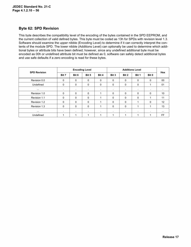
Release 17
JEDEC Standard No. 21-CPage 4.1.2.10 – 56
Byte 62: SPD Revision
This byte describes the compatibility level of the encoding of the bytes contained in the SPD EEPROM, and the current collection of valid defined bytes. This byte must be coded as 13h for SPDs with revision level 1.3. Software should examine the upper nibble (Encoding Level) to determine if it can correctly interpret the con-tents of the module SPD. The lower nibble (Additions Level) can optionally be used to determine which addi-tional bytes or attribute bits have been defined; however, since any undefined additional byte must be encoded as 00h or undefined attribute bit must be defined as 0, software can safely detect additional bytes and use safe defaults if a zero encoding is read for these bytes.
SPD RevisionEncoding Level Additions Level
HexBit 7 Bit 6 Bit 5 Bit 4 Bit 3 Bit 2 Bit 1 Bit 0
Revision 0.0 0 0 0 0 0 0 0 0 00
Undefined 0 0 0 0 0 0 0 1 01
... . . . . . . . . .
Revision 1.0 0 0 0 1 0 0 0 0 10
Revision 1.1 0 0 0 1 0 0 0 1 11
Revision 1.2 0 0 0 1 0 0 1 0 12
Revision 1.3 0 0 0 1 0 0 1 1 13
... . . . . . . . . ...
Undefined 1 1 1 1 1 1 1 1 FF
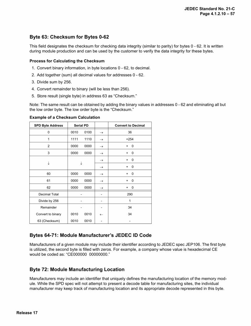
Release 17
JEDEC Standard No. 21-CPage 4.1.2.10 – 57
Byte 63: Checksum for Bytes 0-62
This field designates the checksum for checking data integrity (similar to parity) for bytes 0 - 62. It is written during module production and can be used by the customer to verify the data integrity for these bytes.
Process for Calculating the Checksum1. Convert binary information, in byte locations 0 - 62, to decimal.
2. Add together (sum) all decimal values for addresses 0 - 62.
3. Divide sum by 256.
4. Convert remainder to binary (will be less than 256).
5. Store result (single byte) in address 63 as “Checksum.”
Note: The same result can be obtained by adding the binary values in addresses 0 - 62 and eliminating all but the low order byte. The low order byte is the “Checksum.”
Bytes 64-71: Module Manufacturer’s JEDEC ID Code
Manufacturers of a given module may include their identifier according to JEDEC spec JEP106. The first byte is utilized, the second byte is filled with zeros. For example, a company whose value is hexadecimal CE would be coded as: “CE000000 00000000.”
Byte 72: Module Manufacturing Location
Manufacturers may include an identifier that uniquely defines the manufacturing location of the memory mod-ule. While the SPD spec will not attempt to present a decode table for manufacturing sites, the individual manufacturer may keep track of manufacturing location and its appropriate decode represented in this byte.
Example of a Checksum Calculation
SPD Byte Address Serial PD Convert to Decimal
0 0010 0100 → 36
1 1111 1110 → +254
2 0000 0000 → + 0
3 0000 0000 → + 0
↓ ↓→ + 0
→ + 0
60 0000 0000 → + 0
61 0000 0000 → + 0
62 0000 0000 → + 0
Decimal Total - - 290
Divide by 256 - - 1
Remainder - - 34
Convert to binary 0010 0010 ← 34
63 (Checksum) 0010 0010 - -

Release 17
JEDEC Standard No. 21-CPage 4.1.2.10 – 58
Bytes 73-90: Module Part Number
The manufacturer’s part number is written in ASCII format within these bytes. Unused digits are coded as ASCII blanks (20h).
Bytes 91-92: Module Revision Code
This refers to the module revision code. While the SPD spec will not attempt to define the format for this infor-mation, the individual manufacturer may keep track of the revision code and its appropriate decode repre-sented in this byte.
Bytes 93-94: Module Manufacturing Date
The module manufacturer includes a date code for the module. The JEDEC definitions for bytes 93 and 94 are year and week respectively. These bytes must be represented in Binary Coded Decimal (BCD). For example, week 47 in year 2003 would be coded as 03 (0000 0011) in byte 93 and 47 (0100 0111) in byte 94.
Bytes 95-98: Module Serial Number
The supplier must include a unique serial number for the module. The supplier may use whatever decode method desired to maintain a unique serial number for each module.
One method of achieving this is by assigning a byte in the field from 95-98 as a tester ID byte and using the remaining bytes as a sequential serial number. Using bytes 64-72 and 93-98 to construct a unique serial number results in a field that contains 15 bytes of data. A shortened unique serial number containing 9 bytes of data can be derived from the SPD bytes by reducing the manufacturers ID in bytes 64-71 to 2 bytes, where the first byte indicates the quantity of 0x7F “continuation characters” in bytes 64-71, and the second byte is the 1-byte manufacturers ID following the last 0x7F “continuation character” (ref: JEDEC JEP106N), Any characters following the 1-byte manufacturers ID are ignored for the purposes of constructing the value of the shortened unique serial number.
Bytes 99-127: Manufacturer’s Specific Data
The module manufacturer may include any additional information desired into the module within these loca-tions.
Bytes 128-255: Open for Customer Use
These bytes are unused by the manufacturer and are open for customer use.

Release 17
JEDEC Standard No. 21-CPage 4.1.2.10 – 59
Appendix: ASCII Decode Matrix for SPDs
The following table is a subset of the full ASCII standard which is used for coding bytes in the Serial Presence Detect EEPROM that require ASCII characters:
Examples:20h=Blank Space34h=441h=A
Second Hex Digit in Pair
First HexDigit in Pair 0 1 2 3 4 5 6 7 8 9 A B C D E F
2 BlankSpace ( ) -
Dash .
3 0 1 2 3 4 5 6 7 8 9
4 A B C D E F G H I J K L M N O
5 P Q R S T U V W X Y Z
6 a b c d e f g h i j k l m n o
7 p q r s t u v w x y z
SPD Bytes 73-90
Manufacturer’s PN Coded in ASCII
13M32734BCD-260Y 31334D33323733344243442D323630592020

Release 17
JEDEC Standard No. 21-CPage 4.1.2.10 – 60
Revision Log Date SPD Rev Doc Rel Contents of Modification
Aug 29, 2007 1.3 1
Editorial corrections in examples for bytes 23 and 25.1. Byte 9, Byte 23, Byte 25 - Added note to guide how to program SPD for DDR2 1066 sup-port.2. Byte 18 - Added CL7 support3. Byte 27, Byte 29 - Added note to guide how to program 13.125 ns for DDR2 1066 7-7-7 speed bin.4. Byte 41 - Added note to guide how to program tRC for DDR2 1066 7-7-7 speed bin.5. Byte 62 - Updated SPD revision to 1.3
June 2007 1.2 3 Editorially added field encodings for 72b-SO-DIMM to bytes 19 and 20
Mar. 2006 1.2 2
Editorial corrections to 1.2 approved1. Byte 3, extended range of addressing for new device densities2. Byte 47, subfield B, defined 0A case for case when DT4W = DT4R3. Byte 55, subfield B, changed “DT4W is greater than DT4R“ to “DT4W is greater than or equal to DT4R”
Nov. 2004 1.2 1
Revision 1.2 approved1. Added 50ohm ODT and CL = 6 to Byte 18 and 22 respectively. JC-45-04-64 passed at March 2004 meeting2. Added PASR supportability bit to Byte 22. JC-45-04-1343. Added DIMM thickness to Byte 19, and changed Byte 20 format for better description. JC-45-04-138, -139, -140, and -1414. Corrected typo on units for byte 45.
Feb. 2004 1.1 1
Revision 1.1 approved1. Changed “ Wording of Byte 93 and 94” - rb03170 passed committee ballot at Sep. 03 meet-ing2. Added Command and Address Parity feature to Byte 11 - rb03230 passed committee ballot at Dec. 03 meeting3. Added number of PLL and register feature on Byte 21 bits [3:0] - rb03246 passed commit-tee ballot at Dec. 03 meeting4. Added Byte 47 ~ 61, DT in SPD - rb03246 passed committee ballot at Dec. 03 meeting5. Added “Self refresh period at high temp” feature to Byte 49 - rb03247 passed committee ballot at Dec. 03 meeting6. Corrected typos
Feb. 2003 1.0 1 First release - BoD approved DDR2 SPD revision 1.0