analysis of impact of transformer …raiith.iith.ac.in/973/1/ee09g008.pdfanalysis of impact of...
TRANSCRIPT

ANALYSIS OF IMPACT OF TRANSFORMER COUPLED
INPUT MATCHING ON CONCURRENT DUAL-BAND LOW
NOISE AMPLIFIER
Rajendra P
A Dissertation Submitted to
Indian Institute of Technology Hyderabad
In Partial Fulfillment of the Requirements for
The Degree of Master of Technology
Department of Electrical Engineering
September, 2011
i
ii

iii
Acknowledgements
First and foremost, I would like to thank my Project Advisors Dr. Ashudeb Dutta and Dr. Shiv
Govind Singh for their expert guidance and support throughout my research work. I benefited greatly
from their expertise in the fields of analog circuit design and micro electronics.
I would like express my gratitude to Mr. A R Aravinth Kumar for his help and support.
I would also like to thank my parents for their support of all aspects of my life, but especially
of my education.

iv
Abstract
Emerging advancements in telecommunication system need robust radio devices which can
capable of working multiple frequency bands seamlessly. In any Radio Frequency (RF) receiver
architecture, Low Noise Amplifier (LNA) is the mandatory front-end part in which takes place in
between antenna and mixer. To support multiple frequency bands with single hardware, concurrent
LNA is the more preferred topologies among others.
As LNA is the very front end level of receiver, Input matching, Noise Figure (NF) and gain
are the major performance parameters to be concerned. In this work, the impact of transformer
coupled input matching on concurrent dual-band LNA is analyzed and verified. A concurrent LNA
with concurrent matching without transformer coupling is used for comparison. A transformer
coupled input matching is proposed for tunable concurrent dual-band LNA. All the circuits are
implemented in UMC 180nm CMOS technology, and simulated using Cadence SpectreRF simulation
tool.
v
Contents:
Declaration . . . . . . . . . . . . . . . . . . . . . . . . . . . . . . . . . . . . . . . . . . . . . . i
Approval Sheet . . . . . . . . . . . . . . . . . . . . . . . . . . . . . . . . . . . . . . . . . . . . ii
Acknowledgements . . . . . . . . . . . . . . . . . . . . . . . . . . . . . . . . . . . . . . . . . .iii
Abstract . . . . . . . . . . . . . . . . . . . . . . . . . . . . . . . . . . . . . . . . . . . . . . . . iv
1. Introduction
1.1 Aim and Motivation . . . . . . . . . . . . . . . . . . . . . . . . . . . . . . . . . . . . . . . . 1
1.2 Literature Survey . . . . . . . . . . . . . . . . . . . . . . . . . . . . . . . . . . . . . . . . . . . 2
1.3 Contribution of the Thesis . . . . . . . . . . . . . . . . . . . . . . . . . . . . . . . . . . . . . . 2
1.4 Low Noise Amplifier . . . . . . . . . . . . . . . . . . . . . . . . . . . . . . . . . . . . . . . . . 2
1.5 Requirement of dual band LNA . . . . . . . . . . . . . . . . . . . . . . . . . . . . . . . . . . . 4
2. CMOS LNA Fundamentals
2.1 Introduction . . . . . . . . . . . . . . . . . . . . . . . . . . . . . . . . . . . . . . . . . . . . . . . 5
2.2 Input impedance . . . . . . . . . . . . . . . . . . . . . . . . . . . . . . . . . . . . . . . . . . . . 5
2.3 Voltage Gain . . . . . . . . . . . . . . . . . . . . . . . . . . . . . . . . . . . . . . . . . . . . . . 6
2.4 Inductive Source Degeneration
2.4.1 Input impedance match . . . . . . . . . . . . . . . . . . . . . . . . . . . . . . 6
2.4.2 Effective Trans-conductance of Matched Device . . . . . . . . . . . . 6
3. Transformer coupled input matching for narrow band LNA
3.1 Introduction . . . . . . . . . . . . . . . . . . . . . . . . . . . . . . . . . . . . . . . . . . . . . 9
3.2 Target structure . . . . . . . . . . . . . . . . . . . . . . . . . . . . . . . . . . . . . . . . . . . . . 10
3.3 Input impedance . . . . . . . . . . . . . . . . . . . . . . . . . . . . . . . . . . . . . . . . . . . . . 12
3.4 Output impedance . . . . . . . . . . . . . . . . . . . . . . . . . . . . . . . . . . . . . . . . . . . 12
3.5 Gain . . . . . . . . . . . . . . . . . . . . . . . . . . . . . . . . . . . . . . . . . . . . . . . . . . 13
3.6 Simulations and Results. . . . . . . . . . . . . . . . . . . . . . . . . . . . . . . . . . . . . . . 14
3.7 Conclusion . . . . . . . . . . . . . . . . . . . . . . . . . . . . . . . . . . . . . . . 14
vi
4. Concurrent Dual-Band LNA
4.1 Introduction . . . . . . . . . . . . . . . . . . . . . . . . . . . . . . . . . . . . . . . 15
4.2 Target structure . . . . . . . . . . . . . . . . . . . . . . . . . . . . . . . . . . . . . . . 16
4.3 Input impedance . . . . . . . . . . . . . . . . . . . . . . . . . . . . . . . . . . . . . . . 16
4.4 Output impedance . . . . . . . . . . . . . . . . . . . . . . . . . . . . . . . . . . . 17
4.5 Gain . . . . . . . . . . . . . . . . . . . . . . . . . . . . . . . . . . 18
4.6 Simulations and Results . . . . . . . . . . . . . . . . . . . . . . . . . . . . . . . . . . . . . . . 18
4.7 Conclusion . . . . . . . . . . . . . . . . . . . . . . . . . . . . . . . . . . . . . . . 19
5. Broad-Band Input Matching Technique for Concurrent LNA
5.1 Introduction . . . . . . . . . . . . . . . . . . . . . . . . . . . . . . . . . . . . . . . 20
5.2 Target Structure . . . . . . . . . . . . . . . . . . . . . . . . . . . . . . . . . . . . . . . 21
5.3 Input impedance . . . . . . . . . . . . . . . . . . . . . . . . . . . . . . . . . . . . . . . 23
5.4 Output impedance . . . . . . . . . . . . . . . . . . . . . . . . . . . . . . . . . . . . . . . 24
5.5 Gain . . . . . . . . . . . . . . . . . . . . . . . . . . . . . . . . . . . . . . . 25
5.6 Simulations and Results . . . . . . . . . . . . . . . . . . . . . . . . . . . . . . . . . . . . . . 26
5.7 Tunable Dual-band LNA . . . . . . . . . . . . . . . . . . . . . . . . . . . . . . . . . . . . . . . 27
5.8 Conclusion . . . . . . . . . . . . . . . . . . . . . . . . . . . . . . . . . . . . . . . 28
6. Conclusion and Future Work
6.1 Conclusion . . . . . . . . . . . . . . . . . . . . . . . . . . . . . . . . . . . . 29
6.2 Future work . . . . . . . . . . . . . . . . . . . . . . . . . . . . . . . . . . . .29
References . . . . . . . . . . . . . . . . . . . . . . . . . . . . . . . . . . . . 30
1
Chapter 1
Introduction
The broad range of modern wireless applications demands the wireless communication systems with
more bandwidth, flexibility and configurability. More research works are going on these days in RF
CMOS as it can be integrated with base-band circuit other digital modules, which are already made in
CMOS, in System on Chip (SoC). Recently dual-band transceivers have been introduced to increase
the functionality of such communication systems by switching in between two bands on demand.
Wireless Local Area Network (WLAN) is one of such networks which utilize more than one band for
its data transfer. Several IEEE standards have been introduced in WLAN to fulfil the increasing
application demands. These application standards use more than one frequency band spreading in a
quite wide range, which shoots significant challenges in the design of RF receivers. Hence, always
there is a need of a common system which can support all WLAN standards with cost as major
constraint.
Low Noise Amplifiers (LNAs) represent one of the key front-end blocks of RF wireless receiver
systems. The minimum incoming signal received at the antenna is normally in the order of micro volts
range. This has to be detected without any error by a receiver. Hence they must be properly amplified
before they can be processed for down conversion and base-band operation. However the amplifier's
inherent noise contribution can override the weakly received signal. Although this signal received at
the antenna after passing through a band-pass filter is ready for mixing, the mixer usually provides a
high noise figure. The best way to suppress the noise at mixer is to make the mixer input signal with
maximum possible high Signal to Noise Ratio (SNR). Here the role of front-end LNA is therefore to
amplify the received signal to acceptable levels while minimizing the inbuilt noise generation. Hence
an LNA is used in between the antenna and the mixer for the above purposes. The LNA specifications
are determined based on the receiver's overall performance like noise figure, gain and linearity.
1.1 Aim and Motivation
In recent years concurrent LNA design has attained a good research interest because of the inclusion
of multi-band communication standards like WLAN. The main design issues in LNAs are the input
matching for maximum power gain, low noise figure for better sensitivity and power consumption.
Always there is a trade-off in between these design constraints. In general, input matching for
concurrent LNA is done with passive matching circuit. This makes the LNA area inefficient as these
components to be perfectly isolated from each other to avoid interferences.

2
Some recent literatures show a good input matching over a wide-band spectrum with the help of
inductively coupled input signal path using on-chip transformers. As the load impedance of dual-band
concurrent LNAs is in fourth order, the overall area of LNA with input matching components will be
very much costly. If the transformer coupled input matching can be accommodated in concurrent
dual-band LNA, this can decrease overall area of the chip. Hence this work concentrates in a deep
analysis of concurrent LNA with transformer coupled input matching.
1.2 Literature Survey
Even though enough works have been done in LNA design, design of concurrent LNA are getting
more research interests in recent years. In [1] a conventional dual-band LNA is presented with
considerably good performance. The requirements of concurrent LNA are clearly indicated on this.
Basically [2] is single band architecture, it discussed the benefits of using transformer coupled input
matching technique. A simple concurrent dual-band LNA is presented in [3] with transformer coupled
input matching network. But this is done using bipolar devices which is more power hungry. A sub-
dB fully concurrent LNA has been achieved in 130nm CMOS in [4], also a good analysis of
concurrent LNA has been done on this. In [5] a sub-1dB NF concurrent LNA is presented which
works on both bands of WLAN. In any cases, wide-band matching is not been done which can be
useful for making tuneable LNA.
1.3 Contribution of the Thesis
This work focuses on the analysis of impact of transformer coupled input matching in concurrent
dual-band LNAs. The main contributions of the work are as follows.
A detailed study of LNA topologies, metrics and performance parameters.
Analysis of single-band LNA with transformer coupled input matching network.
Analysis of concurrent dual-band LNA
Design of concurrent dual-band LNA with wide-band input matching technique.
1.4 Low Noise Amplifier
Low Noise Amplifier (LNA) is widely used in wireless communications. They can be found in almost
all RF and microwave receivers in both commercial and military applications such as cellular phones,
WLANs, Doppler radars and signal interceptors. Depending upon the system in which they are used,
LNAs can adopt many design topologies and structures. In commercial applications they aim toward

3
high integration, and low noise and better gain. LNAs are usually placed at the front-end of a receiver
system, immediately following the antenna. The purpose of the LNA is to boost the desired signal
power while adding as little noise and distortion.
A simple RF Super-heterodyne receiver Architecture is the most widely used architecture in
wireless transceivers so far. It is dual conversion architecture, in which, at the first stage RF is down-
converted to IF and then, in second stage it is from IF to baseband signal. The block diagram of super-
heterodyne receiver architecture is shown in Figure1.1
Figure1.1: Super heterodyne RF receiver architecture
From the incoming RF signal pre-selection filter removes out of band signal energy as well as
partially reject image band signals. It is then amplified by LNA to suppress the contribution of noise
from the succeeding stages. Image Reject filter attenuates the signals at image band frequencies
coming from LNA. Mixer-I down converts the signal coming out of the IR filter from RF frequency
to IF frequency with the output of a Local Oscillator. The channel selection is normally achieved
through IF filter: It is a BP filter to allow the IF band of interest and other band is rejected. This filter
is critical in determining the sensitivity and selectivity of a receiver. Since channel selection is done at
IF1, the LO requires an external tank for good phase noise performance. In case of phase or frequency
modulation, down conversion to the baseband requires both in-phase (I) and quadrature (Q)
components of the signal. Mixer-II does the second down conversion of IF signal into I and Q
components for digital signal processing. The LP filter acts as a channel reject filter along with job of
anti-aliasing functionality.
4
1.5 Requirement of dual band LNA:
Standard receiver architectures, such as super heterodyne and direct conversion, accomplish high
selectivity and sensitivity by narrow-band operation at a single RF frequency. These modes of
operation limit the system’s available bandwidth and robustness to channel variations and thus its
functionality [6]. On the other hand, wideband modes of operation are more sensitive to out-of-band
signals due to transistor non-linearity, which can introduce severe bottlenecks in system performance.
The diverse range of modern wireless applications necessitates communication systems with more
bandwidth and flexibility. More recently, dual-band transceivers have been introduced to increase
the functionality of such communication systems by switching between two different bands and
receive one band at a time. While switching between bands improves receiver’s versatility (e.g.,
in dual-band cellular phones), it is not sufficient in the case of a multi-functionality transceiver
(e.g., a cellular phone with a GPS receiver and a Bluetooth interface). Using conventional receiver
architectures, simultaneous operation at different frequencies can only be achieved by building
multiple independent signal paths with an inevitable increase in the cost, footprint and power
dissipation [7]. In this work, new concurrent dual-band receiver architecture is introduced that is
capable of simultaneous operation at two different frequencies without dissipating twice as much
power or a significant increase in cost and footprint. This concurrent operation can be used to extend
the available bandwidth, provide new functionality and/or add diversity to battle channel fading. The
concurrent operation is realized through an elaborate frequency conversion scheme, in conjunction
with a novel concurrent dual-band low noise amplifier (LNA). These new concurrent multi-band
LNAs provide simultaneous narrowband gain and matching at multiple frequency bands.
5
Chapter 2
CMOS LNA Fundamentals
2.1 Introduction:
Even though CMOS technology has been used in digital circuits and low-frequency analog
circuits for many years, it is only within the early nineties that research has shown that CMOS is
capable of being used in RF circuits [6, 7]. With the backend of transceivers already being
implemented in CMOS, it is attractive to use CMOS in the RF front end in order to integrate the
receiver on a single chip. This chapter introduces basic concepts and design considerations associated
with CMOS LNAs.
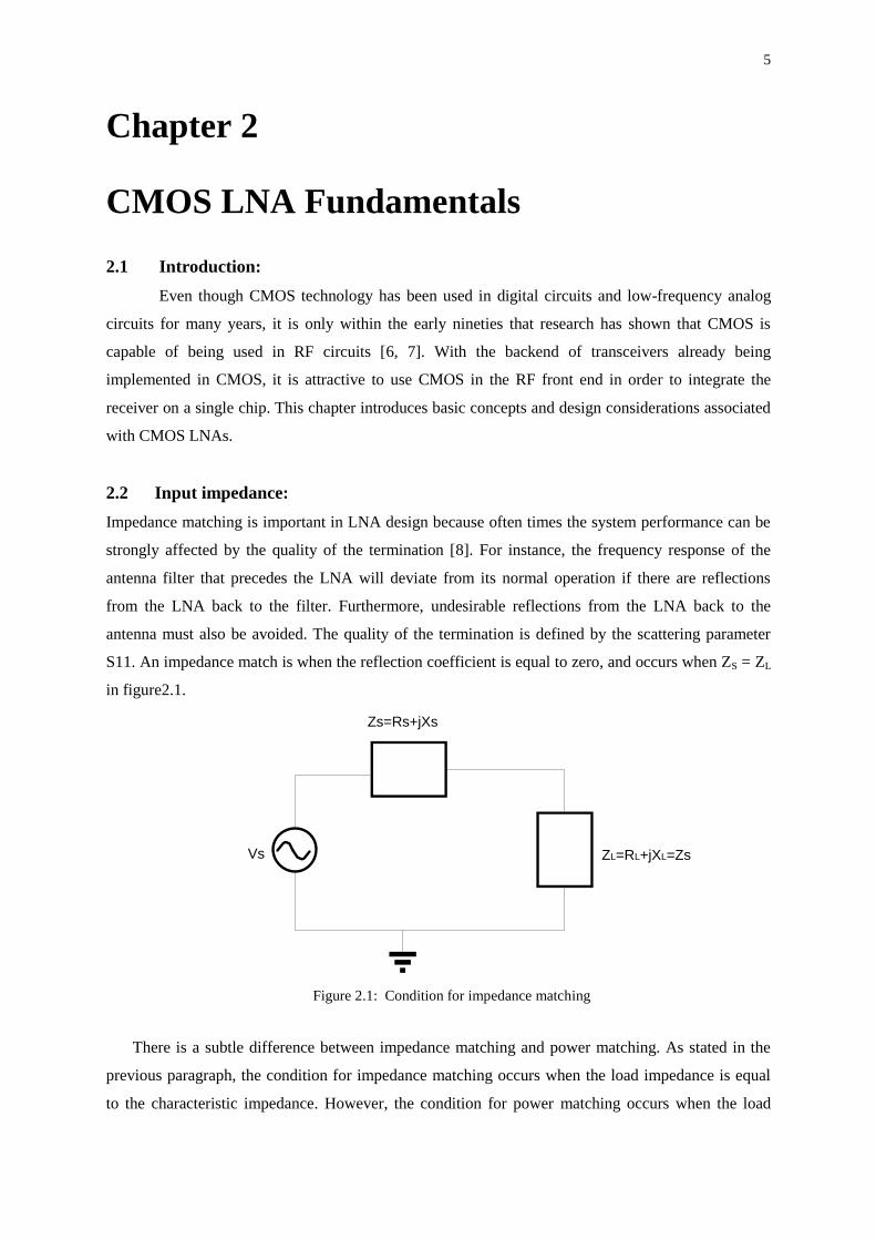
2.2 Input impedance:
Impedance matching is important in LNA design because often times the system performance can be
strongly affected by the quality of the termination [8]. For instance, the frequency response of the
antenna filter that precedes the LNA will deviate from its normal operation if there are reflections
from the LNA back to the filter. Furthermore, undesirable reflections from the LNA back to the
antenna must also be avoided. The quality of the termination is defined by the scattering parameter
S11. An impedance match is when the reflection coefficient is equal to zero, and occurs when ZS = ZL
in figure2.1.
Vs
Zs=Rs+jXs
ZL=RL+jXL=Zs
Figure 2.1: Condition for impedance matching
There is a subtle difference between impedance matching and power matching. As stated in the
previous paragraph, the condition for impedance matching occurs when the load impedance is equal
to the characteristic impedance. However, the condition for power matching occurs when the load
6
impedance is the complex conjugate of the characteristic impedance. When the impedances are real,
the conditions for power matching and impedance matching are equal.
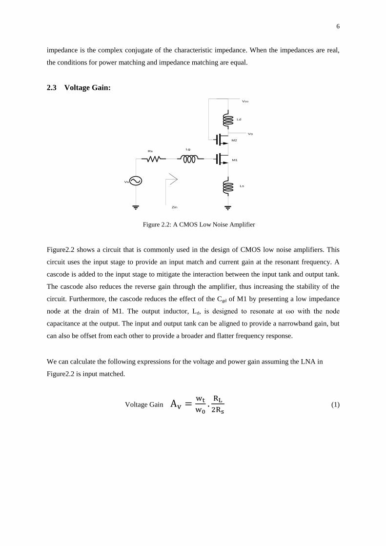
2.3 Voltage Gain:
Zin
Lg
Ls
Rs
Vs
Vo
Ld
VDD
M1
M2
Figure 2.2: A CMOS Low Noise Amplifier
Figure2.2 shows a circuit that is commonly used in the design of CMOS low noise amplifiers. This
circuit uses the input stage to provide an input match and current gain at the resonant frequency. A
cascode is added to the input stage to mitigate the interaction between the input tank and output tank.
The cascode also reduces the reverse gain through the amplifier, thus increasing the stability of the
circuit. Furthermore, the cascode reduces the effect of the Cgd of M1 by presenting a low impedance
node at the drain of M1. The output inductor, Ld, is designed to resonate at ωo with the node
capacitance at the output. The input and output tank can be aligned to provide a narrowband gain, but
can also be offset from each other to provide a broader and flatter frequency response.
We can calculate the following expressions for the voltage and power gain assuming the LNA in
Figure2.2 is input matched.
Voltage Gain
(1)

7
2.4 Inductive Source Degeneration
2.4.1 Input impedance match
It was mentioned previously that providing an impedance (and power, if the source impedance is
real) match was important in LNA design. Input impedance matching by using inductive source
degeneration is a very popular approach because matching to the source does not introduce additional
noise (as in the case of using a shunt input resistor), and does not restrict the value of gm (as in the
case of the common-gate configuration).
Zin
Lg
Ls
Rs
Vs
Figure 2.3: Inductive source degeneration
The circuit shown in figure2.3 has an input impedance equal to
(2)
Where ideal inductors have been assumed. From equation (2), in order to achieve an
Input match, the following condition must be satisfied.
Where
(3)
Where is the transition frequency of the transistor. Once Ls is chosen to provide the input match,
Lg can be chosen such that Zin is real and equal to equation (2) at the resonant frequency ωo. In other
words, the following condition for Lg must hold:
√ (4)
8
2.4.2 Effective Trans-conductance of Matched Device:
To find the trans-conductance of the circuit shown in figure2.3, first note that the input matching
network forms a series RLC tank. The Q of the tank can be defined as
(5)
Where is the resonant frequency defined in equation (4). At resonance, the voltage across the
capacitor is equal to
(6)
And the short circuit output current is equal to
(7)
Where is the intrinsic trans-conductance of the device. Using equations (5),(6) and (7), the overall
trans-conductance can be solved for, and is given by the following equation:
(
)
(8)
(9)
It can be observed from equation (9) that the effective trans-conductance is independent of the gm of
the device, and is dependent on CMOS process technology through the transition frequency.
9
Chapter 3
Transformer Coupled Input Matching for
Narrow Band LNA
A low-noise amplifier (LNA) in a wireless receiver is expected to have high gain and low noise figure
(NF) for a sufficient signal-to-noise ratio to demodulate signals. Among various MOSFET LNA
circuit topologies, the common-source (CS) based amplifier is generally preferred, as it has better
noise performance within limited power consumption. It is especially popular for extreme applications
in which ultra-low power or very high frequency is demanded. In most of the cases a cascode
transistor is added for better input-output isolation.
Main aim of the analysis of this circuit is to get deep understanding of transformer coupled input
matching technique. In general, single band LNAs are always built with narrow band LC tank circuit
as load impedance and same as input matching circuit with device parasitic. Though this circuit can
give good matching with less component count, the matching is good enough only in a narrow band.
If there is any need to tune the circuit in between a certain frequency range or multi-band gain
requirement, this kind of narrow band matching will become a bottleneck. Therefore an input
matching in a broad-band spectrum is really needed for such kind of application. Hence for better
understanding of transformer coupled matching technique, a narrow band circuit is chosen initially.
3.1 Target structure:
A critical component in an ultra-wideband (UWB) system is a wideband low-noise amplifier (LNA).
It needs to provide low noise figure, stable gain, and good input matching over the entire bandwidth
with low power consumption. Several 3−5-GHz CMOS UWB LNA topologies utilizing various input
matching networks have been reported recently such as LC band-pass filter (BPF), resistive shunt
feedback and miller effect. The BPF matching network-based topology achieves wideband
characteristics with low power consumption. However, it tends to occupy large die area due to the
need of multiple on-chip LC components. The resistive shunt feedback LNA also has wideband
characteristics, but it tends to degrade noise performance due to the feedback resistor. To further push
the performance for CMOS wideband LNA, this work explores the concept of utilizing a transformer
as a wideband input matching network which occupies small die area and provides good noise
performance [9].

10
The UWB LNA topology is shown in figure 3.1. The source degeneration inductor (Ls) is added
to realize 50Ω real impedance for input match. Where Cgs is small such that a large series inductance
at the gate of M1 is required to achieve the desired the 50Ω impedance. To resolve this issue, a
capacitor (Cd) can be added between the gate and source of M1. The input match of a cascade stage
with degeneration inductor is inherently narrowband due to the series RLC resonant circuit formed by
Ls and (Cgs+cd) in this work the transformer is utilized to absorb this series RLC circuit into a
wideband matching network.
This circuit is a simple Common Source (CS) amplifier with degenerated inductor (Ls). To
achieve high gain and good reverse isolation, a cascode stage is used in the amplifier core. The source
degeneration inductor is added to realize 50 ohms real impedance for input match. As gate-source
capacitance (Cgs) is small, an extra capacitance is added in parallel to Cgs to avoid very high value of
source inductance otherwise would be needed to realise the real impedance. Complete input matching
and gain analysis are done in this circuit. This shows a possibility of better input matching in a wide-
band and improved gain than the conventional circuit. Hence this input matching technique is
considered in concurrent dual-band LNA for improving the input matching.
Rs
L1L2
Cc
Ls
M1
M2
Rout
Lout
Cd
Vout
VDD
C1 C2
Figure 3.1 Schematic diagram of wide-band LNA
3.2 Input Matching Network:
L1 L2
Vin I1
I2
I2
Cc
C1
CtRt
Ls
Rs
Zin
V2
ZtZy
Figure 3.2 Equivalent circuit for input matching
Figure 3.2 shows the simplified equivalent circuit for the proposed transformer-based input
matching network.
11
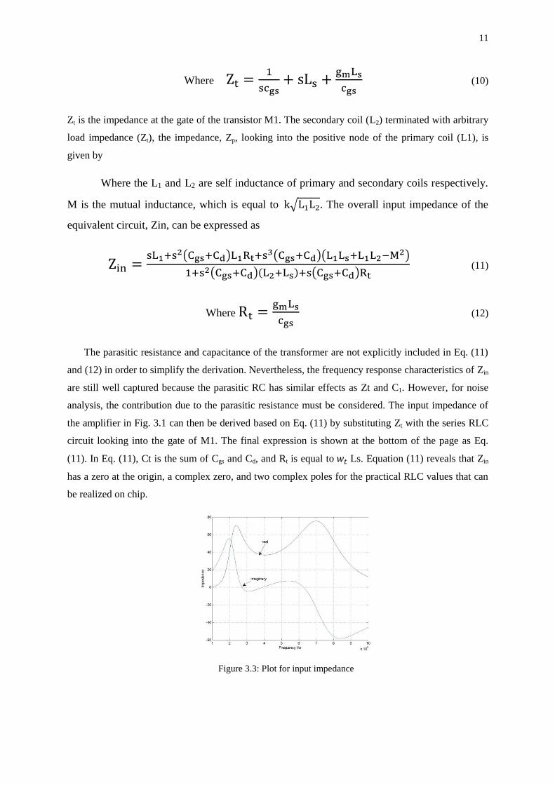
Where
(10)
Zt is the impedance at the gate of the transistor M1. The secondary coil (L2) terminated with arbitrary
load impedance (Zt), the impedance, Zp, looking into the positive node of the primary coil (L1), is
given by
Where the L1 and L2 are self inductance of primary and secondary coils respectively.
M is the mutual inductance, which is equal to √ . The overall input impedance of the
equivalent circuit, Zin, can be expressed as
( ) ( )( )
( ) ( ) (11)
Where
(12)
The parasitic resistance and capacitance of the transformer are not explicitly included in Eq. (11)
and (12) in order to simplify the derivation. Nevertheless, the frequency response characteristics of Zin
are still well captured because the parasitic RC has similar effects as Zt and C1. However, for noise
analysis, the contribution due to the parasitic resistance must be considered. The input impedance of
the amplifier in Fig. 3.1 can then be derived based on Eq. (11) by substituting Zt with the series RLC
circuit looking into the gate of M1. The final expression is shown at the bottom of the page as Eq.
(11). In Eq. (11), Ct is the sum of Cgs and Cd, and Rt is equal to Ls. Equation (11) reveals that Zin
has a zero at the origin, a complex zero, and two complex poles for the practical RLC values that can
be realized on chip.
Figure 3.3: Plot for input impedance

12
3.3 Output stage:
To achieve high gain under low voltage headroom, an inductor with a series resistor is
adopted as the output load to implement a low-Q, tuned load to cover the desired bandwidth.
Rout
Lout
CoutZload
Figure 3.4: Equivalent circuit for output impedance
The output impedance Zload, can be expressed as
(13)
Where Cout is the total output capacitance at the drain node of M2. A source follower buffer
stage with a current source load is added at the output to drive an off-chip 50-Ω load during testing.
3.4 Gain calculation
The proposed amplifier can be divided into two parts to derive its voltage gain: the input matching
network and the cascode stage with an inductive load. The transfer function of the input matching
network is
√
( ( ) )
(14)
Where vgs1 is the voltage across the gate and source nodes of M1. Because the output voltage at
the drain of M2 is gm1 vgs1 Zload, the overall voltage gain of the amplifier shown in Fig. 3.1 can be
calculated by
(15)
Ain is the voltage gain between Vs and Vin as defined in Fig. 3.1 and can be found as follows.
(16)
13
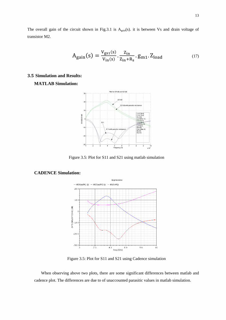
The overall gain of the circuit shown in Fig.3.1 is Again(s). it is between Vs and drain voltage of
transistor M2.
(17)
3.5 Simulation and Results:
MATLAB Simulation:
Figure 3.5: Plot for S11 and S21 using matlab simulation
CADENCE Simulation:
Figure 3.5: Plot for S11 and S21 using Cadence simulation
When observing above two plots, there are some significant differences between matlab and
cadence plot. The differences are due to of unaccounted parasitic values in matlab simulation.
14
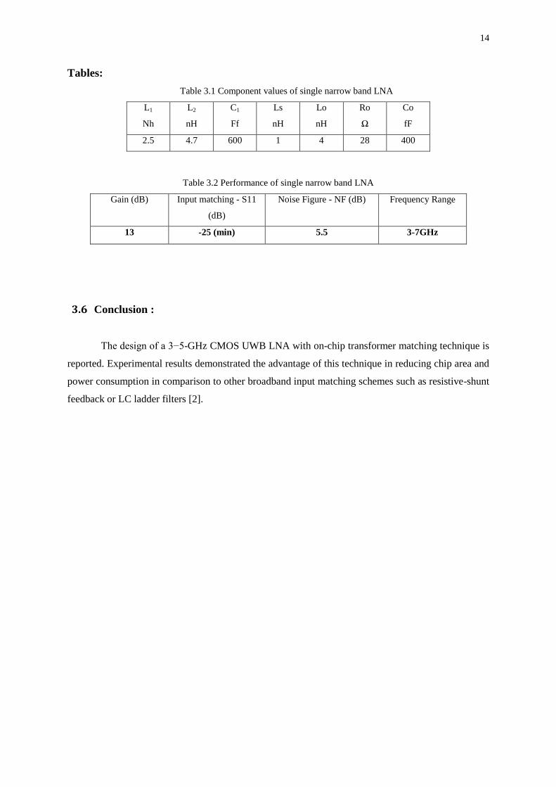
Tables:
Table 3.1 Component values of single narrow band LNA
L1
Nh
L2
nH
C1
Ff
Ls
nH
Lo
nH
Ro
Ω
Co
fF
2.5 4.7 600 1 4 28 400
Table 3.2 Performance of single narrow band LNA
Gain (dB) Input matching - S11
(dB)
Noise Figure - NF (dB) Frequency Range
13 -25 (min) 5.5 3-7GHz
3.6 Conclusion :
The design of a 3−5-GHz CMOS UWB LNA with on-chip transformer matching technique is
reported. Experimental results demonstrated the advantage of this technique in reducing chip area and
power consumption in comparison to other broadband input matching schemes such as resistive-shunt
feedback or LC ladder filters [2].

15
Chapter 4
Concurrent Dual-Band LNA
4.1 Introduction:
Standard receiver architectures, such as super heterodyne and direct conversion, accomplish
high selectivity and sensitivity by narrow-band operation at a single RF frequency. These modes of
operation limit the system’s available bandwidth and robustness to channel variations and thus its
functionality. On the other hand, wideband modes of operation are more sensitive to out-of-band
signals due to transistor non-linearity, which can introduce severe bottlenecks in system performance.
The diverse range of modern wireless applications necessitates communication systems with more
bandwidth and flexibility. More recently, dual-band transceivers have been introduced to increase
the functionality of such communication systems by switching between two different bands and
receive one band at a time. While switching between bands improves receiver’s versatility (e.g.,
in dual-band cellular phones), it is not sufficient in the case of a multi-functionality transceiver
(e.g., a cellular phone with a GPS receiver and a Bluetooth interface). Using conventional receiver
architectures, simultaneous operation at different frequencies can only be achieved by building
multiple independent signal paths with an inevitable increase in the cost, footprint and power
dissipation. In this work, new concurrent dual-band receiver architecture is introduced that is capable
of simultaneous operation at two different frequencies without dissipating twice as much power or a
significant increase in cost and footprint. This concurrent operation can be used to extend the
available bandwidth, provide new functionality and/or add diversity to battle channel fading. The
concurrent operation is realized through an elaborate frequency conversion scheme, in conjunction
with a novel concurrent dual-band low noise amplifier (LNA). These new concurrent multi-band
LNAs provide simultaneous narrowband gain and matching at multiple frequency bands.
In conventional dual-band single-chip receivers, each signal path is allocated for each frequency
band. A single-band LNAs is selected according to the operation band, which results in a high
implementation coast due to the large chip area as well as high static power consumption due to
multiple bias paths. Another method is to accommodate wide-band LNA. Unfortunately, in a
wideband LNA, strong unwanted blockers are amplified together with the desired frequency bands
and significantly degrade the receiver sensitivity. To overcome this area, power and other issues,
concurrent multi-band LNAs are always preferred. These LNAs are simple in architecture and work
simultaneously on both the bands with reduced power consumption and better area efficiency.
16
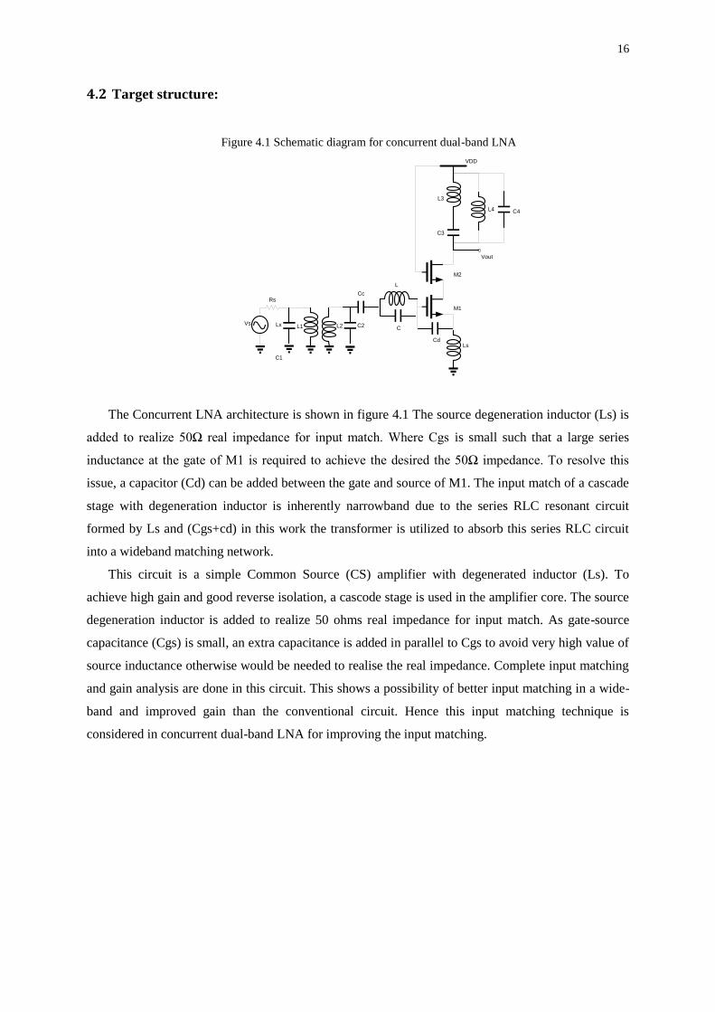
4.2 Target structure:
Figure 4.1 Schematic diagram for concurrent dual-band LNA
Vs
Cc
Ls
M1
M2
Vout
VDD
C2
L3
L4
C3
C4
Cd
Rs
L1 L2
C1
Lx
L
C
The Concurrent LNA architecture is shown in figure 4.1 The source degeneration inductor (Ls) is
added to realize 50Ω real impedance for input match. Where Cgs is small such that a large series
inductance at the gate of M1 is required to achieve the desired the 50Ω impedance. To resolve this
issue, a capacitor (Cd) can be added between the gate and source of M1. The input match of a cascade
stage with degeneration inductor is inherently narrowband due to the series RLC resonant circuit
formed by Ls and (Cgs+cd) in this work the transformer is utilized to absorb this series RLC circuit
into a wideband matching network.
This circuit is a simple Common Source (CS) amplifier with degenerated inductor (Ls). To
achieve high gain and good reverse isolation, a cascode stage is used in the amplifier core. The source
degeneration inductor is added to realize 50 ohms real impedance for input match. As gate-source
capacitance (Cgs) is small, an extra capacitance is added in parallel to Cgs to avoid very high value of
source inductance otherwise would be needed to realise the real impedance. Complete input matching
and gain analysis are done in this circuit. This shows a possibility of better input matching in a wide-
band and improved gain than the conventional circuit. Hence this input matching technique is
considered in concurrent dual-band LNA for improving the input matching.
17
4.3 Input matching:
L1 L2
Vin I1
I2
I2
L
C
Cc
C1C2
Zlc
CtRt
Ls
VgsRs
Vs
Zin
V2
ZtZwZxZy
Figure 4.2 Equivalent circuit for input impedance
Figure.4.2 simplified equivalent circuit of transformer based input matching network
Therefore the overall impedance of the circuit is
(18)
Where
(19)
(20)
(21)
4.4 Output stage:
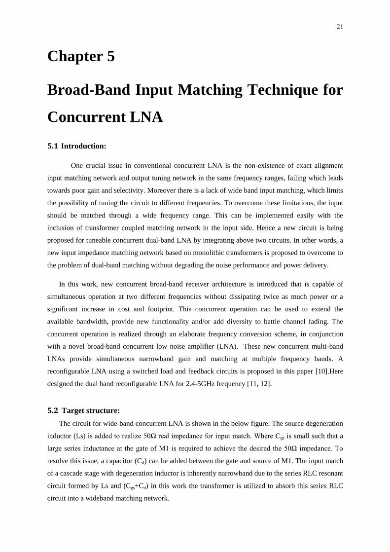
In order to achieve narrow-band gain at bands of interest, the drain load network should
exhibit high impedance only at those frequencies. This can be done by adding a series LC
branch in parallel with the parallel LC tank of a single-band LNA, as shown in Fig .
Each series LC branch introduces a zero in the gain transfer function of the LNA at its
series resonant frequency. The frequencies of the zeros determine the frequency of the
notches in the transfer function, which are used to greatly enhance the image rejection of the
receiver.

18
L3
L4
C3
C4
Zout
Figure 4.3 Equivalent circuit for output impedance
(22)
4.5 Gain:
The proposed amplifier can be divided into two parts to derive its voltage gain: the input matching
network and the cascode stage with an inductive load. The transfer function of the input matching
network is
√
(23)
Where vgs1 is the voltage across the gate and source nodes of M1. Because the output voltage at the
drain of M2 is gm1 vgs1 Zload, the overall voltage gain of the amplifier shown in Fig. 4.1 can be
calculated by
(24)
Ain is the voltage gain between Vs and Vgs1 as defined in Fig. 4.2 and can be found as follows.
(25)
The overall gain of the circuit shown in fig.4.1 is Again(s). it is between Vs and drain voltage of
transistor M2.
(26)

19
4.6 Simulations and Results:
CADENCE Simulation
Figure 4.4 Plot for S11,S21 and Noise figure using Cadence simulation
Matlab simulation
Figure 4.4 Plot for S11 and S21 using Matlab simulation
20
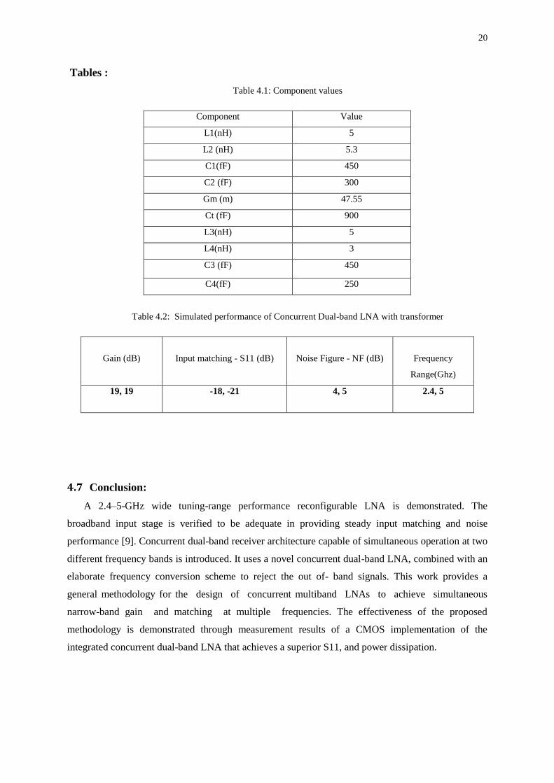
Tables :
Table 4.1: Component values
Component Value
L1(nH) 5
L2 (nH) 5.3
C1(fF) 450
C2 (fF) 300
Gm (m) 47.55
Ct (fF) 900
L3(nH) 5
L4(nH) 3
C3 (fF) 450
C4(fF) 250
Table 4.2: Simulated performance of Concurrent Dual-band LNA with transformer
Gain (dB)
Input matching - S11 (dB)
Noise Figure - NF (dB)
Frequency
Range(Ghz)
19, 19 -18, -21 4, 5 2.4, 5
4.7 Conclusion:
A 2.4–5-GHz wide tuning-range performance reconfigurable LNA is demonstrated. The
broadband input stage is verified to be adequate in providing steady input matching and noise
performance [9]. Concurrent dual-band receiver architecture capable of simultaneous operation at two
different frequency bands is introduced. It uses a novel concurrent dual-band LNA, combined with an
elaborate frequency conversion scheme to reject the out of- band signals. This work provides a
general methodology for the design of concurrent multiband LNAs to achieve simultaneous
narrow-band gain and matching at multiple frequencies. The effectiveness of the proposed
methodology is demonstrated through measurement results of a CMOS implementation of the
integrated concurrent dual-band LNA that achieves a superior S11, and power dissipation.
21
Chapter 5
Broad-Band Input Matching Technique for
Concurrent LNA
5.1 Introduction:
One crucial issue in conventional concurrent LNA is the non-existence of exact alignment
input matching network and output tuning network in the same frequency ranges, failing which leads
towards poor gain and selectivity. Moreover there is a lack of wide band input matching, which limits
the possibility of tuning the circuit to different frequencies. To overcome these limitations, the input
should be matched through a wide frequency range. This can be implemented easily with the
inclusion of transformer coupled matching network in the input side. Hence a new circuit is being
proposed for tuneable concurrent dual-band LNA by integrating above two circuits. In other words, a
new input impedance matching network based on monolithic transformers is proposed to overcome to
the problem of dual-band matching without degrading the noise performance and power delivery.
In this work, new concurrent broad-band receiver architecture is introduced that is capable of
simultaneous operation at two different frequencies without dissipating twice as much power or a
significant increase in cost and footprint. This concurrent operation can be used to extend the
available bandwidth, provide new functionality and/or add diversity to battle channel fading. The
concurrent operation is realized through an elaborate frequency conversion scheme, in conjunction
with a novel broad-band concurrent low noise amplifier (LNA). These new concurrent multi-band
LNAs provide simultaneous narrowband gain and matching at multiple frequency bands. A
reconfigurable LNA using a switched load and feedback circuits is proposed in this paper [10].Here
designed the dual band reconfigurable LNA for 2.4-5GHz frequency [11, 12].
5.2 Target structure:
The circuit for wide-band concurrent LNA is shown in the below figure. The source degeneration
inductor (Ls) is added to realize 50Ω real impedance for input match. Where Cgs is small such that a
large series inductance at the gate of M1 is required to achieve the desired the 50Ω impedance. To
resolve this issue, a capacitor (Cd) can be added between the gate and source of M1. The input match
of a cascade stage with degeneration inductor is inherently narrowband due to the series RLC resonant
circuit formed by Ls and (Cgs+Cd) in this work the transformer is utilized to absorb this series RLC
circuit into a wideband matching network.

22
This circuit is a Common Source (CS) amplifier with degenerated inductor (Ls). To achieve high
gain and good reverse isolation, a cascode stage is used in the amplifier core. The source degeneration
inductor is added to realize 50 ohms real impedance for input match. As gate-source capacitance
(Cgs) is small, an extra capacitance is added in parallel to Cgs to avoid very high value of source
inductance otherwise would be needed to realise the real impedance. Complete input matching and
gain analysis are done in this circuit. This shows a possibility of better input matching in a wide-band
and improved gain than the conventional circuit.
Vs
Rs
L1 L2
Cc
Ls
M1
M2
Vout
VDD
C1 C2
L3
L4
C3
C4
Cd
Figure 5.1: Schematic diagram of broad-band matched concurrent LNA
5.3 Input stage:
Figure 5.2 shows the simplified equivalent circuit for the proposed transformer-based input
matching network.
L1 L2Zt
Vin
I1
I2
I2
Zin
Figure 5.2 Equivalent circuit diagram for input impedance

23
Where
(27)
Zt is the impedance at the gate of the transistor M1. The secondary coil (L2) terminated with arbitrary
load impedance (Zt), the impedance, Zp, looking into the positive node of the primary coil (L1), is
given by
Where L1 and L2 are the self inductance of the primary and secondary coil, respectively. M is
the mutual inductance, which is equal to √ . The overall input impedance of the equivalent
circuit, Zin, can be expressed as
( ) ( )( )
( ) ( ) (28)
Where
(29)
The parasitic resistance and capacitance of the transformer are not explicitly included in Eq. (28)
and (29) in order to simplify the derivation. Nevertheless, the frequency response characteristics of Zin
are still well captured because the parasitic RC has similar effects as Zt and C1. However, for noise
analysis, the contribution due to the parasitic resistance must be considered. The input impedance of
the amplifier in Fig. 1 can then be derived based on Eq. (28) by substituting Zt with the series RLC
circuit looking into the gate of M1. The final expression is shown of the page as Eq. (28). In Eq. (28),
Ct is the sum of Cgs and Cd, and Rt is equal to ωT Ls. Equation (28) reveals that Zin has a zero at the
origin, a complex zero, and two complex poles for the practical RLC values that can be realized on
chip.
Frequencies whose values can be solved numerically using Matlab. For the targeted bandwidth of
2–7 GHz, the complex zero is set to 4 GHz, and the two complex poles are placed at 2.5 and 7 GHz as
shown in Fig. The corresponding S11 is shown in Fig. 5.1. For design margin, the bandwidth of the
input match is designed to be from 2–6 GHz.
5.4 Output stage:
24
In order to achieve narrow-band gain at bands of interest, the drain load network should
exhibit high impedance only at those frequencies. This can be done by adding a series LC branch in
parallel with the parallel LC tank of a single-band LNA, as shown in Fig . Each series LC
branch introduces a zero in the gain transfer function of the LNA at its series resonant
frequency. The frequencies of the zeros determine the frequency of the notches in the transfer
function, which are used to greatly enhance the image rejection of the receiver.
L3
L4
C3
C4
Zout
Figure 5.3 Equivalent circuit for output impedance
(30)
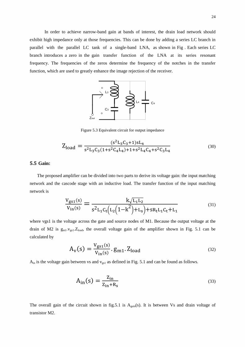
5.5 Gain:
The proposed amplifier can be divided into two parts to derive its voltage gain: the input matching
network and the cascode stage with an inductive load. The transfer function of the input matching
network is
√
( ( ) )
(31)
where vgs1 is the voltage across the gate and source nodes of M1. Because the output voltage at the
drain of M2 is gm1.vgs1.Zload, the overall voltage gain of the amplifier shown in Fig. 5.1 can be
calculated by
(32)
Ain is the voltage gain between vs and vgs1 as defined in Fig. 5.1 and can be found as follows.
(33)
The overall gain of the circuit shown in fig.5.1 is Again(s). It is between Vs and drain voltage of
transistor M2.

25
(34)
5.6 Simulation and results:
Figure 5.4 Plot for S11 and S21 using Matlab simulation
Figure 5.5 Plot for S11 and S21 using Cadence simulation
5.7 Tunable Dual-band LNA
The tuned results of above broad LNA is shown in the below plots. Where the bands of LNA can
be tune to required frequencies by switching the capacitances of the output network.

26
Figure 5.6: Tuned Dual-band LNA with Concurrent matching (C3 is variable)
Figure 5.7: Tuned Dual-band LNA with Concurrent matching (C4 is variable)
Where we can observe that fading in each band is limited by bandwidth of input matching and the
number of bands. As increasing the number bands in the output network, fading in each band will
reduce.
27
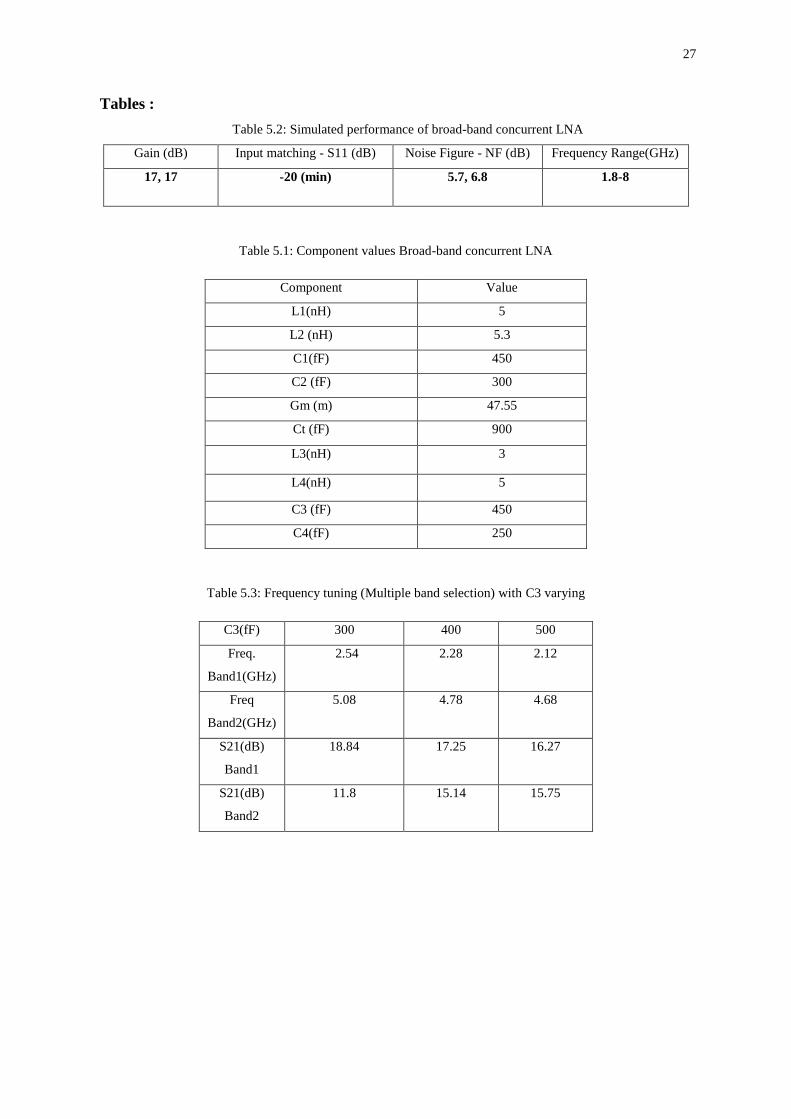
Tables :
Table 5.2: Simulated performance of broad-band concurrent LNA
Gain (dB) Input matching - S11 (dB) Noise Figure - NF (dB) Frequency Range(GHz)
17, 17 -20 (min) 5.7, 6.8 1.8-8
Table 5.1: Component values Broad-band concurrent LNA
Component Value
L1(nH) 5
L2 (nH) 5.3
C1(fF) 450
C2 (fF) 300
Gm (m) 47.55
Ct (fF) 900
L3(nH) 3
L4(nH) 5
C3 (fF) 450
C4(fF) 250
Table 5.3: Frequency tuning (Multiple band selection) with C3 varying
C3(fF) 300 400 500
Freq.
Band1(GHz)
2.54 2.28 2.12
Freq
Band2(GHz)
5.08 4.78 4.68
S21(dB)
Band1
18.84 17.25 16.27
S21(dB)
Band2
11.8 15.14 15.75
28
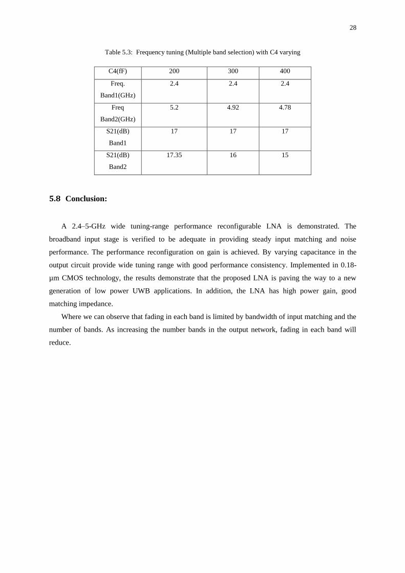
Table 5.3: Frequency tuning (Multiple band selection) with C4 varying
C4(fF) 200 300 400
Freq.
Band1(GHz)
2.4 2.4 2.4
Freq
Band2(GHz)
5.2 4.92 4.78
S21(dB)
Band1
17 17 17
S21(dB)
Band2
17.35 16 15
5.8 Conclusion:
A 2.4–5-GHz wide tuning-range performance reconfigurable LNA is demonstrated. The
broadband input stage is verified to be adequate in providing steady input matching and noise
performance. The performance reconfiguration on gain is achieved. By varying capacitance in the
output circuit provide wide tuning range with good performance consistency. Implemented in 0.18-
µm CMOS technology, the results demonstrate that the proposed LNA is paving the way to a new
generation of low power UWB applications. In addition, the LNA has high power gain, good
matching impedance.
Where we can observe that fading in each band is limited by bandwidth of input matching and the
number of bands. As increasing the number bands in the output network, fading in each band will
reduce.

29
Chapter 6
Conclusion and Future Work
6.1 Conclusion
The possibility of integrating transformer coupling on input matching network of concurrent dual-
band LNA is analyzed. Performance of narrow band LNA with transformer coupled input matching
and LC matched concurrent LNA were also analyzed for verification. When compared to LC matched
concurrent LNA, this transformer coupling technique provides better matching in a wide-band
scenario. Though this wide-band matching may not prevent out of band signals perfectly, this will be
very much useful in designing tunable concurrent dual-band LNA.
6.2 Future Work
A tune able concurrent dual-band LNA can be designed. The design can use wide-band input
matching with transformer coupled technique. This will be the future development of this work.

30
References
[1] Hossein Hashemi and Ali Hajimiri, “Concurrent Dual-Band CMOS Low Noise Amplifiers and
Receiver Architectures”, Symposium on VLSI Circuits, 2001.
[2] Dong Hun Shin, Jaejin Park and C. Patrick Yue , “A Low-Power, 3–5-GHz CMOS UWB LNA
Using Transformer Matching Technique”, IEEE Asia Solid State Conference, Korea, Nov-2007.
[3] Ouail EL-Gharniti, Eric Kerhervé, Jean-Baptiste Bégueret and Didier Belot, “Concurrent Dual-
Band Low Noise Amplifier for 802.11a/g WLAN applications”, IEEE 15th International
conference (ICECS), Canada, Dec 2006, page(s): 66 – 69.
[4] Sambit Datta, Ashudeb Dutta and Tarnn Kanti Bhattacharyya, “A Gain Boosted Fully Concurrent
Dual-Band Interstage Matched LNA Operating in 900 MHz2.4 GHz with sub-2dB Noise Figure”,
ICCCT, Jan-2010.
[5] Xinzhong Duo, Li-Rong Zheng, Mohammed Ismail and Hannu Tenhunen, “A Concurrent Multi-
Band LNA for Multi-Standard Radios”, IEEE international symposium, Japan, May 2005,
pages: 3982 - 3985 Vol. 4.
[6] D. Shaeffer, T. Lee, “A 1.5 V, 1.5 GHz CMOS low noise amplifier,” IEEE Journal of Solid State
Circuits, Vol. 32, May 1997.
[7] J. Ou. “CMOS RF Device Modeling and Low-Noise Amplifier Circuit Design,” Ph.D Thesis -
University of California, Berkeley, Berkeley, CA 2001.
[8] J. Janssens, M. Steyaert. “CMOS Cellular Receiver Front-Ends. Klewer”, The Netherlands, 2002.
[9] Chang-Tsung Fu, Chun-Lin Ko, Chien-Nan Kuo, Ying-Zong Juang, “A 2.4–5.4-GHz Wide
Tuning-Range CMOS Reconfigurable Low-Noise Amplifier” IEEE Transactions on Microwave
Theory and Techniques, vol.56, no.12, Dec 2008.
[10] Vu Kien Dao, Quang Diep Bui and Chul Soon Park, “A Multi-band 900MHz/1.8GHz/5.2GHz
LNA for Reconfigurable Radio” IEEE Radio Frequency Integrated Circuits Symposium, Hawaii.
June 2007, Page(s): 69 – 72.
[11] Si Xiong, Yumei Huang, Zhiliang Hon, “A Dual-Band 2.1GHz/5.2GHz LNA for Reconfigurable
Radio”, Solid-State and Integrated Circuit Technology (ICSICT), 2010 10th IEEE International
Conference, Greece, page(s): 710 – 712.

31
[12] Santosh Kumar Gupta, Abhash Garg, Nitin Prabhakar Singh, “Design and Simulation of an
improved Dual Band LNA for WLAN Applications”, ICCCT 2010, India, Page(s): 678 – 682.
[13] T. H. Lee, “The Design of CMOS Radio-Frequency Integrated Circuits”, 2nd
ed., Cambridge
University Press, 2004.
[14] Behzad Razavi, “RF Microelectronics”, Prentice Hall PTR, NJ, 1997.