analysis, construction and evaluation of a radial...
TRANSCRIPT
Department of Microtechnology and Nanoscience CHALMERS UNIVERSITY OF TECHNOLOGY Gothenburg, Sweden 2017
Analysis, Construction and Evaluation
of a Radial Power Divider/Combiner
Design of an 8-way TM020 Radial Cavity Divider/
Combiner with Coaxial Ports
Master’s Thesis in Wireless, Photonics and Space Engineering
IDA KLÄPPEVIK


Analysis, Construction and Evaluation of a Radial Power
Divider/Combiner
IDA KLÄPPEVIK
Department of Microtechnology and Nanoscience
Microwave Electronics Laboratory
Chalmers University of Technology
Gothenburg, Sweden 2017

iv
Analysis, Construction and Evaluation of a Radial Power Divider/Combiner
IDA KLÄPPEVIK
© IDA KLÄPPEVIK, 2017.
Supervisor: Magnus Isacsson, Saab Surveillance
Examiner: Dan Kuylenstierna, Chalmers University of Technology, Microtechnology and
Nanoscience
Department of Microtechnology and Nanoscience
Microwave Electronics Laboratory
Chalmers University of Technology
SE-412 96 Gothenburg
Telephone +46 31 772 1000
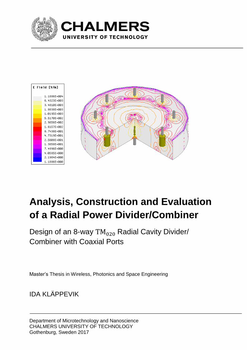
Cover: Cross section of the simulated electromagnetic field within a passive combiner/divider
structure based on a resonant, cylindrical cavity, where coaxial probes excite the TM020 mode.
The centred port at the bottom of the cavity is excited with 1 W.
Gothenburg, Sweden 2017

v
vi
Analysis, Construction and Evaluation of a Radial Power Divider/Combiner
IDA KLÄPPEVIK
Department of Microtechnology and Nanoscience
Chalmers University of Technology
ABSTRACT
Radial N-way combiners and dividers are efficient and compact structures for power
combining and dividing, which combines or divides the power of N inputs in one single step.
The use of this method results in low losses and therefore presents an interesting alternative to
often used combiner and divider networks, such as binary tree structures consisting of 2- or 3-
way splitters.
In this thesis project, the construction of radial N-way cavity combiners and dividers is
analysed and an 8-port TM020 cylindrical cavity combiner/divider with SMA-connector input
and output ports is designed and fabricated. The characteristics of the fabricated prototype is
evaluated and compared to the simulated design. The average return loss at the peripheral
ports is higher than 18.4 dB and the return loss at the centre port is higher than 17.6 dB for a
10 % bandwidth around the centre design frequency of 3.1 GHz. The measured insertion loss
is lower than 0.16 dB for the same band.
The divider and combiner are used in an active test setup with 8 InGaP HBT amplifiers, by
which a study of degradation in the event of amplifier failure is performed. Methods to reach
a more graceful degradation are discussed. The thesis report also presents a brief overview of
different types of N-way combiners and a comparison between the characteristics of some
published designs.
In conclusion, radial N-way combiners are a very attractive alternative for combining in high
power systems due to their low-loss performance and the gradual loss of power in the event of
amplifier failure. If they are used together with solid state power amplifiers, they can be used
to replace other high power RF amplifier solutions such as the travelling wave tube amplifier.
Keywords: Power combining, cavity combiner, graceful degradation, N-way combiner, power
combiner, power divider

vii

viii
PREFACE
In this thesis project, the concept of radial cavity power combiners has been investigated
through theoretical studies and practical experiments. The thesis work resulted in two
fabricated structures that were designed for power combining and dividing, and their
functionality was tested and compared to simulated results.
The thesis project was carried out at Saab AB, with Magnus Isacsson (Saab AB) as supervisor
and Dan Kuylenstierna (Chalmers University of Technology) as examiner. The work took
place at Chalmers University of Technology and Saab AB from November 2016 to May 2017.
Firstly, I would like to express my sincere gratitude to my supervisor Magnus Isacsson for his
dedicated supervision of this project, and for providing me with an introduction to practical
engineering. Secondly, I would like to thank my examiner Dan Kuylenstierna for the guidance
regarding the planning of the thesis project and the project report. I would also like to thank
Niklas Einvall at Saab AB who made this thesis project possible.
Finally, I am very grateful towards the help and support from Theofilos Markopoulos, Sofia
Berg, Ludvig Magnusson, Andreas Wikström, Per Agesund, Per Aulin, Sigrid Hammarqvist
and other colleagues at Saab and all of my fellow thesis worker colleagues.
Ida Kläppevik, Gothenburg, May 2017

ix

x
TABLE OF CONTENTS
LIST OF FIGURES ................................................................................................................. xiii
LIST OF TABLES ................................................................................................................ xviii
1 INTRODUCTION .............................................................................................................. 1
1.1 Aim of the project ........................................................................................................ 1
1.2 Demarcations ............................................................................................................... 2
2 THEORY ............................................................................................................................ 3
2.1 Cylindrical Cavity Resonators ..................................................................................... 3
2.1.1 Electromagnetic Fields in Cylindrical Cavities .................................................... 4
2.1.2 Resonant Modes ................................................................................................... 5
2.1.3 Q-factor of Resonators ......................................................................................... 6
2.1.4 The Scattering Matrix for Microwave Networks ................................................. 7
2.1.5 Impedance of Cavity Resonators .......................................................................... 8
2.1.6 Excitation of Cavities ........................................................................................... 9
2.2 Power Dividing/Combining ....................................................................................... 10
2.2.1 N-port Power Combining ................................................................................... 10
2.2.2 Power Combining Techniques ........................................................................... 11
2.3 Methods of Realization of Radial N-way Combiners ................................................ 12
2.3.1 Radial Cavity-Based Combiners ........................................................................ 13
2.3.2 Radial Non-Cavity-Based Combiners ................................................................ 16
2.3.3 Spatial Combiners .............................................................................................. 16
3 DIVIDER AND COMBINER DESIGN AND FABRICATION ..................................... 18
3.1 Conceptual Study of Cylindrical Cavity Dividers and Combiners ............................ 18
3.1.1 Cylindrical Cavity .............................................................................................. 18
3.1.2 Position and Choice of Peripheral and Centre Ports .......................................... 20
3.1.3 Impedance Matching .......................................................................................... 22
3.1.4 Bandwidth .......................................................................................................... 26
3.1.5 Isolation .............................................................................................................. 26
3.2 Design Requirements for Prototype Divider and Combiner...................................... 27
3.2.1 Amplifier ............................................................................................................ 27
3.2.2 Central and Peripheral Ports ............................................................................... 27
3.2.3 Number of Ports ................................................................................................. 27
3.2.4 Bandwidth .......................................................................................................... 27
xi
3.2.5 Isolation .............................................................................................................. 28
3.3 8-port Cylindrical Cavity Divider and Combiner Prototype ..................................... 28
3.3.1 Design of Cylindrical Cavity .............................................................................. 28
3.3.2 Peripheral and Centre Ports ................................................................................ 28
3.3.3 Impedance Matching by Connector Modification ............................................. 30
3.3.4 Measurements of Final Design ........................................................................... 34
3.4 Fabrication of Prototype and Test Setup ................................................................... 36
3.4.1 Fabrication Considerations of Divider and Combiner ....................................... 36
3.4.2 Fabrication of SMA Connector Probe Modifications ........................................ 38
4 SIMULATED AND MEASURED PERFORMANCE .................................................... 39
4.1 Comparison of the Fabricated Structures and the Simulated Model ......................... 39
4.1.1 Scattering parameters ......................................................................................... 40
4.1.2 Return and Insertion Loss .................................................................................. 42
4.1.3 Leakage and Isolation ......................................................................................... 43
4.1.4 Sensitivity for Phase and Amplitude Variations ................................................ 45
4.2 Characteristics of Divider Connected to Combiner ................................................... 46
4.2.1 Scattering Parameters ......................................................................................... 47
4.2.2 Return and Insertion Losses ............................................................................... 48
4.2.3 Broaband Filter Characteristics .......................................................................... 49
4.3 Test Setup with Solid State Power Amplifiers .......................................................... 50
4.3.1 Graceful Degradation in the Event of Amplifier Failure ................................... 51
4.3.2 Methods for Improvement of Graceful Degradation .......................................... 54
5 DISCUSSION AND FURTHER WORK ......................................................................... 57
5.1 Radial Power Combiner as an Alternative for Combiner Networks ......................... 57
5.2 Construction of Radial Cavity Power Combiners in General .................................... 57
5.3 Evaluation of the Design, Fabrication and Verification of the 8-Way Cavity
Combiner/Divider Structures ................................................................................................ 57
5.4 Recommended Future Work ...................................................................................... 58
5.5 Ethical Aspects and a Sustainability Perspective of the Radial Power
Combiner/Divider ................................................................................................................. 58
6 CONCLUSION ................................................................................................................. 60
BIBLIOGRAPHY .................................................................................................................... 61
Calculation of Resonator Impedance ............................................................. I APPENDIX A
Equivalent Circuit of Slits and Diaphragms in Waveguide-to-Cavity Ports II APPENDIX B

xii
Combiner Waveguide Output ..................................................................... III APPENDIX C
xiii
LIST OF FIGURES Figure 2-1. Schematic picture of a resonant cylindrical cavity with examples of resonant
waves shown in height and radial dimensions. .......................................................................... 3
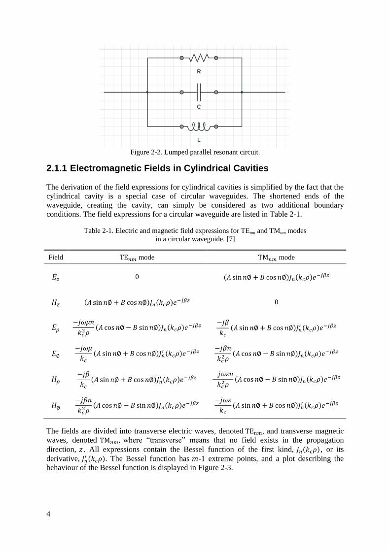
Figure 2-2. Lumped parallel resonant circuit. ............................................................................ 4
Figure 2-3. The behaviour of the Bessel function of first kind. ................................................. 5
Figure 2-4. Schematic display of power combining/dividing. ................................................. 11
Figure 2-5. Schematic display of binary tree structure with 3 steps and 23
= 8 solid state power
amplifiers. ................................................................................................................................. 12
Figure 2-6. Different N-port power combining techniques arranged in a tree structure. ......... 13
Figure 3-1. Resonant modes in the cylindrical cavity calculated from the solutions to the
Bessel function from Table 2-2. Some of the modes overlap. The resonant modes closest to
TM020 are TM210 and TE120. ...................................................................................................... 19
Figure 3-2. Normalized real (resistive) and imaginary (reactive) impedance variation with
height for aTM020 cylindrical cavity combiner......................................................................... 20
Figure 3-3. Reflection and transmission scattering parameter for a cylindrical cavity with two
symmetric centre ports positioned opposite to each other. The cavity height is varied between
three different heights: 31.5 mm, 34 mm and 36.5 mm. .......................................................... 20
Figure 3-4. Three conceptual cavity combiner designs with waveguide ports: a) 4-port cavity
structure, b) 6-port cavity structure and c) 8-port cavity structure. .......................................... 21
Figure 3-5. Equivalent circuit of an N-port combiner structure. .............................................. 22
Figure 3-6. Addition of metallic obstacles (red) to the 4-port design; a) horizontal slabs and c)
output aperture iris. .................................................................................................................. 23
Figure 3-7. An outward shift of the peripheral waveguides in the radial direction creates a
metallic obstacle (red) in the junction between the cavity and the waveguides....................... 23
Figure 3-8. The peripheral ports are numbered 1 to N (counter clockwise), and the centre port
is numbered N+1. ..................................................................................................................... 23
Figure 3-9. Simulated effect of impedance alternation performed with slits and diaphragms in
the aperture junction between the cylindrical cavity and the peripheral rectangular waveguides
for the 4-port structure. ............................................................................................................. 24

xiv
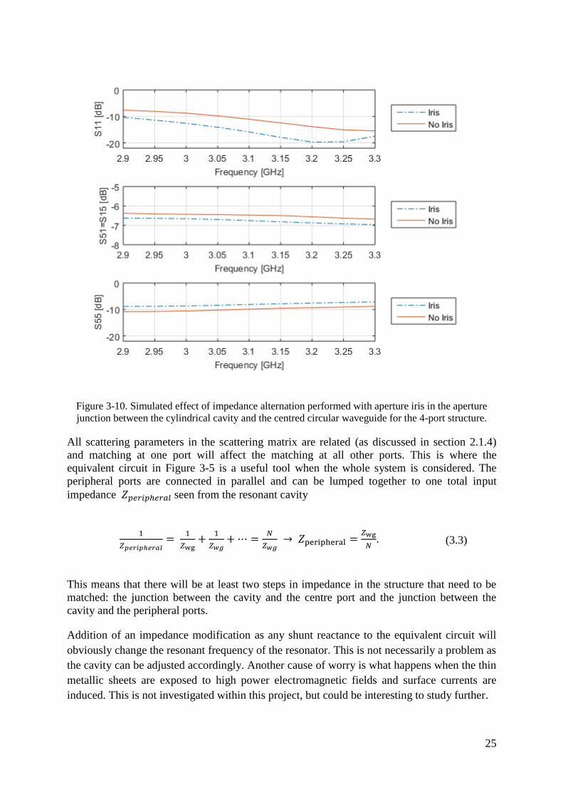
Figure 3-10. Simulated effect of impedance alternation performed with aperture iris in the
aperture junction between the cylindrical cavity and the centred circular waveguide for the 4-
port structure. ........................................................................................................................... 25
Figure 3-11. Simulated leakage shows the isolation between input ports for all modes excited
by TE10 modes in the peripheral waveguides. The mean leakage between ports is marked with
a thick dark-blue line and is at 3.1 GHz: -9.746 dB for the 4-port, -11.213 dB at the 6-port and
-9.547 dB for the 8-port structure. ............................................................................................ 26
Figure 3-12. The cylindrical cavity model in HFSS, with the field function for the Ez field of
the TM020 mode drawn on top of it. ......................................................................................... 28
Figure 3-13. Left: Sketch of the SMA-connector according to data from the datasheet [31].
Right: Model of the SMA-connector made in HFSS. ............................................................. 29
Figure 3-14. Cross-section of the resonant cavity with the Ez-field component of the TM020
shown. The probe is inserted in the region of a maximum of the field to optimize power
transfer. ..................................................................................................................................... 30
Figure 3-15. Modified coaxial pin with added copper cylinder with three variable dimensions
that affect impedance: the cylinder height, cylinder radius and cylinder position. .................. 31
Figure 3-16. Simulated results of variation of the radius of copper cylinders used for
modification of connector probes. ............................................................................................ 32
Figure 3-17. Simulated results of variation of the position of copper cylinders used for
modification of connector probes. ............................................................................................ 32
Figure 3-18. Simulated results of variation of the height of copper cylinders used for
modification of connector probes. ............................................................................................ 33
Figure 3-19. Optimized design of the cylindrical cavity divider and combiner. ..................... 33
Figure 3-20. E-field in the optimized structure when the centre port is excited with 1 W. ..... 34
Figure 3-21. Scattering parameters of the optimized design of the structure........................... 34
Figure 3-22. The final design from above. ............................................................................... 35
Figure 3-23. Cross-section of the final design. ........................................................................ 36
Figure 3-24. The fabricated structures with the peripheral ports on the lid (orange) of the box
to the left and the centre port at the bottom of the box (red) to the right. The SMA connectors
(yellow) and screws that close the box (grey) are also seen. ................................................... 36
Figure 3-25. Surface currents plotted on the cylindrical cavity. The upper corner is of special
interest as it is the place for the junction in the fabricated prototype. ...................................... 37
Figure 3-26. The cylindrical cavity box and the lid, both in aluminium, surrounding the cavity
that the divider and combiner are based on. ............................................................................. 37

xv
Figure 3-27. Measurements and tolerances of the copper cylinders used for probe
modification. The left cylinder is the centre port modification to the connectors at port 1-8 and
the right cylinder is the peripheral port modification to the connector at port 9. ..................... 38
Figure 4-1. Measured scattering parameters of Structure 1. The reflection coefficient Sii at the
peripheral ports is less than -16.7 dB for all ports while the reflection coefficient at the centre
port S99 is less than -16.3 dB for 2.9 GHz-3.3 GHz. The coupling parameters S21 andS12 varies
between -9.4 dB and -8.4 dB. ................................................................................................... 40
Figure 4-2. Measured scattering parameters of Structure 2. The reflection coefficient Sii at the
peripheral ports is less than -17.3 dB for all ports while the reflection coefficient at the centre
port S99 is less than -14.8 dB for 2.9 GHz-3.3 GHz. The coupling parameters S21 andS12 varies
between -9.4 dB and -9.24 dB. ................................................................................................. 41
Figure 4-3. Simulated scattering parameters from the design process. The reflection
coefficient Sii at the peripheral ports is less than -19.1 dB for all ports while the reflection
coefficient at the centre port S99 is less than -17.7 dB for 2.9 GHz-3.3 GHz. The coupling
parameters S21 andS12 varies between -9.13 and -9.04 dB. ...................................................... 41
Figure 4-4. Average peripheral port return loss and insertion loss for the structures. The
measured return loss of the structures shows a more broadband behaviour than the simulated
values. ....................................................................................................................................... 42
Figure 4-5. Centre port return loss and insertion loss for the structures. The simulated result
show smaller insertion loss than the measurement, while the measured centre port return loss
behaviour is very similar to the simulation. ............................................................................. 43
Figure 4-6. Numbering of the peripheral ports, ports 1-8. The centre port on the opposite side
of the cavity is port number 9. .................................................................................................. 43
Figure 4-7. Measured leakage between peripheral ports for structure 1 and structure 2 and
corresponding values from the simulated model. The best isolation is found between port 1
and 4 and port 1 and 6. ............................................................................................................. 44
Figure 4-8. Histogram over the deviation in combiner power output for eight combined input
signals of Pin=1 dBm with a phase deviation of ±2 degrees, ±5 degrees and ±10 degrees. ..... 45
Figure 4-9. Histogram over the deviation in combiner power output for eight combined input
signals of Pin=1±0.1 dBm, Pin=1±0.5 dBm and Pin=1±1 dBm. ................................................ 46
Figure 4-10. Back-to-back setup, where the peripheral ports of the two structures are
connected through SMA-adapters ............................................................................................ 47
Figure 4-11. Scattering parameters from measurement and simulation of the back-to-back
setup as seen in Figure 4-10. .................................................................................................... 48
Figure 4-12. Return loss and insertion loss for passive divider-combiner combination. Both
structure 1 and structure 2 are tested as divider and combiner respectively. ........................... 49
xvi
Figure 4-13. Broadband measurement of the back-to-back setup between 0.5 GHz and 20
GHz with simulated values as comparison for 2 GHz to 4 GHz. ............................................. 50
Figure 4-14. Schematic view of the active test setup where the peripheral ports of the structure
are connected to solid state power amplifiers. The overall increase in Pout should be equal to
the amplifier gain, G dB. .......................................................................................................... 51
Figure 4-15. The loss in gain as the bias is removed from a number of amplifiers when the
amplifiers are in their linear region. “Port 1” in the legend means that the amplifier at port 1 is
unbiased, “Port 1,5” means that the amplifiers at port 1 and port 5 are unbiased, and so on. . 52
Figure 4-16. The loss in gain as the bias is removed from a number of amplifiers when the
amplifiers are saturated. “Port 1” in the legend means that the amplifier at port 1 is unbiased,
“Port 1,5” means that the amplifiers at port 1 and port 5 are unbiased, and so on. ................. 53
Figure 4-17. The simulated losses in gain as an amplifier taken out of operation. “Port 1” in
the legend means that the amplifier at port 1 is unbiased ,“Port 1,5” means that the amplifiers
at port 1 and port 5 are unbiased, and so on. ............................................................................ 54
Figure 4-18. Network for test of methods for improvement of the graceful degradation. The
box with the question mark was replaced with different type of terminations and components.
.................................................................................................................................................. 55
Figure 4-19. Result of the test of different ways to improve the graceful degradation. The best
result for 2.9 GHz to 3.3 GHz is achieved when the failed amplifier is replaced with a phase
shift of 15°. ............................................................................................................................... 56

xvii

xviii
LIST OF TABLES Table 2-1. Electric and magnetic field expressions for TEnm and TMnm modes in a circular
waveguide. [7] ............................................................................................................................ 4
Table 2-2. Values of 𝑝𝑛𝑚′ and 𝑝𝑛𝑚 for TEnm and TMnm modes respectively, in circular
waveguides. ................................................................................................................................ 5
Table 2-3. Comparison between selected radial cavity-based combiner designs. ................... 15
Table 2-4. Comparison between selected radial non-cavity-based combiner designs. ............ 16
Table 3-1. Final measurements of the optimized design. ......................................................... 35

xix

1
1 INTRODUCTION
Today, military and space industries often demand technology with highest possible
performance in combination with excellent reliability, as well as lowest possible size and
weight. This also applies for radar and satellite communication, where the ambition to
increase the range requires solutions to generate high output power at microwave frequencies.
Robust, compact and high performing amplifier solutions are crucial constituents in radar and
wireless communication systems.
Today, the travelling wave tube amplifier (TWTA) is dominating for RF frequencies since it
is a well-tested and reliable solution, albeit with some drawbacks. TWTAs are expensive,
require a considerable warm-up time and very high DC voltage, while being heavy and space
consuming devices, especially for low-frequencies bands [1, 2].
However, the performance of solid state power amplifiers (SSPA) has improved rapidly over
the decades with affordable and reliable devices as a result. One of the more promising
technologies is the GaN transistor that shows very high break down voltage and high radiation
tolerance [1]. Today, devices with output powers as high as hundreds of Watts are available
[3]. Parallel to this technological development, the interest has grown in finding ways to use
SSPAs for high power generation at microwave frequencies. The power limitation of the
SSPA means that a number of SSPAs are required to generate high output powers. This is
where efficient power combiners become crucial for the introduction of high frequent SSPA
based high power amplifier solutions. Radial N-way combiners are compact, reliable and offer
low-loss combination of power in one single step, which makes them suitable for the radar
application.
The SSPAs in combination with power combining provides additional robustness as the
system can operate even though one or more of the SSPAs stop working, albeit with
decreased efficiency. This is called graceful degradation of power [4] and is a great
advantage compared to the TWTA, for which the system fails completely if the TWTA breaks
down. The SSPA based amplifier solution might also allow hot replacement, which means
that broken amplifiers can be replaced in the radar or communication system during
operation.
1.1 Aim of the project
The aim of this thesis project is to analyse the construction of radial N-way amplifiers and to
design, fabricate and evaluate an N-way radial power divider and combiner structure. The
divider and combiner are tested together with power amplifiers to verify the dividing and
combining principle and to study the graceful degradation.
The thesis project focuses on resonant cavity dividers/combiners, and specifically aims to
answer the following questions:

2
How is an N-way radial power divider/combiner consisting of a resonant cavity
constructed?
How sensitive is the radial power combiner to inconsistencies in amplitude and phase
in the input signals?
What are the filter characteristics for the divider and combiner structure?
How does failure of one amplifier affect
o the matching at the other ports?
o the coupling between input and output port?
o the output power?
How good return and insertion loss can be achieved?
The project is divided into four main parts: an initial literature study, analysis, design and
fabrication of the combiner/divider structure, evaluation of the design and fabrication process
and study of the graceful degradation for the designed combiner/divider.
1.2 Demarcations
The construction analysis and the design work will only cover radial power dividers and
combiners based on a cylindrical resonant cavity, as the fabrication of prototypes of this sort
is considered to be feasible within the limited time and resources of the project.
The power amplifiers used are not designed as part of the thesis project, as this would take too
much time. Instead, existing amplifiers are used to evaluate the divider and combiner under
realistic conditions.

3
2 THEORY
This section gives an overview of the theory behind N-way power combining, and goes
through and compares different types of published designs. A reader skilled in the art is
recommended to skip this sections and jump directly to section 2.2 and 2.3 for a brief
introduction to power combiners and dividers and how they can be realized, since section 2.1
covers basic electromagnetic wave theory and fundamentals in microwave engineering. In the
theory section, the word combiner will often be used to describe both combiner and divider
structures as they in general are reciprocal passive networks that can be used in both
applications.
2.1 Cylindrical Cavity Resonators
The cylindrical cavity is in all essential nothing else but a cylindrical waveguide shorted at
both ends with conducting plates, forming a closed cylinder with conducting walls. This
relation with cylindrical waveguides is also reflected in the electro-magnetic field expressions
and modes, as will be discussed in section 2.1.1.
Resonance is a phenomenon occurring when a wave travels a certain distance and is thereafter
reflected so that the incident and reflected waves interfere constructively. For waves travelling
in the propagation direction in hollow waveguides this distance is 𝑛 ∙ 𝜆 2⁄ , where 𝑛 is any
positive integer. For circular symmetries, electromagnetic fields are related to the Bessel
function, which makes the criteria for resonance somewhat more mathematically complex.
The circular symmetry of a cylindrical cavity leads to only two dimensions where resonance
can occur: the height of the cylinder 𝑑 (propagation direction) and the radius of the cylinder 𝑎
(transverse direction). By careful design of the cylinder, specific resonant frequencies can
resonate in the structure.
Figure 2-1. Schematic picture of a resonant cylindrical cavity with examples of resonant waves shown
in height and radial dimensions.
The perfect, lossless resonator has no openings for excitation or signal output. Hence, waves
with the resonant frequency will in theory resonate forever in the cavity if the surface material
is perfectly conducting. However, as input and output ports are added to the cavity, addition
of resistive and reactive elements disturbs the perfect resonator which may cause a shift of the
resonant frequency and can cause losses. In real life, the walls will also introduce
imperfections as metal is not perfectly conducting.
The parallel resonant circuit model [5] is a useful tool to describe the resonant cavity in an
equivalent circuit, as shown in Figure 2-2. This model is convenient when the resonator
should interact with surrounding networks or components, and can be used in impedance
calculations and to relate the Q-factor to resistive and reactive components of the resonator
[6].
4
Figure 2-2. Lumped parallel resonant circuit.
2.1.1 Electromagnetic Fields in Cylindrical Cavities
The derivation of the field expressions for cylindrical cavities is simplified by the fact that the
cylindrical cavity is a special case of circular waveguides. The shortened ends of the
waveguide, creating the cavity, can simply be considered as two additional boundary
conditions. The field expressions for a circular waveguide are listed in Table 2-1.
Table 2-1. Electric and magnetic field expressions for TEnm and TMnm modes
in a circular waveguide. [7]
Field TE𝑛𝑚 mode TM𝑛𝑚 mode
𝐸𝑧 0 (𝐴 sin𝑛∅ + 𝐵 cos 𝑛∅)𝐽𝑛(𝑘𝑐𝜌)𝑒−𝑗𝛽𝑧
𝐻𝑧 (𝐴 sin𝑛∅ + 𝐵 cos 𝑛∅)𝐽𝑛(𝑘𝑐𝜌)𝑒−𝑗𝛽𝑧 0
𝐸𝜌 −𝑗𝜔𝜇𝑛
𝑘𝑐2𝜌
(𝐴 cos 𝑛∅ − 𝐵 sin𝑛∅)𝐽𝑛(𝑘𝑐𝜌)𝑒−𝑗𝛽𝑧 −𝑗𝛽
𝑘𝑐
(𝐴 sin 𝑛∅ + 𝐵 cos 𝑛∅)𝐽𝑛′ (𝑘𝑐𝜌)𝑒−𝑗𝛽𝑧
𝐸∅ −𝑗𝜔𝜇
𝑘𝑐
(𝐴 sin𝑛∅ + 𝐵 cos𝑛∅)𝐽𝑛′ (𝑘𝑐𝜌)𝑒−𝑗𝛽𝑧
−𝑗𝛽𝑛
𝑘𝑐2𝜌
(𝐴 cos 𝑛∅ − 𝐵 sin𝑛∅)𝐽𝑛(𝑘𝑐𝜌)𝑒−𝑗𝛽𝑧
𝐻𝜌 −𝑗𝛽
𝑘𝑐
(𝐴 sin𝑛∅ + 𝐵 cos 𝑛∅)𝐽𝑛′ (𝑘𝑐𝜌)𝑒−𝑗𝛽𝑧
−𝑗𝜔휀𝑛
𝑘𝑐2𝜌
(𝐴 cos 𝑛∅ − 𝐵 sin 𝑛∅)𝐽𝑛(𝑘𝑐𝜌)𝑒−𝑗𝛽𝑧
𝐻∅ −𝑗𝛽𝑛
𝑘𝑐2𝜌
(𝐴 cos 𝑛∅ − 𝐵 sin 𝑛∅)𝐽𝑛(𝑘𝑐𝜌)𝑒−𝑗𝛽𝑧 −𝑗𝜔휀
𝑘𝑐
(𝐴 sin𝑛∅ + 𝐵 cos 𝑛∅)𝐽𝑛′ (𝑘𝑐𝜌)𝑒−𝑗𝛽𝑧
The fields are divided into transverse electric waves, denoted TE𝑛𝑚, and transverse magnetic
waves, denoted TM𝑛𝑚, where “transverse” means that no field exists in the propagation
direction, 𝑧 . All expressions contain the Bessel function of the first kind, 𝐽𝑛(𝑘𝑐𝜌), or its
derivative, 𝐽𝑛′ (𝑘𝑐𝜌). The Bessel function has 𝑚-1 extreme points, and a plot describing the
behaviour of the Bessel function is displayed in Figure 2-3.

5
Figure 2-3. The behaviour of the Bessel function of first kind.
The circular waveguide field functions satisfy the boundary conditions for the side wall in the
cylindrical resonator when 𝐽𝑛(𝑘𝑐𝜌) = 0 or 𝐽𝑛′ (𝑘𝑐𝜌) = 0. For TE𝑛𝑚 modes, the root is often
called 𝑝𝑛𝑚′ so that 𝐽𝑛(𝑝𝑛𝑚
′ ) = 0, and similarly, the root for TE𝑛𝑚 modes is often called 𝑝𝑛𝑚
so that 𝐽𝑛(𝑝𝑛𝑚) = 0. Some of the values of the roots are listed in Table 2-2 below.
Table 2-2. Values of 𝑝𝑛𝑚′ and 𝑝𝑛𝑚for TEnm and TMnm modes respectively, in circular waveguides.
𝑛 𝑝𝑛1′ 𝑝𝑛2
′ 𝑝𝑛3′ 𝑝𝑛1 𝑝𝑛2 𝑝𝑛3
0 3.832 7.016 10.174 2.405 5.520 8.654
1 1.841 5.331 8.536 3.832 7.016 10.174
2 3.054 6.706 9.970 5.135 8.417 11.620
To accurately describe the field in a cylindrical cavity, the shorted planes at 𝑧 = 0, 𝑑 must be
accounted for. Pozar [7] does this, by writing the expression for the transverse fields as below
�⃑� 𝑡(𝜌, 𝜙, 𝑧) = 𝑒 (𝜌, 𝜙)(𝐴+𝑒−𝑗𝛽𝑛𝑚𝑧 + 𝐴−𝑒+𝑗𝛽𝑛𝑚𝑧) (2.1)
where the two functions 𝑒 (𝜌, 𝜙) and (𝐴+𝑒−𝑗𝛽𝑛𝑚𝑧 + 𝐴−𝑒+𝑗𝛽𝑛𝑚𝑧) represents the transverse
variation of the mode and the amplitudes of the forward and backward wave respectively.
These functions are both affected by the boundary condition set by the shorted planes: �⃑� 𝑡 = 0
for 𝑧 = 0, 𝑑. The solution to (2.1) with these boundary conditions gives that the forward and
backward wave amplitude must be inversely related as 𝐴+ = −𝐴− , which implies that
𝐴+ sin(𝛽𝑛𝑚𝑑) = 0. The latter relates the dimensions of the cavity to the modes that can exist
in it since the solution to the equation is 𝛽𝑛𝑚𝑑 = 𝑙𝜋 where 𝑙 is any integer ≥ 0 [7].
2.1.2 Resonant Modes
As discussed in the previous section, a number of modes with different mode indices 𝑛𝑚 can
propagate in waveguides. For the cylindrical cavity, standing waves can also occur in the
6
propagation direction leading to yet another mode index. Hence, cylindrical cavities can
support fields such as TE𝑛𝑚𝑙 and TM𝑛𝑚𝑙.
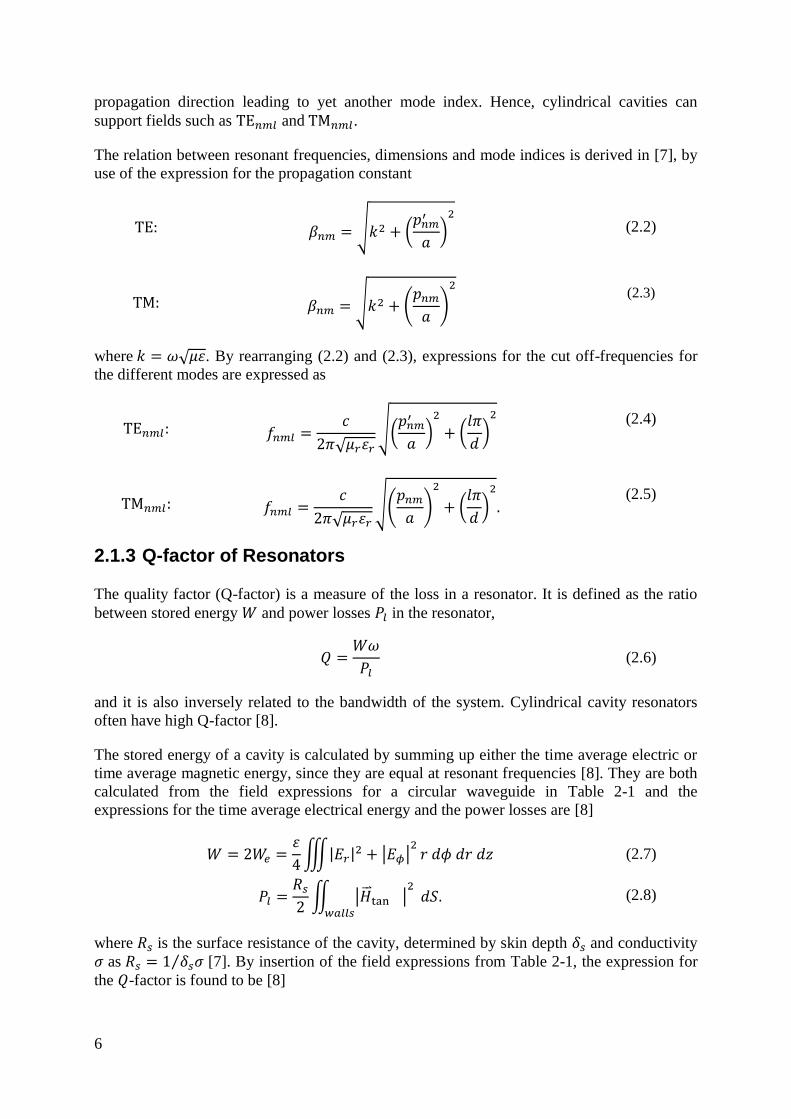
The relation between resonant frequencies, dimensions and mode indices is derived in [7], by
use of the expression for the propagation constant
TE: 𝛽𝑛𝑚 = √𝑘2 + (
𝑝𝑛𝑚′
𝑎)2
(2.2)
TM: 𝛽𝑛𝑚 = √𝑘2 + (𝑝𝑛𝑚
𝑎)
2
(2.3)
where 𝑘 = 𝜔√𝜇휀. By rearranging (2.2) and (2.3), expressions for the cut off-frequencies for
the different modes are expressed as
TE𝑛𝑚𝑙: 𝑓𝑛𝑚𝑙 =
𝑐
2𝜋√𝜇𝑟휀𝑟
√(𝑝𝑛𝑚
′
𝑎)2
+ (𝑙𝜋
𝑑)2
(2.4)
TM𝑛𝑚𝑙: 𝑓𝑛𝑚𝑙 =𝑐
2𝜋√𝜇𝑟휀𝑟
√(𝑝𝑛𝑚
𝑎)
2
+ (𝑙𝜋
𝑑)2
. (2.5)
2.1.3 Q-factor of Resonators
The quality factor (Q-factor) is a measure of the loss in a resonator. It is defined as the ratio
between stored energy 𝑊 and power losses 𝑃𝑙 in the resonator,
𝑄 =
𝑊𝜔
𝑃𝑙 (2.6)
and it is also inversely related to the bandwidth of the system. Cylindrical cavity resonators
often have high Q-factor [8].
The stored energy of a cavity is calculated by summing up either the time average electric or
time average magnetic energy, since they are equal at resonant frequencies [8]. They are both
calculated from the field expressions for a circular waveguide in Table 2-1 and the
expressions for the time average electrical energy and the power losses are [8]
𝑊 = 2𝑊𝑒 =
휀
4∭|𝐸𝑟|
2 + |𝐸𝜙|2𝑟 𝑑𝜙 𝑑𝑟 𝑑𝑧 (2.7)
𝑃𝑙 =
𝑅𝑠
2∬ |�⃑⃑� tan |
2
𝑤𝑎𝑙𝑙𝑠
𝑑𝑆. (2.8)
where 𝑅𝑠 is the surface resistance of the cavity, determined by skin depth 𝛿𝑠 and conductivity
𝜎 as 𝑅𝑠 = 1 𝛿𝑠𝜎⁄ [7]. By insertion of the field expressions from Table 2-1, the expression for
the 𝑄-factor is found to be [8]
7
𝑄 =𝑊𝜔
𝑃𝑙=
𝜆0
𝛿𝑠
[1 − (𝑛
𝑝𝑛𝑚′ )
2
] [(𝑝𝑛𝑚′ )2 + (
𝑙𝜋𝑎ℎ
)2
]
32⁄
2𝜋 [(𝑝𝑛𝑚′ )2 +
2𝑎ℎ
(𝑙𝜋𝑎ℎ
)2
+ (1 −2𝑎ℎ
) (𝑛𝑙𝜋𝑎𝑝𝑛𝑚
′ ℎ)2
]
(2.9)
for the TE-mode. By replacing 𝑝𝑛𝑚′ with 𝑝𝑛𝑚, the 𝑄-factor for the TM-modes is found. As
mentioned earlier, the 𝑄-factor and the bandwidth of the resonator are inversely related to
each other [8]
𝑄 =
1
𝐵𝑊. (2.10)
2.1.4 The Scattering Matrix for Microwave Networks
When working with microwave networks, the tools and models usually applied on low
frequency networks cannot always be applied, and other ways to describe and measure a
circuit must be used. When the wavelength of the high frequency signal is comparable with
the size of the components and the media of transmission, the field expansions in the
component must be considered. This means that the concept of current and voltage are
different in a microwave circuit compared to the low frequency circuit.
The equivalent current and voltage definitions for waveguides are based on the expressions
for electromagnetic waves in section 2.1.1, which means that each mode will have its
individual equivalent current and voltage. A result of the distributed approach is also that
reflections have to be considered for unmatched components, which leads to forward and
backward waves. By writing the transverse field expression [7] as in (2.1), the equivalent
current and voltage can be introduced
�⃑� 𝑡(𝜌, 𝜙, 𝑧) = 𝑒 (𝜌, 𝜙)(𝐴+𝑒−𝑗𝛽𝑛𝑚𝑧 + 𝐴−𝑒+𝑗𝛽𝑛𝑚𝑧)
(2.11) =
𝑒 (𝜌, 𝜙)
𝐶1(𝑉+𝑒−𝑗𝛽𝑛𝑚𝑧 + 𝑉−𝑒+𝑗𝛽𝑛𝑚𝑧)
�⃑⃑� 𝑡(𝜌, 𝜙, 𝑧) = 𝑒 (𝜌, 𝜙)(𝐴+𝑒−𝑗𝛽𝑛𝑚𝑧 + 𝐴−𝑒+𝑗𝛽𝑛𝑚𝑧)
(2.12) =
𝑒 (𝜌, 𝜙)
𝐶2(𝐼+𝑒−𝑗𝛽𝑛𝑚𝑧 − 𝐼−𝑒+𝑗𝛽𝑛𝑚𝑧).
and defined in a more useful manner as
𝑉(𝑧) = 𝑉+𝑒−𝑗𝛽𝑧 + 𝑉−𝑒𝑗𝛽𝑧 (2.13)
𝐼(𝑧) = 𝐼+𝑒−𝑗𝛽𝑧 − 𝐼−𝑒𝑗𝛽𝑧. (2.14)
The definition of 𝑉(𝑧) and 𝐼(𝑧) is chosen so that the characteristic impedance 𝑍0 is defined as
𝑍0 = 𝑉/𝐼.
A common situation to use the equivalent voltage and current is in multiport microwave
networks. For these networks, impedance and admittance may differ between all ports

8
combinations. A convenient way to describe the impedance and admittance of a microwave
system is to create impedance matrices [𝑍] and admittance matrices [𝑌]
[𝑉] = [𝑍][𝐼] ⇒ [
𝑉1
⋮𝑉𝑁
] = [𝑍11 ⋯ 𝑍1𝑁
⋮ ⋱ ⋮𝑍𝑁1 ⋯ 𝑍𝑁𝑁
] [𝐼1⋮𝐼𝑁
] (2.15)
[𝐼] = [𝑌][𝑉] ⇒ [
𝐼1⋮𝐼𝑁
] = [𝑌11 ⋯ 𝑌1𝑁
⋮ ⋱ ⋮𝑌𝑁1 ⋯ 𝑌𝑁𝑁
] [𝑉1
⋮𝑉𝑁
] (2.16)
where each element 𝑍𝑖𝑗 =𝑉𝑖
𝐼𝑗 or 𝑌𝑖𝑗 =
𝐼𝑖
𝑉𝑗 represents the impedance or admittance between
port 𝑖 and 𝑗 [7].
Another matrix model that can be defined from the equivalent voltage and current is the
scattering matrix
[𝑆] = [
𝑆11 ⋯ 𝑆1𝑁
⋮ ⋱ ⋮𝑆𝑁1 ⋯ 𝑆𝑁𝑁
]. (2.17)
The elements of the scattering matrix are known as S-parameters
𝑆𝑖𝑗 =
𝑉𝑖−
𝑉𝑗+ (2.18)
and is a measure of how an incident wave is scattered when travelling from port 𝑗 to 𝑖, or is
incident upon a port 𝑖 [7]. In the latter case, the S-parameter is simply 𝑆𝑖𝑖.
For reciprocal networks
[𝑆] = [𝑆]𝑡 (2.19)
and for lossless networks [8]
∑|𝑆𝑘𝑖|2 = 1
𝑁
𝑘=1
(2.20)
∑ 𝑆𝑘𝑖𝑆𝑘𝑗∗ = 0.
𝑁
𝑘=1
(2.21)
2.1.5 Impedance of Cavity Resonators
In the introduction to this chapter, it was stated that a cavity resonator can be modelled as the
parallel resonant circuit. The calculation of impedance and admittance for such a circuit is a
matter of application of circuit theory

9
𝑌(𝜔) =
1
𝑅+
1
𝑗𝜔𝐿+ 𝑗𝜔𝐶, (2.22)
𝑍 = (𝑌)−1 = (
1
𝑅+
1
𝑗𝜔𝐿+ 𝑗𝜔𝐶)
−1
. (2.23)
The parallel resonant circuit model is related to the real resonant cavity by the relationship
between the 𝑄-factor and the elements of the circuits [5], stating that
𝑄 = 𝜔0𝑅𝐶 (2.24)
where 𝜔0 is the resonant frequency [7]
From these definitions, it is possible to rephrase the impedance for the cylindrical cavity
resonator as [6]
𝑍 = −
𝑗𝜔𝐶
𝜔2 − 𝜔02 (1 +
𝑗𝑄)
. (2.26)
2.1.6 Excitation of Cavities
There are a number of aspects to consider when a resonator should be excited; the coupling
between the resonator and the feed, the frequency of the inserted signal and where the signal
is inserted, to mention a few. In order to excite a certain resonant mode in a cavity, the field
from the excitations should support the field of the resonant mode. This means feeding the
field where it should have a maximum, and by that feeding a resonant field. An example of
this is the excitation of the TM020 mode in a cylindrical cavity resonator in [9].
The electromagnetic wave needs to be be inserted into the cavity in some way to feed the
resonator, which can be done by penetrating the cavity walls with some sort of wave guiding
device. A resonant system can have a number of ports for excitation or signal tapping that will
affect the resonant performance of the cavity, as mentioned in section 2.1. In this section, any
type of usage of ports in the cavity will be called excitation.
A variety of different cavity excitations exist in literature, but the most common means of
excitations are coaxial waveguides, probes, hollow waveguide apertures, and microstrips or
striplines inserted into the cavity. The choice of excitation method can be based upon
properties such as frequency range, power levels or losses, but could also be made
considering practicalities such as volume restrictions or what other microwave networks or
equipment the resonator should be connected to. In this project, waveguide excitation through
apertures and coaxial probes will be discussed.
A useful way to model the effect of the addition of excitation ports is to add their equivalent
circuits to the parallel resonant circuit, and calculate the behaviour of the complete circuit
with circuit theory. For example, the coupling between the excitation feed and the resonator
𝜔0
2 =1
𝐿𝐶. (2.25)

10
can be calculated, which is of interest for maximum power transfer where critically coupled
excitations are desirable [7].
2.2 Power Dividing/Combining
Power dividing and combining is a common need in microwave engineering, and is often
realized through usage of components such as simple T-junctions, Wilkinson dividers or
hybrid couplers [7]. As the components are passive, they can be used as combiners as well as
dividers. A divider or combiner should ideally divide the power perfectly with no insertion or
return losses, or any unwanted leakage between ports on “the same side”. Assuming that a
three-port divider is reciprocal, lossless and has perfectly matched ports, the scattering matrix
will be
[𝑆] = [
0 𝑆12 𝑆13
𝑆12 0 𝑆23
𝑆13 𝑆23 0] (2.27)
where the diagonal elements are zero due to the matched ports. The rules about scattering
parameters for lossless networks (2.20)-(2.21) gives the following equations:
|𝑆12|
2 + |𝑆13|2 = 1, 𝑆23𝑆13
∗ = 0,
|𝑆12|
2 + |𝑆23|2 = 1, 𝑆12𝑆23
∗ = 0, (2.28)
|𝑆13|
2 + |𝑆23|2 = 1, 𝑆13𝑆12
∗ = 0.
However, the three expressions to the right in (2.28) will contradict the expressions to the left
in the same equation. It is not physically possible to have perfect matching at all ports and a
reciprocal and lossless system simultaneously [7].
2.2.1 N-port Power Combining
Power division and power combining play essential part in high power microwave networks,
when amplification is to be achieved with solid state power amplifiers (SSPAs). Traditionally,
SSPAs has not been used in high power amplifications due to their limited output power.
Instead, more powerful amplifiers such as travelling wave tube (TWT) amplifiers have been
used. However, SSPA:s offer great advantages over TWTs due to their small size, short
warm-up time, high efficiency and easy replacement in the case of failure [2].
To increase the power level of SSPAs, power dividers are normally used to split the incoming
signal into N signals that each will be amplified separately by its own designated SSPA. The
N amplified signals are then recombined in a power combiner, resulting in a high power
output. The procedure is illustrated in Figure 2-4.

11
Figure 2-4. Schematic display of power combining/dividing.
Most structures are designed to be passive and reciprocal, and can therefore be used as both
dividers and combiners. For practical reasons, the word combiner will be used for the
structure described in this section of the report, and theory will if nothing else is stated also
apply to dividers.
Power combining of radio frequency signals can be realized with several different techniques
and structures. Different power combining techniques will be discussed further in section
2.2.2 below.
2.2.2 Power Combining Techniques
N-port combination of RF signals can be achieved in many different ways, all of which can be
sorted based on a fundamental property: if they are one-step or multiple-step structures.
Russel [4] provides an overview in different combining techniques, albeit somewhat dated as
new technological advantages have been made since the publication of the article.
The multiple step combiners are typically based on a network of 3-port combiners, arranged
in a binary corporate structure, also known as tree structure [4] as seen in Figure 2-5. This
structure is often seen in microstrip applications. The 3-port combiners can have isolated ports
that prevent leakage which means that this structure can be very efficient in theory, when
different 3-port combiners are assumed to be perfectly matched and lossless. In reality,
however, losses will always occur and will be added in each step, limiting the efficiency of
the structure to a maximum number of steps before the efficiency becomes too low [4].
…
1
2
N-1
N
12
Figure 2-5. Schematic display of binary tree structure with 3 steps and 23 = 8 solid state power
amplifiers.
The multiple step combiners can also be arranged as serial combiners, also known as chain
combiners. Chain structures consist of any number of combiners connected in serial, matched
to the structure with coupling coefficients specific for the position of the combiner [4]. One of
the benefits with the structure is the fact that additional combiners can be added to the
structure as long as it fulfils the coupling coefficient requirements. Drawbacks are high losses
and difficulties to realize the coupling coefficients for a high number of combiners [4].
N-way combining structures differ from the previous two families since they apply 1-step
combination. These are all structures where the input ports are connected in parallel to a
combining node. By this principle, the matching losses decrease significantly compared to the
tree structure combiners. Other advantages of the N-way combiners are graceful degradation
of output power in the case of amplifier failure and the possibility of hot replacements,
meaning that malfunctioning parts of the systems can be replaced during operation. N-way
combiners can be radial as well as non-radial, where the radial N-way combiner is dominating
due to its clever usage of space which allows for a higher number of ports to be combined
[10]. Section 2.3 presents the different methods for realizations of radial N-way combiners as
well as some examples from literature.
The thesis project will cover the construction an N-way combining structure based on a
resonant cavity.
2.3 Methods of Realization of Radial N-way Combiners
The N-way combiners can be divided into three sub-groups: cavity-based combiners, non-
cavity-based combiners and spatial combiners. N-way combiners can sometimes benefit from
a mix between different technologies, and it is not always trivial to sort them into the structure
in Figure 2-6. The choice between different types of N-way combiners is made depending on
requirements such as wanted bandwidth, efficiency, size, isolation, tolerance of amplitude and
phase errors and graceful degradation [10]. The input and output ports of a divider and
combiner should also be compatible with the system where the amplifier solution should be
used and the occurring power levels. For very high output power, e.g. in radar applications
that requires several kW, a waveguide output from the combiner might be the only feasible
solution, which in turn might affect the choice of divider and combiners structure.

13
Figure 2-6. Different N-port power combining techniques arranged in a tree structure.
Even though N-way combiners has been seen in articles since at least the 70’s [11, 9, 12, 13]
it must be considered a relatively young technology that has not been developed enough to
challenge the well-established corporate structures in industrial scale. However, since 2000,
new designs based on radial transmission lines and spatial technology are beginning to show
impressing performance [14, 15].
A brief presentation of the different technologies used for combiners and dividers are listed
below with some interesting examples and a comparison between published designs.
2.3.1 Radial Cavity-Based Combiners
Cavity based radial power combiners guide the electromagnetic wave through the medium
with lowest loss of all: free space. There are two common types of radial cavity combiners
[10]: combiners based on resonant cylindrical cavities and combiners based on substrate
integrated waveguides (SIW), where the latter are a result of implementation of the relatively
new SIW technology [16] and therefore not very widespread.
The ground principle of the cavity combiners is very simple: a circularly symmetric field with
a maximum in the centre point is excited in the cavity by carefully positioned excitation ports,
and the combined signal from the many input ports is tapped out in the centre port. A
cylindrical cavity can be excited with almost any type of waveguide: hollow waveguides,
microstrip patches, coaxial cables, probes etc. To improve bandwidth and matching,
additional sub-cavities or probe designs can be added to the construction, which is done in
[12]. Another factor that affects the efficiency of the combiner is the leakage between input
ports that occurs due to spurious modes in the cavity. In principle, it can be prevented by slits
or barriers that suppress the unwanted modes. However, in most designs no precautions to
improve input isolation are taken. An interesting example of a cylindrical cavity-based
combiner is [17], where a complete combiner SSPA amplifier-system is presented. The
amplifier circuits are mounted as trays at the periphery of the divider and combiner, which
N-port combiner
Multiple step combiners
Corporate Structure
Chain Structure
N-way combiners (one step)
Cavity Combiners
Resonant Cavity SIW
Non-Cavity Combiners
Conical Transmission
line
Radial Transmission
line
Spatial Combiners

14
allows separate testing of each individual port and gives an idea of what a hot replacement-
solution could look like.
The radial cavity-based combiners are well-suited for narrowband solutions as the cavity or
waveguide is designed for a certain resonant frequency. On the plus side, they offer relatively
compact solutions with low intermediate losses. A comparison between typical cavity-based
combiners is listed in Table 2-3. Constructions with more than 16 ports are seldom found in
literature for this technology. Whether the reason for this is that the technology does not
perform well for a high number of ports or not is unknown.
15
Table 2-3. Comparison between selected radial cavity-based combiner designs.
Author Matsumur
a et al
(1987) [9]
Matsumura
et al (1988)
[18]
Tokumitsu
et al (1984)
[12]
Ravindra et
al (2015)
[19]
Shan et al
(2009)
[20]
Li et al
(2014) [21]
Song et al
(2008)
[22]
Song et
al
(2008)
[14]
Denoual et
al (2008)
[17]
He et al
(2016) [23]
Gharekand
(2014) [24]
Technology
Cylindric
al cavity
with slits
Cylindrical
cavity with
slits and sub-
cavity
Cylindrical
cavity with
sub-cavity
Cylindrical
cavity
Cylindrical
cavity
Octagonal
Cavity
Cylindric
al
waveguid
e
SIW Coaxial
cavity
Cylindrical
Cavity
Cylindrical
Cavity
Combined
ports 8 4 8 6 8 8 8 8 16 8 16
Port
Interf
ace
In Coaxial Rectangular
waveguide Coaxial Microstrip Microstrip
Rectangular
waveguide Coaxial Probe Waveguide Probe Coaxial
Out Coaxial Rectangular
waveguide Coaxial
Rectangular
waveguide Coaxial Coaxial Probe Probe Coaxial Probe Waveguide
𝑓0 12 GHz 14 GHz 6 GHz 9.65 GHz 14 GHz 10 GHz 8 GHz 5.25
GHz 18 GHz 29.5 GHz 4.7 GHz
Insertion
Loss (𝑓0) 0.45 dB 0.25 dB 0.2 dB 0.3 dB 0.1 dB 1.8 dB 1 dB 0.2 dB 2 dB -- 0.7 dB
Return
Loss (𝑓0) -- -- 18 dB 20 dB 20 dB 15 dB 15 dB 30 dB 12 dB 15 dB 22 dB
BW
RL>10
dB: 1.13
GHz
IL<0.1 dB:
500 MHz
IL<0.2 dB:
600 MHz
IL<0.3 dB:
200 MHz
RL>20 dB:
1.9 GHz
RL>15 dB:
4 GHz
RL>15
dB:
7 GHz
RL>15
dB:
500
MHz
RL>12 dB:
4.5 GHz
RL>15 dB:
7 GHz
IL<0.7 dB:
600 MHz

16
2.3.2 Radial Non-Cavity-Based Combiners
Non-cavity-based radial combiners are often made of microstrip or stripline, which is
convenient due to their compatibility with integrated circuits, for example MMIC, that allows
dense combiner solutions. To not have to match different technologies in at least one port
might save losses. An advantage with the microstrip technology is that matching and isolation
can be managed with lumped, off-the-shelf components as in [25], which makes this
technology suitable for solutions with high isolation requirements. The large radial
transmission line that is used to combine the input signals limits the bandwidth of the
combiner [10], which together with previous listed characteristics makes this combiner type
suitable for narrow bandwidth combiner in microstrip systems. One feature that makes the
microstrip and stripline combiners attractive are the many design methods available, for
example the ones presented in [25] and [15].
Another type of non-cavity-based radial combiners is the conical transmission line combiners,
as presented in [26]. They transform a coaxial port to a funnel-shaped cavity, with a tapering
design to match the coaxial input ports to the single combination port.
Table 2-4. Comparison between selected radial non-cavity-based combiner designs.
Author Belehoubek et
al (1986) [13]
Fathy et al
(2006) [25]
Jain et al (2014)
[15]
Dirk (2008)
[26]
Technology
Radial
transmission
line
Radial
transmission
line
Radial
transmission
line + coaxial
Conical
Transmission
Line
Combined ports 30 30 16 10
Port
Interface
In Coaxial Coaxial Coaxial Coaxial
Out Coaxial Microstrip/
Coaxial Coaxial
Tapered
Coaxial
𝑓0 11 GHz 12.5 GHz 505.8 MHz 10
Insertion Loss (𝑓0) 0.4 dB 0.55 dB 0.1 dB 0.28 dB
Return Loss (𝑓0) -- 16 dB 22 dB 18.5 dB
BW IL < 0.5 dB:
600 MHz --
RL>15 dB:
40 MHz
RL > 18.5 dB:
4.7 GHz
2.3.3 Spatial Combiners
A technology developed over the last two decades is the spatial power combiner [27], which
usually is presented as complete amplification systems with divider, amplifier and combiner
in one complete network. As the spatial combiners guide the signals through air, and use
antenna interfaces, the intermediate losses are very low. However, antenna coupling factors
may introduce losses. The spatial combiners provide a large bandwidth, and is often used for
high frequencies, making them suitable for applications within communication, where high

17
data transfer is of importance [28]. H. Javadi-Bakhsh and R. Faraji-Dana published a spatial
combiner with 20 elements [27] with tray amplifiers in 2014 with fin-line antenna elements
that show the typical principle behind spatial combiners.

18
3 DIVIDER AND COMBINER DESIGN AND FABRICATION
In this thesis project, a full setup of an SSPA amplifier solution is designed and fabricated,
and then evaluated. This section of the report will cover a conceptual study of cylindrical
cavity combiners and dividers, design of the divider and combiner prototype and fabrication
of the test setup.
3.1 Conceptual Study of Cylindrical Cavity Dividers and Combiners
A simple, conceptual design of a cavity combiner with a circular centre port and rectangular
peripheral ports was developed with inspiration from [9] and [18]. The structure was used to
study the impact of different design parameters.
3.1.1 Cylindrical Cavity
The combiner structure is based on a cylindrical resonant cavity where a chosen mode TM0𝑚0
is excited. The mode index 𝑚 should be two or higher since 𝑚=1 does not have any extreme
point in the 𝐸𝑧-field, and should be chosen in relation to the number of peripheral ports and
the bandwidth of the combiner or designer [9]. In this thesis project, structures based on the
TM020 modes are studied. Equation (2.4) is used to determine the wanted radius of the cavity
in order for to it to support a resonant frequency 𝑓𝑟 for the mode in question.
In order for the cavity height related mode index 𝑙 to be zero, a limitation is set for the cavity
height 𝑑 to never be 𝜆/2 or higher. This should apply to the highest frequency in the wanted
frequency band, with a margin of at least 10 %. With this rule of thumb applied to the
frequency interval of 2.9 GHz-3.3 GHz, the height of the resonant cavity should be 𝑑 < 40.9
mm.
Figure 3-1 shows a mode chart where the TE𝑛𝑚0 and TM𝑛𝑚0 modes from the listed values of
𝑛𝑚 from Table 2-2 are plotted. This can be used to determine if any other – unwanted –
modes might resonate as a result of the excitation of the wanted mode. Unwanted modes are
called spurious modes and there are a number of ways to suppress them. These will not be
discussed within this thesis projects, but the interested reader finds an example of how mode
suppression can be done in a resonant cavity combiner in [9].
19
Figure 3-1. Resonant modes in the cylindrical cavity calculated from the solutions to the Bessel
function from Table 2-2. Some of the modes overlap. The resonant modes closest to TM020 are TM210
and TE120.
From (2.4), it is clear that the resonant frequency should not be affected by variation of cavity
height 𝑑 when 𝑙 = 0. However, another important property of the resonant cavity will vary
with cavity height: the input impedance. Montgomery, Dicke and Purcell [5] describe the
input impedance of a cavity by an example containing a shorted waveguide excited with a
waveguide iris aperture. Exclusion of the impedance contribution from the iris gives the input
impedance for the resonator
𝑍𝑖𝑛 = 𝑍0 tanh([𝛼 + 𝑗𝛽]𝑙) (3.1)
where the attenuation coefficient 𝛼 and the propagation constant 𝛽 are fixed values for a
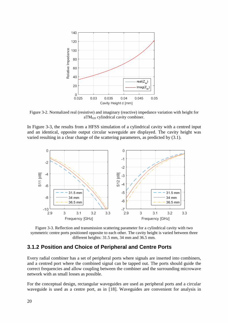
certain mode, leaving the cavity height 𝑙 as only variable. Figure 3-2 below shows how the
normalized input impedance is affected by the cavity height, with the resistive and reactive
components plotted as separate graphs. The resistive part is close to unchanged while the
reactive component varies as the tanh-function, which implies that the cavity height can be
used as a tuning parameter for impedance matching. The detailed calculation of (3.1) is found
in APPENDIX A
20
Figure 3-2. Normalized real (resistive) and imaginary (reactive) impedance variation with height for
aTM020 cylindrical cavity combiner.
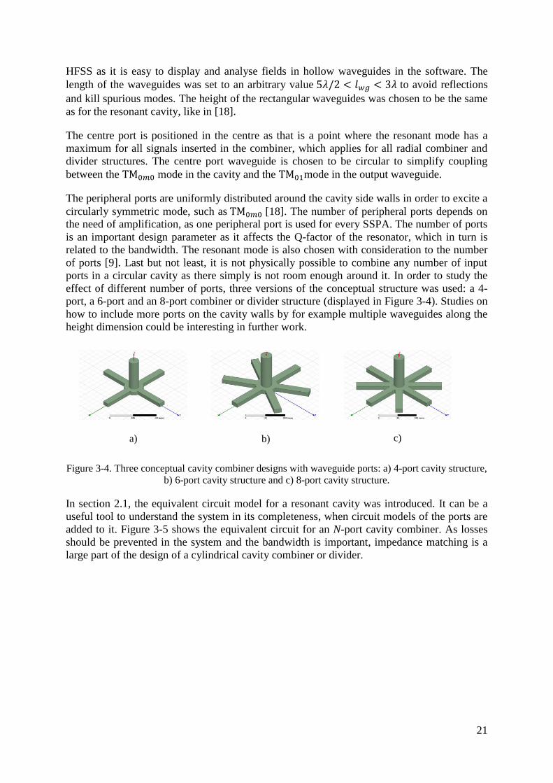
In Figure 3-3, the results from a HFSS simulation of a cylindrical cavity with a centred input
and an identical, opposite output circular waveguide are displayed. The cavity height was
varied resulting in a clear change of the scattering parameters, as predicted by (3.1).
Figure 3-3. Reflection and transmission scattering parameter for a cylindrical cavity with two
symmetric centre ports positioned opposite to each other. The cavity height is varied between three
different heights: 31.5 mm, 34 mm and 36.5 mm.
3.1.2 Position and Choice of Peripheral and Centre Ports
Every radial combiner has a set of peripheral ports where signals are inserted into combiners,
and a centred port where the combined signal can be tapped out. The ports should guide the
correct frequencies and allow coupling between the combiner and the surrounding microwave
network with as small losses as possible.
For the conceptual design, rectangular waveguides are used as peripheral ports and a circular
waveguide is used as a centre port, as in [18]. Waveguides are convenient for analysis in
21
HFSS as it is easy to display and analyse fields in hollow waveguides in the software. The
length of the waveguides was set to an arbitrary value 5𝜆/2 < 𝑙𝑤𝑔 < 3𝜆 to avoid reflections
and kill spurious modes. The height of the rectangular waveguides was chosen to be the same
as for the resonant cavity, like in [18].
The centre port is positioned in the centre as that is a point where the resonant mode has a
maximum for all signals inserted in the combiner, which applies for all radial combiner and
divider structures. The centre port waveguide is chosen to be circular to simplify coupling
between the TM0𝑚0 mode in the cavity and the TM01mode in the output waveguide.
The peripheral ports are uniformly distributed around the cavity side walls in order to excite a
circularly symmetric mode, such as TM0𝑚0 [18]. The number of peripheral ports depends on
the need of amplification, as one peripheral port is used for every SSPA. The number of ports
is an important design parameter as it affects the Q-factor of the resonator, which in turn is
related to the bandwidth. The resonant mode is also chosen with consideration to the number
of ports [9]. Last but not least, it is not physically possible to combine any number of input
ports in a circular cavity as there simply is not room enough around it. In order to study the
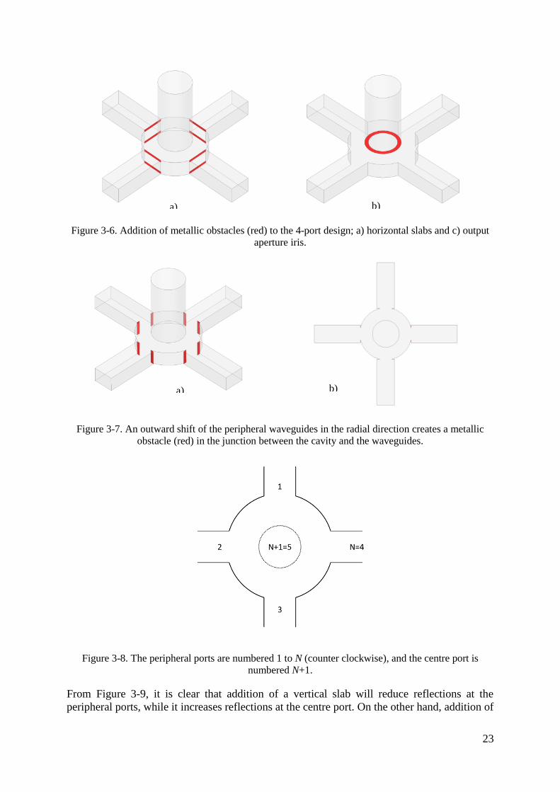
effect of different number of ports, three versions of the conceptual structure was used: a 4-
port, a 6-port and an 8-port combiner or divider structure (displayed in Figure 3-4). Studies on
how to include more ports on the cavity walls by for example multiple waveguides along the
height dimension could be interesting in further work.
Figure 3-4. Three conceptual cavity combiner designs with waveguide ports: a) 4-port cavity structure,
b) 6-port cavity structure and c) 8-port cavity structure.
In section 2.1, the equivalent circuit model for a resonant cavity was introduced. It can be a
useful tool to understand the system in its completeness, when circuit models of the ports are
added to it. Figure 3-5 shows the equivalent circuit for an N-port cavity combiner. As losses
should be prevented in the system and the bandwidth is important, impedance matching is a
large part of the design of a cylindrical cavity combiner or divider.
a) b) c)

22
Figure 3-5. Equivalent circuit of an N-port combiner structure.
3.1.3 Impedance Matching
For waveguide junctions, mechanical modifications of the waveguides can be used to adjust
impedance, and by that reduce reflection losses. Montgomery, Dicke and Purcell [5] describe
how thin metal sheets can be inserted in waveguides to introduce a shunt reactive element 𝑗𝐵,
when the thin metal sheets form a slit through which the electromagnetic field can propagate.
The detailed expressions for this are listed in APPENDIX C. The orientation of the slit
opening determines if the reactive element is inductive or capacitive; a slit parallel with the
electrical field will give rise to a shunt inductance, while a slit perpendicular to the electrical
field will give rise to capacitive impedance [5]. For circular waveguides, no data is found for
the TM0m modes. It is, however, stated that for circular waveguides supporting TE11 modes,
that addition of a metal sheet creating an iris opening gives rise to a shunt inductive
susceptance [5].
Three different modifications of the waveguides in the 4-port structure was tested and
analysed: addition of 7 mm high horizontal slabs to the peripheral waveguides, addition of an
aperture iris rim of 9 mm at the circular, centred waveguide and finally, the radial position of
the peripheral waveguides was shifted outwards so that the walls of the rectangular
waveguides acted as 6.75 mm vertical slabs (as done in [18]). The modifications are shown in
Figure 3-6 and Figure 3-7 below. Figure 3-9 and Figure 3-10 show simulated results of
addition of metallic obstacles in the waveguide aperture junctions. The ports in the designs are
numbered as in Figure 3-8.
23
Figure 3-6. Addition of metallic obstacles (red) to the 4-port design; a) horizontal slabs and c) output
aperture iris.
Figure 3-7. An outward shift of the peripheral waveguides in the radial direction creates a metallic
obstacle (red) in the junction between the cavity and the waveguides.
Figure 3-8. The peripheral ports are numbered 1 to N (counter clockwise), and the centre port is
numbered N+1.
From Figure 3-9, it is clear that addition of a vertical slab will reduce reflections at the
peripheral ports, while it increases reflections at the centre port. On the other hand, addition of
a) b)
a) b)
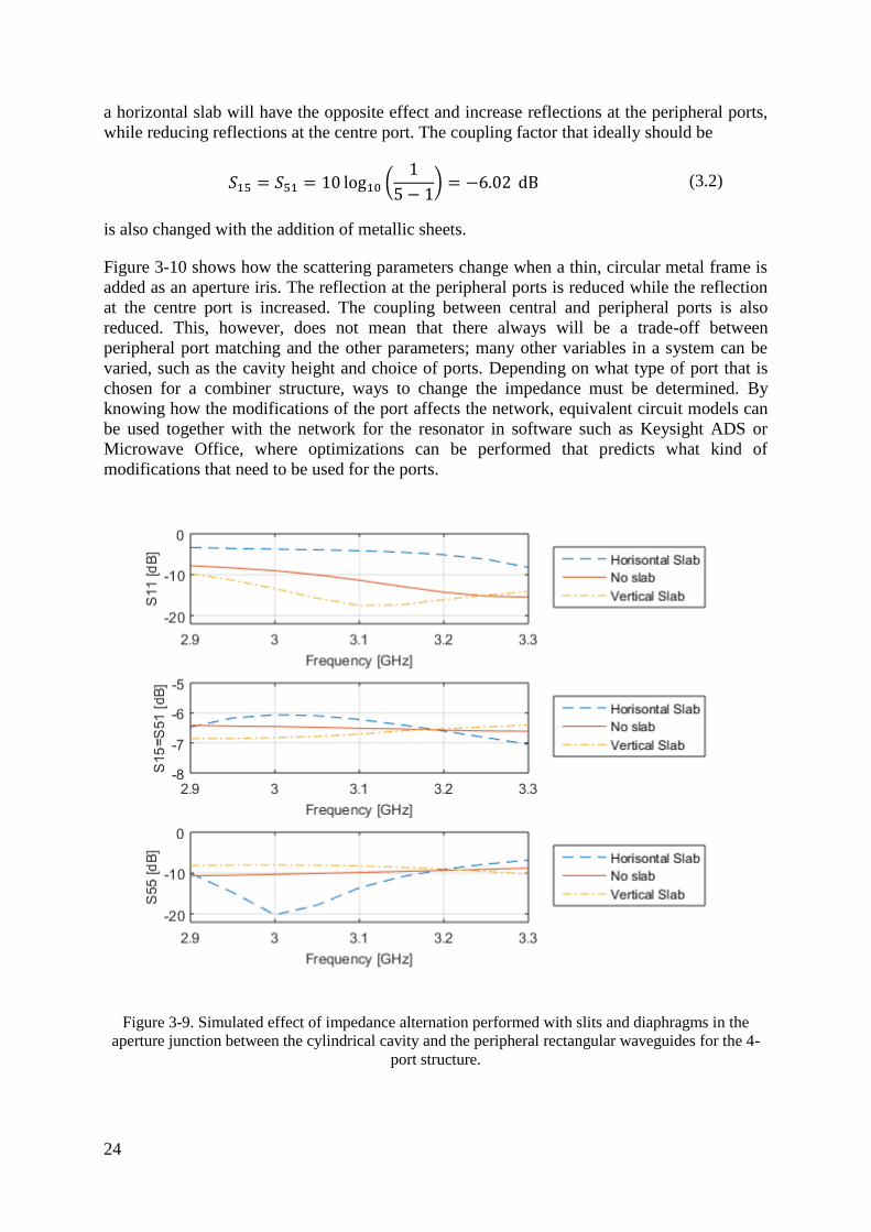
24
a horizontal slab will have the opposite effect and increase reflections at the peripheral ports,
while reducing reflections at the centre port. The coupling factor that ideally should be
𝑆15 = 𝑆51 = 10 log10 (
1
5 − 1) = −6.02 dB (3.2)
is also changed with the addition of metallic sheets.
Figure 3-10 shows how the scattering parameters change when a thin, circular metal frame is
added as an aperture iris. The reflection at the peripheral ports is reduced while the reflection
at the centre port is increased. The coupling between central and peripheral ports is also
reduced. This, however, does not mean that there always will be a trade-off between
peripheral port matching and the other parameters; many other variables in a system can be
varied, such as the cavity height and choice of ports. Depending on what type of port that is
chosen for a combiner structure, ways to change the impedance must be determined. By
knowing how the modifications of the port affects the network, equivalent circuit models can
be used together with the network for the resonator in software such as Keysight ADS or
Microwave Office, where optimizations can be performed that predicts what kind of
modifications that need to be used for the ports.
Figure 3-9. Simulated effect of impedance alternation performed with slits and diaphragms in the
aperture junction between the cylindrical cavity and the peripheral rectangular waveguides for the 4-
port structure.
25
Figure 3-10. Simulated effect of impedance alternation performed with aperture iris in the aperture
junction between the cylindrical cavity and the centred circular waveguide for the 4-port structure.
All scattering parameters in the scattering matrix are related (as discussed in section 2.1.4)
and matching at one port will affect the matching at all other ports. This is where the
equivalent circuit in Figure 3-5 is a useful tool when the whole system is considered. The
peripheral ports are connected in parallel and can be lumped together to one total input
impedance 𝑍𝑝𝑒𝑟𝑖𝑝ℎ𝑒𝑟𝑎𝑙 seen from the resonant cavity
1
𝑍𝑝𝑒𝑟𝑖𝑝ℎ𝑒𝑟𝑎𝑙=
1
𝑍wg+
1
𝑍𝑤𝑔+ ⋯ =
𝑁
𝑍𝑤𝑔 → 𝑍peripheral =
𝑍wg
𝑁. (3.3)
This means that there will be at least two steps in impedance in the structure that need to be
matched: the junction between the cavity and the centre port and the junction between the
cavity and the peripheral ports.
Addition of an impedance modification as any shunt reactance to the equivalent circuit will
obviously change the resonant frequency of the resonator. This is not necessarily a problem as
the cavity can be adjusted accordingly. Another cause of worry is what happens when the thin
metallic sheets are exposed to high power electromagnetic fields and surface currents are
induced. This is not investigated within this project, but could be interesting to study further.
26
3.1.4 Bandwidth
The narrow bandwidth of cylindrical cavity resonators has already been discussed in previous
chapters as well as the fact that addition of ports decreases the Q-factor, hence broaden the
bandwidth [9]. In order to make an accurate comparison between the bandwidth of the three
different concept structures (the 4-port, the 6-port and the 8-port), all three structures should
first be optimized individually as the load from the peripheral ports will vary seen from the
resonator. This was however not done in the scope of this master thesis project.
The bandwidth can be estimated with a mathematical approach, by using the equivalent
circuit model and study the coupling between the ports and the resonators. The bandwidth is
found by calculation of the loaded Q-factor, 𝑄𝑒, that is related to the coupling factor and the
unloaded Q-factor of the resonator.
3.1.5 Isolation
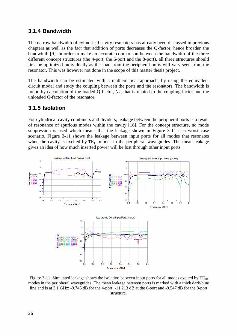
For cylindrical cavity combiners and dividers, leakage between the peripheral ports is a result
of resonance of spurious modes within the cavity [18]. For the concept structure, no mode
suppression is used which means that the leakage shown in Figure 3-11 is a worst case
scenario. Figure 3-11 shows the leakage between input ports for all modes that resonates
when the cavity is excited by TE10 modes in the peripheral waveguides. The mean leakage
gives an idea of how much inserted power will be lost through other input ports.
Figure 3-11. Simulated leakage shows the isolation between input ports for all modes excited by TE10
modes in the peripheral waveguides. The mean leakage between ports is marked with a thick dark-blue
line and is at 3.1 GHz: -9.746 dB for the 4-port, -11.213 dB at the 6-port and -9.547 dB for the 8-port
structure.
27
For better isolation, spurious modes should be identified and suppressed as far as possible. It
is however worth to remember that perfect isolation and perfect port matching and coupling
cannot be achieved simultaneously.
3.2 Design Requirements for Prototype Divider and Combiner
One of the aims of this project was to design and fabricate a prototype divider and combiner
with excellent performance, and to determine its usability in a SSPA based amplifier solution
for radar applications. A literature study was performed where properties of different dividers
and combiners were compared and listed in tables in section 2.3.1-2.3.3. The goal was to
achieve insertion and reflection loss as good as, or better than, similar published designs.
An important factor in the choice of technology was of course the feasibility of the
fabrication, as the project was limited by both time and funds.
3.2.1 Amplifier
The design was initially planned to be used together with an amplifier that operates between
2.9 GHz and 3.3 GHz, and the design is therefore optimized for these frequencies. However,
due to practicalities, the amplifier in the actual test setup was replaced with InGaP HBT
amplifiers that operate at DC-4 GHz with a listed typical gain of 11.7 dB and a P1dB of 17.3
dBm [29]. All eight amplifiers were measured and the variation in gain and phase between the
individual amplifiers were so small that they were considered to be identical.
3.2.2 Central and Peripheral Ports
Radar requires large output powers as the range of the radar is related to the transmit power as
𝑅 ∝ √𝑃𝑡𝑟𝑎𝑛𝑠𝑚𝑖𝑡4
[30]. For military radar, the output power levels are often of the order of
several kW, hence, the combiner and its output must be able to handle such power levels. In a
real life application, it is likely necessary for the combiner to have a waveguide output, as
they are able to handle very high powers safely. The initial design idea was therefore to use a
waveguide output for the prototype combiner as well. That was, however, changed during the
design process due to time limitations and coaxial contacts were used as input and output
ports for both the divider and combiner, which is discussed in section 3.3.2.
3.2.3 Number of Ports
Another consequence of the high output power required is that a high number of amplifiers
must be used, as the performance of SSPAs is still limited to hundreds of Watts. As many
ports as 50-100 might be needed in real life applications. In order to reduce the complexity of
the design, it was decided that the prototype should have eight input ports. This is a major
limitation in this study, as the number of ports is an important aspect to consider in choice of
technology, and also affects the characteristics of the combiner design.
3.2.4 Bandwidth
The bandwidth of the combiner and divider was set to be the same as for the amplifier that
was initially supposed to be used in the test setup: 2.9 GHz-3.3 GHz. This results in a
bandwidth of 13 %.
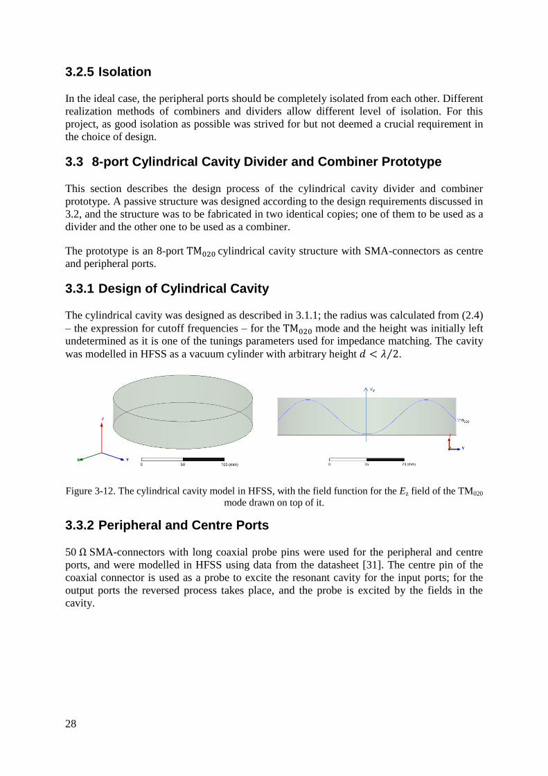
28
3.2.5 Isolation
In the ideal case, the peripheral ports should be completely isolated from each other. Different
realization methods of combiners and dividers allow different level of isolation. For this
project, as good isolation as possible was strived for but not deemed a crucial requirement in
the choice of design.
3.3 8-port Cylindrical Cavity Divider and Combiner Prototype
This section describes the design process of the cylindrical cavity divider and combiner
prototype. A passive structure was designed according to the design requirements discussed in
3.2, and the structure was to be fabricated in two identical copies; one of them to be used as a
divider and the other one to be used as a combiner.
The prototype is an 8-port TM020 cylindrical cavity structure with SMA-connectors as centre
and peripheral ports.
3.3.1 Design of Cylindrical Cavity
The cylindrical cavity was designed as described in 3.1.1; the radius was calculated from (2.4)
– the expression for cutoff frequencies – for the TM020 mode and the height was initially left
undetermined as it is one of the tunings parameters used for impedance matching. The cavity
was modelled in HFSS as a vacuum cylinder with arbitrary height 𝑑 < 𝜆 2⁄ .
Figure 3-12. The cylindrical cavity model in HFSS, with the field function for the Ez field of the TM020
mode drawn on top of it.
3.3.2 Peripheral and Centre Ports
50 Ω SMA-connectors with long coaxial probe pins were used for the peripheral and centre
ports, and were modelled in HFSS using data from the datasheet [31]. The centre pin of the
coaxial connector is used as a probe to excite the resonant cavity for the input ports; for the
output ports the reversed process takes place, and the probe is excited by the fields in the
cavity.

29
Figure 3-13. Left: Sketch of the SMA-connector according to data from the datasheet [31].
Right: Model of the SMA-connector made in HFSS.
To optimize power transfer and excite the correct mode, the peripheral ports should be located
at the radial distance 𝜌 where 𝐸𝑧 has a maximum [9]. The field expression for 𝐸𝑧 is taken
from Table 2-1, and the field maximum can be found from
𝜕
𝜕𝜌(𝐴 sin 𝑛∅ + 𝐵 cos 𝑛∅)𝐽𝑛(𝑘𝑐𝜌)𝑒−𝑗𝛽𝑧 = 0. (3.4)
It is clear from the expression that only the Bessel function is dependent on 𝜌 , and the
equation can be simplified to
𝐽𝑛′ (𝑘𝑐𝜌) = 0 (3.5)
and so, the solution 𝑝𝑛𝑚′ = 𝑘𝑐𝜌 for 𝑛𝑚 = 02 can be found from Table 2-2. The calculated
radial distance 𝜌 = 59.2 mm was used as a starting point for optimizations in HFSS. After
optimizations, the final radial distance was set to 𝜌 = 62.04 mm. Figure 3-14 shows the 𝐸-
field in the cavity when the ports are positioned as described and the centre positioned input
port is excited. Below the resonator, the 𝐸𝑧-field for the TM020 mode is plotted to show the
positions of the theoretical maxima.
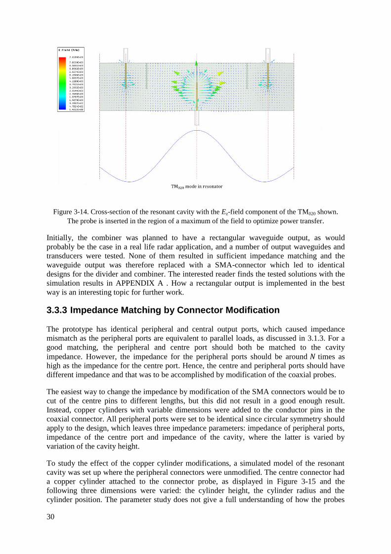
30
Figure 3-14. Cross-section of the resonant cavity with the Ez-field component of the TM020 shown.
The probe is inserted in the region of a maximum of the field to optimize power transfer.
Initially, the combiner was planned to have a rectangular waveguide output, as would
probably be the case in a real life radar application, and a number of output waveguides and
transducers were tested. None of them resulted in sufficient impedance matching and the
waveguide output was therefore replaced with a SMA-connector which led to identical
designs for the divider and combiner. The interested reader finds the tested solutions with the
simulation results in APPENDIX A . How a rectangular output is implemented in the best
way is an interesting topic for further work.
3.3.3 Impedance Matching by Connector Modification
The prototype has identical peripheral and central output ports, which caused impedance
mismatch as the peripheral ports are equivalent to parallel loads, as discussed in 3.1.3. For a
good matching, the peripheral and centre port should both be matched to the cavity
impedance. However, the impedance for the peripheral ports should be around 𝑁 times as
high as the impedance for the centre port. Hence, the centre and peripheral ports should have
different impedance and that was to be accomplished by modification of the coaxial probes.
The easiest way to change the impedance by modification of the SMA connectors would be to
cut of the centre pins to different lengths, but this did not result in a good enough result.
Instead, copper cylinders with variable dimensions were added to the conductor pins in the
coaxial connector. All peripheral ports were set to be identical since circular symmetry should
apply to the design, which leaves three impedance parameters: impedance of peripheral ports,
impedance of the centre port and impedance of the cavity, where the latter is varied by
variation of the cavity height.
To study the effect of the copper cylinder modifications, a simulated model of the resonant
cavity was set up where the peripheral connectors were unmodified. The centre connector had
a copper cylinder attached to the connector probe, as displayed in Figure 3-15 and the
following three dimensions were varied: the cylinder height, the cylinder radius and the
cylinder position. The parameter study does not give a full understanding of how the probes
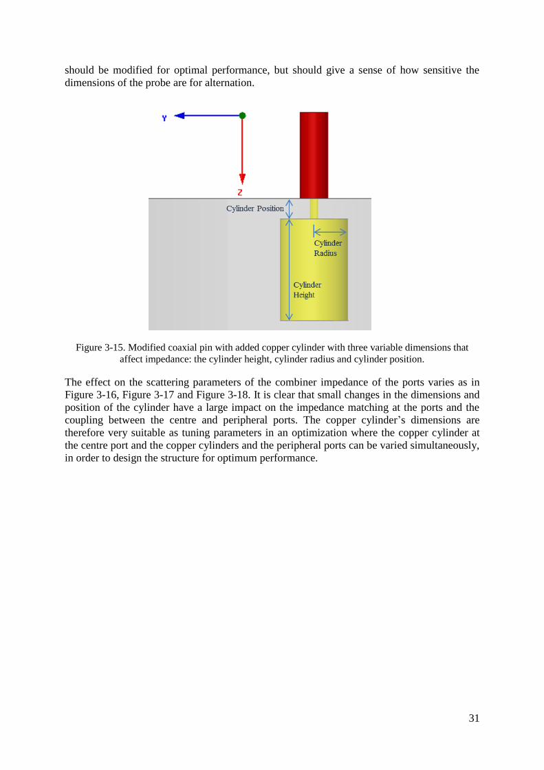
31
should be modified for optimal performance, but should give a sense of how sensitive the
dimensions of the probe are for alternation.
Figure 3-15. Modified coaxial pin with added copper cylinder with three variable dimensions that
affect impedance: the cylinder height, cylinder radius and cylinder position.
The effect on the scattering parameters of the combiner impedance of the ports varies as in
Figure 3-16, Figure 3-17 and Figure 3-18. It is clear that small changes in the dimensions and
position of the cylinder have a large impact on the impedance matching at the ports and the
coupling between the centre and peripheral ports. The copper cylinder’s dimensions are
therefore very suitable as tuning parameters in an optimization where the copper cylinder at
the centre port and the copper cylinders and the peripheral ports can be varied simultaneously,
in order to design the structure for optimum performance.

32
Figure 3-16. Simulated results of variation of the radius of copper cylinders used for modification of
connector probes.
Figure 3-17. Simulated results of variation of the position of copper cylinders used for modification of
connector probes.
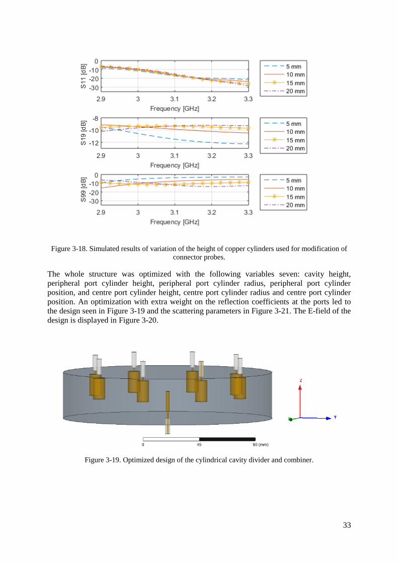
33
Figure 3-18. Simulated results of variation of the height of copper cylinders used for modification of
connector probes.
The whole structure was optimized with the following variables seven: cavity height,
peripheral port cylinder height, peripheral port cylinder radius, peripheral port cylinder
position, and centre port cylinder height, centre port cylinder radius and centre port cylinder
position. An optimization with extra weight on the reflection coefficients at the ports led to
the design seen in Figure 3-19 and the scattering parameters in Figure 3-21. The E-field of the
design is displayed in Figure 3-20.
Figure 3-19. Optimized design of the cylindrical cavity divider and combiner.
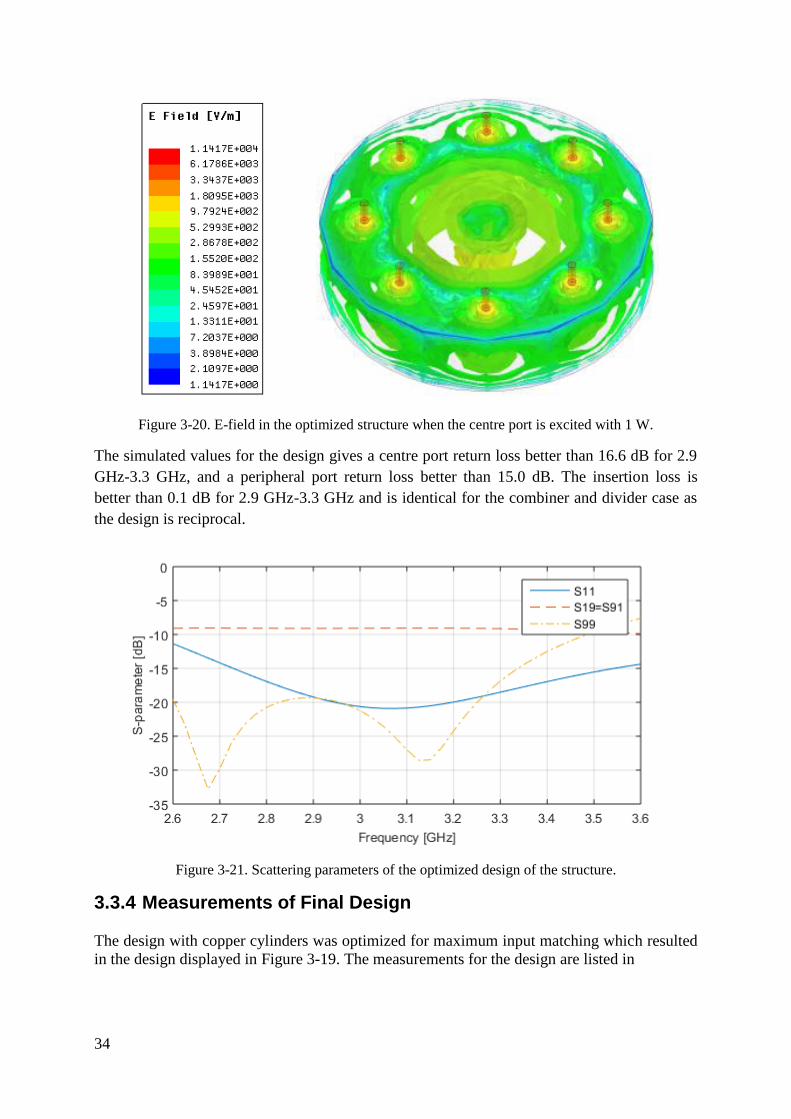
34
Figure 3-20. E-field in the optimized structure when the centre port is excited with 1 W.
The simulated values for the design gives a centre port return loss better than 16.6 dB for 2.9
GHz-3.3 GHz, and a peripheral port return loss better than 15.0 dB. The insertion loss is
better than 0.1 dB for 2.9 GHz-3.3 GHz and is identical for the combiner and divider case as
the design is reciprocal.
Figure 3-21. Scattering parameters of the optimized design of the structure.
3.3.4 Measurements of Final Design
The design with copper cylinders was optimized for maximum input matching which resulted
in the design displayed in Figure 3-19. The measurements for the design are listed in

35
Table 3-1. Final measurements of the optimized design.
Design Parameter Value [mm]
𝑎𝑟𝑒𝑠 85.00
𝑑𝑟𝑒𝑠 37.44
ℎ1 17.02
ℎ2 16.20
𝑟1 5.00
𝑟2 1.50
𝑧1 3.06
𝑧2 5.70
𝜌𝑝𝑜𝑟𝑡 62.04
Figure 3-22. The final design from above.
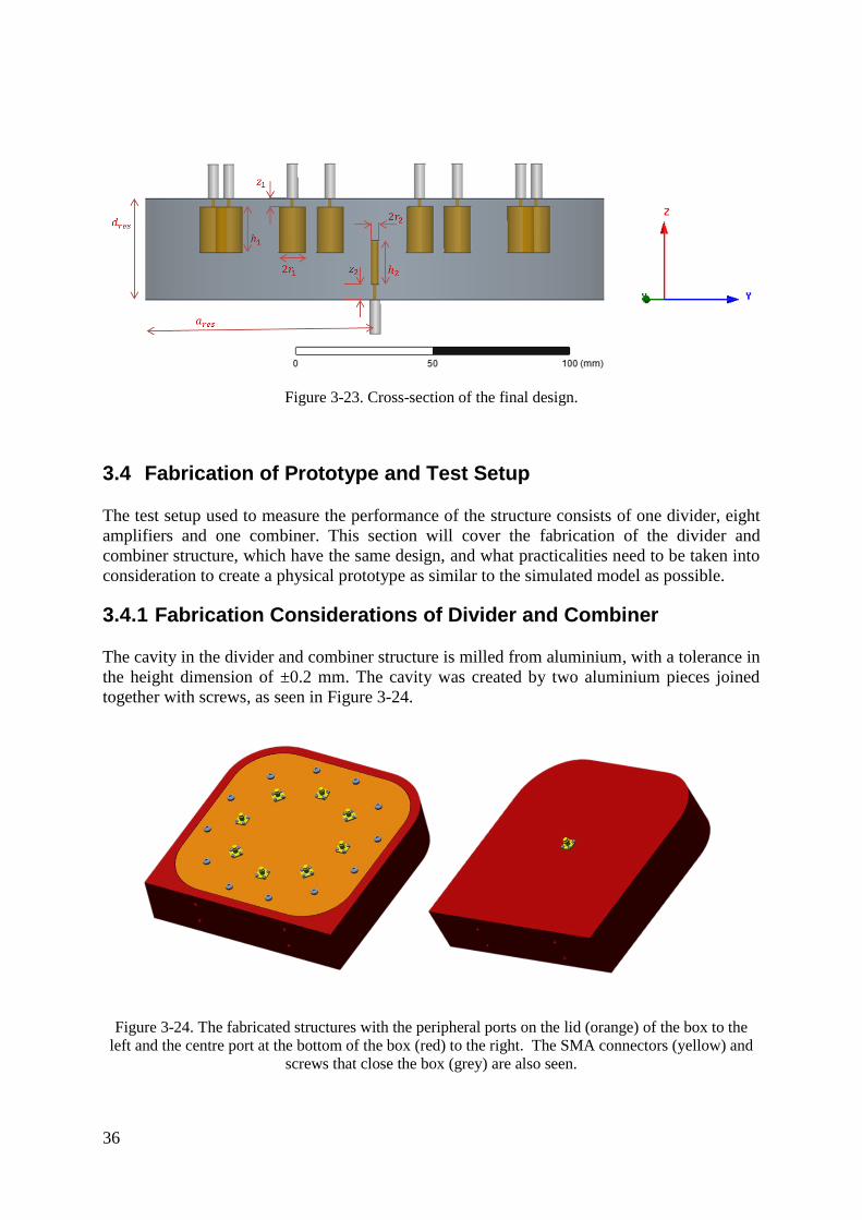
36
Figure 3-23. Cross-section of the final design.
3.4 Fabrication of Prototype and Test Setup
The test setup used to measure the performance of the structure consists of one divider, eight
amplifiers and one combiner. This section will cover the fabrication of the divider and
combiner structure, which have the same design, and what practicalities need to be taken into
consideration to create a physical prototype as similar to the simulated model as possible.
3.4.1 Fabrication Considerations of Divider and Combiner
The cavity in the divider and combiner structure is milled from aluminium, with a tolerance in
the height dimension of ±0.2 mm. The cavity was created by two aluminium pieces joined
together with screws, as seen in Figure 3-24.
Figure 3-24. The fabricated structures with the peripheral ports on the lid (orange) of the box to the
left and the centre port at the bottom of the box (red) to the right. The SMA connectors (yellow) and
screws that close the box (grey) are also seen.

37
The joint between the aluminium part containing the cavity and the aluminium lid that closes
the cavity was positioned where the conducting surface surrounding the cavity has low
surface currents. This choice was made to minimize disturbance of the field within the cavity
and to prevent electrical leakage.
Figure 3-25 shows the surface currents on the cylindrical cavity. With regard to this and
practical aspects in the assembling of the test setup, a design where the cylindrical cavity is
milled in a piece of aluminium and closed with an aluminium lid that was screwed onto the
cavity was chosen.
Figure 3-25. Surface currents plotted on the cylindrical cavity. The upper corner is of special interest
as it is the place for the junction in the fabricated prototype.
The metallic, cylindrical box and the lid are shown in Figure 3-26. To prevent radiation to
leak from the cavity, the gap around the lid is shifted a few mm from the cavity walls, as seen
in Figure 3-26. This prevents radiation leakage in the event of a un-tight lid.
Figure 3-26. The cylindrical cavity box and the lid, both in aluminium, surrounding the cavity that the
divider and combiner are based on.

38
3.4.2 Fabrication of SMA Connector Probe Modifications
The SMA connectors were purchased with a standard radius and length of the coaxial centre
pin, and custom made copper cylinders were designed to be soldered onto the pins by hand.
Each cylinder has a drilled hole with a certain depth to help fixate the cylinder at the correct
distance from the cavity lid, to simplify the soldering. An air valve at the bottom of the hole is
also added to make it easier to get the solder into the hole.
The size of the copper cylinder in combination with the manual assembly of the probe
modifications complicates the fabrication, and it is hard to predict the uncertainties. In Figure
3-27, the measurements and tolerances of the probe modifications are displayed. The outer
measurements are also found in Table 3-1 on page 35.
Figure 3-27. Measurements and tolerances of the copper cylinders used for probe modification. The
left cylinder is the centre port modification to the connectors at port 1-8 and the right cylinder is the
peripheral port modification to the connector at port 9.
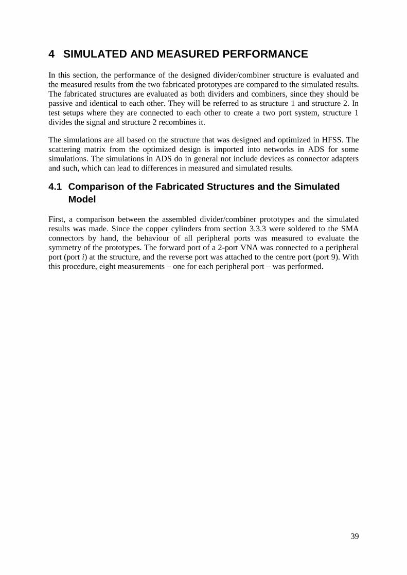
39
4 SIMULATED AND MEASURED PERFORMANCE
In this section, the performance of the designed divider/combiner structure is evaluated and
the measured results from the two fabricated prototypes are compared to the simulated results.
The fabricated structures are evaluated as both dividers and combiners, since they should be
passive and identical to each other. They will be referred to as structure 1 and structure 2. In
test setups where they are connected to each other to create a two port system, structure 1
divides the signal and structure 2 recombines it.
The simulations are all based on the structure that was designed and optimized in HFSS. The
scattering matrix from the optimized design is imported into networks in ADS for some
simulations. The simulations in ADS do in general not include devices as connector adapters
and such, which can lead to differences in measured and simulated results.
4.1 Comparison of the Fabricated Structures and the Simulated
Model
First, a comparison between the assembled divider/combiner prototypes and the simulated
results was made. Since the copper cylinders from section 3.3.3 were soldered to the SMA
connectors by hand, the behaviour of all peripheral ports was measured to evaluate the
symmetry of the prototypes. The forward port of a 2-port VNA was connected to a peripheral
port (port i) at the structure, and the reverse port was attached to the centre port (port 9). With
this procedure, eight measurements – one for each peripheral port – was performed.

40
4.1.1 Scattering parameters
The resulting scattering parameters from the measurements are displayed in Figure 4-1 and
Figure 4-2. The corresponding scattering parameters for the simulated model are displayed in
Figure 4-3, and are nearly perfectly symmetric. The variation is a result of the simulation
method and the choice of mesh in HFSS. The measured reflection coefficient at the peripheral
ports, 𝑆𝑖𝑖, varies within a range of 5 dB for structure 1 and 12 dB for structure 2, which means
that the structure is not very symmetric, which might affect the field in the cavity. The
coupling 𝑆𝑖9 ≈ 𝑆9𝑖 should ideally be -9.03 dB but varies between -9.41 dB and -8.85 dB for
structure 1 and -9.50 dB and -9.03 dB for structure 2 for the frequency band of 2.9 GHz to 3.3
GHz. This means that the division of power would not be symmetric for these structures. The
reflection coefficient at the centre port 𝑆99 is measured in eight identical measurements – one
for each measurement of the peripheral ports – and is -16.25 dB for structure 1 and -14.83 dB
for structure 2.
A comparison of the performance of the measured structures and the simulated design is done
in section 4.1.2 below.
Figure 4-1. Measured scattering parameters of Structure 1. The reflection coefficient Sii at the
peripheral ports is less than -16.7 dB for all ports while the reflection coefficient at the centre port S99
is less than -16.3 dB for 2.9 GHz-3.3 GHz. The coupling parameters S21 andS12 varies between -9.4 dB
and -8.4 dB.
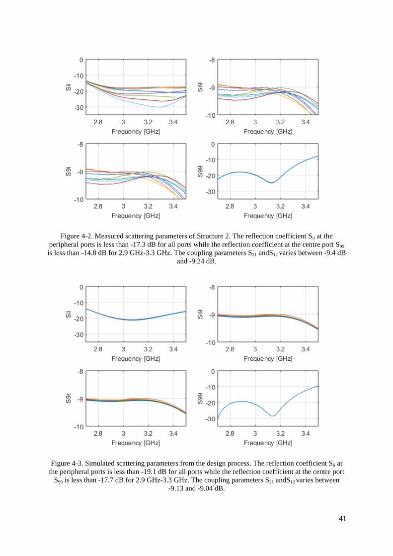
41
Figure 4-2. Measured scattering parameters of Structure 2. The reflection coefficient Sii at the
peripheral ports is less than -17.3 dB for all ports while the reflection coefficient at the centre port S99
is less than -14.8 dB for 2.9 GHz-3.3 GHz. The coupling parameters S21 andS12 varies between -9.4 dB
and -9.24 dB.
Figure 4-3. Simulated scattering parameters from the design process. The reflection coefficient Sii at
the peripheral ports is less than -19.1 dB for all ports while the reflection coefficient at the centre port
S99 is less than -17.7 dB for 2.9 GHz-3.3 GHz. The coupling parameters S21 andS12 varies between
-9.13 and -9.04 dB.

42
4.1.2 Return and Insertion Loss
The fabricated structures had identical designs which are passive and reciprocal, which means
that they should be able to operate as both a divider and a combiner. The return loss (RL) and
insertion loss (IL) was therefore calculated both when the peripheral ports acted as input ports
and when the structure was excited at the centre port.
Figure 4-4 displays the return loss and insertion loss for the structures and the simulated
model when they are used as combiners. That is, the return loss is calculated for each
individual peripheral port from its 𝑆𝑖𝑖 parameter and the displayed value in Figure 4-4 is the
average of the eight calculated return loss values. The measured return loss of the fabricated
structures show a wider bandwidth than the return loss from the simulated model. The pass
band is however shifted towards higher frequency, and has a centre frequency around 3.3
GHz, which is 0.2 GHz higher than the design frequency and means a shift in centre
frequency of 6 %. Structure 1 has a RL=18 dB bandwidth of 0.8 GHz around 3.3 GHz which
gives a bandwidth of 24 %. Structure 2 has a RL=19 dB bandwidth of 0.7 GHz around 3.2
GHz which gives a bandwidth of 21 %.
The insertion loss, however, is shifted by 6 % towards lower frequencies with centre
frequency around 2.9 GHz, compared to design frequency of 3.1 GHz. Structure 1 has an IL=
0.20 dB bandwidth of 0.6 GHz around 2.9 GHz which gives a bandwidth of 22 %. Structure 2
has an IL=0.25 dB bandwidth of 0.7 GHz around 2.9 GHz which gives a bandwidth of 23 %.
Figure 4-4. Average peripheral port return loss and insertion loss for the structures. The measured
return loss of the structures shows a more broadband behaviour than the simulated values.
Figure 4-5 displays the return loss and insertion loss for when the structures and simulated
model is used as a divider. The peaks in the return loss for the measurements follow the
simulation well, while structure 1 shows slightly better performance in return loss for the
lower design frequencies. Structure 1 has a RL=16 dB bandwidth of 0.7 GHz around 2.9 GHz
which gives a bandwidth of 24 %.
A better RL performance can be achieved if the highest 0.05 GHz of the design frequencies
are excluded from the design requirements; RL>19 dB is found for 2.61-3.25 GHz. Structure
2 has a RL=15 dB bandwidth of 0.7 GHz around 2.9 GHz which gives a bandwidth of 24 %.

43
As in the case with structure 2, a better RL can be achieved if the highest design frequencies
are excluded from the passband; RL>17 dB for 2.60-3.25 GHz.
The insertion loss for the divider and combiner application should be identical according to
theory and simulation. The measured result is consistent with theory.
Figure 4-5. Centre port return loss and insertion loss for the structures. The simulated result show
smaller insertion loss than the measurement, while the measured centre port return loss behaviour is
very similar to the simulation.
4.1.3 Leakage and Isolation
For the measurement of isolation between peripheral ports, a peripheral port of each structure
was chosen as reference, called port 1. The ports with the behaviour closest to average
behaviour were chosen, and the remaining peripheral ports were numbered as in Figure 4-6.
Figure 4-6. Numbering of the peripheral ports, ports 1-8. The centre port on the opposite side of the
cavity is port number 9.
The measured leakage between port 1 and the other peripheral ports for structure 1 and
structure 2 is displayed in Figure 4-7 together with the simulated values. From the simulated
values, it is seen that port 1 couples strongest with its opposite port, port 5, and the neighbour
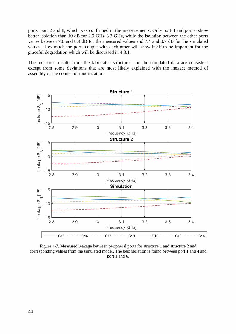
44
ports, port 2 and 8, which was confirmed in the measurements. Only port 4 and port 6 show
better isolation than 10 dB for 2.9 GHz-3.3 GHz, while the isolation between the other ports
varies between 7.8 and 8.9 dB for the measured values and 7.4 and 8.7 dB for the simulated
values. How much the ports couple with each other will show itself to be important for the
graceful degradation which will be discussed in 4.3.1.
The measured results from the fabricated structures and the simulated data are consistent
except from some deviations that are most likely explained with the inexact method of
assembly of the connector modifications.
Figure 4-7. Measured leakage between peripheral ports for structure 1 and structure 2 and
corresponding values from the simulated model. The best isolation is found between port 1 and 4 and
port 1 and 6.
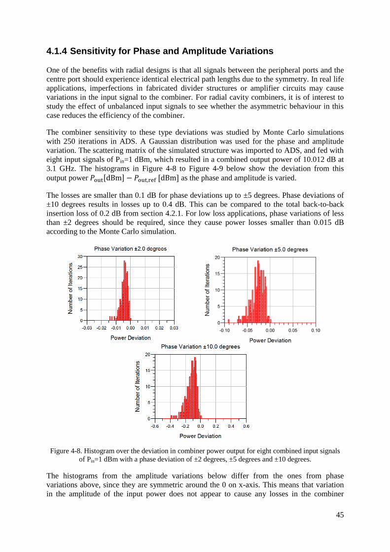
45
4.1.4 Sensitivity for Phase and Amplitude Variations
One of the benefits with radial designs is that all signals between the peripheral ports and the
centre port should experience identical electrical path lengths due to the symmetry. In real life
applications, imperfections in fabricated divider structures or amplifier circuits may cause
variations in the input signal to the combiner. For radial cavity combiners, it is of interest to
study the effect of unbalanced input signals to see whether the asymmetric behaviour in this
case reduces the efficiency of the combiner.
The combiner sensitivity to these type deviations was studied by Monte Carlo simulations
with 250 iterations in ADS. A Gaussian distribution was used for the phase and amplitude
variation. The scattering matrix of the simulated structure was imported to ADS, and fed with
eight input signals of Pin=1 dBm, which resulted in a combined output power of 10.012 dB at
3.1 GHz. The histograms in Figure 4-8 to Figure 4-9 below show the deviation from this
output power 𝑃out[dBm] − 𝑃out,ref [dBm] as the phase and amplitude is varied.
The losses are smaller than 0.1 dB for phase deviations up to ±5 degrees. Phase deviations of
±10 degrees results in losses up to 0.4 dB. This can be compared to the total back-to-back
insertion loss of 0.2 dB from section 4.2.1. For low loss applications, phase variations of less
than ±2 degrees should be required, since they cause power losses smaller than 0.015 dB
according to the Monte Carlo simulation.
Figure 4-8. Histogram over the deviation in combiner power output for eight combined input signals
of Pin=1 dBm with a phase deviation of ±2 degrees, ±5 degrees and ±10 degrees.
The histograms from the amplitude variations below differ from the ones from phase
variations above, since they are symmetric around the 0 on x-axis. This means that variation
in the amplitude of the input power does not appear to cause any losses in the combiner

46
structure, and the outcome of the Monte Carlo simulation corresponds to the variation of the
input power.
Figure 4-9. Histogram over the deviation in combiner power output for eight combined input signals
of Pin=1±0.1 dBm, Pin=1±0.5 dBm and Pin=1±1 dBm.
4.2 Characteristics of Divider Connected to Combiner
A passive setup where structure 1 was used as a divider and structure 2 was used as a
combiner was tested, to study the performance of the two structures like they are used in an
amplifier system. The two structures were connected back-to-back, which means that they
were connected to each other through their peripheral ports via SMA-adapters. The centre
port at structure 1 was assigned to be port 1 and the centre port at structure 2 was assigned to
be port 2. Since no adapters were included in the simulation, it was expected that reflections
at additional frequencies could occur in the measurements compared to the simulation.

47
Figure 4-10. Back-to-back setup, where the peripheral ports of the two structures are connected
through SMA-adapters
4.2.1 Scattering Parameters
The measured and the simulated results for the back-to-back setup are compared in Figure
4-11 below. The simulated and measured results have similar behaviours, but there seems to
be a shift in frequency for the measured results compared to the simulated ones. A number of
additional peaks are introduced in the measurements compared to the simulation, while the
two significant peaks between 2.5 GHz and 2.8 GHz in the simulation are absent in the
measurement. The reflection losses are higher in the measured data for the design frequencies,
and the transmission losses between port 1 and port 2 increases from 0.05 dB to 0.28 dB at 3.1
GHz.
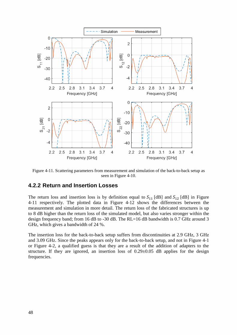
48
Figure 4-11. Scattering parameters from measurement and simulation of the back-to-back setup as
seen in Figure 4-10.
4.2.2 Return and Insertion Losses
The return loss and insertion loss is by definition equal to 𝑆11 [dB] and 𝑆12 [dB] in Figure
4-11 respectively. The plotted data in Figure 4-12 shows the differences between the
measurement and simulation in more detail. The return loss of the fabricated structures is up
to 8 dB higher than the return loss of the simulated model, but also varies stronger within the
design frequency band; from 16 dB to -30 dB. The RL=16 dB bandwidth is 0.7 GHz around 3
GHz, which gives a bandwidth of 24 %.
The insertion loss for the back-to-back setup suffers from discontinuities at 2.9 GHz, 3 GHz
and 3.09 GHz. Since the peaks appears only for the back-to-back setup, and not in Figure 4-1
or Figure 4-2, a qualified guess is that they are a result of the addition of adapters to the
structure. If they are ignored, an insertion loss of 0.29±0.05 dB applies for the design
frequencies.
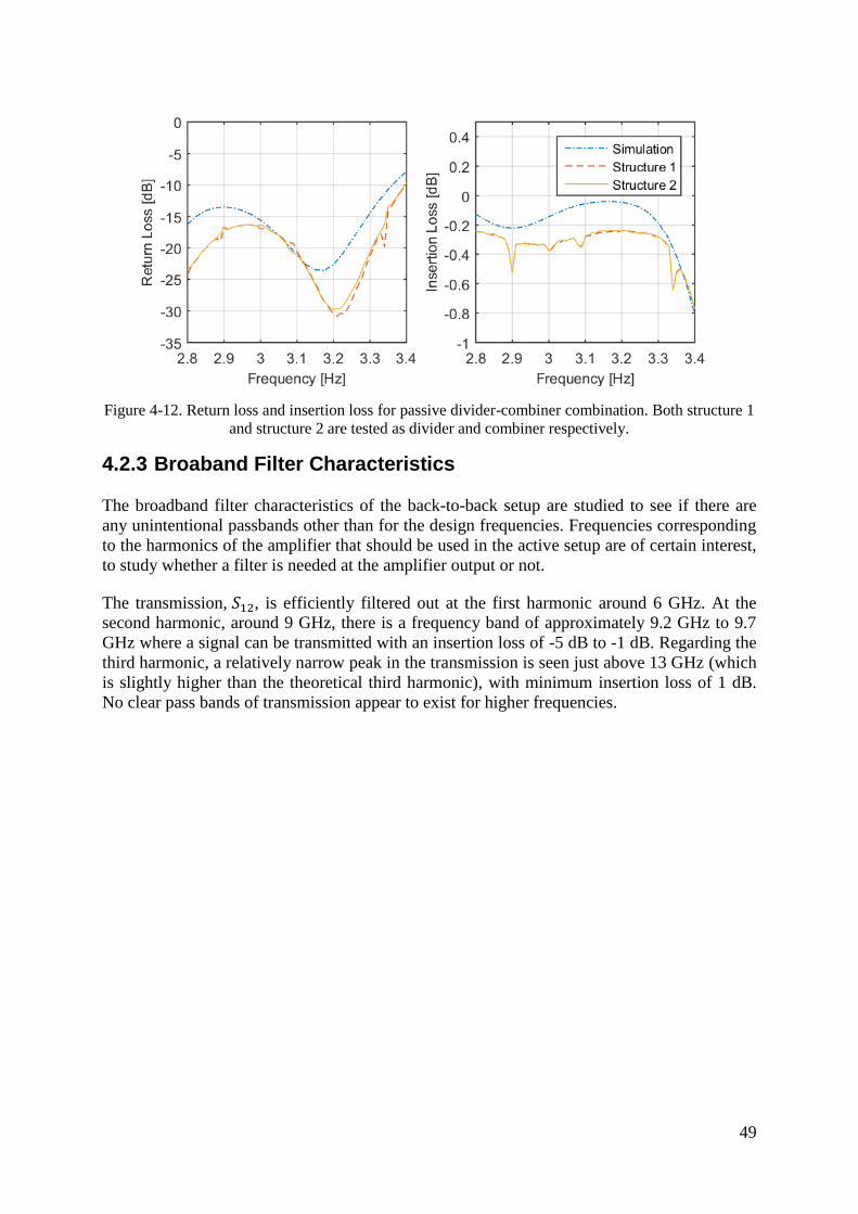
49
Figure 4-12. Return loss and insertion loss for passive divider-combiner combination. Both structure 1
and structure 2 are tested as divider and combiner respectively.
4.2.3 Broaband Filter Characteristics
The broadband filter characteristics of the back-to-back setup are studied to see if there are
any unintentional passbands other than for the design frequencies. Frequencies corresponding
to the harmonics of the amplifier that should be used in the active setup are of certain interest,
to study whether a filter is needed at the amplifier output or not.
The transmission, 𝑆12, is efficiently filtered out at the first harmonic around 6 GHz. At the
second harmonic, around 9 GHz, there is a frequency band of approximately 9.2 GHz to 9.7
GHz where a signal can be transmitted with an insertion loss of -5 dB to -1 dB. Regarding the
third harmonic, a relatively narrow peak in the transmission is seen just above 13 GHz (which
is slightly higher than the theoretical third harmonic), with minimum insertion loss of 1 dB.
No clear pass bands of transmission appear to exist for higher frequencies.
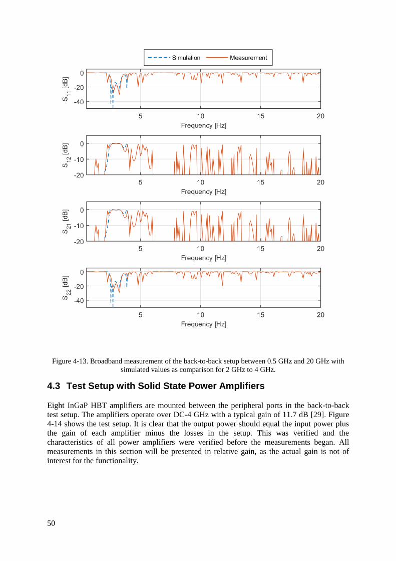
50
Figure 4-13. Broadband measurement of the back-to-back setup between 0.5 GHz and 20 GHz with
simulated values as comparison for 2 GHz to 4 GHz.
4.3 Test Setup with Solid State Power Amplifiers
Eight InGaP HBT amplifiers are mounted between the peripheral ports in the back-to-back
test setup. The amplifiers operate over DC-4 GHz with a typical gain of 11.7 dB [29]. Figure
4-14 shows the test setup. It is clear that the output power should equal the input power plus
the gain of each amplifier minus the losses in the setup. This was verified and the
characteristics of all power amplifiers were verified before the measurements began. All
measurements in this section will be presented in relative gain, as the actual gain is not of
interest for the functionality.

51
Figure 4-14. Schematic view of the active test setup where the peripheral ports of the structure are
connected to solid state power amplifiers. The overall increase in Pout should be equal to the amplifier
gain, G dB.
4.3.1 Graceful Degradation in the Event of Amplifier Failure
The measurement of graceful degradation was performed as follows: a reference measurement
of 𝑆12 was done when all amplifiers were biased. After that, the bias was removed from one
or more amplifier to imitate amplifier failure and the new 𝑆12 was measured. The results
presented in Figure 4-15, Figure 4-16 and Figure 4-17 all show the change in gain that this
results in.
Figure 4-15 shows the results for when the amplifiers are in their linear region. This means
that when the power that should have gone through the unbiased amplifier is reflected and
flows through other peripheral ports than the “failed” one, it may still get amplified and
combined together with the rest of the output signal. In Figure 4-16, on the other hand, the
amplifiers have been driven into compression so that the output from the amplifier is limited
at its saturated output power. The result of this is that it does not matter if the power from a
failed port is reflected and inserted into other amplifiers, since they are already at their
maximum output power level. This can be seen when the results in Figure 4-15 and Figure
4-17 are compared.
The average power loss for 1-port failure in the saturated case results in a power loss of
around 1.8 dB in average while the same scenario with amplifiers in the linear region results
in a power loss of around 1.3 dB in average. The same difference for 2-port failures gives an
average power loss of approximately 4 dB in the saturated case and 3 dB in the case where the
amplifier operates in its linear region. It is clear from the measurements that the loss varies
heavily with frequency, even over the relatively short band of design frequencies, 2.9 GHz to
3.3 GHz. The shape of the 1 port-loss curves are similar in the linear and saturated case, but
the measurement from the saturated amplifiers appears to be shifted with approximately 50
MHz. This tendency is also seen in the 2-port failure data, but cannot be observed as clearly in
the 3-port failure case since the saturated 3-port failure data does not have as noticeable
peaks. The unevenness of the curve is discussed further in section 4.3.2.
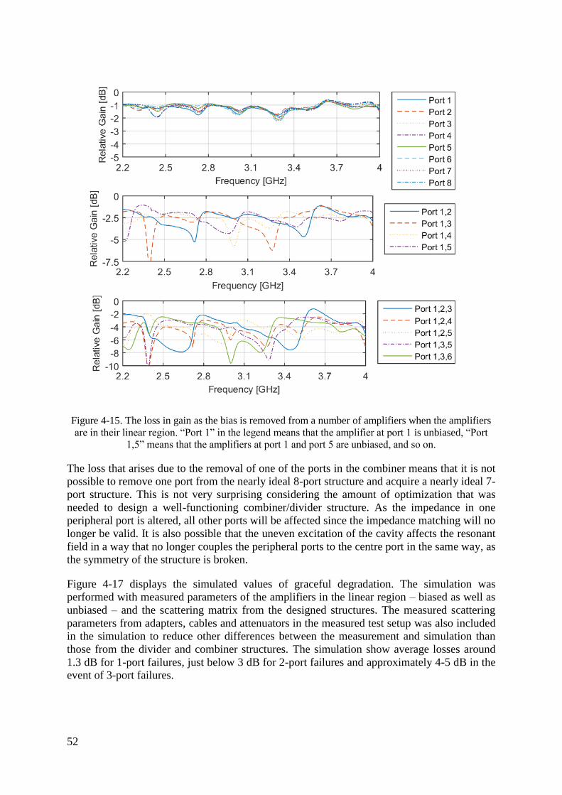
52
Figure 4-15. The loss in gain as the bias is removed from a number of amplifiers when the amplifiers
are in their linear region. “Port 1” in the legend means that the amplifier at port 1 is unbiased, “Port
1,5” means that the amplifiers at port 1 and port 5 are unbiased, and so on.
The loss that arises due to the removal of one of the ports in the combiner means that it is not
possible to remove one port from the nearly ideal 8-port structure and acquire a nearly ideal 7-
port structure. This is not very surprising considering the amount of optimization that was
needed to design a well-functioning combiner/divider structure. As the impedance in one
peripheral port is altered, all other ports will be affected since the impedance matching will no
longer be valid. It is also possible that the uneven excitation of the cavity affects the resonant
field in a way that no longer couples the peripheral ports to the centre port in the same way, as
the symmetry of the structure is broken.
Figure 4-17 displays the simulated values of graceful degradation. The simulation was
performed with measured parameters of the amplifiers in the linear region – biased as well as
unbiased – and the scattering matrix from the designed structures. The measured scattering
parameters from adapters, cables and attenuators in the measured test setup was also included
in the simulation to reduce other differences between the measurement and simulation than
those from the divider and combiner structures. The simulation show average losses around
1.3 dB for 1-port failures, just below 3 dB for 2-port failures and approximately 4-5 dB in the
event of 3-port failures.

53
Figure 4-16. The loss in gain as the bias is removed from a number of amplifiers when the amplifiers
are saturated. “Port 1” in the legend means that the amplifier at port 1 is unbiased, “Port 1,5” means
that the amplifiers at port 1 and port 5 are unbiased, and so on.
The results agree with the measured results in the linear region. The simulated values are far
more cohesive than the measured values, and since it is known from previous measurements
that the peripheral ports suffer from asymmetry in the measured structures, it is a likely reason
why.
From both the measurements and simulation, it is clear that failure of some ports or
combinations of ports generate more losses than other – although it is much more obvious
differences in the measured cases. One of the goals with the simulation and measurements
was to understand why some cases offer a more graceful degradation than other and one
hypothesis was that it could depend on the coupling between peripheral ports. It is hard to
draw any conclusions from the results as they vary very much in frequency and since the
simulated curves are so much flatter than the measured ones.

54
Figure 4-17. The simulated losses in gain as an amplifier taken out of operation. “Port 1” in the legend
means that the amplifier at port 1 is unbiased ,“Port 1,5” means that the amplifiers at port 1 and port 5
are unbiased, and so on.
In conclusion, it can be stated that the loss that arises due to the removal of one of the ports in
the combiner means that it is not possible to remove one port from the nearly ideal 8-port
structure and acquire a nearly ideal 7-port structure. This is not very surprising considering
the amount of optimization that was needed to design a well-functioning combiner/divider
structure. As the impedance in one peripheral port is altered, all other ports will be affected
since the impedance matching will no longer be valid. It is also possible that the uneven
excitation of the cavity affects the resonant field in a way that changes the coupling of the
peripheral ports to the centre port.
4.3.2 Methods for Improvement of Graceful Degradation
Even though graceful degradation is far better than total failure of an amplifier network if one
of the constituent components fail, failure of one or more amplifiers still leads to a severe
impairment of the functionality of the network. According to Ernst, Camisa and Presser [32]
the decrease of output power for N-way combiners can be calculated as
𝑃𝑜𝑢𝑡
𝑃𝑜𝑢𝑡,𝑚𝑎𝑥= [√𝑘 +
𝑀
𝑁(1 − √𝑘)] 2 (4.1)

55
where 𝑘 is the fractional output of a failing amplifier, which varies between 0 and 1
depending on whether the amplifier fails entirely or not. 𝑀 is the number of functioning
amplifiers and 𝑁 is the number of ports in the combiner network. For an 8-port combiner with
one totally failed amplifier, (4.1) gives an output power of 77 % of the maximum output,
which translates into a loss of 1.16 dB. The corresponding values for two failed amplifiers are
56 % and 2.5 dB and for three failed amplifiers: 40 % and 4 dB. This corresponds well to the
measured and simulated results from the previous sections.
These theories are traditionally applied on tree structure combiner networks, which differ
from the cavity combiners in their principle of construction. In this master thesis project, one
of the aims was to study if there was a way to improve the graceful degradation by
modification of the failed or remaining ports. In the event of one failed amplifier, it is a matter
of trying to readjust the properties of the combiner so that it behaves more like a 7-way
combiner than an 8-way combiner when it fails. This was done in the software ADS by
replacement of one amplifier with different components or terminations according to the
sketch in Figure 4-18.
Figure 4-18. Network for test of methods for improvement of the graceful degradation. The box with
the question mark was replaced with different type of terminations and components.
The removed amplifier model was replaced with open circuit, short circuit, a short circuit with
an equation based 2-port Z-parameter component, a phase shifter, the scattering matrix
measured from one unbiased amplifier and a combination of the latter and two equation based
2-port Z-parameter component – one at the input and one at the output ports of the scattering
matrix. The circuits with the phase shifter and the Z-parameter components were optimized
for maximum 𝑆21between 2.9 GHz and 3.3 GHz and the resulting parameters are listed in the
legend in Figure 4-19.
Figure 4-19 displays the resulting relative losses. It is clear from the results that different
replacements for a faulty amplifier can change the graceful degradation for certain
frequencies significantly. For example, to replace the amplifier with an open circuit leads to
losses larger than 3 dB for some frequencies while a short circuit results in losses barely
above 1 dB at the most, and with a more even behaviour over frequencies. The optimizations
performed with the phase shifter and the Z-parameter components did not result in large
improvements, but still affects the performance.

56
Figure 4-19. Result of the test of different ways to improve the graceful degradation. The best result
for 2.9 GHz to 3.3 GHz is achieved when the failed amplifier is replaced with a phase shift of 15°.
Some tests to optimize different components at the remaining ports instead of the failed one
was performed, but only for a passive combiner setup. That did not result in any successful
improvements, but it could still be of interest to study possible optimizations further for the
setup used in Figure 4-18, with the goal to find easy way to re-match the structures to behave
more like (N-1)-way dividers and combiners in the event of a port failure.

57
5 DISCUSSION AND FURTHER WORK
5.1 Radial Power Combiner as an Alternative for Combiner
Networks
The radial power combiner is very interesting as concept, as it is a relatively simple and
robust way to realize high power generation with low losses. It has been investigated since the
second half of the 20th
century, but is despite this a relatively unknown and unused type of
technology that may have many applications as the solid state power amplifiers continue to
show increasing performance at high power levels.
5.2 Construction of Radial Cavity Power Combiners in General
In section 3.1, a study of the construction of a cylindrical cavity radial power combiner was
presented. The aim of the study was not to go into detail of every design parameter as they
change depending on the technology used to realize the cavity combiner. However, the goal
was to give an idea about what challenges need to be dealt with in the design process, and
what design considerations that need to be made in the beginning of a design process. In
conclusion, there are four questions that one could ask oneself when designing a radial cavity
combiner:
1. How many signals should be combined?
2. Are there any restrictions regarding choice of port interfaces?
3. How can the impedance for the different parts in the combiner be tuned?
4. Will there be need for additional isolation?
Some areas in the conceptual study should be studied further to get a better understanding of
the construction, and most important of these are the restriction regarding number of
peripheral ports and their positions. The number of ports is closely related to the bandwidth of
a cavity combiner, but is also dependent on the required power level for the design.
Another interesting part of the construction is the isolation in a cavity combiner, which in all
essential comes down to mode suppression of resonant modes in cylindrical cavities. Both the
need of isolation and suitable ways to realize them are of interest. Usual tools for mode
suppression such as slits where unwanted waves can radiate out or thin metal walls to block
waves can be problematic in high power application.
5.3 Evaluation of the Design, Fabrication and Verification of the 8-
Way Cavity Combiner/Divider Structures
All simulations and optimizations of the designed structures were performed in HFSS with all
metal surfaces assigned as perfect electrical conducting surfaces and the cavity was assigned
as vacuum. Apart from this, the only other material used in the simulations was the Teflon in
the SMA connectors. When the fabrication of the combiner/divider structures was about to be
initialized, a number of control simulations were performed. This included simulations of
tolerances, possible leakage in joints and simulations of materials such as air, aluminium and

58
beryllium brass. None of these factors were considered to have high enough impact to be
taken into consideration in the optimizations.
The copper cylinders that were used to modify the SMA connectors are the largest source of
uncertainty in the realisation of the design. A large effort was made to simplify the assembly
of them so that the result would be as precise as possible, and the prepared holes in the copper
cylinders were designed to help fixating them in the correct positions. It was, despite this,
hard to mount them identically and the incoherence in the reflection coefficient at the
peripheral ports is most likely a result of this. The measured peripheral port return loss for the
structures showed a significantly broader band than the simulation had predicted. This might
be a result of the imperfect realization of the peripheral probe modifications.
The optimization of the probes and the cavity height gave satisfactory results, but the
frequency bands with good matching at the peripheral and centre ports did not coincide. It
would have been of interest to know if anything could have been done to have the best
performance at both ports simultaneously without any trade-off with other design
requirements. In order to get to the bottom of this, a more detailed analysis of the behaviour of
the connector probe modifications needs to be performed.
5.4 Recommended Future Work
There are three main areas where further work would be recommended:
Study of number of peripheral ports for cavity combiners and other types of radial
combiners. Matsumura and Mizuno [9] discuss how the number of ports in a cavity
combiner is related to the bandwidth and the choice of resonant mode for the cavity
resonator, and their article is a good starting point for further work.
Transformation of the cylindrical TM0m0 mode to a rectangular waveguide TE10 mode
that would be of interest for the radar application. This is done in a number of
published papers (see Table 2-3 for examples), but was not successfully done in this
thesis work. A waveguide transducer could be used, but a probe that is excited by the
cylindrical cavity and feeds the rectangular waveguide is another interesting option to
study.
Further studies of how the graceful degradation could be improved for different types
of radial N-way combiners, with focus on how an N-way combiner can be modified
into an (N-1)-way combiner in the event of port failure. It would be interesting to
study how the reflected power from a failed port is distributed between the remaining
ports, and how the matching of the remaining ports is affected. If the principle behind
this is understood, it might be possible to draw conclusions about how the combiner
should be modified to improve the graceful degradation.
5.5 Ethical Aspects and a Sustainability Perspective of the Radial
Power Combiner/Divider
The radial power combiner/divider is used in the amplifier step of an RF system to generate
high output power for satellite and radar applications. The technology would fill the same
purpose that travelling wave tubes do today, meaning that there would likely not be any
ethical consequences to consider regarding new innovations or applications of the technology.
59
An obvious advantage of amplifier systems based on SSPAs and radial power
combiner/divider structures is the graceful degradation. When the technology is used in
satellites for example, or research projects, it is not always possible to replace broken parts
and failure of for example the TWTA could be the end of an experiment in space. If the
output power is enough in the event of graceful degradation with an SSPA based
amplification step, resources could be spared both financially and environmentally. The
design of most combiner-based amplifier solutions is also constructed in a way that a
minimum number of parts need to be exchanged in the event of failure which is also a
responsible use of resources such as rare metals.
One application of the radial power combiner/divider is in military radar systems. The
defence industry is not uncontroversial, and every technical invention in the area can be used
in offence as well as defence. Radar systems can be used to detect threats and to support the
elimination of them, but could also be used to detect targets and attack them. It is of course a
subjective matter to decide who is suited to have weapons and other military equipment and
why. These are very generic discussions and the technology of the SSPA and radial power
combiner/divider system are not that specific to the area of application that these ethical
aspects need to be considered. It is more correct to compare it to for example a bolt in a band
waggon – it may be an essential part for the band waggons function, but it is also an essential
part in many other uncontroversial inventions such as buildings, cars and Ferris wheels, and
should therefore not be the subject for the ethical discussions surrounding the military
industry.
60
6 CONCLUSION
The construction of a cylindrical cavity combiner/divider for the TM020 mode was analysed
and a prototype 8-way combiner/divider structure was designed and fabricated. The most
crucial part of the design process was the impedance matching at the different ports to reduce
losses in the system. The measured average return loss for the peripheral ports is higher than
18.4 dB and the measured centre port return loss higher than 17.6 dB for a 10 % bandwidth
around the centre design frequency of 3.1 GHz. The measured insertion loss is lower than
0.16 dB for the same band.
Uncoherent phase of the input power in a structure used as a combiner resulted in simulated
losses; a phase variation of ±2 degrees in the input signals caused loss in the combined power
as large as 0.015 dB, while a phase variation of ±5 degrees caused loss up to 0.1 dB, which is
in the same size of the insertion loss. The combined output power was however unaffected by
deviations in the amplitude of the input power.
The back-to-back structure showed decent filter characteristics but had tendencies to pass
harmonics around 9.3 GHz.
The graceful degradation followed the theoretical model with some additional loss for the
measurements and varied with frequency. Different methods to improve the graceful
degradation were studied and improvements could be observed in some cases, but further
studies are needed to draw any general conclusions.

61
BIBLIOGRAPHY
[1] R. Danieli and R. Giofré, “Development of High Efficiency and High LInearity Power
Amplifiers for Space Applications,” IEEE MTT-S Graduate Fellowship Project Report.
[2] A. Leggieri, G. Orengo, D. Passi and F. D. Paolo, “The Squarax Spatial Power
Combiner,” Progress In Electromagentics Research C, vol. 45, pp. 43-55, 2013.
[3] R. Giofré, P. Colantonio, E. Cipriani, F. Gianni, L. Gonzalez, F. D. Arriba and L. Cabria,
“A High-Power Solid State Amplifier for Galileo Satellite System Exploiting European
GaN Technology,” International Journal of Microwave and Wireless Technologies,
Cambrigde, 2016.
[4] K. J. Russel, “Microwave Power Combining Techniques,” IEEE Transactions on
Microwave Theory and Techniques, Vols. MTT-27, no. 5, pp. 472-478, 1979.
[5] C. G. Montgomery, R. H. Dicke and E. M. Purcell, Principles of Microwave Circuits,
London: Peter Peregrinus Ltd., 1987.
[6] R. F. Harrington, Time Harmonic Electromagnetic Fields, New York: McGraw-Hill
Book Company Inc., 1961.
[7] D. M. Pozar, Microwave Engineering, 4 ed., Oxford, UK: John Wiley & Sons, Inc, 2011.
[8] R. E. Collin, Foundations for Microwave Engineering, Hoboken: Wiley-IEEE Press,
2001.
[9] H. Matsumura and H. Mizuno, “Design of Microwave Power Combiner with Circular
TM0m0 Mode Cavity,” Electronics and Communications in Japan, Part 2, vol. 70, no. 9,
1987.
[10] M. Ghanadi, “A New Compact Broadband Radial Power Combiner,” der Technischen
Universität Berlin, Berlin, 2012.
[11] R. Aston, “Techniques for Increasing the Bandwidth of a TM010-Mode Power
Combiner,” IEEE Transactions on Microwave Theory and Techniques, Vols. MTT-27,
no. 5, pp. 479-482, 1979.
[12] Y. Tokumitsu, T. Saito, N. Okubo and Y. Kaneko, “A 6-GHz 80-W GaAs FET Amplifier
with a TM-Mode Cavity Power Combiner,” IEEE Transactions on Microwave Theory
and Techniques, Vols. MTT-32, no. 3, pp. 301-308, 1984.
[13] E. Belohoubek, R. Brown, H. Johnson, A. Fathy, D. Bechtle, D. Kalokitis and E.
Mykietyn, “30-Way Radial Power Combiner for Miniature GaAs FET Power
Amplifiers,” IEEE MTT-S International Microwave Symposium Digest, pp. 515-518,

62
1986.
[14] K. Song, Y. Fan and Y. Zhang, “Eight-Way Substrate Integrated Waveguide Power
Divider With Low Insertion Loss,” IEEE Transactions on Microwave Theory and
Techniques, vol. 56, no. 6, pp. 1473-1477, 2008.
[15] A. Jain, A. K. Gupta, D. K. Sharma, P. R. Hannurkar and S. K. Pathak, “Design and
Analysis of a High-Power Radial Multi-Way Combiner,” International Journal of
Microwave and Wireless Technologies, vol. 6, no. 1, pp. 83-91, 2014.
[16] K. Wu, D. Deslandes and Y. Cassivi, “The Substrate Integrated Circuits - A New
Concept For High- Frequency Electronics and Opto-Electronics,” in In proceedings of
IEEE Telecommunications in Modern Satellite, Cable and Broadcasting Service, Serbia
Montenegro, 2003.
[17] J. M. Denoual, A. Peden, B. Della and J.-P. Fraysse, “16-Way Radial Divider/Combiner
for Solid State Power Amplifiers in the K-band,” in Proceedings of IEEE 38th European
Microwave Conference , Amsterdam, Netherlands, 2008.
[18] H. Matsumura and H. Mizuno, “Design of Microwave Combiner with Waveguide Ports,”
Electronics and Communications in Japan, Part 2, vol. 71, no. 8, pp. 1279-1285, 1988.
[19] V. Ravindra, H. Saito, J. Hirokawa and M. Zhang, “Cylindrical Cavity Microwave Power
Combiner with Microstrip Line Inputs and Rectangular Waveguide Output,” in IEEE
MTT-S International Microwave Symposium, Phoenix, Arizona, 2015.
[20] X. Shan, Z. Shen, P. Kumaresh and R. M. Jayasuriya, “A Novel 8-way Radial Power
Combiner,” in Asia Pacific Microwave Conference, Singapore, 2009.
[21] X. Li, G. Chen, M. Zhan and R. Xu, “A New Planar Compatible Power Combiner Based
on Radial Waveguide,” in IEEE International Conference on Communication Problem-
Solving, Beijing, China, 2014.
[22] K. Song, Y. Fan and Z. He, “Broadband Radial Waveguide Spatial Combiner,” IEEE
Microwave and Wireless Components Letter, vol. 18, no. 2, pp. 73-75, 2008.
[23] Y.-J. He and Q.-X. Chu, “A Ka-Band Radial Power Combiner With Broadband Probes
and Resisitve Slots,” in 2016 IEEE International Workshop on Electromagnetics:
Applications and Student Innovation Competition (iWEM), Nanjing, China, 2016.
[24] F. K. Gharekand, “Design of a 16 Way Radial Microwave Power Divider/Combiner with
Rectangular Waveguide Output and Coaxial Inputs,” International Journal of Electronics
and Communications, vol. 68, no. 5, pp. 422-428, 2014.
[25] A. E. Fathy, S.-W. Lee and D. Kalokitis, “A Simplified Design Approach for Radial
Power Combiners,” IEEE Transactions on Microwave Theory and Techniques, vol. 54,

63
no. 1, pp. 247-255, 2006.
[26] D. I. D. Villiers, P. W. v. d. Walt and P. Meyer, “Design of Conical Transmission Line
Power Combiners Using Tapered Line Matching Sections,” IEEE Transactions on
Microwave Theory and Techniques, vol. 56, no. 6, pp. 1478-1484, 2008.
[27] R. Faraji-Dana and H. Javadi-Bakhsh, “A Wideband Twenty-Element Microwave Spatial
Power Combiner,” Scientia Iranica D, vol. 21, no. 3, pp. 853-860, 2014.
[28] K. Song, F. Zhang, F. Chen and Y. Fan, “Wideband Millimetre-Wave Four-Way Spatial
Power Combiner Based on Multilayer SIW,” Journal of Electromagnetic Waves and
Applications, vol. 27, no. 13, pp. 1715-1719, 2013.
[29] Mini-Circuits , “Datasheet for ERA 6+,” 15 July 2016. [Online]. Available:
http://www.minicircuits.com/pdfs/ERA-6+.pdf.
[30] R. J. Sullivan, Radar Foundations for Imaging and Advanced Concepts, Raleigh, NC:
SciTech Pub., 2004.
[31] RND Connect, “Elfa Distrelec - Data Sheet for Male Connector SMA 50 Ohm Straight,”
[Online]. Available: https://www.elfa.se/Web/Downloads/_t/ds/rnd_205-
00498_eng_tds.pdf?mime=application%2Fpdf. [Accessed 16 April 2017].
[32] R. L. Ernst, R. L. Camisa and A. Presser, “Graceful Degradation Properties of Matched
N-port Power Amplifier Combiners,” in IEEE MTT-S International Microwave
Symposium, 1977.

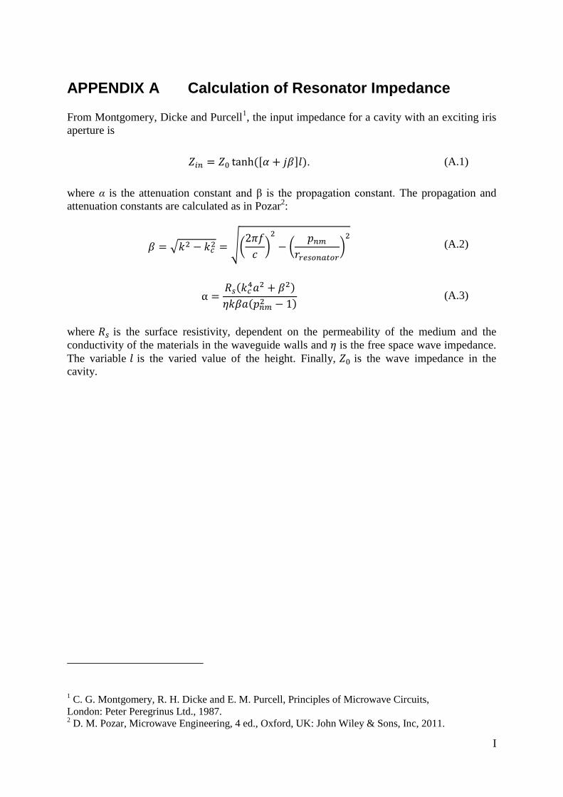
I
Calculation of Resonator Impedance APPENDIX A
From Montgomery, Dicke and Purcell1, the input impedance for a cavity with an exciting iris
aperture is
𝑍𝑖𝑛 = 𝑍0 tanh([𝛼 + 𝑗𝛽]𝑙). (A.1)
where α is the attenuation constant and β is the propagation constant. The propagation and
attenuation constants are calculated as in Pozar2:
𝛽 = √𝑘2 − 𝑘𝑐2 = √(
2𝜋𝑓
𝑐)2
− (𝑝𝑛𝑚
𝑟𝑟𝑒𝑠𝑜𝑛𝑎𝑡𝑜𝑟)2
(A.2)
α =
𝑅𝑠(𝑘𝑐4𝑎2 + 𝛽2)
𝜂𝑘𝛽𝑎(𝑝𝑛𝑚2 − 1)
(A.3)
where 𝑅𝑠 is the surface resistivity, dependent on the permeability of the medium and the
conductivity of the materials in the waveguide walls and 𝜂 is the free space wave impedance.
The variable 𝑙 is the varied value of the height. Finally, 𝑍0 is the wave impedance in the
cavity.
1 C. G. Montgomery, R. H. Dicke and E. M. Purcell, Principles of Microwave Circuits,
London: Peter Peregrinus Ltd., 1987. 2 D. M. Pozar, Microwave Engineering, 4 ed., Oxford, UK: John Wiley & Sons, Inc, 2011.

II
Equivalent Circuit of Slits and Diaphragms APPENDIX B
in Waveguide-to-Cavity Ports
Montgomery, Dicke and Purcell3
describe how thin metal sheets can be inserted in
waveguides to introduce a shunt reactive element 𝑗𝐵, when the thin metal sheets form a slit
through which electromagnetic field can propagate. The orientation of the slit opening
determines if the reactive element is inductive or capacitive; a slit parallel with the electrical
field will give rise to a shunt inductance, a slit perpendicular to the electrical field will give
rise to a capacitive impedance3.
Slit parallel with the electrical field:
𝐵 = −𝜆𝑔
𝑎cot2
𝜋𝑑
2𝑎+ 𝑓 (
𝑎
𝜆).
Slit orthogonal to the electrical field:
𝐵 = −4𝑏
𝜆𝑔ln (csc
𝜋𝑑
2𝑎).
3 C. G. Montgomery, R. H. Dicke and E. M. Purcell, Principles of Microwave Circuits,
London: Peter Peregrinus Ltd., 1987.
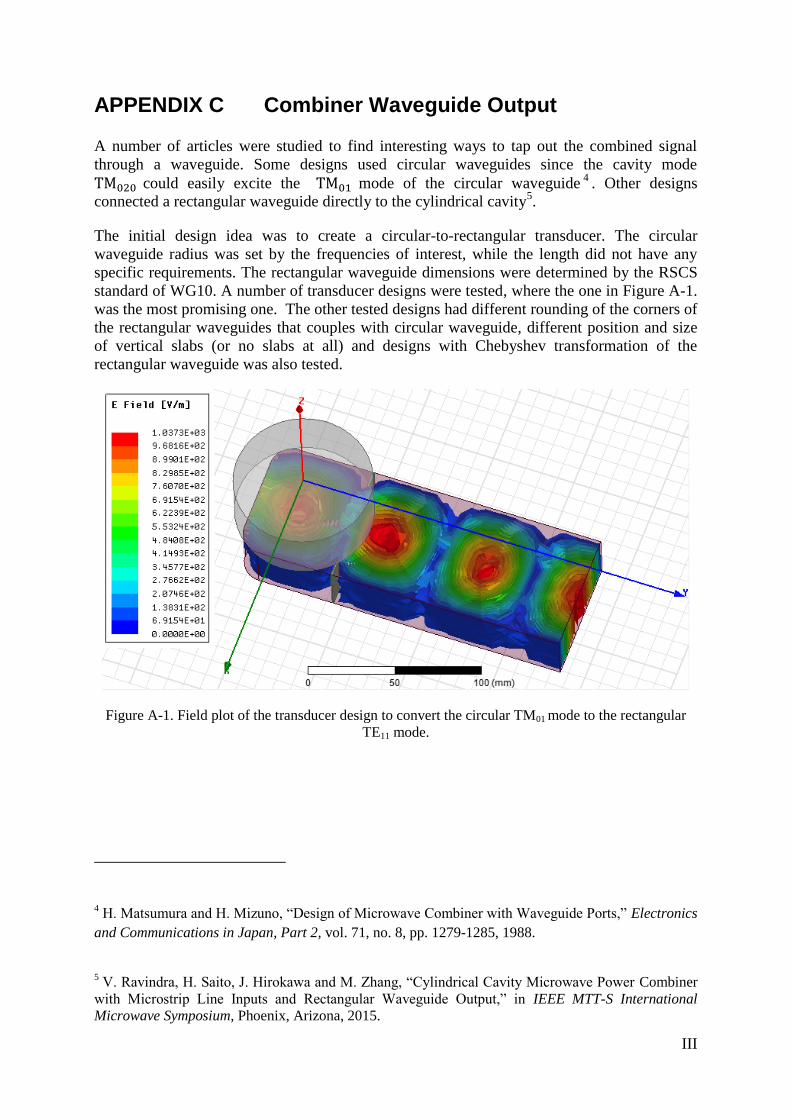
III
Combiner Waveguide Output APPENDIX C
A number of articles were studied to find interesting ways to tap out the combined signal
through a waveguide. Some designs used circular waveguides since the cavity mode
TM020 could easily excite the TM01 mode of the circular waveguide4
. Other designs
connected a rectangular waveguide directly to the cylindrical cavity5.
The initial design idea was to create a circular-to-rectangular transducer. The circular
waveguide radius was set by the frequencies of interest, while the length did not have any
specific requirements. The rectangular waveguide dimensions were determined by the RSCS
standard of WG10. A number of transducer designs were tested, where the one in Figure A-1.
was the most promising one. The other tested designs had different rounding of the corners of
the rectangular waveguides that couples with circular waveguide, different position and size
of vertical slabs (or no slabs at all) and designs with Chebyshev transformation of the
rectangular waveguide was also tested.
Figure A-1. Field plot of the transducer design to convert the circular TM01 mode to the rectangular
TE11 mode.
4 H. Matsumura and H. Mizuno, “Design of Microwave Combiner with Waveguide Ports,” Electronics
and Communications in Japan, Part 2, vol. 71, no. 8, pp. 1279-1285, 1988.
5 V. Ravindra, H. Saito, J. Hirokawa and M. Zhang, “Cylindrical Cavity Microwave Power Combiner
with Microstrip Line Inputs and Rectangular Waveguide Output,” in IEEE MTT-S International
Microwave Symposium, Phoenix, Arizona, 2015.

IV
Figure A 2. Plotted input reflection coefficient at circular waveguide: dB(S(1:3),S(1:3)), output
reflection coefficient at rectangular waveguide: dB(S(N:1),S(N:1)) and transmission
dB(S(1:3),S(N:1)). The reflection coefficient is less than 9 dB for the input reflection coefficient and
less than 16 dB for the output reflection coefficient for the range of 2.9 GHz to 3.3 GHz. The
transmission losses are lower than 1.5 dB over the same range.
Figure A 3. Smith chart presentation of input reflection coefficient at circular waveguide:
dB(S(1:3),S(1:3)), output reflection coefficient at rectangular waveguide: dB(S(N:1),S(N:1)) and
transmission dB(S(1:3),S(N:1)).
An alternative solution is to use probe excitation of the rectangular waveguide, which can be
realized in a number of ways6. This alternative was not considered within the scopes of this
project but could be of interest to study in further work.
6 F. K. Gharekand, “Design of a 16 Way Radial Microwave Power Divider/Combiner with Rectangular
Waveguide Output and Coaxial Inputs,” International Journal of Electronics and Communications, vol. 68, no.
5, pp. 422-428, 2014.

I