analysis and experimentation of modular differential
TRANSCRIPT
IEEJ Journal of Industry ApplicationsVol.9 No.5 pp.573–583 DOI: 10.1541/ieejjia.9.573
Paper
Analysis and Experimentation of Modular Differential Inverter UtilizingSEPIC Modules and SIC Devices for Grid Connected Applications
Ahmed Shawky∗,∗∗a)Student Member, Mahmoud A. Sayed∗∗∗ Non-member
Takaharu Takeshita∗ Fellow
(Manuscript received Oct. 16, 2019, revised Feb. 26, 2020)
This paper presents a three-phase Modular Differential Inverter (MDI) utilizing DC-DC modules that provide ACpower to the utility grid with step-up voltage capability. The construction of the MDI has many advantages such asflexibility and reliability, and can be designed, optimized and scaled to any power level. Moreover, Single–EndedPrimary–Inductor Converter (SEPIC) modules have been proposed to incorporate in the MDI because it has manymerits that enhance the overall performance of the differential inverter. SiC devices are also integrated into the SEPICmodules for efficient operation at a high switching frequency. An in-depth mathematical model discussing the practicalissues of differential inverter such as variable duty cycle, low order harmonics and circulating power is also presented.The design steps of the proposed SEPIC modules are presented in detail considering the standard grid side requirementsof total harmonic distortion (THD). The MDI, which implements three parallel modules in each phase, is investigatedusing PSIM simulation software. A mismatch of ±20% in the SEPIC module parameters of each phase is investigatedto confirm the system performance. Moreover, a laboratory prototype of the system, considering only one SEPICmodule in each phase with 200 V grid-side voltage, 1.6 kW, and 50 kHz switching frequency, is carried out to verifythe validity of the system.
Keywords: modular inverter, differential topology, SEPIC modules
1. Introduction
The recent increase in DC sources, such as renewable en-ergy, has accelerated the development of inverters for grid-connecting applications (1) (2). Three-phase inverter topolo-gies can process more power, compared to the single-phaseinverter topologies (3) they mitigate the power pulsation atdouble-line frequency and enhance reliability (4). Unlike two-stage and multi-stage inverter topologies, Single-Stage BoostInverter (SSB-I) topologies have been widely investigated forprocessing power through a single stage. These topologiesshould perform galvanic isolation in addition to voltage gain,in order to reduce the common-mode voltage (CMV) andleakage current.
The growing interest in this direction has returned atten-tion to differential based inverters (5)–(17). There has been in-creased use of these topologies in grid-connected applica-tions, despite their voltage and current stress. Differentialbased inverter topologies have a simple construction, based
a) Correspondence to: Ahmed Shawky. E-mail: [email protected]∗ Department of Electrical and Mechanical Engineering, Nagoya
Institute of TechnologyNagoya, Japan
∗∗ Electrical Engineering Department Aswan Faculty of Engineer-ing, Aswan UniversityEgypt
∗∗∗ Department of Electrical Power and Machines Engineering,Faculty of Engineering, South Valley UniversityQena, Egypt
on DC-DC converters. This construction provides voltagegain and voltage isolation by using isolated voltage step-up converters. These converters use High-Frequency Trans-formers (HFT) to enhance the size and weight of differentialinverter. The symmetrical operation of these converters fa-cilitates scaling up for use at greater power. This is achievedby using more parallel converters and maintaining a modularconstruction. Finally, Differential based inverters can be con-trolled using simple controllers which closely resemble thecontrol of traditional Voltage Source Inverters (VSI).
The THD of differential inverters is a major issue due tolow order harmonics and DC offset. Low order harmon-ics can be divided into two different components a negativesequence second-order harmonic component (NSHC), andother low order components higher than NSHC (i.e. 3rd, 4rd,and 5rd). both components are solved individually. In (5)–(8), an additional control loop has been discussed and im-plemented to mitigate NSHC. the other low order harmoniccomponents have been eliminated using static linearizationtechniques. To mitigate DC offset, an additional control loopwas proposed in (8). Moreover, to reduce THD less than 5%,additional control loops were proposed to mitigate other is-sues, such as PWM modulation and dead time effect (8).
Extensive work on differential inverter topologies has beenpublished. A three-phase transformer-less differential basedinverter is presented in (5). This inverter uses buck-boost con-verters, such as D1, D2, flyback, SEPIC and Cuk converters.Three-phase and single-phase Cuk Differential based inverterhave been implemented in (6), (7) and (8). Single-phase and
c© 2020 The Institute of Electrical Engineers of Japan. 573

Analysis and Experimentation of Modular Differential Inverter(Ahmed Shawky et al.)
three-phase boost differential based inverter were proposedat (9)– (11) and (12)– (14) respectively. All previous topolo-gies are modulated using three different modulation schemes.First, the Continuous Modulation Scheme (CMS) allows ACpower to be properly fed with a stable performance, whichis beneficial for grid-connected applications (5) (6). Second,the Discontinuous Modulation Scheme (DMS), presented in(7), (8), reduces circulating power loss in addition to volt-age and current stress. In addition to CMS and DMS, thethird-order harmonic injection modulation scheme was pro-posed for the three-phase boost differential inverter in (14).This modulation scheme shows significant improvements tovoltage and current stress. Although DMS and third-orderharmonic injection modulations decrease second-order har-monics, they produce additional low order harmonics thatare higher than NSHC, thereby more additional control loopsare required. Most aforementioned topologies are controlledwith linear controllers, such as proportional resonance (PR).On the other hand, nonlinear control methods, such as thesliding mode control method, are implemented in the differ-ential inverters in (9), (12). In (13), a control technique for agrid-connected boost differential based inverter was proposedto enhance power quality. This technique uses three controlloops, including feedforward linearized current control andbidirectional power control for battery operation.
Although previous literature has improved the performanceof differential based inverter topologies, the following pointsare common to all
1. There is no focus on the modular construction of dif-ferential based inverter and its mismatch effect.
2. Detailed design of DC-DC modules is not well cov-ered.
3. The differential inverter characteristics (variable dutycycle, low order harmonics and circulating power) arenot discussed during the design of DC-DC modules.
Motivated by this, the design and control technique of theSEPIC differential based inverter and its modular techniqueMDI for high power application is presented in this paper.The operation of the MDI has been described mathemati-cally considering parallel SEPIC modules in each phase. Thedesign steps of the proposed SEPIC module have been con-ducted based on the derived mathematical model. Further-more, this model investigates the influence of the differentialinverter characteristics on the DC-DC SEPIC modules. Fi-nally, a design example based on a three-phase MDI is car-ried out in PSIM simulation software, considering a ±20%mismatch between the parallel modules of each phase, in or-der to investigate system performance in the case of unsym-metrical modules. Moreover, the system performance and itscontrol technique have been investigated experimentally con-sidering only one SEPIC module per phase, using a 200 V,1.6 kW laboratory prototype.
2. Steady State Analysis of Modular DifferentialInverter MDI
Generally, a grid-connected MDI is composed of n DC-DCmodules per phase, as illustrated in Fig. 1. These modules areconnected in an Input-Parallel Output-Parallel (IPOP) config-uration. For a three-phase grid, the output terminals of thesephases are connected differentially. More modules (n > 1)
Fig. 1. Main Circuit of Three-phase MDI
Fig. 2. General waveform of DC-DC modules operatingat MDI
are required when the processing power at each phase islarger than the rated power of the utilized modules. In otherwords, the MDI processes high power using 3 ∗ n small DC-DC modules.2.1 Basic Operation Fundamental operation of a
MDI depends on driving DC-DC modules with a variableduty cycle. this duty cycle produces an AC output voltagewith a common DC offset as shown in Fig. 2. It is worthnoting that this offset will appear at the common point, C,as shown in Fig. 1. Unlike conventional DC-AC circuits,this DC offset comes from the unipolar operation of DC-DCmodules and was cancelled out by the three-phase differen-tial connection at the grid side. The derived DC-DC modulesof the same phase have a 0◦ phase shift, whereas the DC-DCmodules of different phases have a 120◦ phase shift.2.2 Mathematical Model According to Fig. 1, the
phase voltages and phase currents of a balanced three-phasegrid can be given as follows:
574 IEEJ Journal IA, Vol.9, No.5, 2020
Analysis and Experimentation of Modular Differential Inverter(Ahmed Shawky et al.)
⎡⎢⎢⎢⎢⎢⎢⎢⎣esu(t)esv(t)esw(t)
⎤⎥⎥⎥⎥⎥⎥⎥⎦ = Emax
⎡⎢⎢⎢⎢⎢⎢⎢⎢⎢⎢⎢⎢⎢⎢⎢⎢⎢⎢⎢⎣
sin (ωt)
sin
(ωt − 2π
3
)
sin
(ωt +
2π3
)⎤⎥⎥⎥⎥⎥⎥⎥⎥⎥⎥⎥⎥⎥⎥⎥⎥⎥⎥⎥⎦
⎡⎢⎢⎢⎢⎢⎢⎢⎣isu(t)isv(t)isw(t)
⎤⎥⎥⎥⎥⎥⎥⎥⎦ = Imax
⎡⎢⎢⎢⎢⎢⎢⎢⎢⎢⎢⎢⎢⎢⎢⎢⎢⎢⎢⎢⎣
sin (ωt)
sin
(ωt − 2π
3
)
sin
(ωt +
2π3
)⎤⎥⎥⎥⎥⎥⎥⎥⎥⎥⎥⎥⎥⎥⎥⎥⎥⎥⎥⎥⎦· · · · · · · · · · · · · · · · · · · (1)
where Emax presents the maximum phase voltage, Imax
presents the maximum phase current, and ω indicates theline frequency. The simplest version of a MDI has one DC-DC module per phase for processing the power. The powerof each module changes instantaneously with line frequency.However, all phases process the same average power, and allmodules have the same peak and valley power, and work in asymmetrical operation. The only difference comes from theintroduced phase shift of 120◦.
To obtain a voltage step-up, any bidirectional boost orbuck-boost DC-DC module can be utilized. The voltage andcurrent gain of a boost converter is expressed as follows:
vmx
VDC=
imx
iomx=
11 − dx
· · · · · · · · · · · · · · · · · · · · · · · · · · · (2)
The voltage gain and current gain of the buck-boost con-verter is
vmx
VDC=
imx
iomx=
dx
1 − dx· · · · · · · · · · · · · · · · · · · · · · · · · · · (3)
As shown in Figs. 1 and 2, vmx represents the instantaneousoutput voltage of the associated DC-DC module, x, in Phasem. Here, x indicates the number of DC-DC modules in eachphase (x = 1, 2, 3, . . . .n), while m indicates the associatedphase (m = u, v, and w). For example, vu1 is the instanta-neous output voltage of the first DC-DC module at phase u.The same scenario can be applied for input and output cur-rents, e.g., iu1, iou1 represent the input and output currents ofthe first DC-DC module at phase u, respectively. VDC repre-sents the input DC voltage and dx represents the duty cycleof this module.
For MDI, the total input current of one phase can be ex-pressed as follows:
iinm =
n∑x=1
imx · · · · · · · · · · · · · · · · · · · · · · · · · · · · · · · · · · · · (4)
For all phases, the total input current can be expressed asfollows:
IDC = iinu + iinv + iinw · · · · · · · · · · · · · · · · · · · · · · · · · · · · (5)
On the other hand, the output voltages of the modules ofone phase are equal and can be expressed as follows:
vm1 = vm2 = . . . vmn = vmx · · · · · · · · · · · · · · · · · · · · · · · · (6)
For all phases, RMS value of the output voltages are equal.The phase current of grid can then be expressed as follows:
ism =
n∑x=1
iomx · · · · · · · · · · · · · · · · · · · · · · · · · · · · · · · · · · · (7)
Many modulation strategies were presented for the controlof differential based inverters. It worth noticing that a simplemodulation strategy, without additional feedforward sensingand complicated calculations, is required for a MDI. There-fore, the modulation employed in (15) is used in this work asit provides static linearization and suits modularity. More-over, it can be applied to boost and buck-boost DC-DC mod-ules. From (3), the duty the duty cycle can be expressed asfollows:
dx =vmx
vmx + VDC· · · · · · · · · · · · · · · · · · · · · · · · · · · · · · · · · (8)
As presented in Fig. 2, the differential inverter producestwo voltage components at the output of the DC-DC mod-ule: the DC common voltage VDo and an AC voltage. Forideal operation, it is worth noticing that this common volt-age is equal at all modules, despite the connected phase. Theoutput voltage of the utilized module can then be simplifiedto
vmx(t) = VDo + esm(t) · · · · · · · · · · · · · · · · · · · · · · · · · · · · (9)
where esm(t) is the associated phase voltage connected to themodule (see Eq. (1)). Since both components come from thesame module, they have the same voltage gain. The outputvoltage from (9) can then be expressed as follows:
vmx(t) = MVDC + MVDC K = MVDC(1 + K) · · · · · · (10)
where M is the actual static gain of the differential inverter.Term K is the sinusoidal differential constant of the outputvoltage that introduce the behavior of grid and can then beexpressed as follows:
K =
⎡⎢⎢⎢⎢⎢⎢⎢⎢⎢⎢⎢⎢⎢⎢⎢⎢⎢⎢⎢⎣
sin (ωt)
sin
(ωt − 2π
3
)
sin
(ωt +
2π3
)⎤⎥⎥⎥⎥⎥⎥⎥⎥⎥⎥⎥⎥⎥⎥⎥⎥⎥⎥⎥⎦· · · · · · · · · · · · · · · · · · · · · · · · · · · · (11)
By comparing (2), (3), (9) and (10), the actual static volt-age gain of MDI can be outlined as follows:
M = 0.5vmx(max)
VDC· · · · · · · · · · · · · · · · · · · · · · · · · · · · · ·(12)
The maximum value of vmx is defined at K = 1. From (12),MDI gain, M, is equal to half of the maximum voltage gainof the utilized DC-DC module, e.g., if the maximum voltagegain of the utilized DC-DC module is 4, then the actual staticgain M is 2. Practically, the voltage gain is reduced by thevoltage drop of the parasitic components of the DC-DC mod-ules. Therefore, it is imperative to use DC-DC modules withsmall parasitic components.
By substituting equations (10), (11) into (8), the duty cycleof the utilized DC-DC module can be given as
dx(t) =M(1 + K)
M(1 + K) + 1· · · · · · · · · · · · · · · · · · · · · · · · · · (13)
From (13), the duty cycle of the associated DC-DC module
575 IEEJ Journal IA, Vol.9, No.5, 2020
Analysis and Experimentation of Modular Differential Inverter(Ahmed Shawky et al.)
x depends on two different variables the gain of the MDI, M,and the associated connected phase, K. Thus, this modula-tion supports the modularity of the MDI and each of the uti-lized DC-DC modules will work independently. Moreover,the control structure does not require major changing if usingthe MDI at a greater power.
Since the boost DC-DC modules working at MDI, theirinput current, according to (2) and (13), can be derived asfollows:
imx(t) = 0.5Miomx(t) + iomx(t)(M + 1)K − 0.5Miomx(t)K2
· · · · · · · · · · · · · · · · · · · (14)
According to (3) and (13), the input current of buck-boostDC-DC modules working at MDI is outlined as
imx(t) = 0.5Miomx(t) + iomx(t)MK − 0.5Miomx(t)K2
· · · · · · · · · · · · · · · · · · · (15)
In both, term, K2 represents the sinusoidal differential con-stant of input current for associated DC-DC modules and canbe expressed as follows:
K2 =
⎡⎢⎢⎢⎢⎢⎢⎢⎢⎢⎢⎢⎢⎢⎢⎢⎢⎢⎢⎢⎢⎢⎣
cos [2 (ωt)]
cos
[2
(ωt − 2π
3
)]
cos
[2
(ωt +
2π3
)]
⎤⎥⎥⎥⎥⎥⎥⎥⎥⎥⎥⎥⎥⎥⎥⎥⎥⎥⎥⎥⎥⎥⎦· · · · · · · · · · · · · · · · · · · · · · · (16)
The term, K2, accurately describes the circulating power be-tween different phases at the differential inverter. This circu-lating power is evaluated at the double frequency because areverse power circulates instantaneously from the other twophases in each cycle of grid frequency, as shown in Fig. 2 (15).This constant should be considered during the design processof DC-DC modules in order to achieve proper operation ofthe MDI. Based on (14), the input power of the boost DC-DCmodules used at the MDI can be expressed as follows:
pinmx(t) = 0.5MVDCiomx(t) + VDCiomx(t)(M + 1)K
− 0.5MVDCiomx(t)K2 · · · · · · · · · · · · · · · · (17)
Using the same process for buck-boost based DC-DC mod-ules, according to (15), the input power can be expressed asfollows:
pinmx(t) = 0.5MVDCiomx(t) + VDCiomx(t)MK
− 0.5MVDCiomx(t)K2 · · · · · · · · · · · · · · · · (18)
3. Proposed SEPIC Module
Since the MDI converts power between a DC source andthe grid, its parallel DC-DC modules should maintain the ob-jectives presented in Fig. 3. DC-DC modules having a two-switch structure are preferred for achieving low componentcounts and a high efficiency and can work within the duty cy-cle range of 0.0 < dx < 0.9. From (2), (3), and (12), Fig. 4shows the voltage gain and possible maximum static gain,M, of the MDI, utilizing boost and buck-boost modules, re-spectively. It worth mentioning that both of them have anapproximate static gain.
In perspective of voltage and current stress, according (10)
Fig. 3. System Requirements of grid-connected MDI
Fig. 4. Voltage gain of boost and buck-boost Modulesand MDI static gain at duty cycle range
Table 1. Circuit parameters of MDI
and (13), and assuming the parameters in the Table 1, Fig. 5illustrates the duty cycle, output voltage, switches’ voltageand current stress of boost and buck-boost modules. Here,the static gain M and equivalent output resistance Rmx areassumed 2.0 and 100Ω, respectively. S 1, S 2 are the comple-mentary switches of these modules (16). Notice that the voltagestress is equal for both types. However, the current stress ofboth switches is lower in buck-boost modules.
The continuous input current is an important factor for re-newable energy DC sources, such as PVs and Fuel cells. Thiswill add two important features. Firstly, the input inductor ofthese modules prevents issues related to the short circuit cur-rent. Secondly, it eliminates the large electrolyte input capac-itor integrated between the DC source and the MDI, requiredto decrease the switching ripples (4) (5) (16). From this point ofview, boost converters and other buck-boost converters, suchas SEPIC and Cuk converters, are preferred due to their con-tinuous input current. From (14) and (15), input current stresson the DC source for both modules is illustrated in Fig. 6 atiomx = 8 A. Obviously, buck-boost converters have a lowerinput current stress.
According to the grid, voltage isolation is important forCMV and EMI. This issue can be implemented by usingHFT based DC-DC converters such as SEPIC, Cuk, and fly-back. Moreover, HFT based topologies are better for low DC
576 IEEJ Journal IA, Vol.9, No.5, 2020

Analysis and Experimentation of Modular Differential Inverter(Ahmed Shawky et al.)
Fig. 5. Duty cycle, output voltage, voltage and currentstress of boost and buck-boost DC-DC Modules at onecycle of grid frequency
Fig. 6. Input current of boost and buck-boost Modulesat differential inverter on one cycle of grid frequency
current injection. Finally, the THD of the grid current shouldbe within acceptable limits, which depends on the MDI con-trol rather than the utilized DC-DC modules.
Based on the previous discussion, SEPIC and Cuk convert-ers are preferred. However, the SEPIC converter is proposedin this work due to its low component count and the low en-ergy storage of its components (5) (15) (17).
4. Design Steps of Proposed SEPIC Module
The design process of the proposed SEPIC module isshown in Fig. 7. In the case of more than one module perphase, the process should be repeated in the following pat-tern n = 1, 2, . . .. The boundary conditions are defined by thefollowing points:
✔ (Maximum n) is limited by the efficiency of the SEPICmodule. Efficiency is generally low at low ratedpower due to high power losses in particular, switch-ing losses (16) (18) (19). The DC-DC modules in the 100 Vrange are most efficient when operated at several hun-dred watts (300 W ≤ Power ≤ 700 W). Similar con-verters are implemented in modular systems such asdata centers, UPSs, and smart grids (20)–(24).
Fig. 7. Flowchart of the design steps for the proposedSEPIC module utilized in MDI
✔ (Minimum n ≥ 1), is limited by the current rating ofthe SEPIC module. The voltage gain of the DC-DCmodule is inversely proportional to the rated current.At high current, the voltage drop will increase and willnot provide a sufficient voltage gain for MDI (16) (18).
4.1 Specifications of MDI The circuit parameters ofthe presented MDI are shown in Table 1. The power of, oneSEPIC module, per phase can be expressed as follows:
Pmodule =PMDI
3 ∗ n=
16003 ∗ 1
= 533.3 w · · · · · · · · · · · · · (19)
Form grid specifications, the phase voltage and phase cur-rent of each module are Emax = 163.29 v and Imax = 6.532 A,respectively. From (9, 12), the static gain of MDI can be ob-tained as follows:
M =163.29 + 163.29
2 ∗ 100= 1.63 · · · · · · · · · · · · · · · · · · · (20)
The voltage gain of SEPIC Module should be larger than2 ∗ M as shown in Fig. 2. Therefore, the design is conductedbased on gain M = 4 to consider the voltage drop of parasiticcomponents. In SEPIC modules, the acceptable percentageof capacitor voltage ripple and inductor current ripple are lessthan 10% and 20%, respectively (16). To achieve these ripplepercentages, a 50 kHz switching frequency is used to controleach SEPIC module.4.2 Components Selection of Proposed SEPIC Mod-
ule Figure 8 shows the schematic of the proposed SEPICmodule. The module implemented two power switches (amain switch, S m, and a synchronous switch, S r), two capac-itors (a coupling capacitor, Cx, and output capacitor, Cox), aninput inductor Lx, and a single-phase HFT. Based on Fig. 2,this module processes the power in two directions. Forwardpower is implemented using S m and the body diode of S r.For reverse power, the body diodes of S m and S r are used.Converter parasitic resistances, such as the DC resistance ofthe input inductor, rx, and the primary and secondary resis-tances, Rpri and Rsec, of the HFT have been considered in
577 IEEJ Journal IA, Vol.9, No.5, 2020

Analysis and Experimentation of Modular Differential Inverter(Ahmed Shawky et al.)
Fig. 8. Schematic of Proposed SPIC module utilized inMDI
order to obtain an accurate design. Due to symmetry in thepower operation, only the forward power is analyzed in thispaper. Complementary switching of S m and the body diodeof S r produce the output voltage:
Vmx
VDC=
dx
1 − dx∗ Rmx
Rmx +dx ∗ KP
1 − dx(Rmx + KR)
KP = rx +Rpri[dx ∗ (1 − dx) + (1 − dx)2]
dx
KR =Rm[d2
x + (1 − dx)2]dx ∗ (1 − dx)
+Rsec + RD
dx· · · · · · · · · · (21)
where Rm, RD represent the on-resistances of main and syn-chronous switches, respectively. Rmx is the equivalent outputresistance of grid phase connected to this module, which is25Ω.
The maximum voltage stress, Vs and current stress, Is ofboth switches are equal in SEPIC converter and are given as:
Vs = VDC + Vmx = 100 + 4 ∗ 100 = 500 v
Is = ILx + IT x =
[dx
1 − dx+ 1
]Imax = 32.66 A · · · · (22)
where Ilx, Ilmx represent the average current of the input in-ductor and the HFT’s magnetizing inductance, respectively.Considering the voltage and current ripples, the maximumswitch current and maximum voltage will be 35 A and 600 V.Therefore, SiC devices with a part number C2M0040120Dare selected for both switches in the proposed SEPIC module.SiC devices are preferred because they have low conductionand switching losses, which implies a high efficiency. More-over, they have a high blocking voltage and current capabil-ity in order to withstand the voltage and current stress of theMDI (25) (26).
From (13) and Fig. 5, the variable duty cycle introducesvariable input and output current ripples at the proposedSEPIC. The inductors and capacitors should be designed forthe highest introduced ripple. This will happen at a high dutycycle (dx = 0.8). The inductors and capacitors can be formu-lated as follows:
Lx =dx ∗ VDC
2 ∗ Δilx ∗ Fsw=
0.8 ∗ 1002 ∗ 26.128 ∗ 0.20 ∗ 50000
= 153 μH
Lmx =dx ∗ VDc
2 ∗ Δilmx ∗ Fsw=
0.8 ∗ 1002 ∗ 6.532 ∗ 0.25 ∗ 50000
= 489.89 μH
Fig. 9. PCB implementation of Proposed SEPIC mod-ule utilized in MDI
Cx =d2
x
1 − dx∗ VDc
2 ∗ Rmx ∗ ΔVcx ∗ Fsw
=2.25 ∗ 100
2 ∗ 25 ∗ 100 ∗ 0.1 ∗ 50000= 12.8 μF
Cox =
(dx
1 − dx
)2
∗ Vdc
2 ∗ Rmx ∗ ΔVcox ∗ Fsw
=4∗4∗100
2∗25∗500∗0.1∗50000=12.72 μF · · · · · · · (23)
According (23), The input and magnetizing inductance areselected as 180 μH and 490 μH, respectively. Furthermore,14 μF is selected for both the coupling and output capaci-tance.
Figure 9 illustrates the PCP board of the proposed SEPICmodule, based on previously designated values. Film capac-itors were used for the coupling capacitor, output capacitor,and the clamp capacitor to increase its reliability. A clampcapacitor was introduced as part of the clamp circuit in or-der to suppress high voltage spikes generated from the leak-age inductance of the HFT. Furthermore, heat sink was intro-duced for stable heat dissipation. Finally, gate-drive of theSiC switches was implemented on the same board to supportthe modularity of the MDI.4.3 Design Steps of Passive Magnetic ElementsOutstanding materials suitable for the HFT and input induc-
tor are monocrystalline, amorphous, and ferrites. For the pro-posed SEPIC module, a soft ferrite core (EER-94) is used, forboth to achieve low loss and cost (27) (28). The permeability ofthis core is μr = 2500. Ae = 712 mm2 and Ve = 158000 mm3
are the effective area and effective volume, respectively. Themaximum flux density is Bmax = 470 T. In order to decreaseeddy currents and hysteresis losses, LITZ wire has been usedfor their windings.
For many years, the basic magnetic theory of the traditionalline frequency transformers was used to design HFTs. Theturns of HFT can be expressed using equation (24). Thisequation assumed that the primary and secondary windingsof a HFT behave like inductors (16) (27) (29) and the magnetic ma-terial is composed of one heterogeneous structure. Moreover,it designs HFTs as an independent block by considering onlythe magnetic elements of a HFT, such as the core geometryand number of turns.
578 IEEJ Journal IA, Vol.9, No.5, 2020

Analysis and Experimentation of Modular Differential Inverter(Ahmed Shawky et al.)
Fig. 10. Implemented HFT of proposed SEPIC module
Fig. 11. Implemented input inductor of proposed SEPICmodule
N =
√Lmx ∗ Ve
μo ∗ μr ∗ Ae· · · · · · · · · · · · · · · · · · · · · · · · · · · · (24)
Recently, most isolated DC-DC converters have compli-cated magnetic structures, composed of multiple windingsand multiple heterogeneous elements (cores and air gaps).These converters require air gaps to store energy during thecomplementary switching operation (30). For MDI, the pro-posed SEPIC module has a variable terminal voltage at theHFT due to its variable duty cycle. Therefore, the number ofturns can be obtained as follows:
N =Von ∗ (1 − D) ∗ Ts
ΔB ∗ Ae· · · · · · · · · · · · · · · · · · · · · · · · · (25)
Equation (25) considers the circuit parameters of theSEPIC module as well as the core geometry. The circuit pa-rameters is introduced by the maximum volt-second, Von, onthe primary turns of the HFT when the main switch, S m, isoff. From (25), the number of turns is 9. To mitigate the re-duction in magnetizing inductance coming from existed airgap, 15 turns is used in the HFT design.
On the other hand, the number of turns for input inductorscan be expressed as follows:
N =Lx ∗ Ipk
Ae ∗ ΔB· · · · · · · · · · · · · · · · · · · · · · · · · · · · · · · · · · (26)
Ipk is the maximum current of the inductor before saturation.Ipk = 30 A is selected for maximum saturation current. From(26), the turns number for input inductor is 32. Practically,for higher saturation current, the turns number is increased to37 in the proposed SEPIC module. The implemented HFTand input inductor of the proposed SEPIC module are shownin Figs. 10 and 11, respectively. The magnetizing and leakageinductances of the HFT are 493.18 and 3.11 μH, respectively.The inductance of input inductor is 181.98 μH.
Fig. 12. Proposed Control of MDI
5. Proposed Control Technique
As shown in Fig. 12, a simple controller utilizing the d-qsynchronous reference frame is carried out for MDI. In thiscontrol, Loop 1 regulates the grid current to follow the refer-ence one. To obtain low THD, loop 2 is added to compensatethe NSHC, introduced by circulating power among modulesof different phases.
Like any modular architecture, SEPIC modules utilized inMDIs are not practically identical due to their componenttolerances, even in the case of having similar duty cycles.Component tolerances of the parasitic resistance at switches,passive elements, and PCBs shown in (21) are the varioussources of this mismatch. For the proposed SEPIC modules,there are two different cases of mismatch, Case I and Case II.
Case I considers the mismatch between SEPIC modules inthe same phase (i.e. phase u). The mismatch of componenttolerance is the only source. Case II considers the mismatchbetween SEPIC modules at different phases (i.e. phase u andv as shown in Fig. 1). The mismatch results from componenttolerance and the 120◦ phase shift.
In Case II, the SEPIC module with the lower parasitic re-sistance will instantaneously provide more power comparedwith the other module. Additionally, the 120◦ phase shift be-tween phases introduces a small voltage difference. Both ofthem will introduce a DC offset between the injected three-phase currents that circulate between phases. To solve this is-sue, a three stage low pass filter (LPF) is augmented in loop 2of the proposed control this mitigates the mismatch betweenSEPIC modules of different phases.
In Case I, thanks to the high sinking capability of the gridand the grid current control (loop 1), that fix the output volt-ages of each phase for the utilized parallel DC-DC modules.This self-balancing capability of the output voltages of eachphase is due to the identical duty cycle and input voltage thus,the mismatch appears in the current of the SEPIC modulesinstead of the voltage. Hence, there is no circulating cur-rent between different modules and no additional control isrequired (16).
6. Simulation Results
To verify the validity of the proposed control for the MDI,a circuit comprising of nine SEPIC modules is simulatedin PSIM software. System parameters of the MDI used inthe simulation are listed in Table 1. Three modules of the
579 IEEJ Journal IA, Vol.9, No.5, 2020
Analysis and Experimentation of Modular Differential Inverter(Ahmed Shawky et al.)
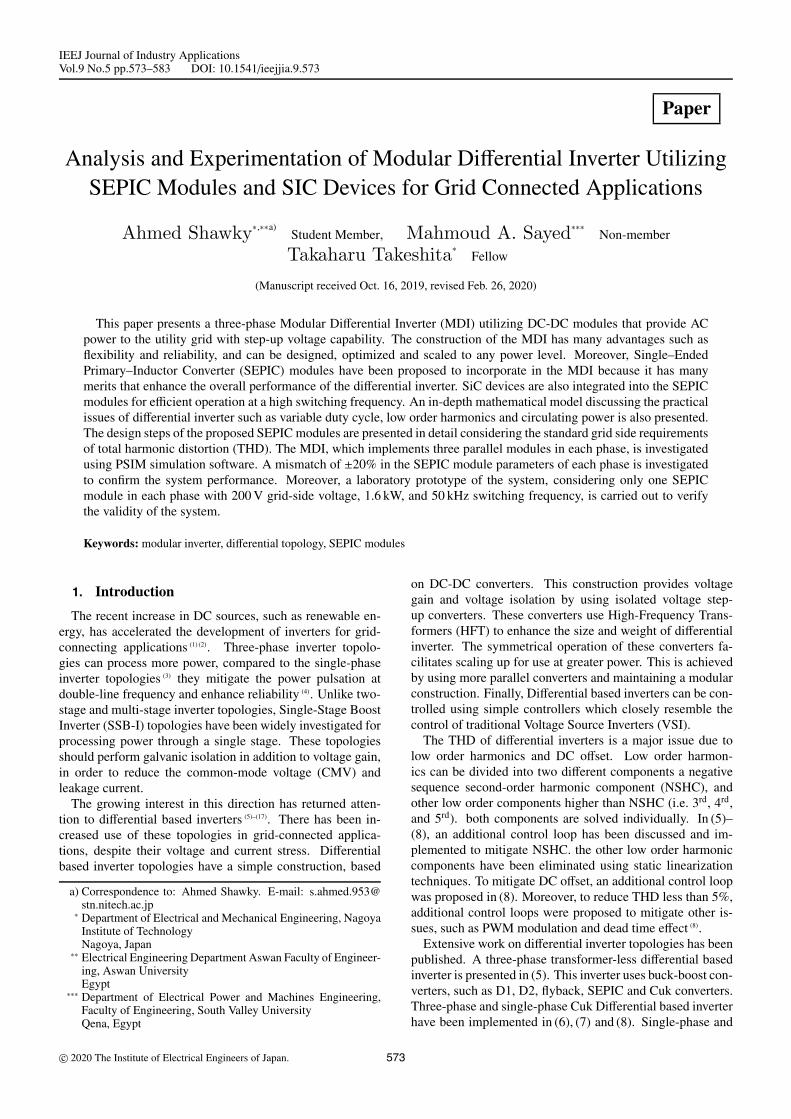
Fig. 13. Grid voltage, duty cycles, injected grid current,reference and actual current of MDI
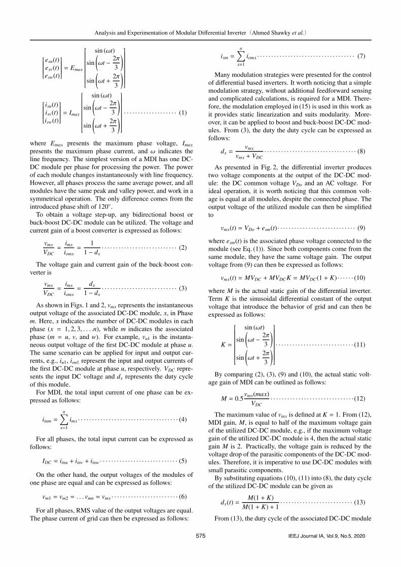
Fig. 14. Duty cycles, output voltages, input current ofSEPIC modules in phase u with ±20%
proposed S EPIC are connected in parallel in each phase inorder to process a triple high power, 4.8 kW. A mismatch incomponents is introduced to investigate the performance ofthe MDI.
A ±20% parameter mismatch is considered in the DC resis-tance of the input inductor for the first and third SEPIC mod-ules in phase u. Figure 13 illustrates the grid voltage, dutycycle (du, dv, dw), injected grid current (isu, isv, isw), referencecurrent, and actual current. The grid current is synchronizedwith grid voltage. The current is free from NSHC and the DCoffset, even at the existing mismatch between phase u and theother phases (phases v and w).
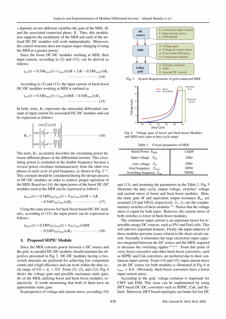
Figure 14 shows the duty cycles, output voltages and inputcurrents of the SEPIC modules connected at phase u. The ex-isted mismatch does not affect the output voltage due to thegrid voltage effect. The mismatch slightly affected input cur-rents as shown in Fig. 15. The maximum effect of mismatchresults at high duty cycle. The average input currents are26.4 A, 26.7 A and 27.0 A for Iu1, Iu2, Iu3 respectively. There-fore, the parameter mismatch of 20% resulted in a 0.3 A dif-ference of the input current.
Table 2 shows the maximum mismatch of the input currentand its percentage at (du = 0.8) due to ±20% disturbance inthe input inductance HFT magnetizing inductance, Couplingcapacitor, and output capacitors. In all cases, the three-phase
Fig. 15. Zoomed View of Fig. 14 at high duty cycle ofSEPIC modules connected in phase u
Table 2. The maximum mismatch current in PSIM atdifferent mismatch cases at du = 0.8
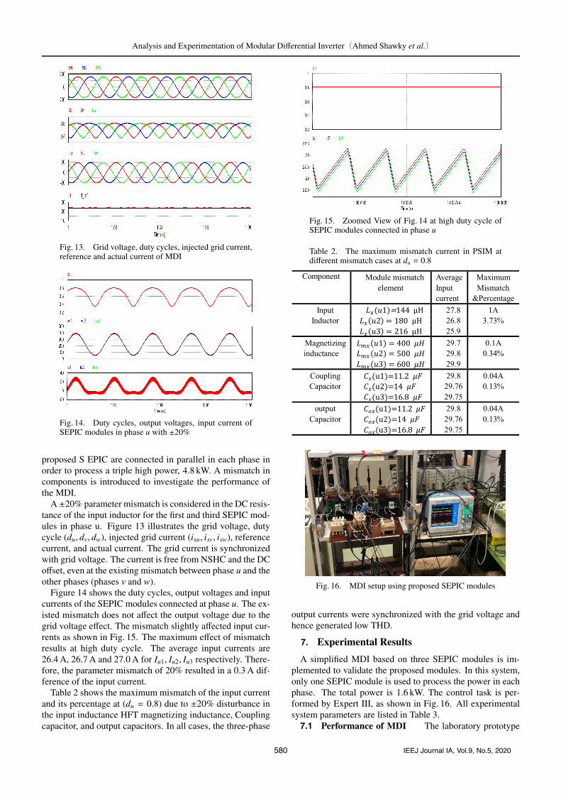
Fig. 16. MDI setup using proposed SEPIC modules
output currents were synchronized with the grid voltage andhence generated low THD.
7. Experimental Results
A simplified MDI based on three SEPIC modules is im-plemented to validate the proposed modules. In this system,only one SEPIC module is used to process the power in eachphase. The total power is 1.6 kW. The control task is per-formed by Expert III, as shown in Fig. 16. All experimentalsystem parameters are listed in Table 3.7.1 Performance of MDI The laboratory prototype
580 IEEJ Journal IA, Vol.9, No.5, 2020

Analysis and Experimentation of Modular Differential Inverter(Ahmed Shawky et al.)
Table 3. Final Components of Proposed SEPIC Module
Fig. 17. Phase voltages and Currents of three-phaseSEPIC MDI
Fig. 18. DC input voltage and Current of three-phaseSEPIC MDI
of the system is demonstrated at steady state operation witha 1.6 kW power flow, as shown in Figs. 16 and 17. Fig-ure 17 shows the phase voltages and phase currents. Fig-ure 18 shows the DC input voltage and current. Grid injectedcurrents are in-phase with the voltages. The grid currents aresinusoidal waveforms with low THD. It worth mentioningthat the NSHC is eliminated by the proposed control tech-nique. The FFT spectrum of the grid current is shown inFig. 19. Second order component is less than 2% of the spec-trum and have a THD of less than 6%. The DC offset causedby the module mismatch is less than 0.02 A.
Fig. 19. FFT of grid current of SEPIC based MDI
Fig. 20. Output voltages and input currents of utilizedSEPIC module
Fig. 21. Voltage and current stress of utilized SEPICmodule
7.2 Performance of SEPIC Modules Experimentalwaveforms of the output voltage of the SEPIC modules aredepicted in Fig. 20. The output voltage has two components(DC and AC), as discussed before, and coincide with Eq. (9)and Fig. 2.
The input inductor current of the proposed SEPIC indi-cates the power direction and coincides with Eq. (15) andFigs. 2 and 6. The maximum ripple of the input current is17.46% and 5% at the highest and lowest duty cycles, respec-tively. It is clear from Fig. 21 that the switches voltage andcurrent stress of the proposed SEPIC module are within thesave operating zone. Finally, the efficiency profile of the pro-posed SEPIC module at different power ratings is illustratedin Fig. 22.
581 IEEJ Journal IA, Vol.9, No.5, 2020

Analysis and Experimentation of Modular Differential Inverter(Ahmed Shawky et al.)
Fig. 22. Efficiency profile of proposed SEPIC module
8. Conclusion
This paper has proposed a SEPIC DC-DC module to be in-tegrated into the MDI. Furthermore, a detailed mathematicalmodel of the MDI has been presented. The design steps ofall passive elements of the SEPIC module have been illus-trated in detail. A detailed control scheme has been proposedto control each module of the system, considering compensa-tion for the second order harmonics NSHC due to the circu-lating power among the SEPIC modules. The performance ofthe MDI has been investigated using PSIM software, consid-ering three parallel modules in each phase. The effects of a±20% component mismatch in each module have been inves-tigated. Moreover, the system has been implemented experi-mentally, with only one module in each phase, to confirm thevalidity of the system and the effectiveness of the proposedcontrol technique. Experimental results clearly show that thecontrol technique regulates the power flow of the system tofollow the reference value and draws sinusoidal currents atthe grid having a unity power factor and low THD.
References
( 1 ) A. Shawky, A. Shier, M. Orabi, J. Abu Qahouq, and M. Youssef: “High Ef-ficiency Single-stage Current Source Inverter for Photovoltaic Applications”,in press, IEEE Telecomm. Energy Conf., INTELEC 2013, Hamburg, Ger-many (2013)
( 2 ) S. Harb, M. Kedia, H. Zhang, and R.S. Balog: “Micro inverter and stringinverter grid-connected photovoltaic system - A comprehensive study”, Proc.IEEE 39th Photovoltaic. Spec. Conf., pp.2885–2890 (2013)
( 3 ) M. Prodanovic and T.C. Green: “Control and filter design of three-phase in-verters for high power quality grid connection”, IEEE Trans. Power Electron.,Vol.18, No.1, pp.373–380 (2003)
( 4 ) H. Hu, S. Harb, N. Kutkut, I. Batarseh, and Z.J. Shen: “A Review of PowerDecoupling Techniques for Microinverters with Three Different DecouplingCapacitor Locations in PV Systems”, IEEE Trans. Power Electron., Vol.28,No.6, pp.2711–2726 (2013)
( 5 ) A. Darwish, A.M. Massoud, D. Holliday, S. Ahmed, and B.W. Williams:“Single-Stage Three-Phase Differential-Mode Buck-Boost Inverters withContinuous Input Current for PV Applications”, in IEEE Transactions onPower Electronics, Vol.31, No.12, pp.8218–8236 (2016)
( 6 ) A. Darwish, D. Holliday, S. Ahmed, A.M. Massoud, and B.W. Williams:“A single-stage three-phase inverter based on Cuk converters for PV appli-cations”, IEEE J. Emerging and Sel. Topics on Power Elec., Vol.2, No.4,pp.797–807 (2014)
( 7 ) S. Mehrnami, S.K. Mazumder, and H. Soni: “Modulation Scheme for Three-Phase Differential-Mode uk Inverter”, in IEEE Transactions on Power Elec-tronics, Vol.31, No.3, pp.2654–2668 (2016)
( 8 ) A. Kulkarni, A. Gupta, and S.K. Mazumder: “Resolving Practical De-sign Issues in a Single-Phase Grid-Connected GaN-FET-Based Differential-Mode Inverter”, in IEEE Transactions on Power Electronics, Vol.33, No.5,pp.3734–3751 (2018)
( 9 ) R.O. Caceres and I. Barbi: “A boost DC-AC converter: analysis, design, andexperimentation”, IEEE Trans. Power Electronics, Vol.14, No.1, pp.134–141(1999)
(10) A.A. Khan, Y.W. Lu, W. Eberle, L. Wang, U.A. Khan, and H. Cha: “Single-Phase Split-Inductor Differential Boost Inverters”, in IEEE Transactions onPower Electronics (2019)
(11) P. Sanchis, A. Ursaea, E. Gubia, and L. Marroyo: “Boost DC/AC inverter: Anew control strategy”, IEEE Trans. Power Electron., Vol.20, No.2, pp.343–353 (2005)
(12) C. Cecati, et al.: “A Novel Three-Phase Single-Stage Distributed Power In-verter”, IEEE Trans., Power-Electronics (2006)
(13) A.K. Pati and N.C. Sahoo: “A novel power quality enhancement scheme forthree - phase differential boost inverter-based grid - connected photovoltaicsystem with repetitive and feedback linearizing control”, International Trans-actions on Electrical, Wiley Online Library (2019)
(14) M.S. Diab, A. Elserougi, and A.S. Abdel-Khalik: “Modified modulationscheme for photovoltaic fed grid-connected three-phase boost inverter”, In-dustrial Electronics Society, IECON 2013 - 39th Annual Conference of theIEEE, Vol., No., pp.1735–1740 (2013)
(15) A. Shawky, M.A. Sayed, and T. Takeshita: “Selective Harmonic Compen-sation of Three Phase Grid tied SEPIC based Differential inverter”, IEEEApplied Power Electronics Conference (2019)
(16) R. Erickson and D. Maksimovic: “Fundamentals of Power Electronics”, Sec-ond Edition, KLUWER ACADEMIC PUBLISHERS New York, Boston,Dordrecht, London, Moscow.
(17) A. Shawky, M.E. Ahmed, and M. Orabi: “Performance analysis of isolatedDC-DC converters utilized in Three-phase differential inverter”, 2016 Eigh-teenth International Middle East Power Systems Conference (MEPCON),Cairo, pp.821–826 (2016)
(18) A. Kulkarni, W. Chen, and A. Bazzi: “Implementation of Rapid Prototyp-ing Tools for Power Loss and Cost Minimization of DC-DC Converters”,Energies, Vol.9, No.7, p.509 (2016) [Online]. Available: http://www.mdpi.com/1996-1073/9/7/509.
(19 ) M. Orabi and A. Shawky: “Proposed switching losses model for integratedpoint-of-load synchronous buck converters”, IEEE Trans. Power Electron.,Vol.30, No.9, pp.5136–5150 (2015)
(20) Y. Hayashi and M. Mino: “Series-Parallel Connected 10 W/cm3 Dc-dc Con-verter for Advanced High-Density Converter Design”, Proceedings of theInternational Telecommunications Energy Conference (INTELEC), Amster-dam, Netherland (2011)
(21) Z. Li, S. Kai, X. Yan, F. Lanlan, and G. Hongjuan: “A modular grid connectedphotovoltaic generation system based on DC bus”, IEEE Trans. Power Elec-tron., Vol.26, No.2, pp.523–531 (2011)
(22) M. Salato, A. Zolj, D.J. Becker, and B.J. Sonnenberg: “Power System Ar-chitectures for 380 V DC Distribution in Telecom Datacenters”, IEEE Intelec(2012)
(23) V. Jaikrishna, S. Dash, L. Alex, and R. Sridhar: “Investigation on modularflyback converters using PI and fuzzy logic controllers”, International Jour-nal of Ambient Energy, pp.1–9 (2017)
(24) R. Giri, R. Ayyana, and N. Mohan: “Common duty ratio control of input se-ries connected modular dc–dc converters with active input voltage and loadcurrent sharing”, in Proc. 18th Annu. IEEE Applied Power Electronics Conf.Expo. (APEC’03), Vol.1, pp.322–326 (2003)
(25) X. She, A.Q. Huang, O. Lucia, and B. Ozpineci: “Review of silicon carbidepower devices and their applications”, IEEE Trans. Ind. Electron., to be pub-lished.
(26 ) A. Merkert, T. Krone, and A. Mertens: “Characterization and scalable mod-eling of power semiconductors for optimized design of traction inverters withSi- and SiC-devices”, IEEE Trans. Power Electron., Vol.29, No.5, pp.2238–2245 (2014)
(27) C. Wm and T. McLyman: Transformer and Inductor Design Handbook, 3rded. Boca Raton, FL: CRC Press, pp.295–307 (2004)
(28) S. Gotoh, T. Otake, Y. Fukuda, and J. Togawa: High Performance MnZn Fer-rites for Transformer Core Used in Forward Mode Switching Power Supply.// JFE Techn. Rep. No.16 (2011)
(29) N. Hirose, Y. Matsui, and T. Takeshita: “Isolated AC/DC Converter UsingSimple PWM Strategy”, International Power Electronics Conference, IPEC(2018)
(30) O. Aldosari, L.A. Garcia Rodriguez, J.C. Balda, and S.K. Mazumder: “De-sign Trade-Offs for Medium- and High-Frequency Transformers for Iso-lated Power Converters in Distribution System Applications”, 2018 9th IEEEPEDG, Charlotte, NC, USA, pp.1–7 (2018)
582 IEEJ Journal IA, Vol.9, No.5, 2020

Analysis and Experimentation of Modular Differential Inverter(Ahmed Shawky et al.)
Ahmed Shawky (Student Member) received the B.Sc. and M.Sc. de-grees in Electrical Engineering from Faculty of Engi-neering and Technology, Aswan University, Aswan,Egypt, in 2010 and 2014, respectively. Since2011, He joined the Electrical Engineering Depart-ment in 2011 as Lecturer Assistant. He worked atAswan Power Electronic Application Research Cen-ter APEARC as Assistant Researcher in 2011 and wasappointed as a Team Leader of System Group in early2012. In 2018, He joined Nagoya Institute of Tech-
nology, Nagoya, Japan as a Ph.D. student. Ahmed is a member of the IEEEand Institute of Electrical Engineers of Japan (IEEJ). He has co-authoredmany publications at DC-DC converters design, DC-AC inverters at grid-connected applications.
Mahmoud A. Sayed (Non-member) received the B.Sc. and M.Sc. de-grees in electrical engineering from Minia Univer-sity, Minya, Egypt, in 1997 and 2001, respectively,and the Ph.D. degree in electrical engineering fromNagoya Institute of Technology, Nagoya, Japan, in2010. Since 1999, he has been with the Departmentof Electrical Engineering, Faculty of Energy Engi-neering, Aswan University, Aswan, Egypt, first as anAdministrator and since 2001 as a Lecturer. Since2010, he has been with the Faculty of Engineering,
South Valley University, Qena, Egypt, first as an Assistant Professor andsince 2015 as an Associate Professor. His research interests include PWMtechniques for bidirectional ac/dc and direct ac/ac converters, modular multi-level converters (MMxC), machine drives for electrical vehicles applications,in addition to renewable energy applications and machine drives. Dr. Sayedis a senior member of the IEEE Power Electronics and Industry ApplicationSocieties.
Takaharu Takeshita (Fellow) received B.S. and M.S. degrees in elec-trical engineering from Nagoya Institute of Technol-ogy, Nagoya, Japan, in 1982 and 1984, respectively,and Ph.D. degree from Nagoya University, Nagoya,in 1990. Since 1991, he has been with Nagoya Insti-tute of Technology, where he is currently a full Pro-fessor and is engaged in research on power convertersand motor drives. Dr. Takeshita is a member of theSociety of Instrument and Control Engineers (SICE),Society of Signal Processing Applications and Tech-
nology of Japan (SSPATJ), and Institute of Electrical and Electronic Engi-neering (IEEE).
583 IEEJ Journal IA, Vol.9, No.5, 2020