analysis and design of electrically small, circularly
TRANSCRIPT

ANALYSIS AND DESIGN OF ELECTRICALLY SMALL, CIRCULARLY POLARIZED
CYLINDRICAL MICROSTRIP ANTENNAS
BY
BRIAN J. HERTING
DISSERTATION
Submitted in partial fulfillment of the requirements for the degree of Doctor of Philosophy in Electrical and Computer Engineering
in the Graduate College of the University of Illinois at Urbana-Champaign, 2014
Urbana, Illinois
Doctoral Committee: Professor Jennifer T. Bernhard, Chair Professor Andreas C. Cangellaris Professor Steven J. Franke Assistant Professor Songbin Gong

ii
ABSTRACT
Small unmanned aerial system (UAS) and smart missile and munitions platforms rely on GPS for
accurate position, velocity and time (PVT) information. These platforms have significant
aerodynamic and space constraints that require innovative conformal GPS antenna solutions.
Microstrip antennas are well suited for this type of application due to their inherently low profile
package and ability to conform to the shape of a given platform. Since their inception over four
decades ago, a significant body of literature has been compiled on the analysis of microstrip
antennas. However, most of that research has focused on the development of analytical models
and techniques for reducing the size, extending the bandwidth and achieving circular polarization
for planar embodiments. Conformal microstrip antennas, on the other hand, have a much more
limited body of literature spanning the last three decades. The conformal microstrip antenna
literature has focused on the efficient analysis of the singly curved conformal microstrip antenna
(SC-CMA), with most published results for single linear polarization and microstrip antennas
that conform to cylinders with electrically large radii (i.e., kb > 1, where k is the free space
propagation constant and b is the bend radius of the patch metal). This research expands the
knowledge of the SC-CMA by investigating the use of a cylindrical rectangular microstrip
antenna (CRMA) mounted on an electrically small radius (i.e., kb < 1) cylinder for the purpose
of radiating a circularly polarized field.
A full-wave 3D analysis of the CRMA TM01 (axial) and TM10 (circumferential) modes was
conducted in Ansys HFSS. It was discovered that the input impedance bandwidth of the
CRMA TM01 mode more than doubled, while that of the TM10 mode remained virtually
unchanged, as the cylinder radius was decreased from infinite, planar, to approximately 0.15 free
space wavelengths. In addition, the resonant frequency of the CRMA TM10 mode steadily
increased by 3 to 5 percent, while that of the TM01 mode remained virtually unchanged, as the
cylinder radius was decreased to 0.15 free space wavelengths. The performance trends of the
CRMA as a function of patch metal bend radius were incorporated into the planar microstrip
transmission line model (TLM) through modification of the radiating slot normalized length and
width.

iii
The newly developed CRMA TLM and Ansys HFSS models were validated via measurement
of a microstrip line edge fed CRMA. The input impedance bandwidth and resonant frequency of
the models differed by less than 0.25% and 3.0%, respectively, from the measured results. The
validated CRMA TLM and Ansys HFSS models were used to successfully design a circularly
polarized CRMA GPS antenna that met most of the requirements for a small munitions
application.

iv
To Jenny, Alex, Wyatt, and Macie

v
ACKNOWLEDGMENTS
This work would not have been possible without the friendship and support of many people.
While it is not possible to thank everyone, I would first and foremost like to thank my advisor,
Jennifer Bernhard, whose mentorship and support kept me focused and driven to finish this
journey. I would also like to thank my other committee members, Andreas Cangellaris, Steve
Franke, Songbin Gong and Jose Schutt-Aine, for their service and helpful comments on this
work.
I would like to thank Professor Jessica Ruyle and her team of graduate and undergraduate
students at the University of Oklahoma for fabricating, testing and providing measured results in
support of this work.
My colleagues at Rockwell Collins also deserve special thanks for the many technical
discussions related to this work.
I owe much to my family: brother, sister, grandparents, mother- and father-in-law, and especially
my parents, John and Kathy, for their guidance and love. I owe a good part of any success I have
to them.
Finally, I want to thank my wife, Jenny, and three children, Alex, Wyatt and Macie, for it was
their love and support that helped get me through the many late nights of research over the past 7
years.

vi
TABLE OF CONTENTS
INTRODUCTION ............................................................................. 1 CHAPTER 1
1.1 ORGANIZATION OF THE DOCUMENT ..................................................................... 3
PLANAR MICROSTRIP ANTENNA REVIEW....................................... 6 CHAPTER 2
2.1 THEORETICAL MODELS ...................................................................................... 6
2.1.1 Cavity model........................................................................................ 7
2.1.2 Transmission line model ...................................................................... 8
2.2 TECHNIQUES FOR EXTENDING BANDWIDTH ......................................................... 10
2.2.1 Substrate parameters ....................................................................... 11
2.2.2 Feed method ..................................................................................... 11
2.2.3 Parasitic stacked patch ..................................................................... 13
2.2.4 Slots in patch metal ........................................................................... 14
2.3 METHODS FOR ACHIEVING CIRCULAR POLARIZATION (CP) ..................................... 17
2.4 SUMMARY REMARKS ...................................................................................... 20
CYLINDRICAL MICROSTRIP ANTENNA REVIEW .............................. 22 CHAPTER 3
3.1 MODES ........................................................................................................ 23
3.2 THEORETICAL MODELS .................................................................................... 23
3.2.1 Full-wave 3D model ........................................................................... 23
3.2.2 Cavity model...................................................................................... 23
3.2.3 Generalized Transmission Line Model (GTLM) .................................. 25
3.3 SUMMARY REMARKS ...................................................................................... 26
CRMA FULL-WAVE 3D ANALYSIS .................................................. 27 CHAPTER 4
4.1 FULL-WAVE 3D ANALYSIS APPROACH ................................................................ 27
4.2 ANSYS HFSS CRMA MODELS ...................................................................... 28

vii
4.3 ANSYS HFSS RESULTS ................................................................................. 30
4.3.1 Model validation ............................................................................... 30
4.3.2 Parametric analysis ........................................................................... 31
4.4 SUMMARY REMARKS ...................................................................................... 41
DEVELOPMENT OF A CRMA TRANSMISSION LINE MODEL ............. 43 CHAPTER 5
5.1 TRANSMISSION LINE MODEL APPROACH ............................................................. 43
5.2 PLANAR TLM ACCURACY ................................................................................. 44
5.3 CRMA MODIFICATIONS TO THE PLANAR TLM .................................................... 46
5.3.1 Transmission line parameters ........................................................... 47
5.3.2 Radiating slot .................................................................................... 50
5.4 RESULTING CRMA TLM ................................................................................. 56
5.4.1 Radiating slot admittance ................................................................. 58
5.4.2 Transmission line parameters ........................................................... 61
5.4.3 Feed model ........................................................................................ 62
5.5 SUMMARY REMARKS ...................................................................................... 63
CRMA MEASURED RESULTS ......................................................... 64 CHAPTER 6
6.1 FABRICATED CRMA OVERVIEW ........................................................................ 64
6.2 ANSYS HFSS MODELS ................................................................................. 65
6.3 CRMA TLM ................................................................................................. 66
6.4 ANSYS HFSS COMPARISON TO MEASURED RESULTS ......................................... 67
6.5 CRMA TLM COMPARISON TO ANSYS HFSS RESULTS ....................................... 72
6.6 SUMMARY REMARKS ...................................................................................... 78
DESIGN OF A CIRCULARLY POLARIZED CRMA .............................. 79 CHAPTER 7
7.1 APPLICATION OVERVIEW ................................................................................. 79
7.2 DESIGN REQUIREMENTS .................................................................................. 80
7.3 DESIGN APPROACH ......................................................................................... 82
7.4 CRMA TLM ANALYSIS ................................................................................... 84
viii
7.5 ANSYS HFSS FULL-WAVE ANALYSIS ............................................................... 86
7.5.1 Analyze and tune CRMA TLM design ................................................ 86
7.5.2 Design conformal quadrature hybrid feed network ......................... 90
7.5.3 Integrate conformal quadrature hybrid feed and CRMA .................. 93
7.6 DESIGN COMPLIANCE ...................................................................................... 98
7.7 SUMMARY REMARKS ...................................................................................... 98
CONCLUSION ............................................................................... 99 CHAPTER 8
8.1 CONTRIBUTIONS .......................................................................................... 100
8.2 FUTURE WORK ............................................................................................ 102
APPENDIX A MATLAB CODE ......................................................................... 104
A.1 PROBE FED CRMA ....................................................................................... 104
A.2 MICROSTRIP LINE FED CRMA ........................................................................ 110
A.3 TRANSMISSION LINE PARAMETERS ................................................................... 117
REFERENCES ................................................................................................ 119

1
CHAPTER 1
INTRODUCTION
The modern microstrip antenna was first introduced into the literature in 1972 by
Munson [1] to address the need for “paper thin” antennas that would best suit the
aerodynamic and mechanical engineer for high velocity aircraft, missiles and
rockets. In this seminal work, Munson highlighted the low profile package, ease
of fabrication and conformability of microstrip antennas as significant benefits.
He also recognized that bandwidth was an issue that required further
investigation. This led to decades of research on techniques for extending the
bandwidth of microstrip antennas, as well as methods for achieving the desired
polarization and radiation characteristics.
Although the microstrip antenna was borne out of the necessity for a low cost
conformal antenna, most of the research over the past four decades has focused on
the advancement of planar microstrip antennas. Planar microstrip antennas met
the needs of most applications and were easier to analyze and fabricate, which led
to a lower overall cost. It was not until the last one to two decades, with
advancements in computational electromagnetic (CEM) tools and an increased
need for conformal antennas on small platforms, that more research has focused
on advancing the conformal microstrip antenna (CMA).
For the purposes of this research, a CMA will be defined as a microstrip antenna
whose features take the shape of the surface of the desired mounting platform. A
CMA can be categorized as planar embedded (PE), singly curved (SC) or doubly
curved (DC).
The PE-CMA, Figure 1-1(a), utilizes a planar microstrip antenna embedded into a
package with a conformal radome. The PE-CMA is popular with designers
because an extensive body of research exists on planar microstrip antennas [1-18].

2
Designers can leverage this research to readily achieve wider bandwidth,
multiband operation, and dual linear or circular polarization. A more detailed
review of the current state of planar microstrip antenna research is given in
Chapter 2, providing valuable insight into techniques for achieving higher
performance microstrip antennas.
The SC-CMA, Figure 1-1(b), utilizes a microstrip antenna that is conformed to
the surface of the platform in one direction. The SC-CMA is commonly used on
platforms where space is a premium and the more compact size of the SC-CMA
justifies its additional complexity and cost compared to the PE-CMA. With the
proliferation of unmanned aerial systems and smart missiles and munitions, SC-
CMAs have become the focus of much recent research [19-28]. However, there is
much yet to learn in terms of optimizing the performance of an SC-CMA. The
research presented herein advances the knowledge of SC-CMAs by investigating
the fundamental operation of the Cylindrical Rectangular Microstrip Antenna
(CRMA) through the development of an accurate Transmission Line Model
(TLM).
The DC-CMA, Figure 1-1(c), utilizes a microstrip antenna that is conformed to
the surface of the platform in two directions. The DC-CMA is rarely used due to
the complexity of fabricating the microstrip antenna and correspondingly high
cost. As a result, only a very small body of research exists on DC-CMAs. No
further detail of the current state of DC-CMAs is given as it is not pertinent to this
research.

3
(a) PE-CMA (b) SC-CMA (c) DC-CMA
Figure 1-1: Conformal microstrip antenna (CMA) types: (a) planar embedded, (b)
singly curved and (c) doubly curved
1.1 Organization of the Document
In our investigation of the CRMA, we will first review existing literature. In
Chapter 2, we review the existing literature on planar microstrip antennas in order
to gain insight into techniques for the design and analysis of a circularly polarized
CRMA. Specifically, we are interested in the theoretical models used to analyze
planar microstrip antennas, the techniques used to extend the input impedance
bandwidth, and the methods for achieving circular polarization. In Chapter 3, we
review the existing literature on cylindrical microstrip antennas to gain insight
into the operation of a CRMA. Specifically, we are interested in the current
understanding of the excitation and performance of the TM01 (axial) and TM10
(circumferential) orthogonal modes needed to generate circular polarization.
Additionally, we will look at the theoretical models currently employed for the
analysis of the CRMA.
After reviewing the existing literature, we recognize the need to quantify the
performance of the CRMA as the patch metal bend radius is made electrically
small (i.e., kb < 1, where k is the free space propagation constant and b is the bend
radius of the patch metal). In Chapter 4, a full-wave 3D electromagnetic analysis

4
of the CRMA is presented. The analysis focuses on expanding the understanding
of the impact the patch metal bend radius has on the performance of the CRMA.
Specifically, we are interested in quantifying the impedance bandwidth, resonant
frequency and excitation location of a probe fed CRMA as the patch bend radius
is made electrically small. To that end, models were created in Ansys HFSS to
independently analyze the TM01 (axial) and TM10 (circumferential) modes of the
CRMA as the patch metal bend radius varied from planar to approximately
0.15λo. Existing works within the literature have analyzed the CRMA at various
cylinder bend radii, but none, to the author’s knowledge, have quantified these
important performance parameters at such small patch metal bend radii.
Having quantified the performance of the CRMA as the patch metal bend radius
is made electrically small, we begin the process of developing an accurate CRMA
transmission line model (TLM) in Chapter 5. To develop an accurate CRMA
TLM, we first review and validate the accuracy of the planar TLM compared to
full-wave 3D simulated results in Ansys HFSS. We then determine the likely
modifications needed to derive an accurate CRMA TLM from the planar TLM by
comparing the physical instantiations of the planar microstrip antenna and the
CRMA. Having identified the likely changes in the planar TLM, we perform full-
wave 3D analyses in Ansys HFSS to determine which TLM parameters do
indeed require modification. Finally, we modify the planar TLM to achieve a
CRMA TLM whose results are accurate when compared with that of the CRMA
full-wave model in Ansys HFSS.
At this point, we have developed a CRMA TLM that is accurate with full-wave
3D analysis results from Ansys HFSS, but we need to validate both models with
actual measured results. In Chapter 6, we validate the accuracy of the full-wave
Ansys HFSS models and the newly developed CRMA TLM by comparing their
results to a series of microstrip line fed CRMA designs that were built and tested
by Professor Ruyle and her team of graduate and undergraduate students at the
University of Oklahoma [29].

5
The validated models are used in Chapter 7 to design a circularly polarized cavity
backed (CB) CRMA for a GPS munitions application. A stripline quadrature
hybrid circuit is designed to excite the dual orthogonal probe feeds in phase
quadrature for the generation of right-hand circular polarization (RHCP). The
dual probe fed CB-CRMA design meets some of the performance requirements,
but falls short of meeting the gain requirements over the entire frequency
bandwidth and space.
We conclude this work in Chapter 8 with a summary. We outline the major
contributions of the work to the current understanding and analysis of the CRMA
and more generally the SC-CMA. We also provide direction for future work.
6
CHAPTER 2
PLANAR MICROSTRIP ANTENNA REVIEW
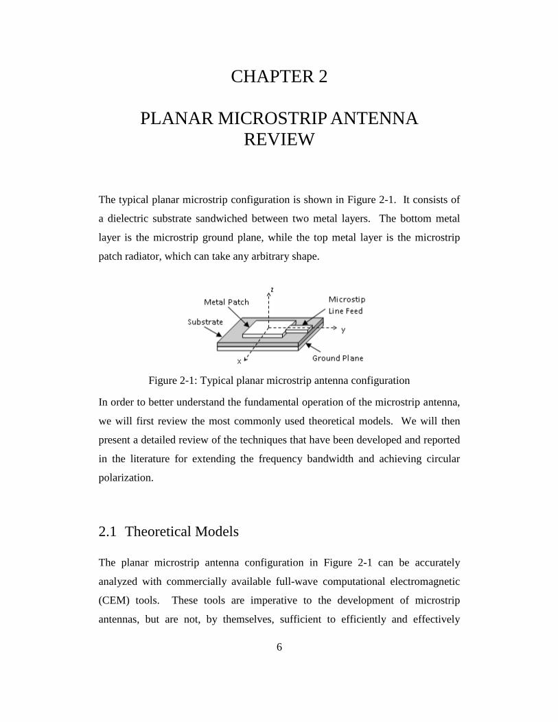
The typical planar microstrip configuration is shown in Figure 2-1. It consists of
a dielectric substrate sandwiched between two metal layers. The bottom metal
layer is the microstrip ground plane, while the top metal layer is the microstrip
patch radiator, which can take any arbitrary shape.
Figure 2-1: Typical planar microstrip antenna configuration
In order to better understand the fundamental operation of the microstrip antenna,
we will first review the most commonly used theoretical models. We will then
present a detailed review of the techniques that have been developed and reported
in the literature for extending the frequency bandwidth and achieving circular
polarization.
2.1 Theoretical Models
The planar microstrip antenna configuration in Figure 2-1 can be accurately
analyzed with commercially available full-wave computational electromagnetic
(CEM) tools. These tools are imperative to the development of microstrip
antennas, but are not, by themselves, sufficient to efficiently and effectively

7
design a planar microstrip antenna. A more fundamental understanding of the
physics that explain the operation of the microstrip antenna is key to reducing
design time and improving overall performance. Two of the most common
models for achieving this fundamental understanding are the cavity model and the
transmission line model.
2.1.1 Cavity model
The cavity model was first introduced by Lo et al. [2] at the University of Illinois
at Urbana-Champaign. Lo et al. recognized that the narrow band nature of the
microstrip antenna warranted its modeling as a lossy cavity resonator. When
analyzing a planar microstrip antenna using the cavity model, each TEmn and
TMmn mode is individually solved for based on the following assumptions for thin
substrate antennas (h << λo):
• The fields in the interior region do not vary with z 0z
∂ ≡ ∂ .
• The E-field is only z-directed.
• The H-field has transverse components only in the region bound by patch
metalization and the ground plane.
• The electric current has no component normal to the edges of the patch
metalization.
The final assumption listed allows us to model the sides of the microstrip antenna
cavity as perfect magnetic walls because the tangential component of the H-field
at these walls is negligible.
The cavity model accounts for all modes of the antenna when calculating the
input impedance. The effects of radiation and other antenna losses on the input
impedance are often included by artificially increasing the substrate loss tangent
or by enforcing impedance boundary conditions at the radiating walls [3]. The
overall implementation of the cavity model is often complex and somewhat

8
computationally intense due to the use of Green’s functions and numerical
integration. For more information on the cavity model please see references [2-
5].
2.1.2 Transmission line model
The transmission line model was first proposed by Munson [1] and later improved
by Derneryd [6] and Pues and Van de Capelle [7]. Its usefulness is typically
limited to rectangular or square patches, but extensions to other shapes are
possible. The rectangular transmission line model is schematically depicted in
Figure 2-2 per the Pues and Van de Capelle model. In this model, Ys is the self-
admittance of the open-end of the patch, and Ym is the mutual admittance. The
mutual admittance, Ym, accounts for the not only the coupling between the two
radiating edge slots, but also the impact of the two non-radiating edge slots.
Figure 2-2: Improved rectangular microstrip patch three-port transmission line
model
The model in Figure 2-2 can be further improved by adding the effects of the feed
at port 3. In the case of a microstrip line feed, the feed is simply added as a
transmission line of length equal to the length of the feed and characteristic
impedance equal to that of the feed line. In the case of a probe feed, however,
simple transmission line equations are inadequate due to the unknown
characteristic impedance of the probe. Often, the probe feed is modeled as an
infinite line charge in order to ascertain its impedance. This method assumes a
patch and ground plane of infinite extent such that applying image theory to the

9
probe feed yields an infinite line charge. This and other probe models are
discussed in further detail in the literature [3-5, 8].
In order to derive the slot parameters of the TLM, two concepts are employed:
• the open end concept
• the equivalent slot concept.
The open end concept extends the effective length of the microstrip line due to the
fringing fields at the open end and is used to compute the Im(Ys), or self-
susceptance (Bs). The equivalent slot concept evaluates the radiation of the
equivalent slot to determine the Re(Ys), or self-conductance (Gs). Analytic
expressions are given by [4]
( )tan Ss cB Y β= (2.1)
( )2 2
2 3
1 sin 1 cos sin cos 2 124 12 3s
w s s w wG w Si w ww w wπη
≈ + + − × − + + − (2.2)
where Yc is the characteristic admittance, β is the propagation constant of the
microstrip line, S is the open-end microstrip line extension, η is the free space
impedance, w is the normalized slot length (koWe), s is the normalized slot width
(koS), ko is the free space wave number, and 0
sin( )x uSi x du
u= ∫ .
Multiplying the above self-admittance values by auxiliary coupling functions
gives the mutual admittance of the radiating slots [4].
𝐺𝑚 = 𝐺𝑠𝐹𝑔𝐾𝑔 (2.3)
𝐵𝑚 = 𝐵𝑠𝐹𝑏𝐾𝑏 (2.4)
The conductance, 𝐹𝑔𝐾𝑔, and susceptance, 𝐹𝑏𝐾𝑏, auxiliary coupling functions are
given by [4]

10
( ) ( )2
0 2224gsF J l J l
s= +
− (2.5)
𝐾𝑔 = 1 (2.6)
( ) ( )2
0 22
2
2
242 3 12ln
2 2 24
b
e
sY l Y lsF
ss Cs
π +−=
+ − + −
(2.7)
𝐾𝑏 = 1 − 𝑒−0.21𝑤 (2.8)
where Jn and Yn are Bessel functions, l is the normalized center distance between
slots (ko(L1+L2+S)), s is the normalized slot width (koS), w is the normalized slot
length (koWe), ko is the free space wave number, and Ce is Euler’s constant
(0.577216). For further explanation of these variables, please see [4, pp. 527-
578].
The transmission line model of the microstrip patch antenna provides a simple
means to calculate the input impedance of the antenna using basic microwave
engineering. However, the transmission line model, as presented, only considers
the fundamental mode of the antenna. This can be an issue for electrically large
patches or patches with parasitic shorting pins or slots. Consequently, we will
have to be aware of this limitation when utilizing this transmission line model.
2.2 Techniques for Extending Bandwidth
The frequency bandwidth of an antenna may be defined by its input voltage
standing wave ratio (VSWR), its radiation pattern (beamwidth, gain, sidelobe
level), or its polarization. All of these performance parameters vary with
frequency, and depending on the requirements for a given application, any one of
them could be the limiting factor that determines the frequency bandwidth. In
practice, however, the radiation pattern of a single microstrip antenna is broad and
well behaved as a function of frequency, whereas the input VSWR varies

11
significantly with frequency. The polarization also varies appreciably with
frequency, but typically not as significantly as the input VSWR. As such, it is the
input VSWR that typically limits the frequency bandwidth of a microstrip
antenna. For this reason, this section will focus on the techniques that have been
commonly employed in the literature to increase the input VSWR bandwidth.
2.2.1 Substrate parameters
The substrate parameters that have an effect on the input VSWR bandwidth
include the relative permittivity (εr) and the substrate height (h). A decrease in
the εr or an increase in substrate height results in a lower amount of stored energy
in the substrate between the patch radiator and ground. This leads to a
corresponding decrease in the quality factor, Q, which in turn results in an
increase of the input VSWR bandwidth per the relation
VSWRQVSWRBW 1−
= , where LostPower
StoredEnergy =Q (2.9)
The attainable benefit from increasing the substrate thickness and lowering
substrate εr is limited by the onset of surface waves, increased parasitic feed
radiation, and higher order modes that may develop. In practical application, this
limit is achieved as h approaches 0.02 λ [3, pp. 534-538].
2.2.2 Feed method
The microstrip patch radiator can be excited using a direct probe feed, a direct
edge feed, a proximity coupled feed, or an aperture coupled feed as shown in
Figure 2-3. Selecting which type of feed to use depends on the requirements of
the antenna. The direct probe and edge feeds offer the following benefits:
• lower back lobe radiation compared to a coupled microstrip line that
induces back radiation from the microstrip feed, and

12
• lower cost due to simpler construction (one less metal layer).
The proximity coupled feed offers the following benefits:
• lower back lobe radiation compared to a coupled microstrip line that
induces back radiation from the microstrip feed, and
• increased input VSWR bandwidth due to the additional tuning available
from the coupled feed geometry.
The aperture coupled feed offers the following benefits:
• increased input VSWR bandwidth due to the additional tuning available
from the coupled feed geometry, and
• lower cross polarization due to the shielding of stray feed radiation by the
ground plane.
Figure 2-3: Microstrip patch radiator excitation methods: (a) direct probe, (b)
direct edge, (c) proximity coupled and (d) aperture coupled
Of the feed types depicted in Figure 2-3, the aperture coupled feed is superior to
all others in terms of extending the input VSWR bandwidth of microstrip
antennas. The aperture coupled feed was introduced in 1985 by Pozar [9]. The
wide input VSWR bandwidth is attributed to the fact that the aperture coupled
configuration permitted the use of a thick antenna substrate, thus lowering the Q
of the microstrip antenna. In addition, the aperture itself can be designed to
resonate along with the patch producing a wide input VSWR bandwidth.

13
2.2.3 Parasitic stacked patch
A parasitic stacked patch takes advantage of the coupling between stacked
resonators to extend the input VSWR bandwidth of microstrip antennas. A cross
sectional view of a probe fed parasitic stacked patch antenna is shown in Figure
2-4. Designing the top parasitic patch such that it has a slightly different size or
resonance than the bottom driven patch provides multi-resonant behavior that
extends the VSWR bandwidth.
Figure 2-4: Probe fed parasitic stacked patch antenna cross section
The parasitic stacked patch has been extensively studied in the literature. It was
first introduced by Sabban [10] in 1983. Sabban published empirical results
showing input VSWR 2:1 bandwidths ranging from 9 to 15 percent for both linear
and circular polarization designs at S and X band. This is a 10X improvement
compared to typical single probe fed patch results.
In 1984, Chen et al. [11] investigated the performance of a probe fed circular
parasitic stacked patch with respect to the patch metal separation (S) and the ratio
of the parasitic to the driven patch diameter
d
pD
D . The authors performed
experiments with Dp > Dd, and noted that with increasing S, the ratio of the patch
diameters approached unity. This suggests that wider band performance is
achieved when the separation, S, between patches is smaller. Practically, the
bandwidth must decrease and approach that of a single patch as S goes to zero.

14
Therefore, the authors’ results simply indicate that there is an optimal value for S
that is smaller than the smallest S investigated (3.81 mm). The best reported input
VSWR 2:1 impedance bandwidth Chen et al. measured was just over 20% for a
linear polarization C-band antenna. The authors did note that the radiation pattern
of the linear polarization antenna exhibited a broad 3 dB beamwidth of
approximately 90° and an almost equal E- and H-plane pattern. The former helps
improve scan loss in an electronically scanned array and the latter suggests that
the circular parasitic stacked patch will make a good circular polarization (CP)
radiator.
More recently (2009), Elkorany et al. [12] reported an ultra-wideband rectangular
parasitic stacked patch antenna that achieved an input VSWR 2:1 bandwidth of
86% (5.6 – 14.2 GHz). The authors claim that the use of a large parasitic patch
size compared to that of the driven patch size provides this significant increase in
bandwidth. A square 2 mm x 2 mm driven patch was used to excite a square 20
mm x 20 mm parasitic patch in a series of Ansys HFSS simulations. The
substrates utilized in the simulations were 80 mm x 80 mm with εr1 = 2.2, εr2 =
4.6, h1 = 3.5 mm and S = 2 mm. Given the physical construction of the antenna,
the driven patch appears to be too small to exhibit resonance. Assuming a
permittivity of 2.2, the driven patch is only one-tenth of a wavelength square at
the highest operating frequency of 14.2 GHz. Therefore, the driven patch is not
resonant, and the fundamental principle that helps broaden the input VSWR of
this antenna is not that of multiple coupled resonators. The performance, in this
case, can be attributed to the feed type. The feed is a top-loaded probe feed that is
proximity coupled to the patch radiator.
2.2.4 Slots in patch metal
A slot can be placed in the patch metal to extend the input VSWR bandwidth of
the microstrip patch antenna. The slot is designed such that it is resonant near the
resonance of the patch. The frequency and Q of the slot and patch resonances can

15
be adjusted independently providing the designer the freedom to maximize the
input VSWR bandwidth.
A U-Slot microstrip patch, Figure 2-5, has been studied extensively for its ability
to achieve broadband performance [13-14, 16-18]. The benefit inherent in the U-
Slot microstrip patch is its ability to excite multiple resonances to achieve wide
bandwidth without increasing the size and fabrication complexity of the
microstrip antenna by adding parasitically coupled patch resonators.
The U-Slot microstrip patch was first introduced by Huynh et al. [13] in 1995. In
this paper, the authors presented empirical results of a probe-fed, rectangular U-
Slot microstrip patch that achieved an input VSWR 2:1 bandwidth of
approximately 47% (812 – 1282 MHz). The patch metal to ground height, h, of
this U-Slot microstrip patch was 1.06 inches, which corresponds to 0.07 to 0.12
wavelengths over the input VSWR 2:1 bandwidth. This is much larger than the
practical height limit of 0.02 wavelengths for a conventional microstrip antenna.
The addition of the U-Slot transforms the input impedance of the microstrip
antenna such that there is no appreciable inductive component, thus permitting
electrically thick probe-fed designs that offer inherently wider bandwidths.
However, the addition of the U-Slot does narrow the beamwidth and cause a
noticeable asymmetry in the y-z plane radiation pattern, both of which are
detrimental to the design of low loss, wide electronic scan arrays.

16
Figure 2-5: U-Slot microstrip antenna
In 2003, Weigand et al. [14] presented an analysis of the U-Slot antenna that
utilized former experiments, method of moments (MoM) simulations and
measurement results to develop a set of design rules. The authors attempted to
isolate the features of the U-Slot antenna that dominated each of the four
resonances (jX = 0) observed in the complex S-parameters of the antenna. The
first resonance was dominated by the total U-Slot length (2C+D) and, to a lesser
extent, the B-dimension of the patch. The second resonance was dominated by
the B-dimension of the patch and the D-dimension of the slot. Analysis of the
surface currents on the patch at the second resonance shows a high distribution of
y-directed currents consistent with a TM01 patch mode. The third resonance was
not dominated by any one feature and exhibited both x- and y-directed surface
currents resulting in high cross-polarization levels. The authors noted that low
cross-polarization could be achieved if the following conditions were met.

17
75.0≥DC and 3.0≥A
C (2.10)
The fourth resonance was dominated by the slot dimensions and location, and can
attributed to the pseudo-patch formed by the U-Slot. The authors went on to
present a design procedure that they further used to successfully design multiple
U-Slot antennas with fractional impedance bandwidths of up to 40%.
2.3 Methods for Achieving Circular Polarization (CP)
There are two feed methods typically used to obtain circular polarization (CP) in
microstrip patch radiators: (1) dual-orthogonal feed and (2) single feed. In a dual-
orthogonal fed microstrip patch, two separate feeds are used to excite orthogonal
modes in phase quadrature. The first feed excites the TM01 mode, while the
second feed excites the TM10 mode. A quadrature phase is introduced between
the two excitations within the feed network supplying the antenna. In a singly fed
microstrip patch, a single feed is positioned within the patch such that it alone
excites two orthogonal patch modes with equal amplitude and in phase
quadrature. The singly fed CP microstrip antenna has the advantage of lower loss
due to less feed complexity, but the dual-orthogonal fed microstrip antenna
typically has a broader CP bandwidth. The remainder of this section provides
examples of planar microstrip antenna techniques that have been implemented to
achieve wide CP bandwidth.
In 1993, Targonski and Pozar [15] introduced the design of a dual-orthogonal
feed, circularly polarized aperture coupled microstrip antenna that achieved wide
impedance and axial ratio bandwidth. The wide impedance bandwidth was
achieved by employing (1) a thick (0.087λo), low dielectric foam microstrip patch
substrate, (2) an aperture coupled crossed slot, and (3) a multi-resonant structure
(both the patch and slot were resonant). The authors needed to make the slot
resonant to achieve adequate coupling to the patch given the thick substrate, but

18
this also resulted in an undesired increase in the back lobe radiation. The wide
axial ratio bandwidth was achieved through the use of physical symmetry in the
dual-orthogonal feed. The authors fed the resonant crossed slot with two different
coupled feed architectures: (1) series feed (Figure 2-6a) and (2) parallel feed
(Figure 2-6b). The series feed architecture provides simpler construction with a
wide input VSWR 2:1 bandwidth. However, the series feed is not inherently as
symmetric as the parallel feed, which results in a much reduced axial ratio
bandwidth that is more sensitive to slot and feed construction errors. Given the
symmetry of the parallel feed design and the fact that Wilkinson power divider
networks are employed to maintain similar excitation magnitudes on the arms of
the crossed slot, the parallel feed architecture achieves extremely wide axial ratio
bandwidths. In fact, the limiting factor for CP bandwidth of the parallel feed is
not axial ratio, but rather the loss of gain in the radiation pattern due to absorptive
losses in the resistors of the Wilkinson dividers. The authors presented a single
series fed design that yielded 30% and 12% of input VSWR 2:1 bandwidth and 3
dB axial ratio bandwidth respectively. The authors presented two parallel fed
designs that yielded greater than 50% of input VSWR 2:1 bandwidth with a CP
bandwidth of 22% and 29%, per the definition of being within 1 dB of the
maximum radiation pattern gain over the band.

19
(a)
(b)
Figure 2-6: Microstrip symmetric crossed slot (a) series and (b) parallel feeds for CP [15]
In 2007, Tong and Wong [16] introduced the design of a single feed, circularly
polarized U-Slot microstrip antenna that achieved good CP performance. The
benefit of the antenna was its inherent simplicity. It was a simple two-layer probe
fed patch on a thick (0.085λo) foam substrate with an asymmetric U-Slot to excite
the two orthogonal modes. The authors achieved a 9% and 4% input VSWR 2:1
bandwidth and 3 dB axial ratio bandwidth respectively.
In 2008, Yang et al. [17] studied the effects of substrate thickness on the
impedance and axial ratio bandwidths of single feed, circularly polarized
truncated corner square microstrip antennas. The authors found that the use of
thicker, lower permittivity substrates was the main reason for increases in the
impedance bandwidth. In order to achieve thicker substrates, though, the authors
needed to compensate for the high inductance of the probe feed. Two techniques,
a U-Slot in the patch and an L-probe feed, were used to add capacitance to

20
compensate for the high inductance of the probe feed. The four patch
configurations in Figure 2-7 were studied via simulation and measurement. The
best result the authors were able to achieve was a 19% and 14% input VSWR 2:1
bandwidth and 3 dB axial ratio bandwidth respectively using an L-probe feed
configuration on a 0.2λo thick substrate.
In 2011, Lam et al. [18] presented a miniaturized single feed, circularly polarized
truncated corner square microstrip antenna using the U-Slot configuration shown
in Figure 2-7(b). The authors used a high dielectric substrate (εr = 10.2) to
miniaturize the x-y dimensions of the patch by a factor of nearly three, yielding a
patch length and width of 0.13λo. The height of the substrate, however, was only
decreased by a factor of less than two, yielding a patch substrate height of 0.05λo.
The capacitance of the U-Slot enabled the electrically large substrate height by
compensating for the inductance of the feed. With this configuration, the authors
achieved a 15% and 3% input VSWR 2:1 bandwidth and 3 dB axial ratio
bandwidth, respectively.
2.4 Summary Remarks
The body of work openly available in the literature for planar microstrip antennas
is extensive. A practicing antenna engineer could readily find design approaches
and techniques for achieving wide bandwidth and desired radiation characteristics
such as circular polarization. As we will see in the next chapter, however, the
body of work surrounding cylindrical microstrip antennas is significantly less
providing minimal useful information to the practicing antenna engineer.

21
(a) Probe Fed (b) Probe Fed, U-Slot
(c) L-Probe Fed, U-Slot (d) L-Probe Fed Figure 2-7: Single feed, circularly polarized truncated corner square microstrip patch
configurations studied by Yang et al. [17]

22
CHAPTER 3
CYLINDRICAL MICROSTRIP ANTENNA REVIEW
The cylindrical microstrip antenna is the most common embodiment of a broader class of
conformal antennas known as singly curved conformal microstrip antennas (SC-CMA). A probe
fed cylindrical rectangular microstrip antenna (CRMA) is depicted in Figure 3-1. A metal
cylinder of radius a forms the ground plane of the CRMA. A substrate of height h and
permittivity 𝜀1 extends completely around the body of the metal cylinder. The rectangular patch
metal is printed on the surface of the substrate. The width and length of the patch metal are
given by 2W = 2(a+h)φo and 2L, respectively. The patch metal is covered by a superstrate that
acts as a radome to protect the patch metal. The superstrate wraps completely around the metal
cylinder and substrate with a thickness t and permittivity 𝜀2.
Figure 3-1: Cylindrical rectangular microstrip antenna (CRMA)

23
3.1 Modes
The CRMA depicted in Figure 3-1 supports two fundamental orthogonal modes: TM01 and TM10.
The TM01 mode is defined by axial currents that radiate an E-field that is predominantly z-axis
directed. To excite the TM01 mode, the feed is positioned such that φ𝑝 equals 90°. The value of
zp determines the input impedance match. The TM10 mode is defined by circumferential currents
that radiate an E-field that is predominantly x-axis directed. To excite the TM10 mode, the feed
is positioned such that zp equals zero. The value of φ𝑝 determines the input impedance match.
3.2 Theoretical Models
Theoretical models are needed for the accurate analysis of the CRMA. Given the complexity of
the physical CRMA, it is important to have a computationally efficient model that allows a
practicing engineer to gain insight into the fundamental operation of the antenna. This section
reviews the state of current literature with respect to models for the analysis of the CRMA.
3.2.1 Full-wave 3D model
The CRMA configuration in Figure 3-1 can be accurately analyzed with commercially available
full-wave CEM tools. These tools, most notably Ansys HFSS, will be used extensively to
analyze the performance and behavior of the CRMA. However, it can be difficult to gain
significant physical insight into the operation of the antenna if one relies solely on these tools. In
addition, full-wave models are often computationally expensive in terms of time and computing
resources. As was the case with the planar microstrip antenna, a more fundamental
understanding of the physics that explain the operation of the CRMA is key to reducing design
time and improving overall performance.
3.2.2 Cavity model
The cavity model for the cylindrical microstrip antenna, like that of the planar microstrip
antenna, is based on the theories that were first introduced by Lo et al. [2] at the University of

24
Illinois at Urbana-Champaign. When analyzing the CRMA using the cavity model, each TEmn
and TMmn mode is individually solved for based on the following assumptions for thin substrate
antennas (h << λo):
• The fields in the interior region do not vary with ρ 0ρ
∂≡ ∂
.
• The E-field is only ρ-directed.
• The H-field has transverse components only in the region bound by patch metalization
and the ground plane.
• The electric current has no component normal to the edges of the patch metalization.
The final assumption listed allows us to model the sides of the microstrip antenna cavity as
perfect magnetic walls because the tangential component of the H-field at these walls is
negligible.
The cavity model has been used extensively within the literature [19-27] to efficiently compute
the resonant frequency, Q factor (fractional bandwidth), and radiation patterns of the CRMA.
An excellent summary of much of this work can be found in a text written by Kin-Lu Wong [19].
In this text, Wong provides cavity model solutions for both probe fed and slot coupled
cylindrical microstrip antennas. In the case of a probe fed CRMA, the resonant frequency of the
antenna is given by [19]
2 2
02 22mnc m nf
b Lφε
= +
(3.1)
where b = (a+h) in Figure 3-1. As was the case with the planar cavity model, the overall
implementation is often complex and somewhat computationally intense due to the use of
Green’s functions and numerical integration.

25
3.2.3 Generalized Transmission Line Model (GTLM)
The generalized transmission line model (GTLM) for microstrip patch antennas was first
proposed by Bhattacharyya [28]. It is applicable for microstrip patches of any configuration,
where the separation of variables is possible in the wave equation expressed in the particular
coordinate system. When analyzing a microstrip antenna using the GTLM, a single index
transmission line mode, such as TMm, is determined where
m mnn
TM TM= ∑ (3.2)
The characteristics of a specific resonant mode, TMmn, are obtained from characteristics of the
TMm mode near the resonant frequency of the specific mode.
For the case of a probe-fed CRMA, the GTLM is schematically depicted in Figure 3-2 [19]. In
this schematic model, A, B and C denote the positions z = L, z = -L, and z = zp (probe location in
z); g’1, g’2 and g’3 are the elements of a π-network that represents the section of transmission line
between z = L and z = zp; g1, g2 and g3 are the elements of a π-network that represents the section
of transmission line between z = zp and z = -L. The variables ys and ym represent the self- and
mutual admittance of the radiating edge of the microstrip patch, respectively. A detailed
derivation for the variables in the schematic for the TMm mode of the probe-fed CRMA is given
in reference [19].
Figure 3-2: GTLM schematic for a probe-fed CRMA

26
3.3 Summary Remarks
The body of work openly available in the literature for cylindrical microstrip antennas is limited.
Most works focus on the modeling and analysis of the structure, but provide little practical
information for the practicing antenna design engineer. In the chapters to follow, a detailed
analysis of the cylindrical rectangular microstrip antenna (CRMA) is carried out with a focus on
developing a practical CRMA transmission line model (TLM) and design approach. The goal is
to provide a basic understanding of CRMA performance as the patch metal bend radius becomes
electrically small. In order to do this, we will first perform an extensive parametric study of the
patch metal bend radius of the CRMA using Ansys HFSS, a full-wave 3D finite element
(FEM) analysis tool.

27
CHAPTER 4
CRMA FULL-WAVE 3D ANALYSIS
In this chapter, the details of a full-wave 3D electromagnetic analysis of the cylindrical
rectangular microstrip antenna (CRMA) are presented. The analysis focuses on expanding the
understanding of the impact the patch metal bend radius has on the performance of the CRMA.
Specifically, we are interested in quantifying the impedance bandwidth, resonant frequency and
excitation location of a probe fed CRMA as the patch bend radius is made electrically small. To
that end, models were created in Ansys HFSS to independently analyze the TM01 (axial) and
TM10 (circumferential) modes of the CRMA as the patch metal bend radius varied from planar to
approximately 0.15λo. Existing works within the literature have analyzed the CRMA at various
cylinder bend radii, but none, to the author’s knowledge, have quantified these important
performance parameters at such small patch metal bend radii.
4.1 Full-Wave 3D Analysis Approach
A full-wave 3D analysis was performed using the Ansys HFSS finite element method (FEM)
iterative solver. A square CRMA, where 2W = 2L per Figure 3-1, was chosen for the analysis
due to the eventual desire to radiate a circularly polarized field. The CRMA was designed to
achieve 50 Ω resonance near the GPS L1 band at 1575 MHz.
As a first step in the analysis, the accuracy of the Ansys HFSS CRMA model requires
validation. Typically, simulation results from the model are compared to that of actual
measurements to validate model accuracy. In this case, however, the fabrication of conformal
antennas is difficult so an alternate approach is taken. The patch metal bend radius of the
CRMA, b in Figure 3-1, is set to 100 inches, and the TM01 and TM10 modes are analyzed. Since

28
the antenna is nearly planar, the two modes should yield nearly identical results. In addition, a
planar microstrip antenna model with the same physical construction as the CRMA is analyzed
in Ansys HFSS. If the planar microstrip antenna and CRMA simulation results are nearly
identical, the CRMA model is considered accurate and suitable for use in the full-wave study.
Once the Ansys HFSS model is validated, a parametric study of the effect of the patch metal
bend radius on the TM01 (axial) and TM10 (circumferential) modes of the CRMA is performed.
Five different patch metal bend radii (b = 1.075”, 1.75”, 3.625”, 7.375” and 9.875”) plus a planar
embodiment are modeled and simulated at L-band near 1575 MHz. Referring to Figure 3-1,
other than the patch metal bend radius, b, the only parameters that changed from one model to
the next are
1) φ0, which is varied to keep the size of the patch metal, 2𝑏φ0, constant, and
2) the probe position, φ𝑝, 𝑧𝑝, which is varied to achieve 50Ω resonance.
In practice, the conformal antenna is often placed in a cavity rather than allowed to wrap around
the platform like the CRMA. Therefore, the parametric study of the patch metal bend radius that
was performed on the CRMA will also be performed on two cavity backed (CB) CRMA designs
at L-band near 1575 MHz. The first CB-CRMA has the same dielectric construction as the
CRMA, while the second CB-CRMA has different dielectric construction and physical patch
dimensions. Comparing the CB-CRMA analysis results to that of the CRMA, we will be able to
determine if the cavity, substrate permittivity or physical patch size have any effect on relative
performance as a function of patch metal bend radius.
4.2 Ansys HFSS CRMA Models
The HFSS model for the CRMA is shown in Figure 4-1. The CRMA consists of a dielectric
substrate, a square metal patch, a probe feed, and a dielectric superstrate or radome. The
substrate and superstrate wrap around a perfectly conducting cylinder with hemispherical end
caps. A vacuum filled box surrounds the entire structure, and PML (perfectly matched layer)
boundaries are employed on the walls of the vacuum filled box for accuracy.

29
The HFSS model for the CB-CRMA is shown in Figure 4-2. The CB-CRMA consists of a
dielectric substrate, a square metal patch, a probe feed, and a dielectric superstrate or radome.
The substrate and superstrate fill the extent of the cavity, but do not wrap around the perfectly
conducting cylinder. A vacuum filled box surrounds the entire structure, and PML boundaries
are employed on the walls of the vacuum filled box for accuracy.
Figure 4-1: HFSS CRMA model
Figure 4-2: HFSS Cavity backed (CB) CRMA model
30
4.3 Ansys HFSS Results
4.3.1 Model validation
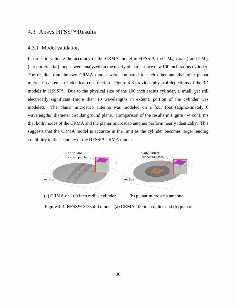
In order to validate the accuracy of the CRMA model in HFSS, the TM01 (axial) and TM10
(circumferential) modes were analyzed on the nearly planar surface of a 100 inch radius cylinder.
The results from the two CRMA modes were compared to each other and that of a planar
microstrip antenna of identical construction. Figure 4-3 provides physical depictions of the 3D
models in HFSS. Due to the physical size of the 100 inch radius cylinder, a small, yet still
electrically significant (more than 10 wavelengths in extent), portion of the cylinder was
modeled. The planar microstrip antenna was modeled on a four foot (approximately 6
wavelengths) diameter circular ground plane. Comparison of the results in Figure 4-4 confirms
that both modes of the CRMA and the planar microstrip antenna perform nearly identically. This
suggests that the CRMA model is accurate in the limit as the cylinder becomes large, lending
credibility to the accuracy of the HFSS CRMA model.
(a) CRMA on 100 inch radius cylinder (b) planar microstrip antenna
Figure 4-3: HFSS 3D solid models (a) CRMA 100 inch radius and (b) planar

31
Figure 4-4: Comparison of input impedance CRMA 100 inch radius to planar
4.3.2 Parametric analysis
4.3.2.1 CRMA The CRMA parametric analysis results were obtained from the HFSS model shown in Figure
4-1. The TM01 (axial) and TM10 (circumferential) modes of the CRMA both exhibit a well
behaved single resonance, but their impedance bandwidth and resonance frequency are quite
different. The TM01 mode input impedance locus for the 1.75 inch patch metal bend radius
exhibits an input VSWR 2:1 bandwidth of 23 MHz or nearly 1.5% at the resonance frequency of
1546 MHz as shown on the Smith chart in Figure 4-5. The TM10 mode input impedance locus
for the 1.75 inch patch metal bend radius exhibits an input VSWR 2:1 bandwidth of 11 MHz or
nearly 0.7% at the resonance frequency of 1600 MHz as shown on the Smith chart in Figure 4-6.
32
In addition to the electrical differences in the two modes, the probe feed offset from center is
physically greater for the TM01 mode.
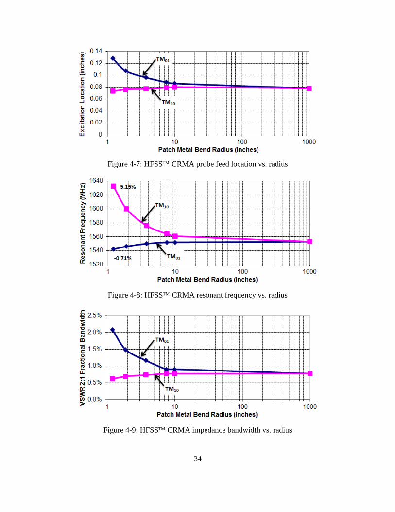
A full characterization of the CRMA TM01 and TM10 modes as a function of patch metal bend
radius reveals significant differences in the modes due to the inherent asymmetry of the
structure. The probe feed offset location of the TM01 mode increases over 60% as the patch
metal bend radius decreases from infinite (planar) to 1.075” (~0.15λ) as shown in Figure 4-7.
The probe feed offset location of the TM10 mode, on the other hand, changes in the opposite
direction, decreasing by nearly 10% over the same range of patch metal bend radii. Similar
trends are seen in the resonant frequency as the TM10 mode resonance increases by more than
5% compared to a slight decrease of about 0.7% for the TM01 mode as shown in Figure 4-8.
This trend suggests that the circumferential patch dimension, 2W in Figure 3-1, must be made
increasingly larger than the axial patch dimension, 2L in Figure 3-1, as the patch metal bend
radius decreases to achieve the same resonant frequency. Finally, the TM01 input VSWR 2:1
bandwidth more than doubles as the patch metal bend radius decreases, while the TM10 mode
bandwidth slightly decreases as shown in Figure 4-9.
Having quantified the performance of the CRMA as a function of patch metal bend radius, we
will move on to the analysis of a cavity backed (CB) CRMA, see Figure 4-2. The CB-CRMA is
of particular interest as many real world applications require the antenna to mount within a
cavity for aerodynamics or space constraint purposes.

33
Figure 4-5: HFSS CRMA TM01 example Smith chart results from 1 to 2 GHz
Figure 4-6: HFSS CRMA TM10 example Smith chart results from 1 to 2 GHz
34
Figure 4-7: HFSS CRMA probe feed location vs. radius
Figure 4-8: HFSS CRMA resonant frequency vs. radius
Figure 4-9: HFSS CRMA impedance bandwidth vs. radius

35
4.3.2.2 Cavity Backed CRMA Two CB-CRMA designs are analyzed to provide insight into the impact of the cavity as well as
the dielectric properties of the antenna substrate. The CB-CRMA Design #1 uses identical
substrate materials to the previously analyzed CRMA and serves to look not only at the impact of
the cavity on performance as a whole, but also whether said cavity alters the performance trends
as a function of patch metal bend radius as seen in Figure 4-7 to Figure 4-9 for the CRMA. The
CB-CRMA Design #2 uses a much lower dielectric constant substrate of 3.0 compared to that of
the CRMA and CB-CRMA Design #1, which both use a dielectric constant 16.0 material. This
lower dielectric constant design requires a much larger patch metal size, which serves to confirm
whether the patch metal extent has any significant impact on the performance trends as a
function of patch metal bend radius.
4.3.2.2.1 Design #1 The CB-CRMA parametric analysis results were obtained from Design #1 of the HFSS model
shown in Figure 4-2. Like the CRMA, the TM01 (axial) and TM10 (circumferential) modes of the
CB-CRMA Design #1 both exhibit a well behaved single resonance, but their impedance
bandwidth and resonance frequency are quite different. The TM01 mode input impedance locus
for the 1.75 inch patch metal bend radius of Design #1 exhibits an input VSWR 2:1 bandwidth of
11 MHz or nearly 0.7% at the resonance frequency of 1579 MHz as shown on the Smith chart in
Figure 4-10. The TM10 mode input impedance locus for the 1.75 inch patch metal bend radius of
Design #1 exhibits an input VSWR 2:1 bandwidth of 5 MHz or nearly 0.31% at the resonance
frequency of 1620 MHz as shown on the Smith chart in Figure 4-11. In addition to the electrical
differences in the two modes, the probe feed offset from center is physically greater for the TM01
mode.
A full characterization of the CB-CRMA Design #1 TM01 and TM10 modes as a function of patch
metal bend radius reveals significant differences in the modes due to the inherent asymmetry of
the structure. The probe feed offset location of the TM01 mode increases over 60% as the patch
metal bend radius decreases from infinite (planar) to 1.075” (~0.15λ) as shown in Figure 4-12.
The probe feed offset location of the TM10 mode, on the other hand, changes in the opposite
direction, decreasing by nearly 10% over the same range of patch metal bend radii. Similar

36
trends are seen in the resonant frequency as the TM10 mode resonance increases by more than
3.5% compared to a slight decrease of about 0.7% for the TM01 mode as shown in Figure 4-13.
This trend suggests that the circumferential patch dimension, 2W in Figure 3-1, must be made
increasingly larger than the axial patch dimension, 2L in Figure 3-1, as the patch metal bend
radius decreases to achieve the same resonant frequency. Finally, the TM01 input VSWR 2:1
bandwidth more than doubles as the patch metal bend radius decreases, while the TM10 mode
bandwidth slightly decreases as shown in Figure 4-14.
The only physical difference in the structure of the CB-CRMA Design #1 and the CRMA is the
addition of the cavity. Comparing CB-CRMA Design #1 results to those of the CRMA, it is
evident that the cavity changes the performance of the CRMA. The cavity causes the probe feed
excitation location to move closer to the center of the patch, while the resonant frequency
increases by one to two percent. The biggest effect of the cavity, though, is a roughly halving of
the VSWR 2:1 input impedance bandwidth. Despite the significant impact of the cavity on the
performance of the CRMA, the relative performance changes as a function of patch metal bend
radius are nearly identical suggesting that the impact of the cavity does not change as a function
of the patch metal bend radius.
Figure 4-10: HFSS CB-CRMA Design #1 TM01 example Smith chart results from 1 to 2 GHz

37
Figure 4-11: HFSS CB-CRMA Design #1 TM10 example Smith chart results from 1 to 2 GHz
Figure 4-12: HFSS CB-CRMA Design #1 probe feed location vs. radius
Figure 4-13: HFSS CB-CRMA Design #1 resonant frequency vs. radius

38
Figure 4-14: HFSS CB-CRMA Design #1 impedance bandwidth vs. radius
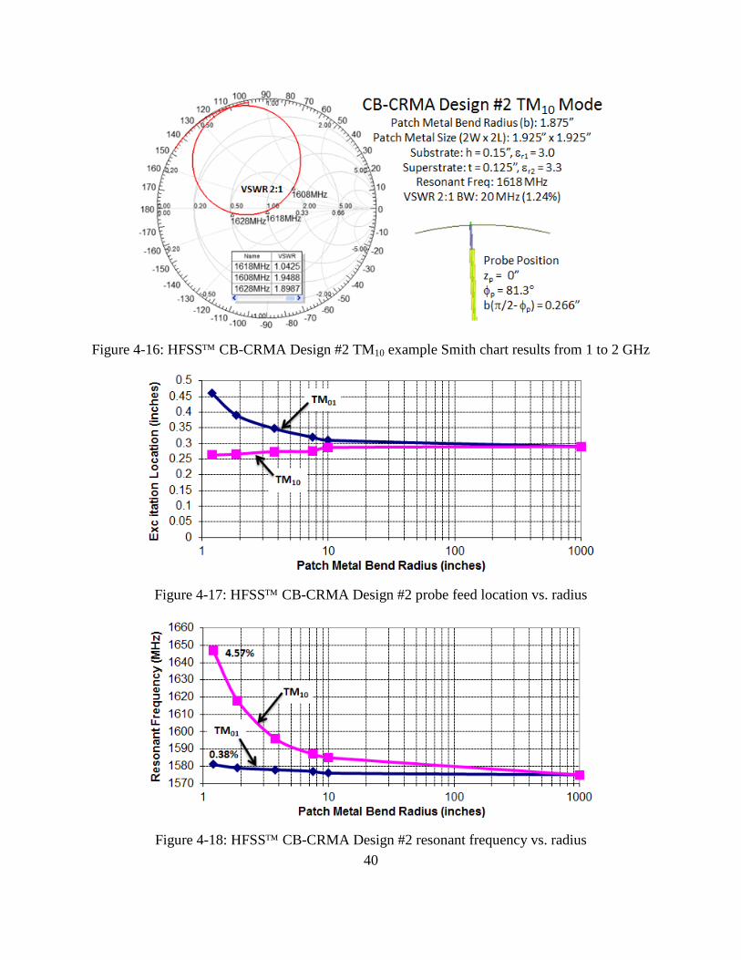
4.3.2.2.2 Design #2 The CB-CRMA parametric analysis results were obtained from Design #2 of the HFSS model
shown in Figure 4-2. Like the CRMA and CB-CRMA Design #1, the TM01 (axial) and TM10
(circumferential) modes of the CB-CRMA Design #2 both exhibit a well behaved single
resonance, but their impedance bandwidth and resonance frequency are quite different. The
TM01 mode input impedance locus for the 1.75 inch patch metal bend radius of Design #2
exhibits an input VSWR 2:1 bandwidth of 49 MHz or nearly 3.1% at the resonance frequency of
1579 MHz as shown on the Smith chart in Figure 4-15. The TM10 mode input impedance locus
for the 1.75 inch patch metal bend radius of Design #2 exhibits an input VSWR 2:1 bandwidth of
20 MHz or nearly 1.24% at the resonance frequency of 1618 MHz as shown on the Smith chart
in Figure 4-16. In addition to the electrical differences in the two modes, the probe feed offset
from center is physically greater for the TM01 mode.
A full characterization of the CB-CRMA Design #2 TM01 and TM10 modes as a function of patch
metal bend radius reveals significant differences in the modes due to the inherent asymmetry of
the structure. The probe feed offset location of the TM01 mode increases over 60% as the patch
metal bend radius decreases from infinite (planar) to 1.075” (~0.15λ) as shown in Figure 4-17.
The probe feed offset location of the TM10 mode, on the other hand, changes in the opposite
direction, decreasing by nearly 10% over the same range of patch metal bend radii. Similar
trends are seen in the resonant frequency as the TM10 mode resonance increases by more than
4.5% compared to a slight increase of about 0.4% for the TM01 mode as shown in Figure 4-18.

39
This trend suggests that the circumferential patch dimension, 2W in Figure 3-1, must be made
increasingly larger than the axial patch dimension, 2L in Figure 3-1, as the patch metal bend
radius decreases to achieve the same resonant frequency. Finally, the TM01 input VSWR 2:1
bandwidth more than doubles as the patch metal bend radius decreases, while the TM10 mode
bandwidth slightly decreases as shown in Figure 4-19.
The CB-CRMA Design #2 physical structure has a lower permittivity substrate and larger patch
metal area compared to that of the CB-CRMA Design #1. The resonant frequency is held
relatively the same due to the increased patch metal area on the lower permittivity substrate,
while the probe feed excitation location moves further from the center of the patch. The biggest
effect, though, of the lower permittivity substrate with larger patch area is a more than 4X
increase in the VSWR 2:1 input impedance bandwidth. The tradeoff between patch metal area
and impedance bandwidth is well known and documented for microstrip antennas. Despite the
significant impact of the substrate permittivity and patch metal area of the CB-CRMA, the
relative performance changes as a function of patch metal bend radius are nearly identical,
suggesting that the impact of the substrate permittivity and patch metal area do not change as a
function of the patch metal bend radius.
Figure 4-15: HFSS CB-CRMA Design #2 TM01 example Smith chart results from 1 to 2 GHz
40
Figure 4-16: HFSS CB-CRMA Design #2 TM10 example Smith chart results from 1 to 2 GHz
Figure 4-17: HFSS CB-CRMA Design #2 probe feed location vs. radius
Figure 4-18: HFSS CB-CRMA Design #2 resonant frequency vs. radius

41
Figure 4-19: HFSS CB-CRMA Design #2 impedance bandwidth vs. radius
4.4 Summary Remarks
The full-wave 3D analysis of the CRMA and CB-CRMA showed definite and consistent trends
in the antenna performance as a function of patch metal bend radius. As one might expect, these
trends were different for the two fundamental modes of the CRMA: the TM01 (axial) mode and
the TM10 (circumferential) mode. The introduction of a cavity and use of a significantly
different dielectric substrate permittivity (εr = 3.0 compared with εr = 16.0) had quantifiable
impacts on the overall CRMA performance, but the performance trends as a function of patch
metal bend radius were no different. From this, we conclude that the impact of the patch metal
bend radius, although different for the TM01 (axial) and TM10 (circumferential) modes of the
CRMA, is consistent regardless of substrate parameters or changes in the external environment
such as the addition of a cavity.
Comparing the performance trends observed as a function of bend radius to data and information
in existing literature, one finds multiple discrepancies. Contrary to existing CRMA literature,
this study revealed that the impedance bandwidth is impacted by the bend radius, especially in
the case of the TM01 mode whose impedance bandwidth increased significantly as the patch bend
radius decreased. This fact was missed in the existing literature because the analyses were
performed at bend radii on the order of a full wavelength of greater. For the CRMA designs
analyzed herein, that equates to a bend radius on the order of 7.5 inches. Referring to Figure 4-9,

42
Figure 4-14 and Figure 4-19, it is easy to see that the impedance bandwidth is nearly constant
beyond a bend radius of about 7.5 inches. It is not until the bend radius is decreased below half a
wavelength that one sees the significant increase in impedance bandwidth. The same is true of
the TM10 resonant frequency. The significant increase in TM10 resonant frequency is not seen
until the bend radius is under half a wavelength. Referring back to Section 3.2.2, the resonant
frequency derived in the literature from the cavity model would lead one to believe that the TM01
and TM10 resonance are identical for the same patch extent regardless of bend radius. However,
the resonant frequency results from this study in Figure 4-8, Figure 4-13 and Figure 4-18 clearly
show that to be incorrect.
Armed with this new knowledge, we will proceed to develop a CRMA transmission line model
(TLM) to accurately represent the performance trends as a function of patch metal bend radius.
The TLM will not only provide accurate results, but it will be easier for the practicing engineer
to implement and draw insight from during design than the currently used cavity model and
generalized transmission line model (GTLM), which require the use of Green’s functions and the
separation of variables technique respectively. An accurate CRMA TLM will guide practicing
engineers in the design process and help them efficiently make early design trades.

43
CHAPTER 5
DEVELOPMENT OF A CRMA TRANSMISSION LINE MODEL
The full-wave 3D analysis results of the cylindrical rectangular microstrip antenna (CRMA)
from Chapter 4 are used to derive an accurate and computationally efficient CRMA transmission
line model (TLM). The TLM theory, reviewed in Section 2.1.2 for planar microstrip antennas,
provides a computationally efficient model that practicing engineers can easily implement to
gain significant physical insight into the operation of the antenna. An equivalent model,
however, does not exist for conformal microstrip antennas.
In this chapter, we derive an accurate and computationally efficient CRMA TLM based on the
planar TLM theory presented in Section 2.1.2. We first outline the approach for deriving the
CRMA TLM from the planar microstrip TLM in Section 5.1. Then in Section 5.2, we verify the
accuracy of the planar TLM by comparing its results to that of a full-wave 3D analysis in Ansys
HFSS™. Armed with an understanding of the accuracy of the planar TLM, we begin to
investigate necessary modifications to the planar TLM to achieve an accurate CRMA TLM in
Section 5.3. We conclude by giving a full summary of all design equations for the newly derived
CRMA TLM in Section 5.4.
5.1 Transmission Line Model Approach
A computationally efficient and accurate CRMA TLM was developed using the following
approach.
• Review and validate the accuracy of the planar TLM compared to HFSS simulated
results.

44
• Determine likely changes to the planar TLM by comparing the physical instantiations of
the planar microstrip antenna and the CRMA.
• Perform full-wave 3D analyses in HFSS to determine which TLM parameters require
modification.
• Modify the planar TLM to achieve a CRMA TLM whose results are accurate when
compared with that of the full-wave model in HFSS.
5.2 Planar TLM Accuracy
The TLM theory reviewed in Section 2.1.2 was developed for planar microstrip antennas. Prior
to evaluating necessary changes to the planar TLM for the CRMA, the accuracy of the planar
TLM must be verified against the HFSS results for the planar microstrip antenna configuration
used in the full-wave 3D analysis discussed in Chapter 4.
The TLM consists of three main components: (1) the feed, (2) the microstrip transmission line,
and (3) the edge slot radiator. The feed for the planar microstrip antenna is a single probe that is
modeled as a simple resistor and inductor in series. The resistance of the feed is determined
using the equation for a Hertzian monopole:
𝑅𝑟𝑎𝑑 = 10(𝑘 × ℎ)2 (5.1)
where k is the free space wave number and h is the height of the microstrip substrate. The
inductance of the feed is determined using the equation for the self-inductance of a straight round
wire at high frequency [30]:
𝐿 = 0.2ℎ ln 4.0ℎ𝑑 − 1.00 + 𝑑
2.0ℎ+ 𝜇𝑟𝑇(𝑥)
4.0 (𝜇𝐻) (5.2)
𝑇(𝑥) = 0.873011+0.00186128𝑥1.0−0.278381𝑥+0.127964𝑥2
(5.3)
𝑥 = 𝜋𝑑2.0𝜇𝑓𝜎
(5.4)

45
where h is the height of the microstrip substrate, d is the diameter of the probe, µr is the relative
permeability of the substrate, µ is the permeability of the substrate, σ is the conductance of the
probe metal, and f is the frequency of operation. The microstrip transmission line parameters
were obtained from a port only analysis of a full-wave model in HFSS. All aspects of the
transmission line, including the superstrate, are accurately accounted for in the HFSS model.
Finally, the edge slot radiator self-admittance was obtained using the theory and equations
described in Section 2.1.2.
Input impedance results from the HFSS and planar TLM are plotted together on a Smith chart
in Figure 5-1. The planar TLM and HFSS impedance loci agree pretty well in shape, but the
resonance frequency of the TLM is 3% or 44 MHz higher. Looking at the different components
of the TLM, it is the radiating slot that is the likely source of the error. The equations used for
the normalized slot length (w) and width (s) of the radiating slot do not account for the
superstrate, which would further load the slot and lower the resonance frequency. Multiplying
the normalized slot width by 1.24 lowered the resonance frequency such that it matched that of
the HFSS model. In addition, multiplying the normalized slot length by 1.1 tightened the
impedance locus of the planar TLM so it better matched the HFSS result as shown in Figure
5-1.

46
Figure 5-1: Input impedance Smith chart comparing planar TLM to HFSS results
5.3 CRMA Modifications to the Planar TLM
A physical inspection of the CRMA structure will help determine which of the three main
components of the TLM may need modification. The CRMA is excited via a single probe feed
just like the planar microstrip antenna. As such, the CRMA TLM will use the same series
resistor and inductor model developed in Section 5.2 for the planar TLM. The microstrip
transmission line and edge slot radiator, on the other hand, may require modification. To
determine any necessary modifications, it is important to first recognize that, unlike the planar
microstrip antenna, there exists an inherent asymmetry in the physical CRMA structure. This
47
asymmetry results in distinctly different TLM modifications for the TM01 (axial) and TM10
(circumferential) modes of the CRMA.
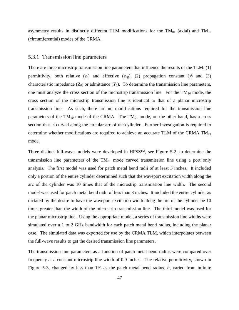
5.3.1 Transmission line parameters
There are three microstrip transmission line parameters that influence the results of the TLM: (1)
permittivity, both relative (εr) and effective (εeff), (2) propagation constant (γ) and (3)
characteristic impedance (Z0) or admittance (Y0). To determine the transmission line parameters,
one must analyze the cross section of the microstrip transmission line. For the TM10 mode, the
cross section of the microstrip transmission line is identical to that of a planar microstrip
transmission line. As such, there are no modifications required for the transmission line
parameters of the TM10 mode of the CRMA. The TM01 mode, on the other hand, has a cross
section that is curved along the circular arc of the cylinder. Further investigation is required to
determine whether modifications are required to achieve an accurate TLM of the CRMA TM01
mode.
Three distinct full-wave models were developed in HFSS, see Figure 5-2, to determine the
transmission line parameters of the TM01 mode curved transmission line using a port only
analysis. The first model was used for patch metal bend radii of at least 3 inches. It included
only a portion of the entire cylinder determined such that the waveport excitation width along the
arc of the cylinder was 10 times that of the microstrip transmission line width. The second
model was used for patch metal bend radii of less than 3 inches. It included the entire cylinder as
dictated by the desire to have the waveport excitation width along the arc of the cylinder be 10
times greater than the width of the microstrip transmission line. The third model was used for
the planar microstrip line. Using the appropriate model, a series of transmission line widths were
simulated over a 1 to 2 GHz bandwidth for each patch metal bend radius, including the planar
case. The simulated data was exported for use by the CRMA TLM, which interpolates between
the full-wave results to get the desired transmission line parameters.
The transmission line parameters as a function of patch metal bend radius were compared over
frequency at a constant microstrip line width of 0.9 inches. The relative permittivity, shown in
Figure 5-3, changed by less than 1% as the patch metal bend radius, b, varied from infinite

48
(planar) down to 1.075” (~0.15λo). The propagation constant consists of a real part, the
attenuation constant (α), and an imaginary part, the phase constant (β). Both the attenuation
constant and phase constant exhibited no measurable change as a function of patch metal bend
radius as seen in Figure 5-4. The characteristic impedance, shown in Figure 5-5, exhibited the
largest change as a function of patch metal bend radius, increasing 7-10% as the patch metal
bend radius decreased.
Figure 5-2: HFSS models for the TM01 mode curved transmission line

49
Figure 5-3: CRMA TM01 mode microstrip transmission line relative permittivity
Figure 5-4: CRMA TM01 mode microstrip transmission line propagation constant
Figure 5-5: CRMA TM01 mode microstrip transmission line characteristic impedance
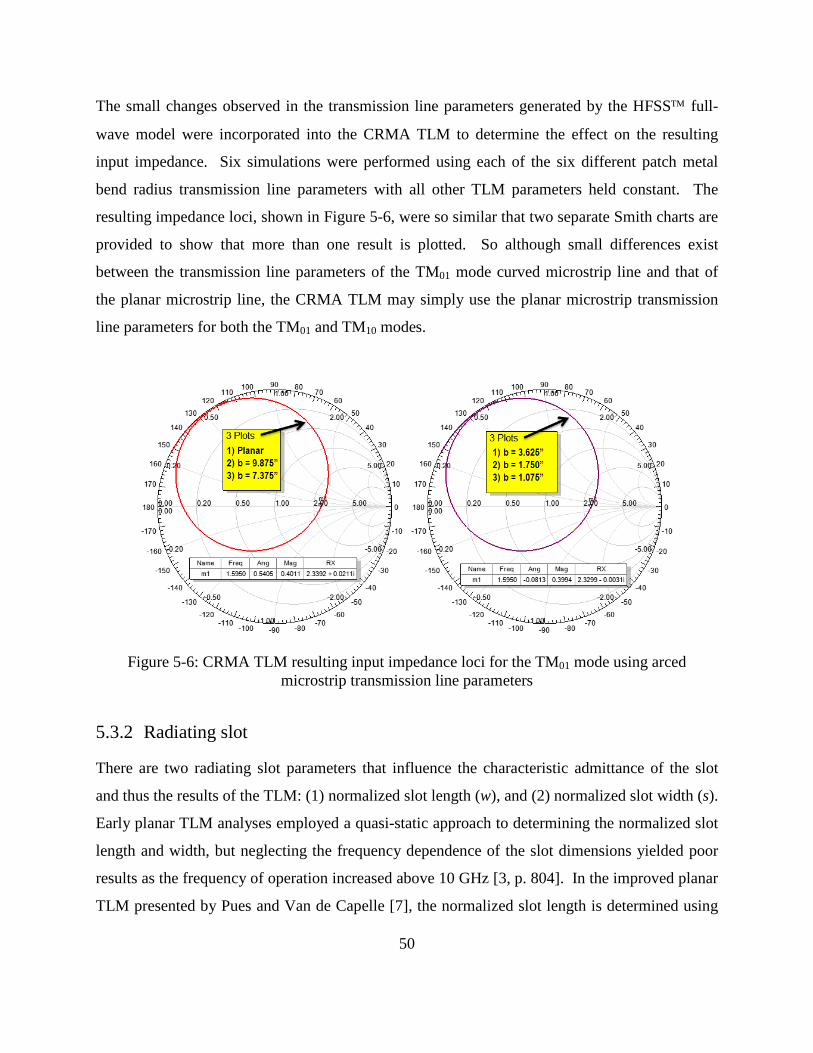
50
The small changes observed in the transmission line parameters generated by the HFSS full-
wave model were incorporated into the CRMA TLM to determine the effect on the resulting
input impedance. Six simulations were performed using each of the six different patch metal
bend radius transmission line parameters with all other TLM parameters held constant. The
resulting impedance loci, shown in Figure 5-6, were so similar that two separate Smith charts are
provided to show that more than one result is plotted. So although small differences exist
between the transmission line parameters of the TM01 mode curved microstrip line and that of
the planar microstrip line, the CRMA TLM may simply use the planar microstrip transmission
line parameters for both the TM01 and TM10 modes.
Figure 5-6: CRMA TLM resulting input impedance loci for the TM01 mode using arced
microstrip transmission line parameters
5.3.2 Radiating slot
There are two radiating slot parameters that influence the characteristic admittance of the slot
and thus the results of the TLM: (1) normalized slot length (w), and (2) normalized slot width (s).
Early planar TLM analyses employed a quasi-static approach to determining the normalized slot
length and width, but neglecting the frequency dependence of the slot dimensions yielded poor
results as the frequency of operation increased above 10 GHz [3, p. 804]. In the improved planar
TLM presented by Pues and Van de Capelle [7], the normalized slot length is determined using

51
the planar waveguide model of a microstrip line. In the planar waveguide model, the microstrip
line is modeled as a parallel plate waveguide of finite plate width equal to the effective width of
the microstrip line, with perfect magnetic conductors on the side walls and perfect electric
conductors on the top and bottom walls. The normalized slot width is derived empirically by
curve fitting numerical results from full-wave analyses. In this section, we propose
modifications to these slot parameters to account for the effect of the patch metal bend radius on
the CRMA TM01 (axial) and TM10 (circumferential) modes.
As we attempt to make changes to the normalized slot length and width to account for the effects
of the patch metal bend radius, we recall the impact of the slot dimensions on the planar
microstrip antenna in Section 5.2. For the planar microstrip antenna, increases to the normalized
slot length had the effect of decreasing or tightening the impedance locus circle, while increases
in the normalized slot width had the effect of lowering the resonant frequency. Scaling the
normalized slot width and length, therefore, provides a means to tune the TLM to match the
results from the CRMA full-wave 3D analysis.
5.3.2.1 Derivation of slot scale factors A Smith chart comparing the TLM results to those of HFSS for the TM01 mode of the CRMA
with a patch metal bend radius of 1.075 inch is given in Figure 5-7. The impedance locus of the
planar TLM without any slot modifications exhibited a larger diameter with a higher resonant
frequency. In order to better match the TLM impedance locus to that of HFSS, the normalized
slot width and length were increased by factors of 1.325 and 1.83, respectively. The resulting
impedance locus agreed very well with the HFSS result in diameter, VSWR 2:1 bandwidth and
resonant frequency as seen in Figure 5-7.

52
Figure 5-7: Smith chart analysis of the radiating slot modifications to the CRMA TLM for the
TM01 mode with a patch metal bend radius, b, of 1.075 inch
A Smith chart comparing the TLM results to those of HFSS for the TM10 mode of the CRMA
with a patch metal bend radius of 1.075 inch is given in Figure 5-8. The impedance locus of the
planar TLM without any slot modifications had a similar diameter to that of the HFSS results.
However, the resonant frequency predicted by the planar TLM was appreciably lower than that
obtained in HFSS. In order to better match the TLM impedance locus to that of HFSS, the
normalized slot width and length were changed by factors of 0.81 and 1.02, respectively. The
resulting impedance locus agreed very well with the HFSS result in diameter, VSWR 2:1
bandwidth and resonant frequency as seen in Figure 5-8.

53
Figure 5-8: Smith chart analysis of the radiating slot modifications to the CRMA TLM for the
TM10 mode with a patch metal bend radius, b, of 1.075 inch
Results similar to those shown in Figure 5-7 and Figure 5-8 were obtained for each different
patch metal bend radius analyzed in Chapter 4 for the single CRMA and two CB-CRMA full-
wave models. The resulting slot width and length scale factor values obtained for each of the
three models were normalized to the scale factor values obtained for the planar embodiment of
the respective model. These normalized values are plotted as a function of the inverse of the
patch metal bend radius for the TM01 and TM10 modes in Figure 5-9 and Figure 5-10,
respectively. The inverse of the patch metal bend radius is used to accommodate the planar
microstrip antenna, whose inverse patch metal bend radius is zero.

54
For the CRMA TM01 mode, the normalized slot width scale factor exhibits little to no change as
a function of patch metal bend radius, whereas the normalized slot length scale factor exhibits a
substantial increase as the patch metal bend radius is decreased. Increasing the length of the slot
yields a tighter impedance locus circle. This effectively models the increased impedance
bandwidth seen in the CRMA full-wave 3D analysis (see Figure 4-9, Figure 4-14 and Figure
4-19). Curve fitting the data in Figure 5-9 provides the following equations for slot scale factors.
𝑇𝑀01𝑠𝑠𝑐𝑎𝑙𝑒 = 0.0098𝑏
+ 1 (5.5)
𝑇𝑀01𝑤𝑠𝑐𝑎𝑙𝑒 = 0.0936𝑏
+ 1 (5.6)
where b is the radius of curvature of the patch metal in wavelengths per Figure 3-1 and
TM01sscale and TM01wscale are the resulting slot width and length scale factors, respectively.
Note that the scale factors are normalized to the actual slot scale factors required to achieve an
accurate TLM for a planar embodiment of the microstrip antenna. Hence, as the patch metal
bend radius, b, goes to infinity, both scale factors equal one. Also, the curvature of the patch
metal is given in wavelengths to make the computation of the scale factors independent of
operating frequency.
Figure 5-9: TM01 CRMA TLM slot width and length scale factors vs. inverse patch bend radius
y = 0.0098x + 1 R² = 0.9859
y = 0.0936x + 1 R² = 0.9899
0.80.9
11.11.21.31.41.51.61.71.8
0 2 4 6 8
Slot
Sca
le F
acto
r
Inverse Patch Radius (1/b) [wavelengths]
Slot Width TM01
Slot Length TM01
Decreasing Patch Radius

55
The normalized slot width and length scale factors of the TM10 mode decrease as the patch metal
bend radius is decreased. Curve fitting the data in Figure 5-9 provides the following equations
for slot scale factors.
𝑇𝑀10𝑠𝑠𝑐𝑎𝑙𝑒 = −0.0482𝑏
+ 1 (5.7)
𝑇𝑀10𝑤𝑠𝑐𝑎𝑙𝑒 = −0.0114𝑏
+ 1 (5.8)
where b is the radius of curvature of the patch metal in wavelengths per Figure 3-1 and
TM10sscale and TM10wscale are the resulting slot width and length scale factors, respectively.
Note that the scale factors are normalized to the actual slot scale factors required to achieve an
accurate TLM for a planar embodiment of the microstrip antenna. Hence, as the patch metal
bend radius, b, goes to infinity, both scale factors equal one. Also, the curvature of the patch
metal is given in wavelengths to make the computation of the scale factors independent of
operating frequency.
Figure 5-10: TM10 CRMA TLM slot width and length scale factors vs. inverse patch radius
y = -0.0482x + 1 R² = 0.9789
y = -0.0114x + 1 R² = 0.6898
0
0.2
0.4
0.6
0.8
1
1.2
0 2 4 6 8
Slot
Sca
le F
acto
r
Inverse Patch Radius (1/b) [wavelengths]
Slot Width TM10
Slot Length TM10
Decreasing Patch Radius

56
The significant decrease in the TM10 mode slot width scale factor accounts for the resonant
frequency increase seen in the HFSS CRMA study (see Figure 4-8, Figure 4-13 and Figure
4-18). Intuitively, it makes sense that the slot width of the TM10 mode decreases as the patch
bend radius decreases because the fringing fields couple harder to the portion of the ground
closest to the radiating edge. For patches conformed to a cylinder, like the CRMA, the distance
between the radiating edge patch metal and the ground increases at a rate inversely proportional
to the cylinder radius as you move along the circumference away from the patch metal edge.
Thus, the fringing fields do not couple out as far, making the effective slot width smaller. To
prove this point, an analysis was performed on a planar patch where the ground and substrate
were bent away from the patch metal at angles of 0°, 15°, and 30° as shown in Figure 5-11. The
probe excitation location was adjusted appropriately to achieve 50Ω resonance for each bend
angle of the ground and substrate. The resulting input return loss in Figure 5-11 clearly shows
that the resonance frequency increased as the ground and substrate bend angle increased
supporting the slot width scale factor change required as a function of patch metal bend radius
for the TM10 mode of the CRMA.
Figure 5-11: Physical explanation of TM10 mode radiating slot width scale factor
5.4 Resulting CRMA TLM
A Matlab code implementation of the resulting CRMA TLM can be found in Appendix A.1 and
Appendix A.2.

57
The physical depiction of the CRMA from Figure 3-1 is repeated here in Figure 5-12 for
convenience in relating structural parameters to the newly developed CRMA TLM.
Figure 5-12: Cylindrical rectangular microstrip antenna (CRMA)
The CRMA TLM is schematically depicted in Figure 5-13. This model is identical to that of the
planar TLM depicted in Figure 2-2 as the CRMA TLM is directly derived from the transmission
line model first proposed by Munson [1] and later improved by Derneryd [6] and Pues and Van
de Capelle [7]. The only difference between the CRMA TLM and the planar TLM is in the
computation of the radiating slot self-admittance, Ys, and mutual admittance, Ym. Like the planar
TLM, its usefulness is limited to rectangular or square patches, but extensions to other shapes are
possible.

58
Figure 5-13: CRMA three-port transmission line model
As was the case with the planar TLM, the CRMA TLM only considers the fundamental mode of
the antenna. This can be an issue for electrically large patches or patches with parasitic shorting
pins or slots. Consequently, we have to be aware of this limitation when utilizing the CRMA
TLM.
5.4.1 Radiating slot admittance
The admittance of the radiating slot consists of a self-admittance, Ys, in parallel with a mutual
admittance, Ym. The total slot admittance is equal to Ys + Ym.
To calculate the radiating slot self-admittance, Ys, it is broken down into its real, self-
conductance (Gs), and imaginary, self-susceptance (Bs), parts with [4]
( )tan Ss cB Y β= (5.9)
( )2 2
2 3
1 sin 1 cos sin cos 2 124 12 3s
w s s w wG w Si w ww w wπη
≈ + + − × − + + − (5.10)
where Yc is the characteristic admittance, β is the propagation constant of the microstrip line, S is
the open-end microstrip line extension, η is the free space impedance, w is the normalized slot
length (koWe), s is the normalized slot width (koS), ko is the free space wave number, and
0
sin( )x uSi x du
u= ∫ .
Computation of the radiating slot effective width, S, for the CRMA TLM is given by

59
𝑆 = 𝑆1(𝑇𝑀01𝑠𝑠𝑐𝑎𝑙𝑒), for CRMA 𝑇𝑀01 mode
𝑆1(𝑇𝑀10𝑠𝑠𝑐𝑎𝑙𝑒), for CRMA 𝑇𝑀10 mode (5.11)
𝑇𝑀01𝑠𝑠𝑐𝑎𝑙𝑒 = 0.0098𝑏
+ 1 (5.12)
𝑇𝑀10𝑠𝑠𝑐𝑎𝑙𝑒 = −0.0482𝑏
+ 1 (5.13)
𝑆1 = ℎΨ1Ψ3Ψ5Ψ4
(5.14)
Ψ1 = 0.434907 𝜀1𝑒𝑓𝑓0.81 +0.26
𝜀1𝑒𝑓𝑓0.81 −0.189
𝑥0.8544+0.236𝑥0.8544+0.87
(5.15)
Ψ2 = 1 + 𝑥0.371
2.358𝜀𝑟1+1 (5.16)
Ψ3 = 1 + 0.5274 tan−10.084𝑥
1.9413Ψ2
𝜀1𝑒𝑓𝑓0.9236 (5.17)
Ψ4 = 1 + 0.0377 tan−1(0.067𝑥1.456) 6 − 5𝑒0.036(1−𝜀𝑟1) (5.18)
Ψ5 = 1 − 0.218𝑒(−7.5𝑥) (5.19)
𝑥 = 2𝑊
ℎ , for CRMA 𝑇𝑀01 mode2𝐿
ℎ , for CRMA 𝑇𝑀10 mode (5.20)
where, per Figure 5-12, b is the patch metal bend radius in wavelengths, 2W and 2L are the patch
metal width and length in meters, h is the patch substrate height in meters, 𝜀𝑟1 is the relative
permittivity of the patch substrate, and 𝜀1𝑒𝑓𝑓 is the effective permittivity of the microstrip
transmission line substrate. Note that the only difference between the planar TLM derivation of
the radiating slot effective width, S, in [4] and that of the CRMA TLM above is the addition of
the 𝑇𝑀01𝑠𝑠𝑐𝑎𝑙𝑒 and 𝑇𝑀10𝑠𝑠𝑐𝑎𝑙𝑒 scale factors.
Computation of the radiating slot effective length, We, for the CRMA TLM is given by
𝑊𝑒 = 𝑊1(𝑇𝑀01𝑤𝑠𝑐𝑎𝑙𝑒), for CRMA 𝑇𝑀01 mode𝑊1(𝑇𝑀10𝑤𝑠𝑐𝑎𝑙𝑒), for CRMA 𝑇𝑀10 mode (5.21)
𝑇𝑀01𝑤𝑠𝑐𝑎𝑙𝑒 = 0.0936𝑏
+ 1 (5.22)
𝑇𝑀10𝑤𝑠𝑐𝑎𝑙𝑒 = −0.0114𝑏
+ 1 (5.23)
𝑊1 = 𝑛3
+ (𝑅𝑤 + 𝑃𝑤)1 3 − (𝑅𝑤 − 𝑃𝑤)1 3 (5.24)

60
𝑅𝑤 = (𝑃𝑤2 + 𝑄𝑤3 ) (5.25)
𝑃𝑤 = 𝑛33
+ 𝑆𝑤2𝑊2 −
𝑛3 (5.26)
𝑄𝑤 = 𝑆𝑤3− 𝑛
32 (5.27)
𝑆𝑤 = 𝑐02
4𝑓2𝜀1𝑒𝑓𝑓−1 (5.28)
𝑊2 = 2𝜋ℎ
ln𝐹1𝐹2ℎ+1+2ℎ𝐹2
2
(5.29)
𝐹1 = 6 + (2𝜋 − 6)𝑒−4𝜋2
3 ℎ 𝐹2 34
(5.30)
𝐹2 = 𝑝 + 𝑡𝑚𝜋
⎝
⎜⎜⎜⎛
1 + ln
⎝
⎜⎜⎛
4
𝑡𝑚ℎ 2+ 1
𝜋𝑝 𝑡𝑚 +1.12
⎠
⎟⎟⎞
⎠
⎟⎟⎟⎞
(5.31)
𝑛 = 2𝐿, for CRMA 𝑇𝑀01 mode2𝑊, for CRMA 𝑇𝑀10 mode (5.32)
𝑝 = 2𝑊, for CRMA 𝑇𝑀01 mode2𝐿, for CRMA 𝑇𝑀10 mode (5.33)
where, per Figure 5-12, b is the patch metal bend radius in wavelengths, 2W and 2L are the patch
metal width and length in meters, h is the patch substrate height in meters, 𝑡𝑚 is the patch metal
thickness, 𝜀1𝑒𝑓𝑓 is the effective permittivity of the microstrip transmission line substrate, 𝑐0 is the
speed of light in free space and f is the operating frequency. Note that the only difference
between the planar TLM derivation of the radiating slot effective length, We, in [4] and that of
the CRMA TLM above is the addition of the 𝑇𝑀01𝑤𝑠𝑐𝑎𝑙𝑒 and 𝑇𝑀10𝑤𝑠𝑐𝑎𝑙𝑒 scale factors.
Multiplying the above self-admittance values by auxiliary coupling functions gives the mutual
admittance of the radiating slots [4]. As with the planar TLM, the mutual admittance accounts
for the coupling between the two radiating edge slots, as well as the impact of the two non-
radiating edge slots.
𝐺𝑚 = 𝐺𝑠𝐹𝑔𝐾𝑔 (5.34)
61
𝐵𝑚 = 𝐵𝑠𝐹𝑏𝐾𝑏 (5.35)
The conductance, 𝐹𝑔𝐾𝑔, and susceptance, 𝐹𝑏𝐾𝑏, auxiliary coupling functions are given by [4]
( ) ( )2
0 2224gsF J l J l
s= +
− (5.36)
𝐾𝑔 = 1 (5.37)
( ) ( )2
0 22
2
2
242 3 12ln
2 2 24
b
e
sY l Y lsF
ss Cs
π +−=
+ − + −
(5.38)
𝐾𝑏 = 1 − 𝑒−0.21𝑤 (5.39)
where Jn and Yn are Bessel functions, l is the normalized center distance between slots
(ko(L1+L2+S)), s is the normalized slot width (koS), w is the normalized slot length (koWe), ko is
the free space wave number, and Ce is Euler’s constant (0.577216). For further explanation of
these variables, please see [4, pp. 527-578].
5.4.2 Transmission line parameters
There are three microstrip transmission line parameters that influence the results of the CRMA
TLM: (1) permittivity, both relative (εr) and effective (εeff), (2) propagation constant (γ) and (3)
characteristic impedance (Z0) or admittance (Y0). We know from the transmission line
investigation in Section 5.3.1 that both the TM01 and TM10 modes of the CRMA may use the
transmission line parameters derived for a planar microstrip transmission line having the same
construction as the CRMA. The planar transmission line parameters may be found using a
closed form solution or through computational analysis. For simple microstrip transmission lines
with a single substrate and no superstrate, it is easiest to use closed form expressions such as
those in [31]. The closed form solution is computationally more efficient and provides accurate
results over a wide range of line widths and frequencies. For more complicated microstrip
structures that have a superstrate, it may be more desirable to use a computational model such as
the port only analysis in Ansys HFSS. The computational model requires an initial set of runs

62
to simulate the transmission line over a finite number of widths and frequencies. That data is
then imported into the CRMA TLM and interpolated to find the transmission line parameters at
the desired line width and frequency. The initial computational simulations require additional
time to generate models and results, but the added accuracy, especially when using more
complex constructions with superstrates, may justify the added time.
5.4.3 Feed model
5.4.3.1 Probe A probe feed may be added to port 3 of the CRMA TLM in Figure 5-13. The probe feed is
modeled as a simple resistor and inductor in series. The resistance of the feed is determined
using the equation for a Hertzian monopole:
𝑅𝑟𝑎𝑑 = 10(𝑘 × ℎ)2 (5.40)
where k is the free space wave number and h is the height of the microstrip substrate. The
inductance of the feed is determined using the equation for the self-inductance of a straight round
wire at high frequency [30]:
𝐿 = 0.2ℎ ln 4.0ℎ𝑑 − 1.00 + 𝑑
2.0ℎ+ 𝜇𝑟𝑇(𝑥)
4.0 (𝜇𝐻) (5.41)
𝑇(𝑥) = 0.873011+0.00186128𝑥1.0−0.278381𝑥+0.127964𝑥2
(5.42)
𝑥 = 𝜋𝑑2.0𝜇𝑓𝜎
(5.43)
where h is the height of the microstrip substrate, d is the diameter of the probe, µr is the relative
permeability of the substrate, µ is the permeability of the substrate, σ is the conductance of the
probe metal, and f is the frequency of operation.
5.4.3.2 Microstrip line A microstrip line feed may be added to port 3 of the CRMA TLM in Figure 5-13. The microstrip
line feed is simply added as a transmission line of length equal to the length of the feed with

63
transmission line parameters equal to those of the feed line. Since we have already shown that
the transmission line parameters of the microstrip line are not affected by the radius of curvature
of the CRMA, we can simply use a planar microstrip line to derive the necessary parameters. An
example transmission line model for a microstrip line edge fed CRMA is shown in Figure 5-14.
This model assumes that microstrip line feed, highlighted on the left side of the model, consists
of two distinct microstrip lines each having its own unique width and length. Since the CRMA is
edge fed by the microstrip line, the admittance of one of the radiating slots, two in this case, is
located right at the microstrip line feed interface. The other radiating slot is on the opposite side
of the patch a distance of the full patch length for the TM01 mode or width for the TM10 mode
away.
Figure 5-14: Example microstrip line edge fed CRMA TLM
5.5 Summary Remarks
An accurate CRMA TLM was derived from the planar TLM by simply scaling the radiating slot
normalized width (s) and length (w) based on curve fitting the results from three separate full-
wave 3D Ansys HFSS models. The CRMA TLM, like the planar TLM, only considers the
fundamental mode. As such, the CRMA TLM has the same limitations as the planar TLM and
its accuracy will suffer for electrically large patches or patches with parasitic shorting pins or
slots that generate higher order modes. With these limitation in mind, the next step is to build
and measure a series of CRMA designs to verify the accuracy of the Ansys HFSS™ models, as
well as the newly developed CRMA TLM.

64
CHAPTER 6
CRMA MEASURED RESULTS
This chapter compares results derived using the full-wave Ansys HFSS models and the newly
developed CRMA TLM to a series of microstrip line fed CRMA designs that were built and
tested by Professor Ruyle and her team of graduate and undergraduate students at the University
of Oklahoma [29].
6.1 Fabricated CRMA Overview
The CRMA was fabricated on a 0.031 inch thick Rogers RO5880 PTFE substrate. The
fabricated CRMA was designed to be matched to 50Ω at approximately 5 GHz. The final design
dimensions, given in Figure 6-1, were used in the fabrication of each and every CRMA.
Figure 6-1: CRMA fabricated design dimensions
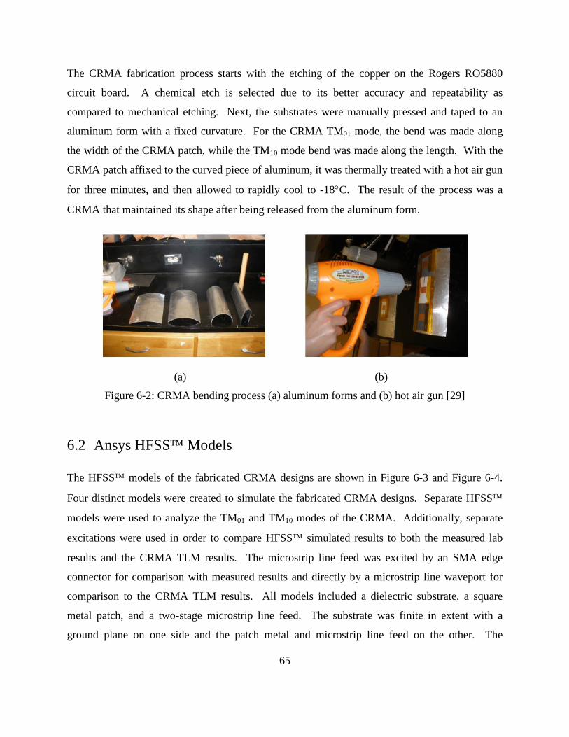
65
The CRMA fabrication process starts with the etching of the copper on the Rogers RO5880
circuit board. A chemical etch is selected due to its better accuracy and repeatability as
compared to mechanical etching. Next, the substrates were manually pressed and taped to an
aluminum form with a fixed curvature. For the CRMA TM01 mode, the bend was made along
the width of the CRMA patch, while the TM10 mode bend was made along the length. With the
CRMA patch affixed to the curved piece of aluminum, it was thermally treated with a hot air gun
for three minutes, and then allowed to rapidly cool to -18°C. The result of the process was a
CRMA that maintained its shape after being released from the aluminum form.
(a) (b)
Figure 6-2: CRMA bending process (a) aluminum forms and (b) hot air gun [29]
6.2 Ansys HFSS Models
The HFSS models of the fabricated CRMA designs are shown in Figure 6-3 and Figure 6-4.
Four distinct models were created to simulate the fabricated CRMA designs. Separate HFSS
models were used to analyze the TM01 and TM10 modes of the CRMA. Additionally, separate
excitations were used in order to compare HFSS simulated results to both the measured lab
results and the CRMA TLM results. The microstrip line feed was excited by an SMA edge
connector for comparison with measured results and directly by a microstrip line waveport for
comparison to the CRMA TLM results. All models included a dielectric substrate, a square
metal patch, and a two-stage microstrip line feed. The substrate was finite in extent with a
ground plane on one side and the patch metal and microstrip line feed on the other. The

66
substrate was modelled with dielectric loss. All printed metal was modeled using copper
boundary conditions on infinitely thin sheets. A vacuum filled box surrounds the entire
structure, and PML (perfectly matched layer) boundaries are employed on the walls of the
vacuum filled box for accuracy.
Figure 6-3: HFSS CRMA model for comparison with measurements
Figure 6-4: HFSS CRMA model for comparison with CRMA TLM
6.3 CRMA TLM
The CRMA TLM in Figure 6-5 accounts for all aspects of the fabricated CRMA except for the
edge mount SMA to microstrip connector. As such, the results of the CRMA TLM cannot be

67
directly compared to the measured results. Instead, the CRMA TLM will be validated by
comparing its results to those of the HFSS CRMA models in Figure 6-4. These HFSS models
are identical to the HFSS CRMA models in Figure 6-3 minus the SMA to microstrip
connector. Thus the validity of the HFSS CRMA models in Figure 6-4 is established through
comparison of the results of the HFSS CRMA models in Figure 6-3 with measured results.
Figure 6-5: Fabricated CRMA TLM
6.4 Ansys HFSS Comparison to Measured Results
The Ansys HFSS models in Figure 6-3 were simulated for each of the fabricated CRMA bend
radii: planar, 15.0 cm, 9.208 cm, 4.469 cm, and 1.25 cm. The results of the simulations
compared very favorably to the measured results of the fabricated CRMA, confirming the
validity of the HFSS models. The worst case error in center operating frequency between the
HFSS and measured results was less than 3% as seen in Figure 6-6 to Figure 6-14, while the
difference in VSWR 2:1 fractional bandwidth was less than 0.25%.

68
Figure 6-6: Fabricated planar microstrip – HFSS vs. measured results
Figure 6-7: Fabricated 15.0 cm TM01 CRMA – HFSS vs. measured results

69
Figure 6-8: Fabricated 9.208 cm TM01 CRMA – HFSS vs. measured results
Figure 6-9: Fabricated 4.469 cm TM01 CRMA – HFSS vs. measured results

70
Figure 6-10: Fabricated 1.25 cm TM01 CRMA – HFSS vs. measured results
Figure 6-11: Fabricated 15.0 cm TM10 CRMA – HFSS vs. measured results

71
Figure 6-12: Fabricated 9.208 cm TM10 CRMA – HFSS vs. measured results
Figure 6-13: Fabricated 4.469 cm TM10 CRMA – HFSS vs. measured results
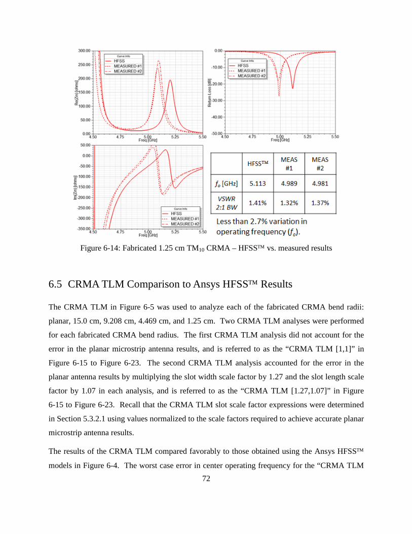
72
Figure 6-14: Fabricated 1.25 cm TM10 CRMA – HFSS vs. measured results
6.5 CRMA TLM Comparison to Ansys HFSS Results
The CRMA TLM in Figure 6-5 was used to analyze each of the fabricated CRMA bend radii:
planar, 15.0 cm, 9.208 cm, 4.469 cm, and 1.25 cm. Two CRMA TLM analyses were performed
for each fabricated CRMA bend radius. The first CRMA TLM analysis did not account for the
error in the planar microstrip antenna results, and is referred to as the “CRMA TLM [1,1]” in
Figure 6-15 to Figure 6-23. The second CRMA TLM analysis accounted for the error in the
planar antenna results by multiplying the slot width scale factor by 1.27 and the slot length scale
factor by 1.07 in each analysis, and is referred to as the “CRMA TLM [1.27,1.07]” in Figure
6-15 to Figure 6-23. Recall that the CRMA TLM slot scale factor expressions were determined
in Section 5.3.2.1 using values normalized to the scale factors required to achieve accurate planar
microstrip antenna results.
The results of the CRMA TLM compared favorably to those obtained using the Ansys HFSS
models in Figure 6-4. The worst case error in center operating frequency for the “CRMA TLM

73
[1,1]” analysis was less than 1.4%, while the “CRMA TLM [1.29,1.07]” analysis was less than
0.9%. The worst case error in VSWR 2:1 fractional bandwidth for the “CRMA TLM [1,1]”
analysis was less than 0.22%, while the “CRMA TLM [1.29,1.07]” analysis was less than 0.18%.
These results suggest that going through the extra steps of calibrating the CRMA TLM slot scale
factors to a trusted planar microstrip antenna result is unnecessary.
Figure 6-15: Fabricated planar microstrip – CRMA TLM vs. HFSS results
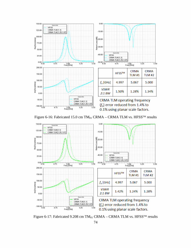
74
Figure 6-16: Fabricated 15.0 cm TM01 CRMA – CRMA TLM vs. HFSS results
Figure 6-17: Fabricated 9.208 cm TM01 CRMA – CRMA TLM vs. HFSS results

75
Figure 6-18: Fabricated 4.469 cm TM01 CRMA – CRMA TLM vs. HFSS results
Figure 6-19: Fabricated 1.25 cm TM01 CRMA – CRMA TLM vs. HFSS results
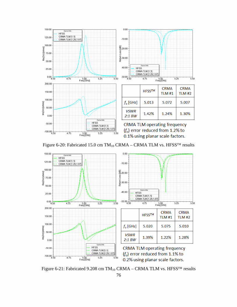
76
Figure 6-20: Fabricated 15.0 cm TM10 CRMA – CRMA TLM vs. HFSS results
Figure 6-21: Fabricated 9.208 cm TM10 CRMA – CRMA TLM vs. HFSS results

77
Figure 6-22: Fabricated 4.469 cm TM10 CRMA – CRMA TLM vs. HFSS results
Figure 6-23: Fabricated 1.25 cm TM10 CRMA – CRMA TLM vs. HFSS results
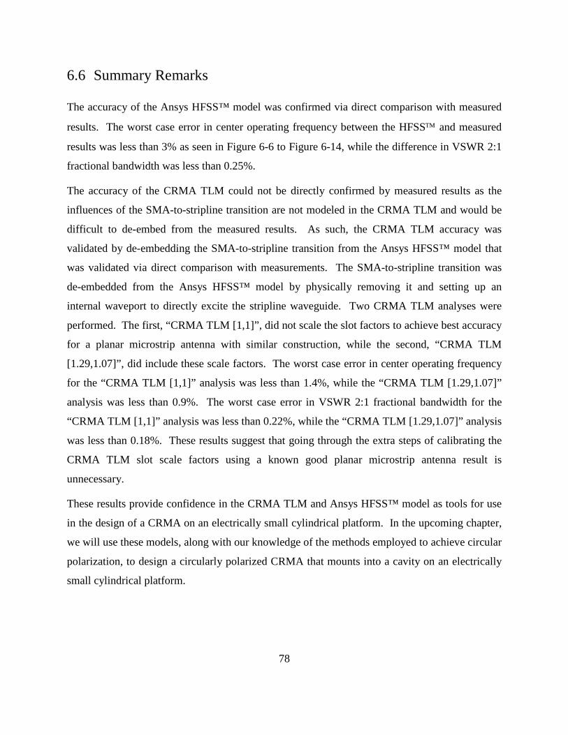
78
6.6 Summary Remarks
The accuracy of the Ansys HFSS™ model was confirmed via direct comparison with measured
results. The worst case error in center operating frequency between the HFSS and measured
results was less than 3% as seen in Figure 6-6 to Figure 6-14, while the difference in VSWR 2:1
fractional bandwidth was less than 0.25%.
The accuracy of the CRMA TLM could not be directly confirmed by measured results as the
influences of the SMA-to-stripline transition are not modeled in the CRMA TLM and would be
difficult to de-embed from the measured results. As such, the CRMA TLM accuracy was
validated by de-embedding the SMA-to-stripline transition from the Ansys HFSS™ model that
was validated via direct comparison with measurements. The SMA-to-stripline transition was
de-embedded from the Ansys HFSS™ model by physically removing it and setting up an
internal waveport to directly excite the stripline waveguide. Two CRMA TLM analyses were
performed. The first, “CRMA TLM [1,1]”, did not scale the slot factors to achieve best accuracy
for a planar microstrip antenna with similar construction, while the second, “CRMA TLM
[1.29,1.07]”, did include these scale factors. The worst case error in center operating frequency
for the “CRMA TLM [1,1]” analysis was less than 1.4%, while the “CRMA TLM [1.29,1.07]”
analysis was less than 0.9%. The worst case error in VSWR 2:1 fractional bandwidth for the
“CRMA TLM [1,1]” analysis was less than 0.22%, while the “CRMA TLM [1.29,1.07]” analysis
was less than 0.18%. These results suggest that going through the extra steps of calibrating the
CRMA TLM slot scale factors using a known good planar microstrip antenna result is
unnecessary.
These results provide confidence in the CRMA TLM and Ansys HFSS™ model as tools for use
in the design of a CRMA on an electrically small cylindrical platform. In the upcoming chapter,
we will use these models, along with our knowledge of the methods employed to achieve circular
polarization, to design a circularly polarized CRMA that mounts into a cavity on an electrically
small cylindrical platform.

79
CHAPTER 7
DESIGN OF A CIRCULARLY POLARIZED
CRMA
Having verified the accuracy of the Ansys HFSS™ full-wave model and the CRMA TLM
against measured data, we will now use these models to design a circularly polarized CRMA.
We start the design process in Section 7.1 with an overview of the application, which is a
precision guided munition. In Section 7.2, we discuss the design requirements. In Section 7.3,
we provide an overview of the design approach for meeting the requirements. Section 7.4 begins
the actual design using the CRMA TLM to make design trades with respect to material set and
dielectric stack-up. We also use the CRMA TLM to determine the initial patch metal dimensions
and feed locations. In Section 7.5, we use Ansys HFSS™ to fine tune the dimensions of the
patch and feed locations. We also design and integrate a conformal stripline quadrature hybrid
circuit with the CRMA to generate the desired circular polarization. In Section 0, we present and
discuss the compliance of the circularly polarized CRMA design with the application
requirements. We conclude with summary remarks in Section 7.7.
7.1 Application Overview
The United States government recently funded the development of a Precision Guidance Kit
(PGK) for the M107, M795 and M549/A1 155 mm artillery rounds that uses the Global
Positioning System (GPS) to guide the munition to its target. A PGK equipped 155 mm artillery
round is capable of hitting within a circular error probable (CEP) of less than 50 meters out to a
30 km range [32]. A non-guided 155 mm artillery round is only capable of hitting within a CEP
of 94-267 meters depending on the range out to 30 km [32]. The increased accuracy afforded by
PGK saves money by significantly reducing the number of shots and amount of collateral

80
damage. An example 155 mm artillery round is shown in Figure 7-1. The fuze of the munition
houses all PGK electronics, including the antenna.
Figure 7-1: Example 155 mm artillery round
7.2 Design Requirements
The PGK antenna must fit within the conformal cavity outlined in Figure 7-2, and receive the
right-hand circularly polarized (RHCP) GPS signal with enough gain to allow the receiver to
acquire and track GPS satellites. When specifying the necessary gain of the antenna, it is
important to understand the operation of the munition and GPS receiver. The 155 mm artillery
round is fired from a rifled barrel with a spin rate of up to 300 Hz. The spin rate decreases
throughout the flight, but is typically greater than 100 Hz. The GPS receiver integrates signal
power over the symbol period, which is 20 ms for GPS. This equates to a symbol rate of 50 Hz,
which means that the 155 mm artillery round goes through multiple rotations during the
integration of the signal power in a single GPS symbol. Therefore, as far as the GPS receiver is
concerned, the effective gain of the antenna is the average integrated gain over 360° of rotation.
Given this fact, it is convenient to define the antenna coordinate system in terms of a roll and
incidence angle as shown in Figure 7-3 and Figure 7-4. The integrated gain (IG) of the antenna
is given by
𝐼𝐺(𝛼,𝑓) = 20 log 1360 ∫ ℎ(𝛼,𝛽,𝑓)𝑑𝛽360
0 (7.1)

81
where h is the complex voltage response of the antenna at frequency (f), and incidence (α) and
roll angle (β) as defined in Figure 7-3 and Figure 7-4.
Figure 7-2: Conformal antenna cavity for PGK antenna
Figure 7-3: Arrival incidence angle (α) is defined relative to the vehicle spin axis
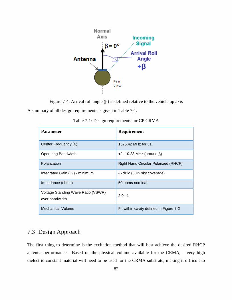
82
Figure 7-4: Arrival roll angle (β) is defined relative to the vehicle up axis
A summary of all design requirements is given in Table 7-1.
Table 7-1: Design requirements for CP CRMA
Parameter Requirement
Center Frequency (f0) 1575.42 MHz for L1
Operating Bandwidth +/ - 10.23 MHz (around f0)
Polarization Right Hand Circular Polarized (RHCP)
Integrated Gain (IG) - minimum -6 dBic (50% sky coverage)
Impedance (ohms) 50 ohms nominal
Voltage Standing Wave Ratio (VSWR)
over bandwidth 2.0 : 1
Mechanical Volume Fit within cavity defined in Figure 7-2
7.3 Design Approach
The first thing to determine is the excitation method that will best achieve the desired RHCP
antenna performance. Based on the physical volume available for the CRMA, a very high
dielectric constant material will need to be used for the CRMA substrate, making it difficult to

83
achieve wide impedance bandwidth performance. Also, the CRMA is cavity backed, and as
shown in Section 4.3.2.2, the impedance bandwidth of a cavity backed CRMA is roughly half
that of a CRMA with no cavity. Given the inherent impedance bandwidth challenges associated
with the physical space requirements of the CRMA, a dual probe excitation is chosen as it offers
wider bandwidth RHCP performance compared to the single probe excitation. The dual probe
excitation requires a feed network that produces two quadrature signals from a single input
signal. A stripline quadrature hybrid is selected as the feed network.
Now that the excitation method is selected, the design follows the procedure outlined below to
meet or exceed the requirements in Section 7.2.
1) Determine the dielectric stack-up of the CRMA.
The CRMA TLM is used to determine the dielectric materials. The lowest permittivity
CRMA substrate that is able to meet the requirements should be chosen in order to
achieve the largest input impedance bandwidth.
2) Determine the dimensions of the CRMA patch metal and probe feed excitation locations.
The CRMA TLM is used to determine the axial (TM01) and circumferential (TM10) extent
of the CRMA patch metal and the associated 50 Ω resonant feed locations.
3) Analyze and tune the CRMA TLM design in Ansys HFSS.
The Ansys HFSS model incorporates two stripline-to-via probe feeds excited by
independent stripline waveports with equal amplitude and approximately 90° of phase
difference in order to achieve circular polarization.
4) Design a conformal quadrature hybrid feed network.
A conformal stripline quadrature hybrid feed network is designed to excite the orthogonal
probe feeds of the CRMA with the appropriate phasing as determined in the analysis and
tuning of the stripline-to-via probe fed CRMA.
5) Integrate the conformal quadrature hybrid feed and CRMA in Ansys Designer.
Ansys Designer is used to connect the port S-parameters of the 3D full-wave HFSS
models for the stripline-to-via fed CRMA and the conformal stripline quadrature hybrid

84
feed network. Final adjustments are made to achieve the performance levels necessary to
meet the requirements in Table 7-1.
7.4 CRMA TLM Analysis
The CRMA TLM is used to determine the dielectric stack-up, patch metal dimensions and probe
feed locations, which constitutes the first two steps in the design approach outlined in Section
7.3.
The CRMA dielectric stack-up should be chosen to maximize impedance bandwidth
performance. Based on the mechanical volume requirements depicted in Figure 7-2, the entire
stack-up plus any connectors and cabling must be less than 0.45 inches thick. The dielectric
stack-up must include a protective superstrate or radome, the CRMA substrate, and the stripline
substrate. In order to maximize the impedance bandwidth performance, the CRMA substrate
height must be maximized, while the dielectric constant should be minimized. The dielectric
constant of the CRMA substrate is determined from the substrate height and maximum patch
metal area. The available patch metal area in the requirements is limited to 1.5 inches along the
length or spin axis of the munition. Allowing 0.25 inches around the perimeter of the CRMA for
mounting provisions, the total maximum patch axial length is one inch. The circumferential
length of the patch may be longer as it is allowed to wrap around the cylindrical mounting
structure. This fact helps in minimizing the dielectric constant of the patch substrate as the
circumferential or TM10 mode of the CRMA requires a longer patch length to achieve the same
operating frequency as the axial or TM01 mode.
Given the dimensional constraints, the CRMA TLM was used to determine the CRMA substrate
thickness and dielectric constant, as well as the initial patch metal dimensions and probe feed
locations. An analysis of the TM01 (axial) mode of the CRMA resulted in the selection of the
dielectric stack-up shown in Figure 7-5. This dielectric stack-up reserves 0.138 inches of
thickness for the RF connector and cabling, as well as any mechanical tolerances. Given the
dielectric stack-up in Figure 7-5, the CRMA TLM predicted a TM01 mode VSWR 2:1 impedance
bandwidth of 36 MHz (2.3%) about a center frequency of 1576 MHz as shown in Figure 7-6. An

85
analysis of the TM10 (circumferential) mode of the CRMA yielded a VSWR 2:1 impedance
bandwidth of 12 MHz (0.8%) about a center frequency of 1578 MHz as shown in Figure 7-6.
The CRMA TLM patch metal dimensions and feed excitation locations are also given in Figure
7-6. These dimensions will be used as a starting point for the full-wave HFSS analysis to
follow.
Figure 7-5: CRMA dielectric stack-up
Figure 7-6: CRMA TLM analysis results and initial design

86
7.5 Ansys HFSS Full-Wave Analysis
The full-wave HFSS analysis is used to analyze and tune the CRMA TLM design as well as
design a quadrature hybrid stripline feed circuit. The CRMA and the stripline quadrature feed
are then integrated together in Ansys Designer using the port S-parameters of the individual
full-wave HFSS models. This analysis constitutes the final three steps in the design approach
outlined in Section 7.3.
7.5.1 Analyze and tune CRMA TLM design
In order to achieve accurate radiation pattern results from the HFSS model, it is necessary to
model portions of the 155 mm munition with the CRMA as shown in Figure 7-7. The entire
modeled structure is enclosed within a vacuum filled box with PML (Perfectly Matched Layer)
boundaries defined on all six of its faces. A more detailed view of the CRMA is provided in
Figure 7-8. The CRMA consists of the dielectric stack-up in Figure 7-5, a rectangular metal
patch, and two orthogonal stripline-to-via probe feeds excited by stripline waveports.
Figure 7-7: Ansys HFSS CRMA model on 155 mm munition

87
Figure 7-8: Ansys HFSS CRMA model detail
Using the CRMA TLM design parameters given in Figure 7-6 as a starting point, the HFSS
CRMA model was used to tune the design for RHCP operation. The final CRMA design and
accompanying passive S-parameters are given in Figure 7-9. The VSWR 2:1 impedance
bandwidth performance was very similar to that predicted by the CRMA TLM. The TM01 (axial)
mode of the HFSS CRMA yielded a VSWR 2:1 impedance bandwidth of 30 MHz (1.9%)
about a center frequency of 1575 MHz, while the TM10 (circumferential) mode VSWR 2:1
impedance bandwidth was substantially smaller at 8 MHz (0.5%) about a center frequency of
1575 MHz. The final HFSS CRMA patch metal dimensions were nearly identical to that of
the CRMA TLM design with a maximum difference of 1.8%. The probe excitation locations, on
the other hand, differed by about 25%.
The large difference in probe excitation location between the CRMA TLM and HFSS™ model
may be attributed to errors in the underlying planar TLM. Recall from the derivation of the
CRMA TLM radiating slot scale factors in Section 5.3.2 that the slot length and width scale
factors were normalized to the values obtained for the planar model. The analysis of a cavity
backed planar microstrip antenna with the same dielectric stack-up yielded slot width and length
normalization factors of 1.0 and 0.85 respectively. Using these planar normalization factors, the
CRMA TLM yielded similar small patch size errors, but roughly half the probe excitation
location error compared to that obtained without normalization. The issue is the time and
resources spent determining the planar microstrip normalization factors. As such, the
recommended design approach is to set these normalization factors to 1.0 to generate the initial
CRMA TLM design and tune the conformal design in HFSS™.
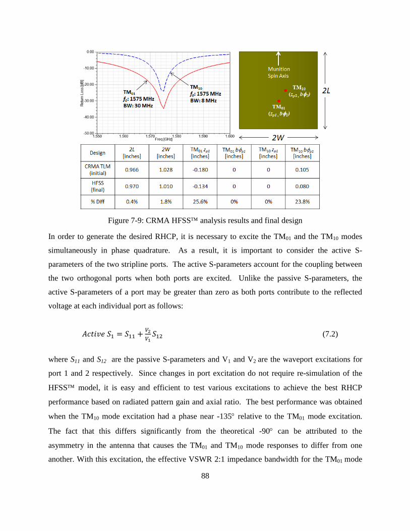
88
Figure 7-9: CRMA HFSS analysis results and final design
In order to generate the desired RHCP, it is necessary to excite the TM01 and the TM10 modes
simultaneously in phase quadrature. As a result, it is important to consider the active S-
parameters of the two stripline ports. The active S-parameters account for the coupling between
the two orthogonal ports when both ports are excited. Unlike the passive S-parameters, the
active S-parameters of a port may be greater than zero as both ports contribute to the reflected
voltage at each individual port as follows:
𝐴𝑐𝑡𝑖𝑣𝑒 𝑆1 = 𝑆11 + 𝑉2𝑉1𝑆12 (7.2)
where S11 and S12 are the passive S-parameters and V1 and V2 are the waveport excitations for
port 1 and 2 respectively. Since changes in port excitation do not require re-simulation of the
HFSS model, it is easy and efficient to test various excitations to achieve the best RHCP
performance based on radiated pattern gain and axial ratio. The best performance was obtained
when the TM10 mode excitation had a phase near -135° relative to the TM01 mode excitation.
The fact that this differs significantly from the theoretical -90° can be attributed to the
asymmetry in the antenna that causes the TM01 and TM10 mode responses to differ from one
another. With this excitation, the effective VSWR 2:1 impedance bandwidth for the TM01 mode

89
was 38 MHz (2.4%) about a center operating frequency of 1576 MHz as shown in Figure 7-10.
The TM10 mode had a significantly smaller VSWR 2:1 impedance bandwidth of 7 MHz (0.4%)
about a center operating frequency of 1573 MHz as shown in Figure 7-10. The peak RHCP
realized gain at 1575 MHz was 3.5 dBic with a minimum axial ratio of nearly 0.1 dB. A surface
plot of the 3D radiation pattern is provided in Figure 7-11. The radiation pattern is defined in the
munitions spin coordinate system per Figure 7-3 and Figure 7-4.
Figure 7-10: CRMA HFSS analysis active S-parameters
Figure 7-11: CRMA HFSS RHCP simulated 1575 MHz radiation pattern

90
The integrated gain (IG) of the final HFSS CRMA design was computed at 1565 MHz, 1575
MHz and 1585 MHz. A plot of the RHCP IG is given in Figure 7-12. The requirement for 50%
sky coverage with an IG of at least -6 dBic is met at 1565 MHz and 1575 MHz with coverage of
50% and 58% respectively. At 1585 MHz, the sky coverage with an IG of at least -6 dBic drops
below the requirement to a value of 34%.
Figure 7-12: CRMA HFSS simulated RHCP integrated gain
7.5.2 Design conformal quadrature hybrid feed network
A conformal quadrature hybrid feed network was designed in balanced stripline. Referring to
Figure 7-5, the stripline circuit resides between two 20 mil thick Rogers RO4232 substrates with
a dielectric constant of 3.2. The following procedure was followed in the design of the stripline
circuit.
1) Layout and analyze the quadrature hybrid in planar stripline.
Constructing and simulating a planar stripline circuit is far easier and more
computationally efficient than that of a conformal stripline circuit. Analytical
expressions for planar stripline are used to determine the line widths and lengths for 90

91
electrical degrees of 50 Ω and 35.4 Ω stripline for the quadrature hybrid circuit. Ansys
HFSS™ is used to analyze the planar layout.
Use of a planar stripline circuit is justified based on the fact that microstrip line
parameters do not vary significantly between planar and conformal constructions as
discovered in the development of the CRMA TLM in Section 5.3.1. Since stripline and
microstrip line are similar in construction, it is a fair extension to assume that a planar
stripline circuit will perform nearly the same as a conformal stripline circuit.
2) Conform the planar stripline circuit and analyze.
The planar stripline quadrature hybrid feed network is conformed to the surface of the
lower stripline substrate in HFSS™ using the “Wrap Sheet” function. A full-wave
HFSS™ analysis is performed on the conformed circuit and any necessary modifications
are made to achieve the desired performance.
The planar stripline quadrature hybrid feed layout is shown in Figure 7-13. The four ports of the
network are brought out to one inch long sections of coaxial waveguide with waveports defined
on each. Port 1 is the feed port for generating RHCP. Port 2 is the isolated port that will be
terminated in a matched 50 Ω load. In this design, that load is simply the coaxial waveport, but
in an actual design that load would be a small chip resistor or embedded resistive material such
as OmegaPly® or Ticer TCR®. Port 3 is the feed port of the TM01 axial mode. Port 4 is the
feed port of the TM10 circumferential mode. Note that the stripline circuit leading to Port 4 has
an extra length of transmission line in it. This is to generate the additional -45° necessary to
obtain the desired -135° difference in Port 4 relative to Port 3.

92
Figure 7-13: Planar stripline quadrature hybrid feed layout
The planar stripline quadrature hybrid feed analysis results, shown in Figure 7-14, yielded an
excellent return loss of less than -20 dB at Port 1 with more than -34 dB isolation to Port 2 over
the desired 1565 MHz to 1585 MHz band. The insertion loss to Port3 was -3.03 dB, while a
slightly higher insertion loss of -3.80 dB was observed to Port 4 due to the additional
transmission line length. The phase of Port 3 relative to Port 4 was within one degree of the
desired -135°.
Figure 7-14: Planar stripline quadrature hybrid feed simulation results
The conformal stripline quadrature hybrid feed layout is shown in Figure 7-15. The four ports of
the network are brought out to one inch long sections of coaxial waveguide with waveports
defined on each. The four ports are defined identically to that of the planar circuit.
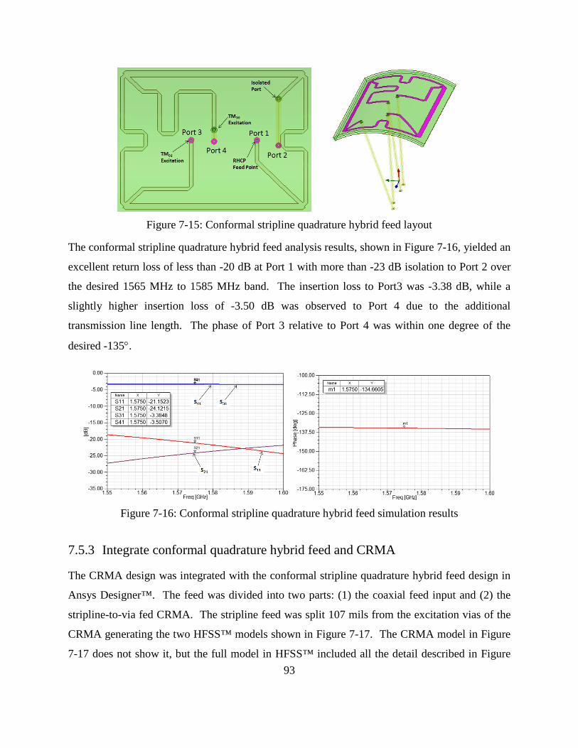
93
Figure 7-15: Conformal stripline quadrature hybrid feed layout
The conformal stripline quadrature hybrid feed analysis results, shown in Figure 7-16, yielded an
excellent return loss of less than -20 dB at Port 1 with more than -23 dB isolation to Port 2 over
the desired 1565 MHz to 1585 MHz band. The insertion loss to Port3 was -3.38 dB, while a
slightly higher insertion loss of -3.50 dB was observed to Port 4 due to the additional
transmission line length. The phase of Port 3 relative to Port 4 was within one degree of the
desired -135°.
Figure 7-16: Conformal stripline quadrature hybrid feed simulation results
7.5.3 Integrate conformal quadrature hybrid feed and CRMA
The CRMA design was integrated with the conformal stripline quadrature hybrid feed design in
Ansys Designer™. The feed was divided into two parts: (1) the coaxial feed input and (2) the
stripline-to-via fed CRMA. The stripline feed was split 107 mils from the excitation vias of the
CRMA generating the two HFSS™ models shown in Figure 7-17. The CRMA model in Figure
7-17 does not show it, but the full model in HFSS™ included all the detail described in Figure

94
7-7 and Figure 7-8. The stripline waveports of each model were close enough to discontinuity
points in the stripline that higher order modes were included at the port. A total of four modes
were included in the stripline waveports. The HFSS™ models were imported into Designer™,
and the four modes of the stripline waveports in each model were connected as shown in Figure
7-18. The coaxial waveports from the HFSS™ model were terminated as Port 1, the RHCP
excitation port, and Port 2, the isolation port, in Designer™.
(a) Conformal stripline quadrature hybrid feed
(b) Stripline-to-via fed CRMA
Figure 7-17: HFSS™ models for integration in Designer™

95
Designer™ performs a computationally efficient S-parameter network analysis using the already
solved for S-parameters from the full-wave 3D simulations in HFSS™. The resulting Port 1
input return loss was less than -9.54 dB (2:1 VSWR) from 1569 MHz to 1586 MHz as shown in
Figure 7-19. In addition to S-parameters, Designer™ has the ability to “push excitations” back
into the HFSS™ model in order to obtain the radiation patterns of the integrated quadrature
hybrid and CRMA model. The radiation pattern of the integrated quadrature hybrid and CRMA
at 1575 MHz is shown in Figure 7-20.
Figure 7-18: Designer™ integration of HFSS™ quadrature hybrid and CRMA

96
Figure 7-19: Quadrature hybrid and CRMA simulated input return loss
Figure 7-20: Quadrature hybrid and CRMA simulated 1575 MHz RHCP pattern

97
The integrated gain (IG) of the integrated quadrature hybrid and CRMA was computed at 1565
MHz, 1575 MHz and 1585 MHz. A plot of the RHCP IG is given in Figure 7-21. The IG
includes 0.5 dB of loss for the feed network based on the results from the conformal stripline
quadrature hybrid feed in Figure 7-16. The requirement for 50% sky coverage with an IG of at
least -6 dBic is met at 1575 MHz with coverage of 51%. At 1565 MH and 1585 MHz, the sky
coverage with an IG of at least -6 dBic drops below the requirement to 43% and 26%
respectively.
Figure 7-21: Quadrature hybrid and CRMA simulated RHCP integrated gain

98
7.6 Design Compliance
A compliance matrix for the resulting CRMA design with integrated quadrature hybrid feed is
given in Table 7-2.
Table 7-2: Compliance matrix for CP CRMA design
Parameter Requirement Compliance
Center Frequency (f0) 1575.42 MHz for L1 YES
Operating Bandwidth +/ - 10.23 MHz YES
Polarization Right Hand Circular
Polarized (RHCP) YES
Integrated Gain (IG) -
minimum
-6 dBic
(50% sky coverage)
NO Meets requirement at 1575 MHz, but not at low and high end of band
Impedance (ohms) 50 ohms nominal YES
Voltage Standing
Wave Ratio (VSWR) 2.0 : 1
NO Meets requirement from 1569 MHz to 1586 MHz
Mechanical Volume Fit within cavity
defined in Figure 7-2 YES
7.7 Summary Remarks
Continued development is required to bring the CRMA design into compliance. The biggest
issue is the narrow impedance bandwidth of the TM10 mode. The best way to achieve wider
performance is typically thicker patch substrates with lower dielectric constants. Unfortunately,
the application requires a very small form factor that will not accommodate a thicker substrate or
lower dielectric constant. Future design iterations should consider coupled or aperture coupled
feeds, parasitic stacked patches, and slots in the patch metal as a means of extending the input
impedance bandwidth of the TM10 mode.

99
CHAPTER 8
CONCLUSION
The modern microstrip antenna was first introduced into the literature in 1972 by Munson [1] to
address the need for “paper thin” antennas that would best suit the aerodynamic and mechanical
engineer for high velocity aircraft, missiles and rockets. Although the microstrip antenna was
first introduced for its ability to conform to the structure of a platform, most of the literature
written since that time focused on the development of planar microstrip antennas as they met the
needs of most applications and were easier to analyze and build. However, the demand for a
singly curved conformal microstrip antenna (SC-CMA) has increased in recent years with the
proliferation of small unmanned aerial system (UAS) and smart missile and munitions platforms.
Existing SC-CMA literature focuses on the development of computational and analytical
approaches for the analysis of the structure. Unfortunately, existing computational and analytical
approaches do not provide the practicing engineer with an easy to implement, accurate and
efficient model to aid in the design and understanding of the SC-CMA. In addition, no existing
literature was found that analyzed the performance of the SC-CMA as the patch metal bend
radius was made electrically small (kb < 1, where k is the free space propagation constant and b
is the bend radius of the patch metal).
In an attempt to fill some of these gaps in the existing literature, this research analyzed the
performance of a rectangular patch SC-CMA as a function of the patch metal bend radius. The
analysis of the rectangular patch SC-CMA or cylindrical rectangular microstrip antenna
(CRMA), as it is commonly called in the literature, led to many significant discoveries and the
development of an accurate and efficient CRMA transmission line model (TLM). The CRMA
TLM provides practicing engineers with an accurate, efficient means of analyzing and
understanding the performance trades associated with the design of a CRMA.
A detailed list of the important contributions made by this research, as well as a list of potential
directions for future work follows.

100
8.1 Contributions
This body of research has made several important contributions to the field of singly curved
conformal microstrip antenna (SC-CMA) theory and design.
1) Developed the first transmission line model (TLM) to accurately and efficiently analyze a
cylindrical rectangular microstrip antenna (CRMA).
A CRMA TLM was developed in Chapter 5 that accurately models the impact of the
patch metal bend radius on the performance of the CRMA. The TM01 and TM10 modes
require separate TLM instantiations, but the impact of the patch metal bend radius on
both modes is easily incorporated into the planar TLM presented by Pues and Van de
Capelle [7]. This is accomplished by scaling the radiating slot normalized length (w) and
width (s) by a function that is inversely proportional to the electrical length of the patch
bend radius. Compared to the cavity model and generalized transmission line model
(GTLM), which are prevalent in the literature, the CRMA TLM is much easier to
implement as it does not require more advanced mathematics such as Green’s functions
or the use of the wave equation and separation of variables. Therefore, the CRMA TLM
provides the practicing antenna engineer with a simple, efficient model from which to
gain significant insight into the operation of the antenna.
2) Quantified the impact of electrically small patch metal bend radii on the performance of
the CRMA.
The Ansys HFSS full-wave 3D electromagnetic analysis of the CRMA in Chapter 4
revealed the considerable impact the patch metal bend radius has on performance. The
impact on performance is greatest at bend radii below half a free space wavelength. This
impact is missing from the existing literature because the CRMA structures studied
typically have patch metal bend radii on the order of a single free space wavelength or
more. This research is the first, to the author’s knowledge, to show the significant
impedance bandwidth increase of the TM01 (axial) mode and the significant resonance
frequency increase of the TM10 (circumferential) mode as the patch metal bend radius is

101
decreased to electrically small levels (kb < 1, where k is the free space propagation
constant and b is the bend radius of the patch metal).
3) Established that the performance impact of the patch metal bend radius was independent
of substrate permittivity and environment changes such as the addition of a cavity.
Three full-wave 3D models were analyzed in Ansys HFSS in Chapter 4. The first
model was a typical CRMA with a substrate and superstrate that subtended the entire
circumference of the cylinder. This model used a high dielectric constant substrate of 16.
The second two models both were placed in cavities to emulate a typical real world
mounting condition. One of the cavity backed (CB) CRMA models used the same high
dielectric constant substrate of 16, while the other used a lower dielectric constant of 3.
All three models were designed to resonate near 1575 MHz, so the lower dielectric
constant had much larger patch metal dimensions. The results from these three models
showed that, when normalized to the performance of an infinitely large radius or planar
instantiation, the performance trends as a function of patch metal bend radius are nearly
identical.
4) Proposed a novel CRMA design approach using the newly developed CRMA TLM in
conjunction with a full-wave 3D model in Ansys HFSS.
A design approach was presented that utilizes the newly developed CRMA TLM to
establish a baseline for detailed analysis within the Ansys HFSS full-wave 3D
simulator. An example design was carried out in Chapter 8 for a right-hand circularly
polarized (RHCP) GPS antenna. The requirements for the antenna come from a
munitions application for precision guidance. Comparing the resulting Ansys HFSS
design to the CRMA TLM starting point, it was noticed that the patch metal dimensions
were off by less than 2%, while the probe feed locations differed by nearly 25%. The
probe feed location differences are attributed to the mutual coupling between ports,
which is not accounted for in the CRMA TLM as it considers each mode separately as if
they have zero coupling.

102
8.2 Future Work
There are many directions one could follow to further advance the state of conformal microstrip
antennas. Specifically, there are a few main areas closely related to the research performed
herein.
1) Quantify the impact of electrically small patch metal bend radii on the performance of
circular or other non-rectangular patch shapes.
This work determined the impact of electrically small patch metal bend radii on the
performance of rectangular patches using Ansys HFSS™, a full-wave 3D
electromagnetic simulator. A similar full-wave 3D electromagnetic analysis could be
performed on a circular or other non-rectangular patch shape to determine its
performance trends as a function of patch metal bend radius.
2) Enhance the newly developed CRMA TLM to account for coupling between the probe
feeds of orthogonal modes in a dual or circular polarization CRMA.
This work developed an accurate TLM for both the TM01 (axial) and TM10
(circumferential) modes of the CRMA. However, this new CRMA TLM does not
account for the coupling between feeds in the case of dual mode excitation. This became
evident in the design of the dual probe fed circularly polarized CRMA in Chapter 7. The
patch dimensions derived from the CRMA TLM were accurate to within 2%, but the
probe feed locations were off by as much as 25%. A single CRMA TLM that includes
both the TM01 and TM10 mode models developed in this research plus a coupling term
would increase the accuracy of the model predicted probe feed location.
3) Perform a characteristic mode analysis of the CRMA structure to gain a better
understanding of the performance changes as a function of patch metal bend radius.
This research revealed trends in the performance of the CRMA as a function of patch
metal bend radius, and we were able to successfully model these trends by simply scaling
the radiating slot dimensions of the planar microstrip antenna TLM. However, a better
understanding of the physics behind the performance trends may lead to an even more
accurate CRMA TLM. Characteristic mode theory (CMT) proposes a set of

103
characteristic current modes that form an orthonormal basis for the current on a metal
structure such as an antenna. A CMT analysis may offer insight into the physics of the
CRMA by revealing differences in the current modes as a function of patch metal bend
radius. A recent review of CMT can be found in [33].
4) Explore methods for increasing the impedance bandwidth of the CRMA, especially the
TM10 mode.
In this research, it was discovered that the CRMA TM01 mode impedance bandwidth
increased as the patch metal bend radius decreased, especially below bend radii of half a
wavelength. However, the CRMA TM10 mode impedance bandwidth remained narrow
and relatively unchanged as the patch metal bend radius decreased. As seen in the
circularly polarized CRMA design example in Chapter 7, the impedance bandwidth of
the TM10 mode must be increased to realize the desired design requirements. Based on
techniques developed for increasing the impedance bandwidth of planar microstrip
antennas, future work may consider aperture coupled feeds, parasitic stacked patches, and
slots in the patch metal as means for extending the input impedance bandwidth of the
CRMA TM10 mode.

104
APPENDIX A
MATLAB CODE
A.1 Probe Fed CRMA
function CRM_TLM(PM1_L,PM1_W,PM1_t,PS1_H,PS1_er,PF1_x,PF1_y,PF1_d,f1,f2,PM_R,mode)
% Calculate input impedance of a Cylindrical Rectangular Microstrip Antenna
% (CRMA) using a 2 slot Transmission Line Model (TLM) derived from the
% planar TLM of Pues and Van de Capelle
%--------------------------------------------------------------------------
% Inputs
% PM1_L = patch metal #1 length (E-Plane) [meters]
% PM1_W = patch metal #1 width (H-Plane) [meters]
% PM1_t = patch metal #1 conductor thickness [meters]
% PS1_H = patch substrate #1 thickness [meters]
% PS1_er = patch substrate #1 relative permittivity
% PF1_x = patch feed #1 x position [meters]
% as referenced to rad edge #1
% positive values move toward rad edge #2
% PF1_y = patch feed #1 y position [meters]
% as referenced to rad edge #3
% positive values move toward rad edge #4
% PF1_d = patch feed #1 diameter [meters]
% f1 = lower operating frequency [Hz]
% f2 = higher operating frequency [Hz]
% PM_R = patch metal bend radius [meters]
% mode = 0 for TM01 or 1 for TM10
%
% Output:
%
%
% Coded by: Brian J. Herting
% University of Illinois

105
%
% Reference: James & Hall "Handbook on Microstrip Antennas, Vol 2"
% Wadell "T-Line Design Handbook"
% Garg, Bhartia, Bahl "Microstrip Design Handbook"
%
% Original: 04 Sept 2012
% Current: 17 March 2014
%--------------------------------------------------------------------------
%% Common constants
eps0 = 8.854e-12; % permittivity of free space
mu0 = 1.25663706144e-6; % permeability of free space
c0 = 1/sqrt(mu0*eps0); % Speed of light in free space
eta = sqrt(mu0/eps0); % impedance of free space in ohms
fop = (f1:1e6:f2)'; % operating frequency range over which to plot the addmittance
w = (2*pi).*fop; % transform frequency to omega in radians/sec
k = w./c0; % propagation constant of free space
%% Determine CRM Line Parameters
% Use analytic equations to determine T-Line parameters
PathName = 'C:\HFSS\PhD\CRMTLM\';
if mode==0 % TM01
snpFileName = ['CRMTLM_TM01_CylR',...
strrep(num2str(PM_R*100,'%.3f'),'.','p'),'_PS1H_',...
strrep(num2str(PS1_H/0.0254,'%.3f'),'.','p'),'.s1p'];
else
snpFileName = ['CRMTLM_TM10_CylR',...
strrep(num2str(PM_R*100,'%.3f'),'.','p'),'_PS1H_',...
strrep(num2str(PS1_H/0.0254,'%.3f'),'.','p'),'.s1p'];
end
[eps_eff,Z0] = uStrip_TLParams(PM1_W,PS1_H,PS1_er,fop);
alpha = 0;
beta = k.*sqrt(eps_eff);
gamma = alpha+1i.*beta;
Y0 = 1./Z0;
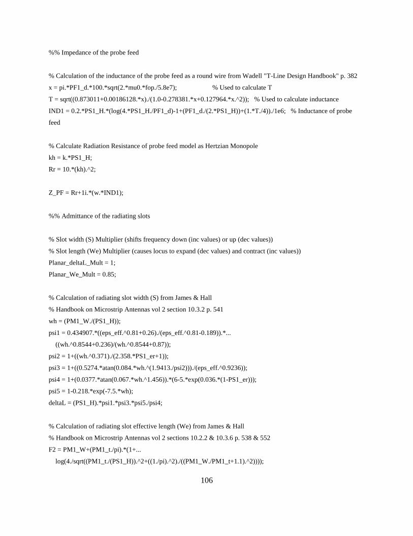
106
%% Impedance of the probe feed
% Calculation of the inductance of the probe feed as a round wire from Wadell "T-Line Design Handbook" p. 382
x = pi.*PF1_d.*100.*sqrt(2.*mu0.*fop./5.8e7); % Used to calculate T
T = sqrt((0.873011+0.00186128.*x)./(1.0-0.278381.*x+0.127964.*x.^2)); % Used to calculate inductance
IND1 = 0.2.*PS1_H.*(log(4.*PS1_H./PF1_d)-1+(PF1_d./(2.*PS1_H))+(1.*T./4))./1e6; % Inductance of probe
feed
% Calculate Radiation Resistance of probe feed model as Hertzian Monopole
kh = k.*PS1_H;
Rr = 10.*(kh).^2;
Z_PF = Rr+1i.*(w.*IND1);
%% Admittance of the radiating slots
% Slot width (S) Multiplier (shifts frequency down (inc values) or up (dec values))
% Slot length (We) Multiplier (causes locus to expand (dec values) and contract (inc values))
Planar_deltaL_Mult = 1;
Planar_We_Mult = 0.85;
% Calculation of radiating slot width (S) from James & Hall
% Handbook on Microstrip Antennas vol 2 section 10.3.2 p. 541
wh = (PM1_W./(PS1_H));
psi1 = 0.434907.*((eps_eff.^0.81+0.26)./(eps_eff.^0.81-0.189)).*...
((wh.^0.8544+0.236)/(wh.^0.8544+0.87));
psi2 = 1+((wh.^0.371)./(2.358.*PS1_er+1));
psi3 = 1+((0.5274.*atan(0.084.*wh.^(1.9413./psi2)))./(eps_eff.^0.9236));
psi4 = 1+(0.0377.*atan(0.067.*wh.^1.456)).*(6-5.*exp(0.036.*(1-PS1_er)));
psi5 = 1-0.218.*exp(-7.5.*wh);
deltaL = (PS1_H).*psi1.*psi3.*psi5./psi4;
% Calculation of radiating slot effective length (We) from James & Hall
% Handbook on Microstrip Antennas vol 2 sections 10.2.2 & 10.3.6 p. 538 & 552
F2 = PM1_W+(PM1_t./pi).*(1+...
log(4./sqrt((PM1_t./(PS1_H)).^2+((1./pi).^2)./((PM1_W./PM1_t+1.1).^2))));

107
F1 = 6+(2.*pi-6).*exp(-((4.*pi.^2)./3).*(((PS1_H)./F2).^(3./4)));
W2 = (2.*pi.*(PS1_H))./(log((PS1_H).*F1./F2+sqrt(1+(2.*(PS1_H)./F2).^2)));
Sw = c0.^2./(4.*fop.^2.*(eps_eff-1));
Pw = (PM1_L./3).^3+(Sw./2).*(W2-PM1_L./3);
Qw = (Sw./3)-(PM1_L./3).^2;
Rw = (Pw.^2+Qw.^3).^(1./2);
We = ((PM1_L./3)+(Rw+Pw).^(1./3)-(Rw-Pw).^(1./3));
switch mode
case 0 % TM01
deltaL = deltaL.*(0.0098./(PM_R./(c0./fop))+1).*Planar_deltaL_Mult;
We = We.*(0.0936./(PM_R./(c0./fop))+1).*Planar_We_Mult;
case 1 % TM10
deltaL = deltaL.*(-0.0482./(PM_R./(c0./fop))+1).*Planar_deltaL_Mult;
We = We.*(-0.0114./(PM_R./(c0./fop))+1).*Planar_We_Mult;
end
% Calculation of rad edge #1 slot radiator self admittance
% James/Hall Hdbk on Mstrip Ants vol 2 section 10.3-10.3.3 (p. 538-544)
w1 = k.*We; % Normalized length of the slot resonator
s = k.*deltaL; % Normalized width of the slot resonator
Si = sinint(w1); % Sine integral required to calculate G_S
B_S1 = real(Y0).*tan(beta.*deltaL); % Susceptance of radiating slot
G_S1 = (1./pi./eta).*... % Conductance of radiating slot
((w1.*Si+sin(w1)./w1+cos(w1)-2).*(1-s.^2./24)+(s.^2./12).*...
(1./3+cos(w1)./w1.^2-sin(w1)./w1.^3));
% Calculation of rad edge #2 slot radiator self admittance
% Same as rad edge #1
B_S2 = B_S1;
G_S2 = G_S1;
% Calculation of rad slot mutual admittance
% James/Hall Hdbk on Mstrip Ants vol 2 section 10.3.4-10.3.5 (p. 544-551)
Le = PM1_L+deltaL; % Center distance between two radiating slots
l = k.*Le; % Normalized center distance

108
Fg = besselj(0,l)+... % Auxilary coupling function for mutual conductance G_M
s.^2./(24-s.^2).*besselj(2,l);
Kg = 1; % Correction factor for Fg
Fb = pi./2.*... % Auxilary coupling function for mutual susceptance B_M
(bessely(0,l)+s.^2./(24-s.^2).*bessely(2,l))./...
(log(s./2)+0.577216-3/2+s.^2./12./(24-s.^2)); % 0.577216 = Euler's constant (Ce)
Kb = 1-exp(-0.21.*w1); % Correction factor for Fb
G_M1 = G_S1.*Fg.*Kg;
B_M1 = B_S1.*Fb.*Kb;
G_M2 = G_S2.*Fg.*Kg;
B_M2 = B_S2.*Fb.*Kb;
% Admittance of radiating slot #1
Y_S1 = G_S1+G_M1+1i.*(B_S1+B_M1);
% Admittance of radiating slot #2
Y_S2 = G_S2+G_M2+1i.*(B_S2+B_M2);
%% Transform slot admittances to feed point
% Admittance at feed point due to radiating slot #1
YL = Y_S1;
L = PF1_x;
Yin1 = Y0.*(YL+Y0.*tanh(gamma.*L))./(Y0+YL.*tanh(gamma.*L));
% Admittance at feed point due to radiating slot #2
YL = Y_S2;
L = PM1_L-PF1_x;
Yin2 = Y0.*(YL+Y0.*tanh(gamma.*L))./(Y0+YL.*tanh(gamma.*L));
%% Calculate CRM input impedance and S11
% Calculate input impedance
Zin = Z_PF+1./(Yin1+Yin2);
Z_RE = real(Zin);
Z_IM = imag(Zin);
S11 = (Zin-50)./(Zin+50);

109
S11dB = 20.*log10(abs(S11));
%% Save touchstone S-parameter data to snpFileName
temp = dir([PathName,snpFileName]);
n = 0;
while ~isempty(temp)
n=n+1;
if n==1
snpFileName = [snpFileName(1:end-4),'_',sprintf('%02d',n),'.s1p'];
else
snpFileName = [snpFileName(1:end-7),'_',sprintf('%02d',n),'.s1p'];
end
temp = dir([PathName,snpFileName]);
end
clear temp
% Save result to *.s1p touchstone file
s1pHeader = '# GHz S RI R 50';...
'! S-Parameters data';...
'! Freq reS11 imS11';
fid = fopen([PathName,snpFileName], 'w');
for ind = 1:size(s1pHeader,1)
fprintf(fid,'%s\n',s1pHeaderind,:);
end
for ind = 1:size(fop,1)
fprintf(fid,'%.10f %.10f %.10f\n',...
fop(ind)/1e9,real(S11(ind)),imag(S11(ind)));
end
fclose(fid);
%% Plot results
% Plot input impedance vs frequency
figure
plot(fop./1e9,Z_IM,'-b','LineWidth',2,'DisplayName','Im[Z]')
hold on
plot(fop./1e9,Z_RE,'--r','LineWidth',2,'DisplayName','Re[Z]')

110
hold off
xlabel('Freq (GHz)')
ylabel('Z_in (\Omega)')
str1 = [num2str(PM1_L),' ',num2str(PM1_W),' ',num2str(PM1_t),' ',...
num2str(PS1_H),' ',num2str(PS1_er)];
title('Z_in vs. Freq';str1)
legend
grid on
% Plot return loss (S11) vs frequency
figure
plot(fop./1e9,S11dB,'-b','LineWidth',2,'DisplayName','S11')
xlabel('Freq (GHz)')
ylabel('Return Loss (dB)')
str1 = [num2str(PM1_L),' ',num2str(PM1_W),' ',num2str(PM1_t),' ',...
num2str(PS1_H),' ',num2str(PS1_er)];
title('Return Loss vs. Freq';str1)
legend
grid on
A.2 Microstrip Line Fed CRMA
function
CRM_TLM_uStripEdgeFed(PM1_L,PM1_W,PM1_t,PS1_H,PS1_er,TLine1_W,TLine1_L,TLine2_W,TLine2_L,f1,
f2,PM_R,mode)
% Calculate input impedance of a Cylindrical Rectangular Microstrip Antenna
% (CRMA) using a 2 slot Transmission Line Model (TLM) derived from the
% planar TLM by Pues and Van de Capelle
%--------------------------------------------------------------------------
% Inputs
% PM1_L = patch metal #1 length (E-plane) [meters]
% PM1_W = patch metal #1 width (H-plane) [meters]
% PM1_t = patch metal #1 conductor thickness [meters]
% PS1_H = patch substrate #1 thickness [meters]
% PS1_er = patch substrate #1 relative permittivity

111
% TLine1_W = uStrip TLine #1 width [meters]
%
% TLine1_L = uStrip TLine #1 length [meters]
% as referenced to rad edge #2
% TLine2_W = uStrip TLine #2 width [meters]
%
% TLine2_L = uStrip TLine #2 length [meters]
% as referenced to TLine #1
% f1 = lower operating frequency [Hz]
% f2 = higher operating frequency [Hz]
% PM_R = patch metal bend radius [meters]
% mode = 0 for TM01 or 1 for TM10
%
% Output:
%
%
% Coded by: Brian J. Herting
% University of Illinois
%
% Reference: James & Hall "Handbook on Microstrip Antennas, Vol 2"
% Wadell "T-Line Design Handbook"
% Garg, Bhartia, Bahl "Microstrip Design Handbook"
%
% Original: 10 Nov 2013
% Current: 17 March 2014
%--------------------------------------------------------------------------
%% Common constants
eps0 = 8.854e-12; % permittivity of free space
mu0 = 1.25663706144e-6; % permeability of free space
c0 = 1/sqrt(mu0*eps0); % Speed of light in free space
eta = sqrt(mu0/eps0); % impedance of free space in ohms
fop = (f1:1e6:f2)'; % operating frequency range over which to plot the admittance
w = (2*pi).*fop; % transform frequency to omega in radians/sec
k = w./c0; % propagation constant of free space

112
%% Determine the CRM Line Parameters
% Use analytic equations to determine T-Line parameters
PathName = 'C:\HFSS\PhD\Ruyle\';
if mode==0 % TM01
snpFileName = ['CRMTLM_uStripFeed_TM01_CylR_',...
strrep(num2str(PM_R*100,'%.3f'),'.','p'),'_PSH_'...
strrep(num2str(PS1_H/0.0254,'%.3f'),'.','p'),'.s1p'];
else
snpFileName = ['CRMTLM_uStripFeed_TM10_CylR',...
strrep(num2str(PM_R*100,'%.3f'),'.','p'),'_PSH_'...
strrep(num2str(PS1_H/0.0254,'%.3f'),'.','p'),'.s1p'];
end
[eps_eff,Z0] = uStrip_TLParams(PM1_W,PS1_H,PS1_er,fop);
alpha = 0;
beta = k.*sqrt(eps_eff);
gamma = alpha+1i.*beta;
Y0 = 1./Z0;
%% Admittance of the radiating slots
% Slot width (S) Multiplier (shifts frequency down (inc values) or up (dec values))
% Slot length (We) Multiplier (causes locus to expand (dec values) and contract (inc values))
Planar_deltaL_Mult = 1.29;
Planar_We_Mult = 1.07;
% Calculation of radiating slot width (S) from James & Hall
% Handbook on Microstrip Antennas vol 2 section 10.3.2 p. 541
wh = (PM1_W./(PS1_H));
psi1 = 0.434907.*((eps_eff.^0.81+0.26)./(eps_eff.^0.81-0.189)).*...
((wh.^0.8544+0.236)/(wh.^0.8544+0.87));
psi2 = 1+((wh.^0.371)./(2.358.*PS1_er+1));
psi3 = 1+((0.5274.*atan(0.084.*wh.^(1.9413./psi2)))./(eps_eff.^0.9236));
psi4 = 1+(0.0377.*atan(0.067.*wh.^1.456)).*(6-5.*exp(0.036.*(1-PS1_er)));
psi5 = 1-0.218.*exp(-7.5.*wh);
deltaL = (PS1_H).*psi1.*psi3.*psi5./psi4;
113
% Calculation of radiating slot effective length (We) from James & Hall
% Handbook on Microstrip Antennas vol 2 sections 10.2.2 & 10.3.6 p. 538 & 552
Wp = PM1_W+(PM1_t./pi).*(1+...
log(4./sqrt((PM1_t./(PS1_H)).^2+((1./pi).^2)./((PM1_W./PM1_t+1.1).^2))));
F = 6+(2.*pi-6).*exp(-((4.*pi.^2)./3).*(((PS1_H)./Wp).^(3./4)));
We0 = (2.*pi.*(PS1_H))./(log((PS1_H).*F./Wp+sqrt(1+(2.*(PS1_H)./Wp).^2)));
Sw = c0.^2./(4.*fop.^2.*(eps_eff-1));
Pw = (PM1_L./3).^3+(Sw./2).*(We0-PM1_L./3);
Qw = (Sw./3)-(PM1_L./3).^2;
Rw = (Pw.^2+Qw.^3).^(1./2);
We = ((PM1_L./3)+(Rw+Pw).^(1./3)-(Rw-Pw).^(1./3));
switch mode
case 0 % TM01
deltaL = deltaL.*(0.0098./(PM_R./(c0./fop))+1).*Planar_deltaL_Mult;
We = We.*(0.0936./(PM_R./(c0./fop))+1).*Planar_We_Mult;
case 1 % TM10
deltaL = deltaL.*(-0.0482./(PM_R./(c0./fop))+1).*Planar_deltaL_Mult;
We = We.*(-0.0114./(PM_R./(c0./fop))+1).*Planar_We_Mult;
end
% Calculation of rad edge #1 slot radiator self admittance
% James/Hall Hdbk on Mstrip Ants vol 2 section 10.3-10.3.3 (p. 538-544)
w1 = k.*We; % Normalized length of the slot resonator
s = k.*deltaL; % Normalized width of the slot resonator
Si = sinint(w1); % Sine integral required to calculate G_S
B_S1 = real(Y0).*tan(beta.*deltaL); % Susceptance of radiating slot
G_S1 = (1./pi./eta).*... % Conductance of radiating slot
((w1.*Si+sin(w1)./w1+cos(w1)-2).*(1-s.^2./24)+(s.^2./12).*...
(1./3+cos(w1)./w1.^2-sin(w1)./w1.^3));
% Calculation of rad edge #2 slot radiator self admittance
% Same as rad edge #1
B_S2 = B_S1;
G_S2 = G_S1;

114
% Calculation of rad slot mutual admittance
% James/Hall Hdbk on Mstrip Ants vol 2 section 10.3.4-10.3.5 (p. 544-551)
Le = PM1_L+deltaL; % Center distance between two radiating slots
l = k.*Le; % Normalized center distance
Fg = besselj(0,l)+... % Auxilary coupling function for mutual conductance G_M
s.^2./(24-s.^2).*besselj(2,l);
Kg = 1; % Correction factor for Fg
Fb = pi./2.*... % Auxilary coupling function for mutual susceptance B_M
(bessely(0,l)+s.^2./(24-s.^2).*bessely(2,l))./...
(log(s./2)+0.577216-3/2+s.^2./12./(24-s.^2)); % 0.577216 = Euler's constant (Ce)
Kb = 1-exp(-0.21.*w1); % Correction factor for Fb
G_M1 = G_S1.*Fg.*Kg;
B_M1 = B_S1.*Fb.*Kb;
G_M2 = G_S2.*Fg.*Kg;
B_M2 = B_S2.*Fb.*Kb;
% Admittance of radiating slot #1
Y_S1 = G_S1+G_M1+1i.*(B_S1+B_M1);
% Admittance of radiating slot #2
Y_S2 = G_S2+G_M2+1i.*(B_S2+B_M2);
%% Transform slot admittances to feed point
% Admittance at feed point due to radiating slot #1
YL = Y_S1;
L = PM1_L;
Yin1 = Y0.*(YL+Y0.*tanh(gamma.*L))./(Y0+YL.*tanh(gamma.*L));
% Admittance at feed point due to radiating slot #2
YL = Y_S2;
L = 0;
Yin2 = Y0.*(YL+Y0.*tanh(gamma.*L))./(Y0+YL.*tanh(gamma.*L));
%% Calculate CRM input impedance and S11

115
% Admittance at TLine #1 / TLine #2 interface
% Use analytic equations to determine T-Line parameters
[eps_eff1,Z01] = uStrip_TLParams(TLine1_W,PS1_H,PS1_er,fop);
alpha1 = 0;
beta1 = k.*sqrt(eps_eff1);
gamma1 = alpha1+1i.*beta1;
Y01 = 1./Z01;
YL = Yin1+Yin2;
L = TLine1_L;
Yin = Y01.*(YL+Y01.*tanh(gamma1.*L))./(Y01+YL.*tanh(gamma1.*L));
% Admittance at TLine #2 excitation point
% Use analytic equations to determine T-Line parameters
[eps_eff2,Z02] = uStrip_TLParams(TLine2_W,PS1_H,PS1_er,fop);
alpha2 = 0;
beta2 = k.*sqrt(eps_eff2);
gamma2 = alpha2+1i.*beta2;
Y02 = 1./Z02;
YL = Yin;
L = TLine2_L;
Yin = Y02.*(YL+Y02.*tanh(gamma2.*L))./(Y02+YL.*tanh(gamma2.*L));
% Calculate input impedance
Zin = 1./Yin;
Z_RE = real(Zin);
Z_IM = imag(Zin);
S11 = (Zin-50)./(Zin+50);
S11dB = 20.*log10(abs(S11));
%% Save touchstone S-parameter data to snpFileName
temp = dir([PathName,snpFileName]);
n = 0;
while ~isempty(temp)
n=n+1;
if n==1
snpFileName = [snpFileName(1:end-4),'_',sprintf('%02d',n),'.s1p'];

116
else
snpFileName = [snpFileName(1:end-7),'_',sprintf('%02d',n),'.s1p'];
end
temp = dir([PathName,snpFileName]);
end
clear temp
% Save result to *.s1p touchstone file
s1pHeader = '# GHz S RI R 50';...
'! S-Parameters data';...
'! Freq reS11 imS11';
fid = fopen([PathName,snpFileName], 'w');
for ind = 1:size(s1pHeader,1)
fprintf(fid,'%s\n',s1pHeaderind,:);
end
for ind = 1:size(fop,1)
fprintf(fid,'%.10f %.10f %.10f\n',...
fop(ind)/1e9,real(S11(ind)),imag(S11(ind)));
end
fclose(fid);
%% Plot results
% Plot input impedance vs frequency
figure
plot(fop./1e9,Z_IM,'-b','LineWidth',2,'DisplayName','Im[Z]')
hold on
plot(fop./1e9,Z_RE,'--r','LineWidth',2,'DisplayName','Re[Z]')
hold off
xlabel('Freq (GHz)')
ylabel('Z_in (\Omega)')
str1 = [num2str(PM1_L),' ',num2str(PM1_W),' ',num2str(PM1_t),' ',...
num2str(PS1_H),' ',num2str(PS1_er),' ',num2str(TLine1_W),' ',...
num2str(TLine1_L),' ',num2str(TLine2_W),' ',num2str(TLine2_L)];
title('Z_in vs. Freq';str1)
legend

117
grid on
% Plot return loss vs frequency
figure
h = plot(fop./1e9,S11dB);
set(h,'Color','b','LineWidth',2,'DisplayName','S_11')
% set(gca,'XTick',tickmarks)
xlabel('Freq (GHz)')
ylabel('Return Loss (dB)')
title('Return Loss vs. Freq for ';str1)
grid on
A.3 Transmission Line Parameters
function [eps_eff,Z0] = uStrip_TLParams(w,h,er,fop)
% Calculate effective permittivity and characteristic impedance of a planar
% microstrip transmission line with width (w), substrate height (h), and
% substrate relative permittivity (er) over frequency (fop).
% Equations taken from Rogers Corp white paper
% http://www.rogerscorp.cn/documents/780/acm/Design-Data-for-Microstrip-Transmission-Lines-on-RT-duroid-
Laminates.aspx
% First proposed by Wheeler and Schneider and later improved by
% Hammerstad and Jensen and once again by
% Kirschning and Jansen.
%--------------------------------------------------------------------------
% Inputs
% w = microstrip transmission line width [meters]
% h = substrate height [meters]
% er = substrate relative permittivity [Hz]
% fop = operating frequency
%
% Output:
% eps_eff = effective relative permittivity
% Z0 = characteristic impedance [ohms]
%

118
% Coded by: Brian J. Herting
% University of Illinois
%
% Reference: http://www.rogerscorp.cn/documents/780/acm/Design-Data-for-
% Microstrip-Transmission-Lines-on-RT-duroid-Laminates.aspx
%
% Original: 04 Nov 2013
% Current: 04 Nov 2013
%--------------------------------------------------------------------------
%% Common constants
eps0 = 8.854e-12; % permittivity of free space
mu0 = 1.25663706144e-6; % permeability of free space
c0 = 1/sqrt(mu0*eps0); % Speed of light in free space
eta = sqrt(mu0/eps0); % impedance of free space in ohms
%% Begin code to find TLine Params
U = w./h;
Au = 1+log((U.^4+U.^2./2704)./(U.^4+0.432))./49+log((U./18.1).^3+1)./18.7;
Ber = 0.564.*((er-0.9)./(er+3)).^0.053;
Y = (er+1)./2+((er-1)./2).*(1+10./U).^(-Au.*Ber);
Z01 = eta.*log((6+(2.*pi-6).*exp(-(30.667./U).^0.7528))./U+...
(4./U.^2+1).^0.5)./(2.*pi);
Z0dc = Z01./Y.^0.5;
eps_effdc = Y;
P1 = 0.27488+U.*(0.6315+0.525.*(15.7e-9.*fop.*h+1).^(-20))-...
0.065683.*exp(-8.7513.*U);
P2 = 0.33622.*(1-exp(-0.03442.*er));
P3 = 0.0363.*exp(-4.6.*U).*(1-exp(-(fop.*h.*1e-6./38.7).^4.97));
P4 = 2.751.*(1-exp(-(er./15.916).^8))+1;
P = P1.*P2.*((fop.*h.*1e-6).*(0.1844+P3.*P4)).^1.5763;
eps_eff = er-(er-eps_effdc)./(1+P);
Z0 = Z0dc.*(eps_effdc./eps_eff).^0.5.*((eps_eff-1)./(eps_effdc-1));

119
REFERENCES
[1] R. E. Munson, “Conformal microstrip antennas and microstrip phased arrays”, IEEE Transactions on Antennas and Propagation, On page(s): 74 – 78, Volume: 22 Issue: 1, January 1974.
[2] Y. T. Lo, D. Solomon, and W. F. Richards, “Theory and experiment on microstrip antennas”, IEEE Transactions on Antennas and Propagation, On page(s): 137 – 145, Volume: 27 Issue: 2, March 1979.
[3] R. Garg, P. Bhartia, and I. Bahl, Microstrip Antenna Design Handbook. Boston: Artech House, 2001.
[4] J. R. James and P. S. Hall, Handbook of Microstrip Antennas. London: Peter Peregrinus Ltd., 1989.
[5] D. M. Pozar and D. H. Schaubert, Microstrip Antennas: The Analysis and Design of Microstrip Antennas and Arrays. New Jersey: IEEE Press, 1995.
[6] A. Derneryd, “A theoretical investigation of the rectangular microstrip antenna element”, IEEE Transactions on Antennas and Propagation, On page(s): 532 – 535, Volume: 26 Issue: 4, July 1978.
[7] H. Pues and A. Van de Capelle, “Accurate transmission-line model for the rectangular microstrip antenna”, IEE Proceedings H Microwaves, Optics, and Antennas, On page(s): 334 – 340, Volume: 131 Issue: 6, December 1984.
[8] B. M. Alarjani and J. S. Dahele, “Feed reactance of rectangular microstrip antenna with probe feed”, Electronic Letters, On page(s): 388 – 390, Volume: 36 Issue: 5, March 2000.
[9] D. M. Pozar, “Microstrip antenna aperture-coupled to a microstripline”, Electronics Letters, On page(s): 49 – 50, Volume: 21 Issue: 2, January 1985.
[10] A. Sabban, “A new broadband stacked two-layer microstrip antenna”, in proceedings of Antennas and Propagation Society International Symposium, On page(s): 63 – 66, Volume: 21, May 1983.
[11] C. H. Chen, A. Tulintseff, and R. M. Sorbello, “Broadband two-layer microstrip antenna”, in proceeding of Antennas and Propagation Society International Symposium, On page(s): 251 – 254, Volume: 22, June 1984.
[12] A. S. Elkorany, A. A. Sharshar, and S. M. Elhalafawy, “Ultra wideband stacked microstrip patch antenna”, in proceeding of 3rd European Conference on Antennas and Propagation, On page(s): 1464 – 1466, March 2009.

120
[13] T. Huynh and K. -F. Lee, “Single-layer single-patch wideband microstrip antenna”, Electronics Letters, On page(s): 1310 – 1312, Volume: 31 Issue: 16, August 1995.
[14] S. Weigand, G. H. Huff, K. H. Pan, and J. T. Bernhard, “Analysis and design of broad-band single-layer rectangular U-slot microstrip patch antennas”, IEEE Transactions on Antennas and Propagation, On page(s): 457 – 468, Volume: 51 Issue: 3, March 2003.
[15] S. D. Targonski and D. M. Pozar, “Design of wideband circularly polarized aperture-coupled microstrip antennas”, IEEE Transactions on Antennas and Propagation, On page(s): 214 – 220, Volume: 41 Issue: 2, February 1993.
[16] K. Tong and T. Wong, “Circularly polarized U-Slot antenna”, IEEE Transactions on Antennas and Propagation, On page(s): 2382 – 2385, Volume: 55 Issue: 8, August 2007.
[17] S. L. S. Yang, K. F. Lee, A. A. Kishk, and K. M. Luk, “Design and study of wideband single feed circularly polarized microstrip antennas”, Progress in Electromagnetics Research, On page(s): 45 – 61, Volume: 80, 2008.
[18] K. Y. Lam, K. Luk, K. F. Lee, H. Wong, and K. B. Ng, “Small circularly polarized U-slot wideband patch antenna”, IEEE Antennas and Wireless Propagation Letters, On page(s): 87 – 90, Volume: 10, February 2011.
[19] K. L. Wong, Design of Nonplanar Microstrip Antennas and Transmission Lines. New York: John Wiley & Sons, Inc., 1999.
[20] C. Krowne, “Cylindrical-rectangular microstrip antenna radiation efficiency based on cavity Q factor”, in proceedings of Antennas and Propagation Society International Symposium, On page(s): 11 – 14, Volume: 19, June 1981.
[21] C. Krowne, “Cylindrical-rectangular microstrip antenna”, IEEE Transactions on Antennas and Propagation, On page(s): 194 – 199, Volume: 31 Issue: 1, January 1983.
[22] K. Y. Wu and J. Kauffman, “Radiation pattern computations for cylindrical-rectangular microstrip antennas”, in proceedings of Antennas and Propagation Society International Symposium, On page(s): 39 – 42, Volume: 21, May 1983.
[23] K. M. Luk, K. F. Lee, and J. S. Dahele, “Analysis of the cylindrical-rectangular patch antenna”, IEEE Transactions on Antennas and Propagation, On page(s): 143 – 147, Volume: 37 Issue: 2, February 1989.
[24] A. C. C. Lima and A. J. Giarola, “Cylindrical-rectangular microstrip antenna with the patch along a helical direction”, in proceedings of Antennas and Propagation Society International Symposium, On page(s): 346 – 349, Volume: 1, June 1991.
[25] J. S. Chen and K. L. Wong, “Theory and experiment of slot-coupled cylindrical rectangular and circular microstrip antennas”, in proceedings of Antennas and Propagation Society International Symposium, On page(s): 688 – 691, Volume: 1, July 1996.

121
[26] M. V. T. Heckler, M. Bonadiman, R. Schildberg, L. Cividanes, and J. C. S. Lacava, “CAD package to design rectangular probe-fed microstrip antennas conformed on cylindrical structures”, in proceedings of Microwave and Optoelectronics International Conference, On page(s): 747 – 752, Volume: 2, September 2003.
[27] A. F. T. Salazar, M. Heckler, D. Nascimento, R. Schildberg, and J. C. da S. Lacava, “CYLINDRICAL: an effective CAD package for designing probe-fed rectangular microstrip antennas conformed onto cylindrical structures”, Antennas and Propagation Magazine, On page(s): 164 – 169, Volume: 50 Issue: 1, February 2008.
[28] A. K. Bhattacharyya and R. Garg, “Generalised transmission line model for microstrip patches”, IEE Proceedings H Microwaves, Antennas, and Propagation, On page(s): 93 – 98, Volume: 132 Issue: 2, April 1985.
[29] A. V. Lietuvninkas, V. K. Howe, H. H. Sigmarsson and J. E. Ruyle, “Investigation of conformal antenna design limits”, in proceedings of Antenna Applications Symposium, On page(s): 57 – 74, September 2013.
[30] B. C. Wadell, Transmission Line Design Handbook. Boston: Artech House, 1991.
[31] Rogers Corporation, Width and Effective Dielectric Constant Equations for Design of Microstrip Transmission Lines [Online]. Available: http://www.rogerscorp.com/acm/literature.aspx
[32] P. J. Burke and A. Pergolizzi, XM1156 Precision Guidance Kit (PGK) Overview [Online]. Available: http://www.dtic.mil/ndia/2010fuze/IVAPergolizzi.pdf
[33] M. Cabedo-Fabres, E. Antonino-Daviu, A. Valero-Nogueira and M. F. Bataller, “The theory of characteristic modes revisited: A contribution to the design of antennas for modern applications,” Antennas and Propagation Magazine, On page(s): 52-68, Volume: 49 Issue: 5, October 2007.