an44142a driver ic for 3-phase brushless motor€¦ · page 1 of 48 an44142a product standards tri...
TRANSCRIPT
Page 1 of 48
AN44142A
Product Standards
TRI
H1H
H1L
FR
VSPL
VSP
BC2
U
V
RCS
W
VCC
SS
T
FG
SE
L
PS
RD
S
OV
S
BC
1
RD
FG
SLE
EP
VR
EG
GN
D
VP
UM
P
CVREG
RRCS
CBC
RVH1
CVCC
CVCC1
Condition: VCC = 12 V, VFR = 0 V, VVSP = PWM mode (60kHz,Duty60%)
AN44142A 3-phase full-wave sine-wave PWM drive
VU
VV
VW
IU IV IW
time [s] 2ms/div
CVPUMP
RFGRRD
1 2 3 4 5 6
12
11
10
9
8
7
18 17 16 15 14 13
19
20
21
22
23
24
CFGSEL
CSST
CTRI
( )CVSP
CH ( )
Driver IC for 3-phase Brushless Motor
FEATURES Supply voltage range: 4.5 V ~ 26.4 V Built-in 5-V regulator 3-phase full-wave sine-wave PWM drive by 1-Hall-sensor Selectable Input Mode: Either linear voltage input or PWM input through VSP pin Controllable lower limit for linear voltage input mode through VSPL pin Conduction angle auto driver phase shift correction Rotation direction selectable (Forward/Reverse) FG pulse divide selectable Sleep mode Various protection functions:
Under Voltage Lock Out (UVLO), Over Voltage Lock Out (OVLO), Thermal protection, Over Load Protection, and Over Current Protection
DESCRIPTION AN44142A is a driver IC for 3-phase brushless motor optimized for fan motors.
By employing the rotor position detector and sine wave PWM drive by 1-Hall-sensor, this IC achieves component reduction and miniaturization of motor set as well as motor drive at low noise, low vibration and low power consumption.
Driver IC for 3-phase brushless fan motor
APPLICATIONS
TYPICAL APPLICATION
Notes: The application circuit is an example. The operation of the mass production set is not guaranteed. Sufficient evaluation and verification is required in the design of the mass production set. The Customer is fullyresponsible for the incorporation of the above illustrated application circuit in the design of the equipment.
Doc No. TA4-EA-06255Revision. 2
Established : 2014-05-14Revised : 2014-07-08

Page 2 of 48
AN44142A
Product Standards
FEATURES ................................................................................................................ 1
DESCRIPTION ........................................................................................................... 1
APPLICATIONS ......................................................................................................... 1
TYPICAL APPLICATION ........................................................................................... 1
TYPICAL CHARACTERISTICS ................................................................................. 1
CONTENTS ................................................................................................................ 2
ABSOLUTE MAXIMUM RATINGS ............................................................................ 3
POWER DISSIPATION RATING ............................................................................... 3
RECOMMENDED OPERATING CONDITIONS ........................................................ 4
ELECTRICAL CHARACTERISTICS ......................................................................... 5
PIN FUNCTIONS ........................................................................................................ 9
PIN CONFIGURATION .............................................................................................. 9
FUNCTIONAL BLOCK DIAGRAM ............................................................................ 10
OPERATION .............................................................................................................. 11
AREA OF SAFE OPERATION .................................................................................. 33
PIN EQUIVALENT CIRCUIT ....................................................................................... 34
PACKAGE INFORMATION ........................................................................................ 41
IMPORTANT NOTICE ................................................................................................ 44
USAGE PRECAUTIONS ............................................................................................ 46
CONTENTS
Doc No. TA4-EA-06255Revision. 2
Established : 2014-05-14Revised : 2014-07-08

Page 3 of 48
AN44142A
Product Standards
Parameter Symbol Rating Unit Notes
Supply voltage VCC 28 V *1
Operating ambient temperature Topr – 40 ~ + 95 C *2
Storage temperature Tstg – 55 ~ +150 C *2
Input Voltage Range
VVREG – 0.3 ~ 6.0 V *3
VSLEEP,VH1H,VH1L,VFGSEL,
VVSP,VVSPL,VFR,VRDS,VPS,VOVS
– 0.3 ~ 6.0 V —
VTRI ,VSST – 0.3 ~ 6.0 V —
Output Voltage Range
VFG,VRD – 0.3 ~ 6.0 V —
VVREG – 0.3 ~ 6.0 V —
VRCS – 0.3 ~ 6.0 V *4
VBC1 28 V *4
VBC2,Vpump 37 V *4
Output Current Range
IUdc, IVdc, IWdc 600 mA *5
IUpeak, IVpeak, IWpeak 2200 mA *5, *6
IFG,IRD 5 mA —
IVREG -10 mA —
ESD HBM 2 kV —
ABSOLUTE MAXIMUM RATINGS
Notes: This product may sustain permanent damage if subjected to conditions higher than the above stated absolute maximum rating. This rating is the maximum rating and device operating at this range is not guaranteed as it is higher than our stated recommended operating range. When subjected under the absolute maximum rating for a long time, the reliability of the product may be affected.*1:The values under the condition not exceeding the above absolute maximum ratings and the power dissipation.*2: Except for the power dissipation, operating ambient temperature, and storage temperature, all ratings are for Ta = 25.*3: Applying external voltage to this pin is possible only when this pin and VCC pin is connected.
When applying external voltage to this pin, do not exceed the stated ratings even in transient state.*4: Applying external voltage into these pins is prohibited. Do not exceed the stated ratings even in transient state.*5: Applying external voltage into these pins is prohibited. Do not exceed the stated ratings even in transient state.*6: For VCC≧5.6 V, output current of ±2200 mA is only allowed within 100μs.
For VCC<5.6 V, output current of ±1500 mA is only allowed within 100μs.
POWER DISSIPATION RATING
Package j-a j-cPD
(Ta=25 C)PD
(Ta=70 C)
24 pin Plastic Quad Flat Non-leaded Package (QFN type) 56.1 C/W 4.4 C/W 2.22 W 1.42 W
*1: Glass-Epoxy Substrate (2 Layers) : 50 x 50 x 0.8t (mm), Heat dissipation fin: Die-pad, Soldered. (Heat dissipation via 2
layer board)
Notes: For the actual usage, please refer to the PD-Ta characteristics diagram in the package specification, follow the power supplyvoltage, load and ambient temperature conditions to ensure that there is enough margin and the thermal design does not exceed the allowable value.
CAUTIONAlthough this IC has built-in ESD protection circuit, it may still sustain permanent damage if not handled properly. Therefore, proper ESD precautions are recommended to avoid electrostatic damage to the MOS gates.
Doc No. TA4-EA-06255Revision. 2
Established : 2014-05-14Revised : 2014-07-08

Page 4 of 48
AN44142A
Product Standards
Parameter Symbol Min. Typ. Max. Unit Notes
Supply voltage range VCC 4.5 — 26.4 V —
Input voltage range
VSLEEP 0 — VVREG V *1
VH1H 0 — VVREG V *1
VH1L 0 — VVREG V *1
VPS 0 — VVREG V *1
VRDS 0 — VVREG V *1
VOVS 0 — VVREG V *1
VFGSEL 0 — VVREG V *1
VVSP 0 — VVREG V *1
VVSPL 0 — VVREG V *1
VFR 0 — VVREG V *1
External constants
CVCC 4.7 — — F *2,*3
CVCC1 — 0.1 — F *2,*3
CVREG — 0.1 — F *2,*4
CSST 22p 1800p — F *2,*5
CBC — 0.1 — F *2,*4
CVPUMP — 0.1 — F *2,*4
CTRI 220p 390p 1300p F *2,*5
RRCS 0.15 0.22 — *2,*5,*6
RVH — 1k — *2,*5
CFGSEL — 0.01 — F *2,*7
CVSP — 0.1 — F *2,*8
RECOMMENDED OPERATING CONDITIONS
Note: *1: For setting range of input control voltage, refer to Electrical Characteristics (page 5 - 8) and Operation (page 11 - 32).*2: Operation of mass production set is not guaranteed. Perform enough evaluation and verification on the design of mass
production set.*3: Please perform sufficient evaluation and verification to ensure that VCC pin voltage ripple is reduced.*4: It is recommended to use the values indicated.*5: Please choose the setting according to the usage. Please refer to the Electrical Characteristics (page 5 - 8) and Operation
(page 11 - 32).*6: Do not use resistor of value smaller than this. When using value smaller than the minimum value, latch-up function which
is used to prevent thermal damage may operate due to external factors (PCB heat dissipation, metal impedance, etc...) or internal factors (threshold change, etc...).
*7: When using with FGSEL pin open, please connect capacitor to the FGSEL pin to prevent noise and carry out sufficient evaluation and verification.
*8: When VSP pin is used for DC input, it is recommended to insert a capacitor to the VSP pin.
Doc No. TA4-EA-06255Revision. 2
Established : 2014-05-14Revised : 2014-07-08
Page 5 of 48
AN44142A
Product Standards
Parameter Symbol ConditionLimits
Unit NoteMin Typ Max
Circuit Current
VCC current ICC1 — 3.0 5.6 9.0 mA —
VCC current at sleep mode ICC3 VSLEEP = H — — 50 A —
Regulator Block
VREG voltage VVREG — 4.7 5 5.3 V —
Output impedance ZVREG IVREG = -10 mA — — 10 —
FG Block
FG output (low voltage) VFGL IFG = 1.0 mA — 0.1 0.3 V —
RD Block
RD output (low voltage) VRDL IRD = 1.0 mA — 0.1 0.3 V —
Power Block
On resistance RONHL I = 400 mA 0.5 1.0 1.5 —
On resistance (Vcc=4.5V) RONHL
Vcc = 4.5V
I = 400 mA— 1.25 2.05 —
Diode forward voltage VDI I = 400 mA 0.6 0.8 1 V —
Motor Lock Protection
Lock detection time tLOCK1 — 0.35 0.5 0.65 s —
Lock release time tLOCK2 — 3.5 5 6.5 s —
Lock protection ratio PRRATIO — 9 10 11 — —
Over Current Protection
Over current detection level VCL1 — 0.225 0.250 0.275 V —
Hall Block
Input dynamic range VHALL — 0 —VREG -
2.0VV —
Pin current IHALL — – 2 0 2 A —
Input offset voltage for
H1H-H1L dropVHOFS — -6 0 6 mV —
Min. input amplitude voltage VHA — 25 — — mV —
Hysteresis width VHHYS — 7.5 10 13 mV —
SLEEP
Low-level input voltage VSLL — — — 0.5 V —
High-level input voltage VSLH — 2.5 — — V —
Open-circuit voltage VSLZ — — 0 0.3 V —
Input impedance ZSL — 70 100 130 k —
ELECTRICAL CHARACTERISTICSVCC = 12.0 V, VVREG = 5.0 V
Note: Ta = 25C2C unless otherwise noted.
Doc No. TA4-EA-06255Revision. 2
Established : 2014-05-14Revised : 2014-07-08
Page 6 of 48
AN44142A
Product Standards
Parameter Symbol ConditionLimits
Unit NoteMin Typ Max
VSP
Pin current IVSP VVSP=5.0V - 15 45 A —
VSP DC Input Control
Stop control VSP input VVSPDCL — 0.9 1.0 1.1 V —
Max. speed VSP input VVSPDCH — 3.6 4.0 4.4 V —
VSP PWM Input Control
Stop control VSP input VVSPPWML VVREG=VOSC=5.0V 2 3 4 %*1,*2*3
Max. speed VSP input VVSPPWMH VVREG=VOSC=5.0V - 100 - %*1,*2*5
Low-level input voltage
during PWM inputVVSPLL VVREG=VOSC=5.0V - - 1.0 V *1,*2
High-level input voltage
during PWM inputVVSPHL VVREG=VOSC=5.0V 2.0 - - V *1,*2
PWM input frequency range FPWM - 15 - 100 kHz *1,*2
VSPL DC Input Control
VSPL enabled input voltage range VVSPL — 1.3 - 3.0 V —
Pin current IVSPL VVSPL=5.0V - 5 15 A —
Internal Oscillation Frequency
Internal oscillation frequency fOSC — 17.5 25 32.5 MHz —
Triangle Wave Oscillator for PWM Waveform (TRI pin)
Amplitude VTRI — 1.36 1.53 1.70 Vpp —
External capacitor charging current ITRI1 VTRI =0.5V -83.5 -64.5 -45.5 A —
External capacitor discharging current
ITRI2 VTRI =2.0V 45.5 64.5 83.5 A —
TRI pin input voltage
during PWM controlVTRITH — 2.9 - - V *2
Triangle Wave Oscillator during Soft Start (SST pin)
Amplitude VSST — 0.75 1.0 1.25 Vpp —
External capacitor charging current ISST1 VSST =0.6V -6.0 -4.0 -2.0 A —
External capacitor discharging current
ISST2 VSST =1.6V 2.0 4.0 6.0 A —
SST pin input voltage
when Soft Start not usedVSSTTH — 2.9 - - V *4
ELECTRICAL CHARACTERISTICS (Continued)VCC = 12.0 V, VVREG = 5.0 V
Note: Ta = 25C2C unless otherwise noted.
Note: *1: During PWM control, VSPL pin must be connected to GND.*2: During PWM control setting, TRI pin must be connected to VREG pin.*3: It is recommended to input 0% Duty (Low input) when input STOP.*4: When Soft Start is not in used, SST pin must be connected to VREG pin.*5: Typical Design Value.
Doc No. TA4-EA-06255Revision. 2
Established : 2014-05-14Revised : 2014-07-08
Page 7 of 48
AN44142A
Product Standards
Parameter Symbol Condition Limits
Unit NoteMin Typ Max
FR (3-State Input circuit)
Low-level input voltage VFRL — — — 0.8 V —
Mid-level input voltage VFRM — 1.3 — 2.0 V —
High-level input voltage VFRH — 2.5 — — V —
Open-circuit voltage VFRZ — 1.4 1.65 1.9 V —
Pin current IINFR VFR = 0 V - 40 - 20 — A —
FGSEL (3-State Input circuit)
Low-level input voltage VFGSELL — — — 1.0 V —
High-level input voltage VFGSELH — 4.0 — — V *1
Open-circuit voltage VFGSELZ — 1.8 2.4 2.8 V *2
Pin current IINFG VFGSEL = 0 V - 40 - 20 — A —
PS (2-State Input circuit)
Low-level input voltage VPSL — — — 1.0 V —
High-level input voltage VPSH — 4.0 — — V *1
Open-circuit voltage VPSZ — — 0.0 0.5 V —
Pin current IINPS VPS = 5.0 V — 5 15 A —
RDS (2-State Input circuit)
Low-level input voltage VRDSL — — — 1.0 V —
High-level input voltage VRDSH — 4.0 — — V *1
Open-circuit voltage VRDSZ — — 0.0 0.5 V —
Pin current IINRDS VRDS = 5.0 V — 5 15 A —
OVS (2-State Input circuit)
Low-level input voltage VOVSL — — — 1.0 V —
High-level input voltage VOVSH — 4.0 — — V *1
Open-circuit voltage VOVSZ — — 0.0 0.5 V —
Pin current IINOVS VOVS = 5.0 V — 5 15 A —
ELECTRICAL CHARACTERISTICS (Continued)VCC = 12.0 V, VVREG = 5.0 V
Note: Ta = 25C2C unless otherwise noted.
Note: *1: During High level setting, please ensure to connect to VREG pin.*2: Please connect a capacitor to FGSEL pin when it is open during use to prevent noise. To ensure the noise prevention,
please perform sufficient evaluation and verification.
Doc No. TA4-EA-06255Revision. 2
Established : 2014-05-14Revised : 2014-07-08
Page 8 of 48
AN44142A
Product Standards
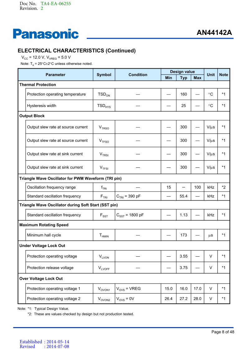
Parameter Symbol Condition Design value
Unit NoteMin Typ Max
Thermal Protection
Protection operating temperature TSDON — — 160 — C *1
Hysteresis width TSDHYS — — 25 — C *1
Output Block
Output slew rate at source current VTRSO — — 300 — V/s *1
Output slew rate at source current VTFSO — — 300 — V/s *1
Output slew rate at sink current VTRSI — — 300 — V/s *1
Output slew rate at sink current VTFSI — — 300 — V/s *1
Triangle Wave Oscillator for PWM Waveform (TRI pin)
Oscillation frequency range fTRI — 15 - 100 kHz *2
Standard oscillation frequency FTRI CTRI = 390 pF — 55.4 — kHz *1
Triangle Wave Oscillator during Soft Start (SST pin)
Standard oscillation frequency FSST CSST = 1800 pF — 1.13 — kHz *1
Maximum Rotating Speed
Minimum hall cycle THMIN — — 173 — s *1
Under Voltage Lock Out
Protection operating voltage VLVON — — 3.55 — V *1
Protection release voltage VLVOFF — — 3.75 — V *1
Over Voltage Lock Out
Protection operating voltage 1 VOVON1 VOVS = VREG 15.0 16.0 17.0 V *1
Protection operating voltage 2 VOVON2 VOVS = 0V 26.4 27.2 28.0 V *1
ELECTRICAL CHARACTERISTICS (Continued)VCC = 12.0 V, VVREG = 5.0 V
Note: Ta = 25C2C unless otherwise noted.
Note: *1: Typical Design Value.
*2: These are values checked by design but not production tested.
Doc No. TA4-EA-06255Revision. 2
Established : 2014-05-14Revised : 2014-07-08
Page 9 of 48
AN44142A
Product Standards
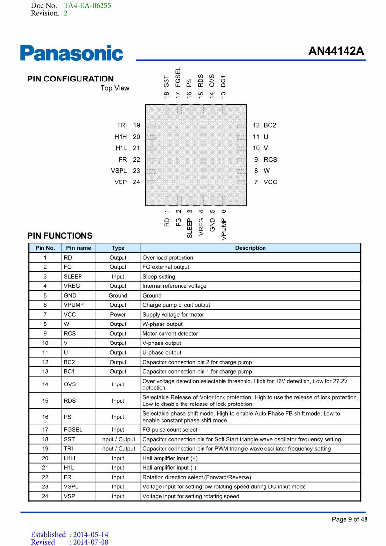
Pin No. Pin name Type Description
1 RD Output Over load protection
2 FG Output FG external output
3 SLEEP Input Sleep setting
4 VREG Output Internal reference voltage
5 GND Ground Ground
6 VPUMP Output Charge pump circuit output
7 VCC Power Supply voltage for motor
8 W Output W-phase output
9 RCS Output Motor current detector
10 V Output V-phase output
11 U Output U-phase output
12 BC2 Output Capacitor connection pin 2 for charge pump
13 BC1 Output Capacitor connection pin 1 for charge pump
14 OVS InputOver voltage detection selectable threshold. High for 16V detection, Low for 27.2V detection
15 RDS InputSelectable Release of Motor lock protection. High to use the release of lock protection. Low to disable the release of lock protection.
16 PS InputSelectable phase shift mode. High to enable Auto Phase FB shift mode. Low to enable constant phase shift mode.
17 FGSEL Input FG pulse count select
18 SST Input / Output Capacitor connection pin for Soft Start triangle wave oscillator frequency setting
19 TRI Input / Output Capacitor connection pin for PWM triangle wave oscillator frequency setting
20 H1H Input Hall amplifier input (+)
21 H1L Input Hall amplifier input (-)
22 FR Input Rotation direction select (Forward/Reverse)
23 VSPL Input Voltage input for setting low rotating speed during DC input mode
24 VSP Input Voltage input for setting rotating speed
Top View
19
20
21
22
23
24
TRI
H1H
H1L
FR
VSPL
VSP
12
11
10
9
8
7
18 17 16 15 14 13
1 2 3 4 5 6
BC2
U
V
RCS
W
VCC
SS
T
FG
SE
L
PS
RD
S
OV
S
BC
1
RD
FG
SLE
EP
VR
EG
GN
D
VP
UM
P
PIN CONFIGURATION
PIN FUNCTIONS
Doc No. TA4-EA-06255Revision. 2
Established : 2014-05-14Revised : 2014-07-08
Page 10 of 48
AN44142A
Product Standards
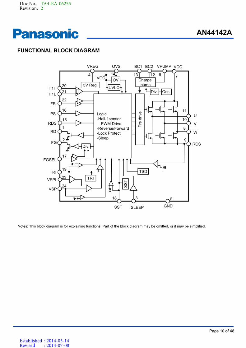
BC2BC1VREG
FG
VPUMP
RD
H1H
H1L
U
V
W
VCC
RCS
FGSEL
612134
21
1
2
17
22FR
7
8
10
11
9
GND
5
TRI
VSP
OVS
14
19
PS16
20
24
5V Reg.
SST
18
SLEEP
3
Pre
driv
e
Div.
Charge pump
VCC
UVLO
OV
Osc.Div.
TSD
RDS15
Logic-Hall-1sensor
PWM Drive-Reverse/Forward-Lock Protect-Sleep
VSPL23 TRI
SS
T
FUNCTIONAL BLOCK DIAGRAM
Notes: This block diagram is for explaining functions. Part of the block diagram may be omitted, or it may be simplified.
Doc No. TA4-EA-06255Revision. 2
Established : 2014-05-14Revised : 2014-07-08
Page 11 of 48
AN44142A
Product Standards
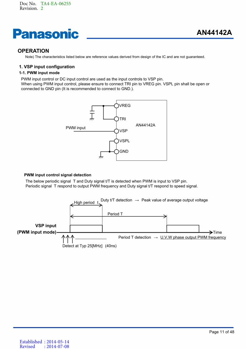
PWM input control or DC input control are used as the input controls to VSP pin.When using PWM input control, please ensure to connect TRI pin to VREG pin. VSPL pin shall be open or connected to GND pin (It is recommended to connect to GND.).
1. VSP input configuration1-1. PWM input mode
PWM input control signal detection
The below periodic signal T and Duty signal t/T is detected when PWM is input to VSP pin.Periodic signal T respond to output PWM frequency and Duty signal t/T respond to speed signal.
VSP input
(PWM input mode)Period T detection → U,V,W phase output PWM frequency
Duty t/T detection → Peak value of average output voltage
Period T
High period t
Detect at Typ 25[MHz] (40ns)
Time
VREG
TRI
VSPL
GND
AN44142APWM input
VSP
OPERATIONNote) The characteristics listed below are reference values derived from design of the IC and are not guaranteed.
Doc No. TA4-EA-06255Revision. 2
Established : 2014-05-14Revised : 2014-07-08
Page 12 of 48
AN44142A
Product Standards
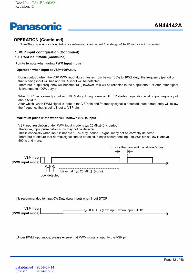
Maximum pulse width when VSP below 100% is input
VSP input resolution under PWM input mode is typ 25MHz(40ns period). Therefore, input pulse below 40ns may not be detected.This is especially when input is near to 100% duty, period T signal many not be correctly detected.Therefore to ensure that normal signal can be detected, please ensure that input to VSP pin at Low is above 500ns and more.
VSP input
(PWM input mode)
Low detected
Ensure that Low width is above 500ns
Points to note when using PWM input mode
It is recommended to input 0% Duty (Low input) when input STOP.
0% Duty (Low input) when input STOP.
Operation when input at VSP=100%duty
During output, when the VSP PWM input duty changes from below 100% to 100% duty, the frequency (period t) that is being input will halt and 100% input will be detected.Therefore, output frequency will become 1/t. (However, this will be reflected in the output about 7t later, after signal is changed to 100% duty.)
When VSP pin is already input with 100% duty during power or SLEEP start-up, operation is at output frequency of about 58kHz.After which, when PWM signal is input to the VSP pin and frequency signal is detected, output frequency will follow the frequency that is being input to VSP pin.
Under PWM input mode, please ensure that PWM signal is input to the VSP pin.
1. VSP input configuration (Continued)1-1. PWM input mode (Continued)
OPERATION (Continued)Note) The characteristics listed below are reference values derived from design of the IC and are not guaranteed.
Detect at Typ 25[MHz] (40ns)
VSP input
(PWM input mode)
Doc No. TA4-EA-06255Revision. 2
Established : 2014-05-14Revised : 2014-07-08
Page 13 of 48
AN44142A
Product Standards
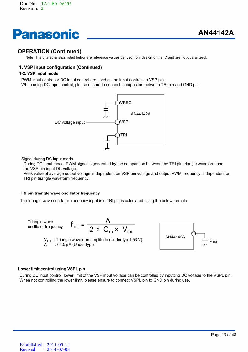
Signal during DC input mode During DC input mode, PWM signal is generated by the comparison between the TRI pin triangle waveform and the VSP pin input DC voltage.Peak value of average output voltage is dependent on VSP pin voltage and output PWM frequency is dependent on TRI pin triangle waveform frequency.
19AN44142A
CTRI
TRI pin triangle wave oscillator frequency
The triangle wave oscillator frequency input into TRI pin is calculated using the below formula.
Triangle wave oscillator frequency
VTRI : Triangle waveform amplitude (Under typ.1.53 V)A : 64.5 A (Under typ.)
f TRI CTRI VTRI
A×2 ×
=
Lower limit control using VSPL pin
During DC input control, lower limit of the VSP input voltage can be controlled by inputting DC voltage to the VSPL pin.When not controlling the lower limit, please ensure to connect VSPL pin to GND pin during use.
VREG
TRI
AN44142A
VSPDC voltage input
OPERATION (Continued)Note) The characteristics listed below are reference values derived from design of the IC and are not guaranteed.
1. VSP input configuration (Continued)1-2. VSP input mode
PWM input control or DC input control are used as the input controls to VSP pin.When using DC input control, please ensure to connect a capacitor between TRI pin and GND pin.
Doc No. TA4-EA-06255Revision. 2
Established : 2014-05-14Revised : 2014-07-08
Page 14 of 48
AN44142A
Product Standards
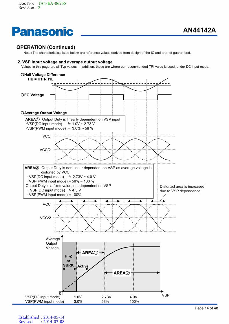
2. VSP input voltage and average output voltageValues in this page are all Typ values. In addition, these are where our recommended TRI value is used, under DC input mode.
Hall Voltage DifferenceHU = H1H-H1L
FG Voltage
Average Output Voltage
VCC
VCC/2
VCC
VCC/2
AREA② Output Duty is non-linear dependent on VSP as average voltage is distorted by VCC
・VSP(DC input mode) ≒ 2.73V ~ 4.0 V・VSP(PWM input mode) = 58% ~ 100 %
Output Duty is a fixed value, not dependent on VSP・ VSP(DC input mode) > 4.3 V・VSP(PWM input mode) = 100%
AREA① Output Duty is linearly dependent on VSP input・VSP(DC input mode) ≒ 1.0V ~ 2.73 V・VSP(PWM input mode) = 3.0% ~ 58 %
Distorted area is increased due to VSP dependence
04.0V100%
AREA②
VSP
Hi-Zor
SBRK Active
VSP(DC input mode)VSP(PWM input mode)
1.0V3.0%
AREA①
2.73V58%
OPERATION (Continued)Note) The characteristics listed below are reference values derived from design of the IC and are not guaranteed.
Average Output Voltage
Doc No. TA4-EA-06255Revision. 2
Established : 2014-05-14Revised : 2014-07-08
Page 15 of 48
AN44142A
Product Standards
20
21
J-10
J-2
H1H
H1L
VREG
H1H
H1L
5V Reg.
J-3
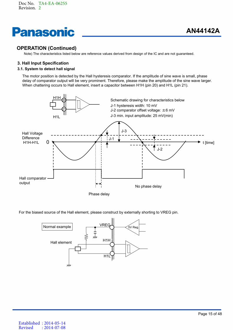
3. Hall Input Specification3.1. System to detect hall signal
OPERATION (Continued)Note) The characteristics listed below are reference values derived from design of the IC and are not guaranteed.
The motor position is detected by the Hall hysteresis comparator. If the amplitude of sine wave is small, phasedelay of comparator output will be very prominent. Therefore, please make the amplitude of the sine wave larger. When chattering occurs to Hall element, insert a capacitor between H1H (pin 20) and H1L (pin 21).
Schematic drawing for characteristics below
J-1 hysteresis width: 10 mV J-2 comparator offset voltage: ±6 mV
J-3 min. input amplitude: 25 mV(min)
Hall Voltage DifferenceH1H-H1L t [time]
Hall comparatoroutput
Phase delay
No phase delay
For the biased source of the Hall element, please construct by externally shorting to VREG pin.
Normal example
Hall element
Doc No. TA4-EA-06255Revision. 2
Established : 2014-05-14Revised : 2014-07-08
Page 16 of 48
AN44142A
Product Standards
FGSEL=HighFG Signal for
1-cycle of Hall sine wave
Hall voltage
FGSEL=Open(Middle)FG Signal for
2-cycles of Hall sine wave
FGSEL=LowFG Signal for
3-cycles ofHall sine wave
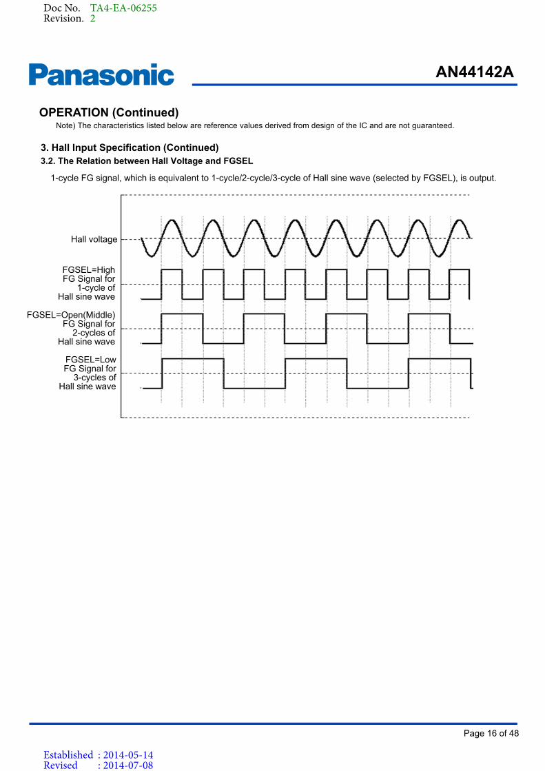
3. Hall Input Specification (Continued)3.2. The Relation between Hall Voltage and FGSEL
OPERATION (Continued)Note) The characteristics listed below are reference values derived from design of the IC and are not guaranteed.
1-cycle FG signal, which is equivalent to 1-cycle/2-cycle/3-cycle of Hall sine wave (selected by FGSEL), is output.
Doc No. TA4-EA-06255Revision. 2
Established : 2014-05-14Revised : 2014-07-08
Page 17 of 48
AN44142A
Product Standards
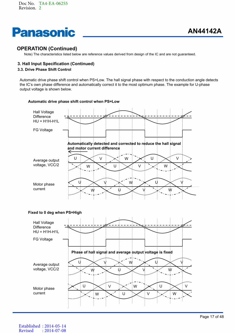
Automatic drive phase shift control when PS=Low. The hall signal phase with respect to the conduction angle detects the IC’s own phase difference and automatically correct it to the most optimum phase. The example for U-phase output voltage is shown below.
U V WW
U VWVU
U V WW
U VWVU
U V WW
U VWVU
U V WW
U VWVU
Automatically detected and corrected to reduce the hall signal and motor current difference
Phase of hall signal and average output voltage is fixed
Automatic drive phase shift control when PS=Low
3. Hall Input Specification (Continued)3.3. Drive Phase Shift Control
OPERATION (Continued)Note) The characteristics listed below are reference values derived from design of the IC and are not guaranteed.
Hall VoltageDifferenceHU = H1H-H1L
FG Voltage
Average output voltage, VCC/2
Motor phasecurrent
Hall VoltageDifferenceHU = H1H-H1L
FG Voltage
Average output voltage, VCC/2
Motor phasecurrent
Fixed to 0 deg when PS=High
Doc No. TA4-EA-06255Revision. 2
Established : 2014-05-14Revised : 2014-07-08
Page 18 of 48
AN44142A
Product Standards
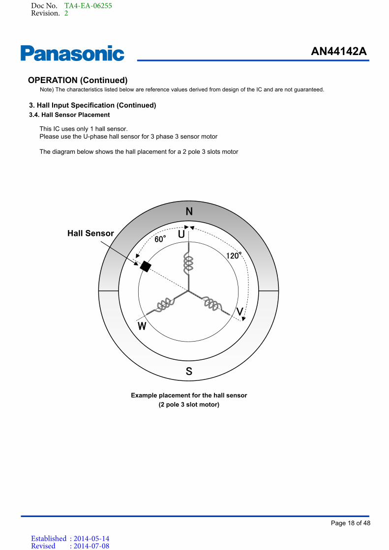
This IC uses only 1 hall sensor.Please use the U-phase hall sensor for 3 phase 3 sensor motor
The diagram below shows the hall placement for a 2 pole 3 slots motor
Example placement for the hall sensor
(2 pole 3 slot motor)
W
V
UHall Sensor
120°
60°
N
S
OPERATION (Continued)Note) The characteristics listed below are reference values derived from design of the IC and are not guaranteed.
3. Hall Input Specification (Continued)3.4. Hall Sensor Placement
Doc No. TA4-EA-06255Revision. 2
Established : 2014-05-14Revised : 2014-07-08
Page 19 of 48
AN44142A
Product Standards
VREG
VSP
Control status
VCC
Hi-ZSine wave
Start-upmode
SLEEP
UVLO release (3.75V)
Low
Circuit initializationabout 2ms
Motor speed
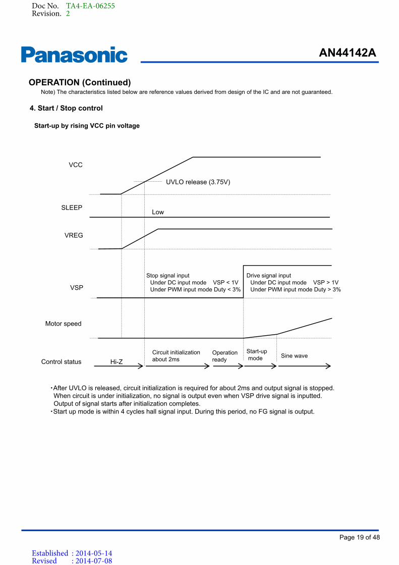
Start-up by rising VCC pin voltage
Operationready
Stop signal inputUnder DC input mode VSP < 1VUnder PWM input mode Duty < 3%
Drive signal inputUnder DC input mode VSP > 1VUnder PWM input mode Duty > 3%
・After UVLO is released, circuit initialization is required for about 2ms and output signal is stopped.When circuit is under initialization, no signal is output even when VSP drive signal is inputted. Output of signal starts after initialization completes.
・Start up mode is within 4 cycles hall signal input. During this period, no FG signal is output.
4. Start / Stop control
OPERATION (Continued)Note) The characteristics listed below are reference values derived from design of the IC and are not guaranteed.
Doc No. TA4-EA-06255Revision. 2
Established : 2014-05-14Revised : 2014-07-08
Page 20 of 48
AN44142A
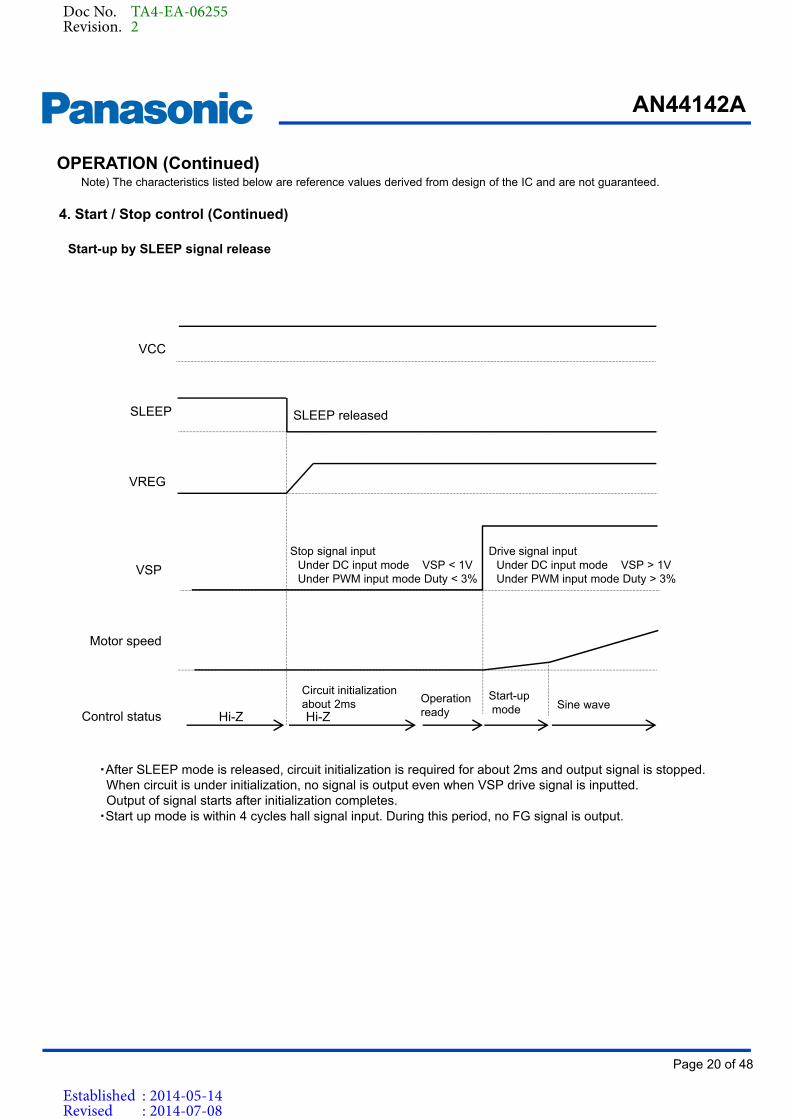
Product Standards
VREG
VSP
VCC
SLEEP SLEEP released
Hi-Z Hi-Z
Start-up by SLEEP signal release
4. Start / Stop control (Continued)
OPERATION (Continued)Note) The characteristics listed below are reference values derived from design of the IC and are not guaranteed.
Stop signal inputUnder DC input mode VSP < 1VUnder PWM input mode Duty < 3%
Drive signal inputUnder DC input mode VSP > 1VUnder PWM input mode Duty > 3%
Control status
Motor speed
Circuit initializationabout 2ms Operation
ready
・After SLEEP mode is released, circuit initialization is required for about 2ms and output signal is stopped.When circuit is under initialization, no signal is output even when VSP drive signal is inputted. Output of signal starts after initialization completes.
・Start up mode is within 4 cycles hall signal input. During this period, no FG signal is output.
Sine wave Start-upmode
Doc No. TA4-EA-06255Revision. 2
Established : 2014-05-14Revised : 2014-07-08

Page 21 of 48
AN44142A
Product Standards
U V
W
W
U
VAverage output voltage
Hall signalH1H-H1L
A C
EB
Start-up sequence Sine wave
The flow chart below illustrates the start-up sequence.
Start-up sequence flow chart
Start-up waveform
Start-up sequence Average output voltage waveforms refer to page 22
D
C C C CC
C C
Start-up sequence
4. Start / Stop control (Continued)
OPERATION (Continued)Note) The characteristics listed below are reference values derived from design of the IC and are not guaranteed.
Doc No. TA4-EA-06255Revision. 2
Established : 2014-05-14Revised : 2014-07-08
Page 22 of 48
AN44142A
Product Standards
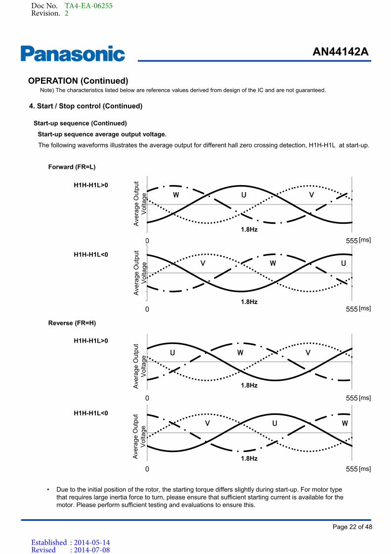
Start-up sequence average output voltage.
Forward (FR=L)
-1.5-1
-0.50
0.51
1.5
0 555
V U W
-1.5-1
-0.50
0.51
1.5
0 555
U W V
Reverse (FR=H)
[ms]
[ms]
[ms]
[ms]
The following waveforms illustrates the average output for different hall zero crossing detection, H1H-H1L at start-up.
-1.5-1
-0.50
0.51
1.5
0 555
W U V
H1H-H1L>0
H1H-H1L<0
H1H-H1L>0
1.8Hz
1.8Hz
1.8Hz
1.8Hz
Ave
rage
Out
put
Vol
tage
-1.5-1
-0.50
0.51
1.5
0 555
V W U
Ave
rage
Out
put
Vol
tage
Ave
rage
Out
put
Vol
tage
Ave
rage
Out
put
Vol
tage
• Due to the initial position of the rotor, the starting torque differs slightly during start-up. For motor type that requires large inertia force to turn, please ensure that sufficient starting current is available for the motor. Please perform sufficient testing and evaluations to ensure this.
H1H-H1L<0
Start-up sequence (Continued)
4. Start / Stop control (Continued)
OPERATION (Continued)Note) The characteristics listed below are reference values derived from design of the IC and are not guaranteed.
Doc No. TA4-EA-06255Revision. 2
Established : 2014-05-14Revised : 2014-07-08
Page 23 of 48
AN44142A
Product Standards
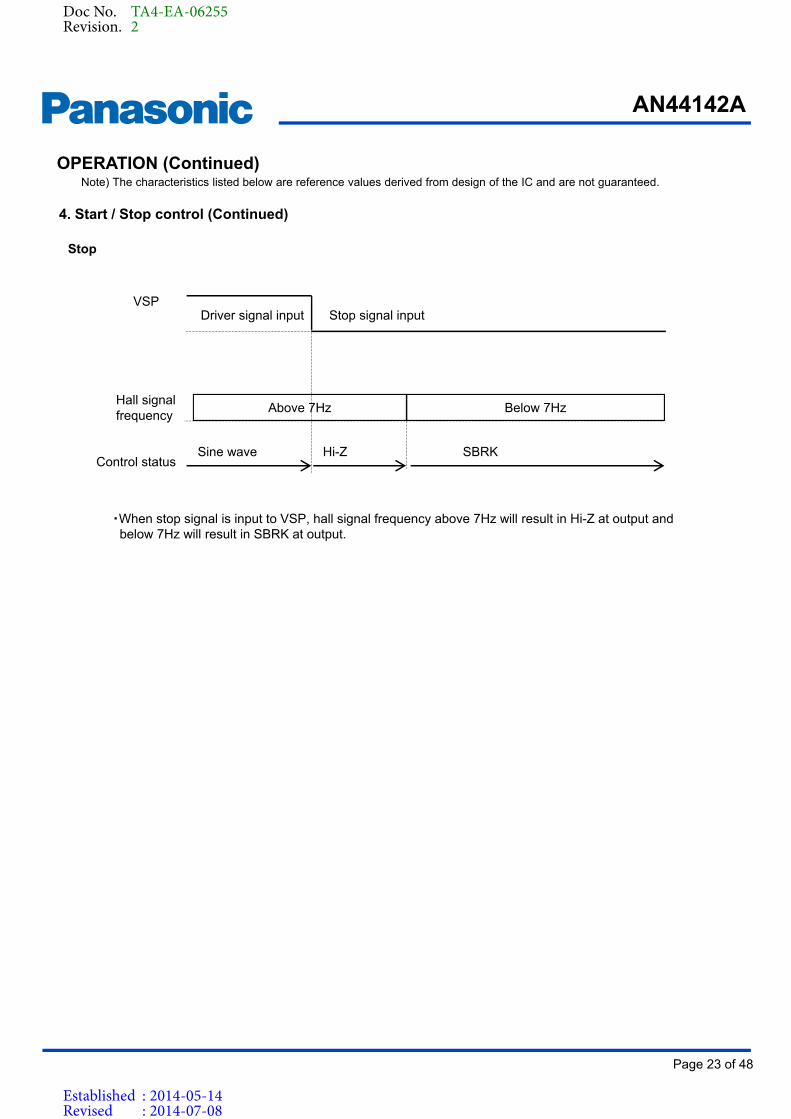
VSP
Hall signalfrequency
Control status
Stop signal inputDriver signal input
Sine wave
Above 7Hz Below 7Hz
Hi-Z SBRK
・When stop signal is input to VSP, hall signal frequency above 7Hz will result in Hi-Z at output and below 7Hz will result in SBRK at output.
Stop
4. Start / Stop control (Continued)
OPERATION (Continued)Note) The characteristics listed below are reference values derived from design of the IC and are not guaranteed.
Doc No. TA4-EA-06255Revision. 2
Established : 2014-05-14Revised : 2014-07-08
Page 24 of 48
AN44142A
Product Standards
19
24
SST
VSP
Time
0 Time
TRI
Pulseconversion
circuit18
5. Soft Start Function and PWM Specification
OPERATION (Continued)Note) The characteristics listed below are reference values derived from design of the IC and are not guaranteed.
By connecting a capacitor to the SST pin, soft start control is performed by the start-up mode conditions during the mode transition. The period for soft start control is determined by the formula shown on the next page. When soft start control is not required, ensure to connect SST pin to VREG pin.
PWM input
DC input
Change to PWM
PWM Dutycounter circuit
SST pulsecounter circuit
Count data comparison
circuit
Dutyenabled
Count data is compared andlower one is used as duty
Below shows the correlation timing chart of count data and PWM enabled duty for VSP and SST.
PWM Dutycount data
SST pulsecount data
Count data is comparedand lower one is used as duty
Cou
nt d
ata
PW
M e
nabl
ed d
uty
sign
al
Time elapsedTPASS [s]
SST enabled period
About 1msWaiting time for SST oscillator to achieve stable output
Start
・Notes on the use of the soft-start function.With the increase in soft-start time, the motor current will also increase slowly . Therefore if the soft-start timing is too long, it will result in the motor not having enough starting torque and lock protection detection will be triggered if soft start timing is more than 0.5s (typ). This will cause the motor to be unable to start. Please evaluate and check this condition thoroughly when using this function.
Doc No. TA4-EA-06255Revision. 2
Established : 2014-05-14Revised : 2014-07-08

Page 25 of 48
AN44142A
Product Standards
×=PWM duty
TPASS TOSC
TSST TPWM×
×=TPASS TOSC
TSSTTPWM×D
Under DC input, VVSP=1V~4V
18AN44142A
CSST
Triangle wave oscillator frequency
VSST : Triangle waveform amplitude (At typ. 1 V)A : Current flowing in/out SST pin (At typ. 4 A)
fSST CSST VSST
A×2 ×
=
5. Soft Start Function and PWM Specification (Continued)
OPERATION (Continued)Note) The characteristics listed below are reference values derived from design of the IC and are not guaranteed.
The PWM enabled duty reflected in the output, at the time elapsed TPASS within the SST enabled timing is determined by the below formula:
TPWM : Input PWM cycle [s]TOSC : Oscillation cycle of internal oscillator
40*10-9 [s]TSST : SST triangle wave oscillation cycle[s]TPASS : Time elapsed [s]
TPASS at the end of the SST timing can be determined by the below formula:
D : Input PWM duty [%]
Input PWM duty during the DC input can be determined by the below formula:
The triangle wave oscillator frequency output by SST pin is determined by the below formula. Soft Start timing is generated by comparing the VSP pin input PWM frequency and this triangle waveform frequency.
( )= ×D973 VVSP
883
- × 0.01
Doc No. TA4-EA-06255Revision. 2
Established : 2014-05-14Revised : 2014-07-08
Page 26 of 48
AN44142A
Product Standards
Forward (FR = L)
U V WW
U VWVU
Reverse (FR = H)
W V U W V
U W V U
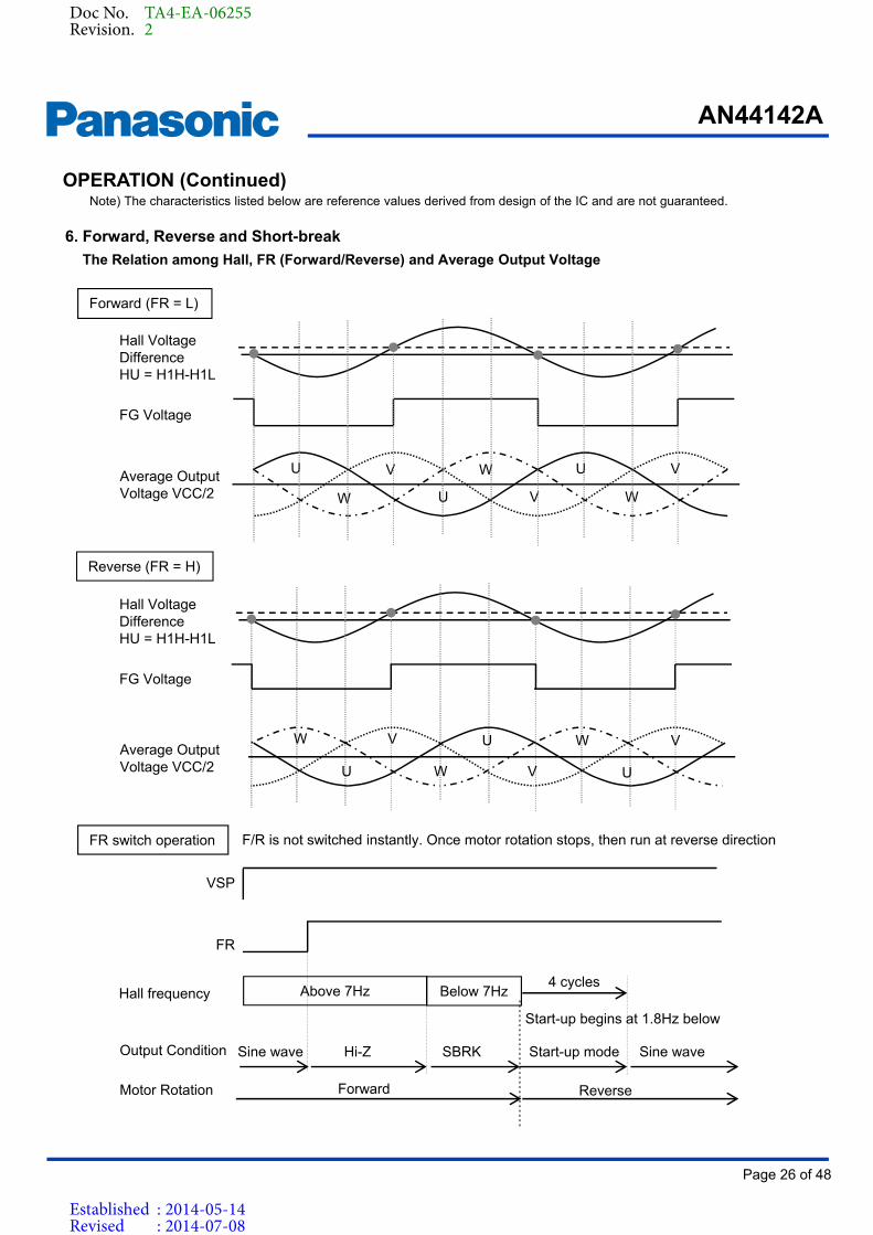
FR switch operation
FR
Hall frequency
VSP
Forward Reverse
Start-up begins at 1.8Hz below
Above 7Hz Below 7Hz4 cycles
Sine wave Hi-Z SBRK Start-up mode Sine wave
OPERATION (Continued)Note) The characteristics listed below are reference values derived from design of the IC and are not guaranteed.
6. Forward, Reverse and Short-break
The Relation among Hall, FR (Forward/Reverse) and Average Output Voltage
Hall VoltageDifferenceHU = H1H-H1L
Average OutputVoltage VCC/2
FG Voltage
Hall VoltageDifferenceHU = H1H-H1L
Average OutputVoltage VCC/2
FG Voltage
Output Condition
Motor Rotation
F/R is not switched instantly. Once motor rotation stops, then run at reverse direction
Doc No. TA4-EA-06255Revision. 2
Established : 2014-05-14Revised : 2014-07-08
Page 27 of 48
AN44142A
Product Standards
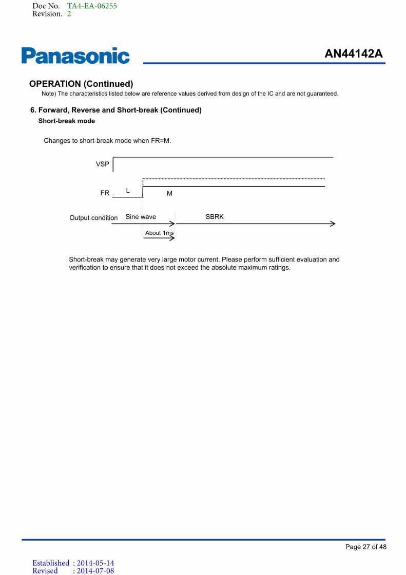
Changes to short-break mode when FR=M.
FR
Output condition
VSP
Sine wave
About 1ms
SBRK
L M
Short-break may generate very large motor current. Please perform sufficient evaluation and verification to ensure that it does not exceed the absolute maximum ratings.
OPERATION (Continued)Note) The characteristics listed below are reference values derived from design of the IC and are not guaranteed.
6. Forward, Reverse and Short-break (Continued)
Short-break mode
Doc No. TA4-EA-06255Revision. 2
Established : 2014-05-14Revised : 2014-07-08
Page 28 of 48
AN44142A
Product Standards
OPERATION (Continued)Note) The characteristics listed below are reference values derived from design of the IC and are not guaranteed.
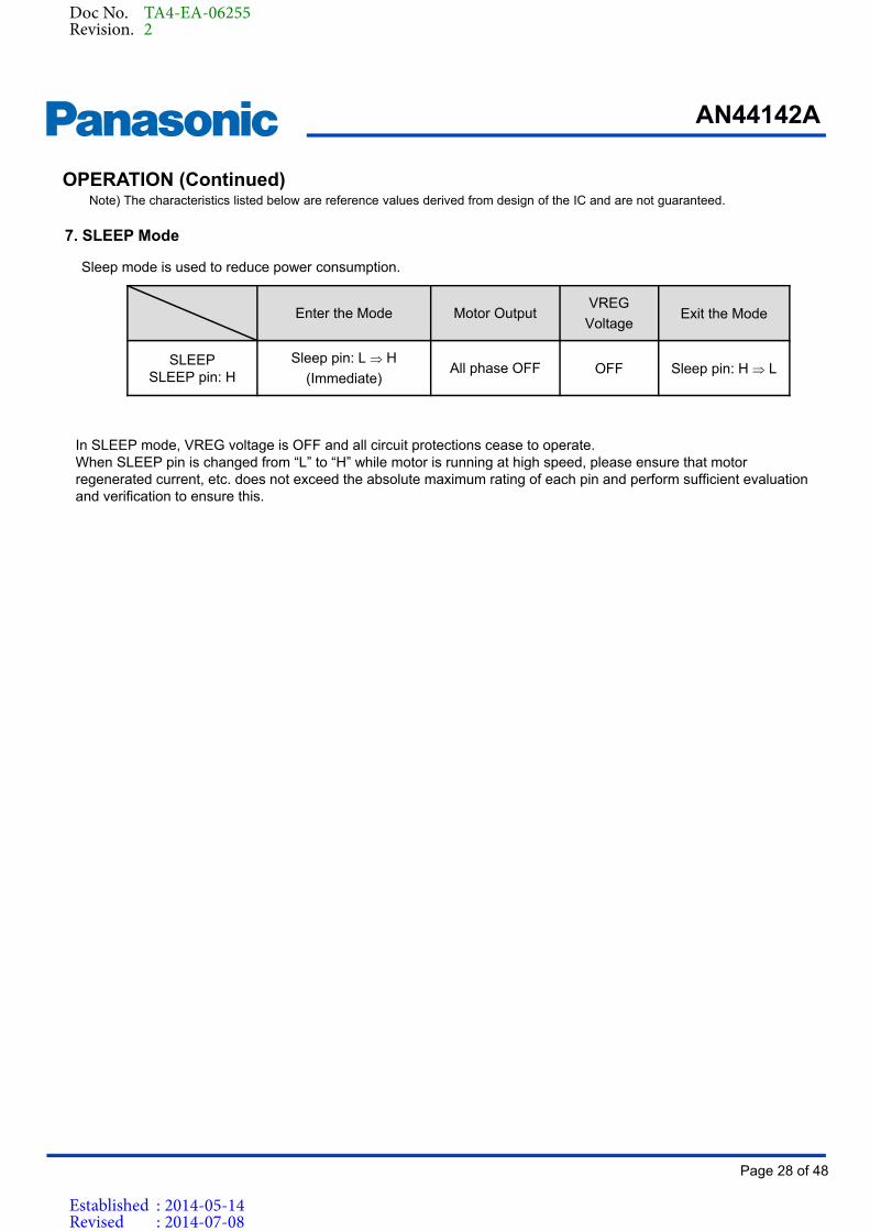
7. SLEEP Mode
Enter the Mode Motor OutputVREG
VoltageExit the Mode
SLEEPSLEEP pin: H
Sleep pin: L H
(Immediate)All phase OFF OFF Sleep pin: H L
Sleep mode is used to reduce power consumption.
In SLEEP mode, VREG voltage is OFF and all circuit protections cease to operate.When SLEEP pin is changed from “L” to “H” while motor is running at high speed, please ensure that motor regenerated current, etc. does not exceed the absolute maximum rating of each pin and perform sufficient evaluation and verification to ensure this.
Doc No. TA4-EA-06255Revision. 2
Established : 2014-05-14Revised : 2014-07-08
Page 29 of 48
AN44142A
Product Standards
L HH
SBRK
H L H
SBRK
Active Active
Active Active
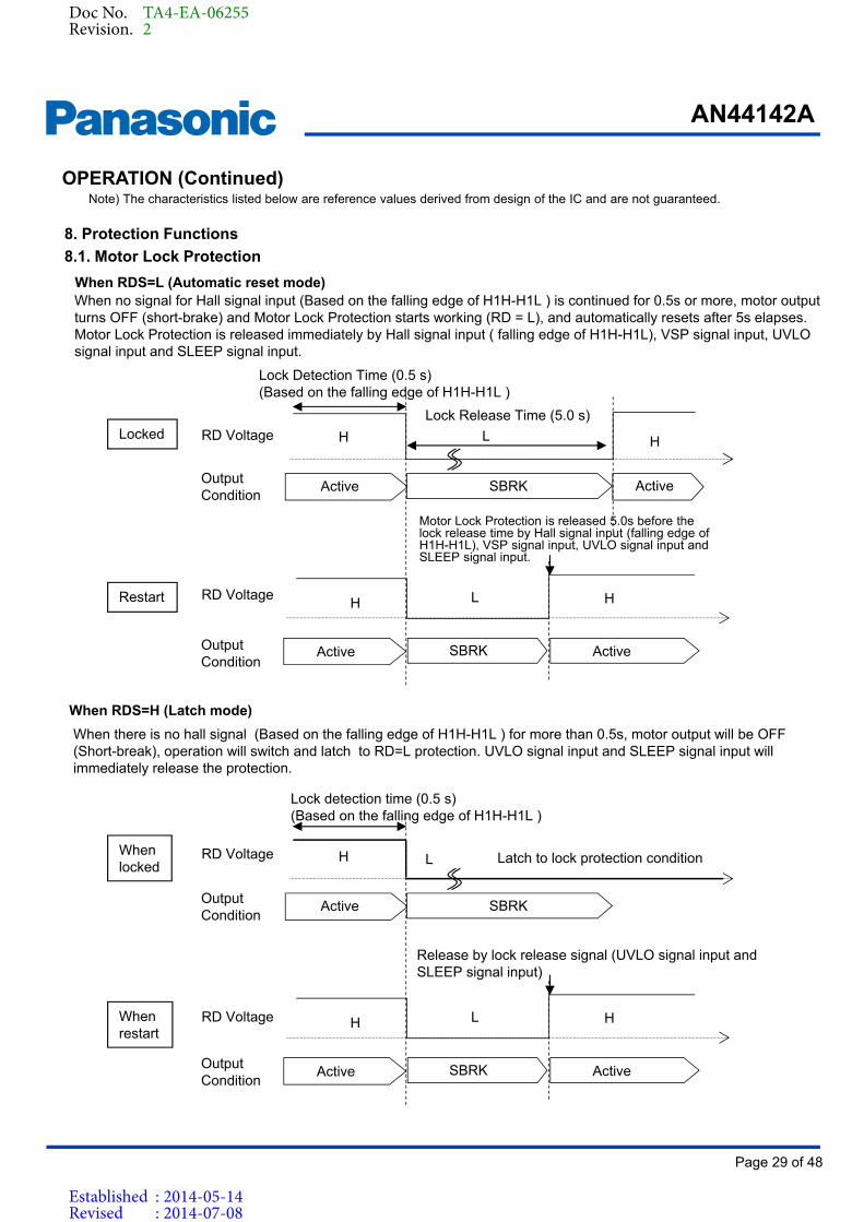
When RDS=L (Automatic reset mode)
Lock detection time (0.5 s)(Based on the falling edge of H1H-H1L )
Latch to lock protection conditionLWhenlocked
H
SBRK
Whenrestart
H L H
SBRK
When there is no hall signal (Based on the falling edge of H1H-H1L ) for more than 0.5s, motor output will be OFF (Short-break), operation will switch and latch to RD=L protection. UVLO signal input and SLEEP signal input will immediately release the protection.
Active
Active Active
When RDS=H (Latch mode)
Release by lock release signal (UVLO signal input and SLEEP signal input)
OPERATION (Continued)Note) The characteristics listed below are reference values derived from design of the IC and are not guaranteed.
8. Protection Functions
8.1. Motor Lock Protection
When no signal for Hall signal input (Based on the falling edge of H1H-H1L ) is continued for 0.5s or more, motor output turns OFF (short-brake) and Motor Lock Protection starts working (RD = L), and automatically resets after 5s elapses. Motor Lock Protection is released immediately by Hall signal input ( falling edge of H1H-H1L), VSP signal input, UVLO signal input and SLEEP signal input.
Lock Detection Time (0.5 s)(Based on the falling edge of H1H-H1L )
Lock Release Time (5.0 s)
RD Voltage
OutputCondition
Locked
Motor Lock Protection is released 5.0s before the lock release time by Hall signal input (falling edge of H1H-H1L), VSP signal input, UVLO signal input and SLEEP signal input.
Restart RD Voltage
OutputCondition
RD Voltage
OutputCondition
RD Voltage
OutputCondition
Doc No. TA4-EA-06255Revision. 2
Established : 2014-05-14Revised : 2014-07-08
Page 30 of 48
AN44142A
Product Standards
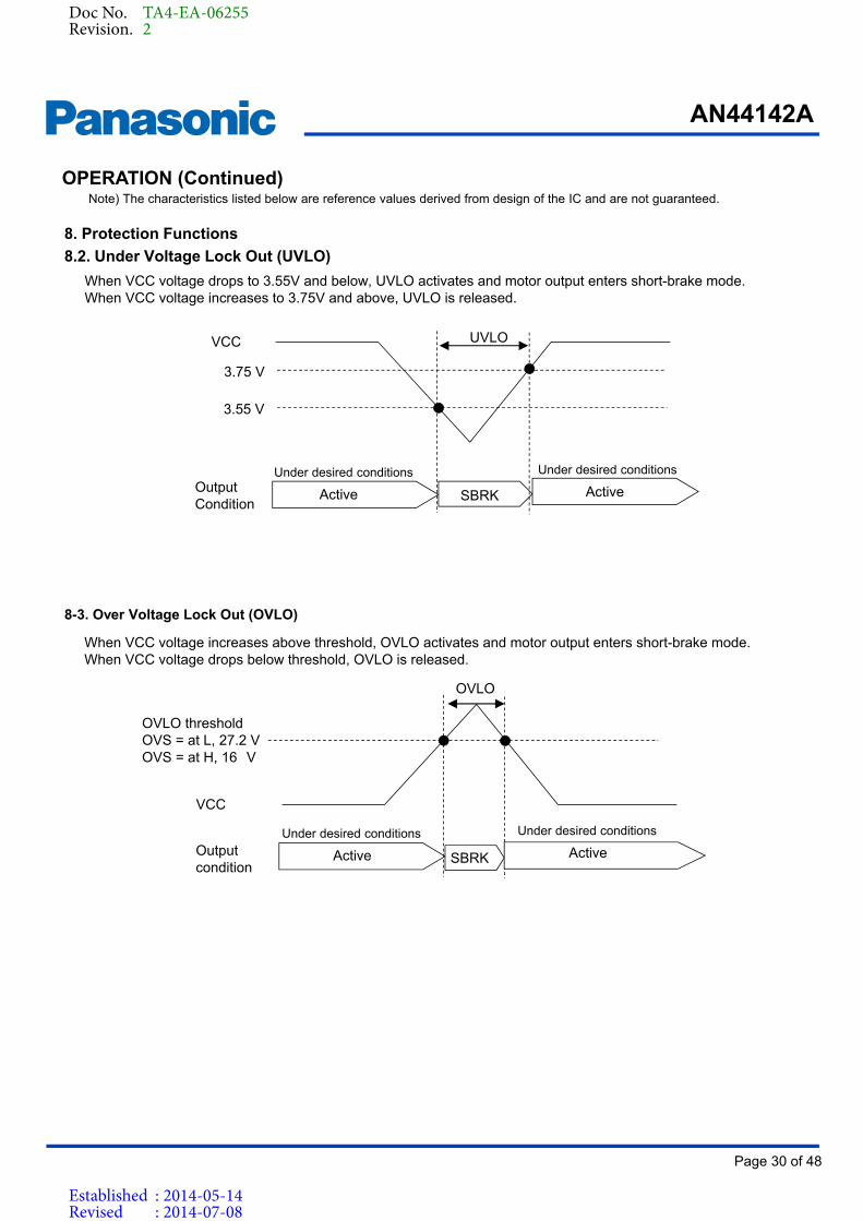
VCC
3.55 V
SBRK
UVLO
8-3. Over Voltage Lock Out (OVLO)
VCC
OVLO thresholdOVS = at L, 27.2 VOVS = at H, 16 V
SBRK
OVLO
OutputCondition
When VCC voltage increases above threshold, OVLO activates and motor output enters short-brake mode.When VCC voltage drops below threshold, OVLO is released.
Outputcondition
Under desired conditions
Active
Under desired conditions
Active
Under desired conditions
Active
Under desired conditions
Active
When VCC voltage drops to 3.55V and below, UVLO activates and motor output enters short-brake mode.When VCC voltage increases to 3.75V and above, UVLO is released.
3.75 V
OPERATION (Continued)Note) The characteristics listed below are reference values derived from design of the IC and are not guaranteed.
8. Protection Functions
8.2. Under Voltage Lock Out (UVLO)
Doc No. TA4-EA-06255Revision. 2
Established : 2014-05-14Revised : 2014-07-08
Page 31 of 48
AN44142A
Product Standards
8-5. Thermal Shut Down (TSD)
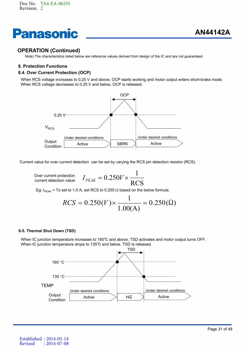
VRCS
0.25 V
SBRK
OCP
TEMP
160 C
HiZ
TSD
135 C
OutputCondition
OutputCondition
Under desired conditions
Active
Under desired conditions
Active
Under desired conditions
Active
Under desired conditions
Active
RCS1250.0 VIPEAK
)(250.01.00(A)1)(250.0 Ω VRCS
Current value for over current detection can be set by varying the RCS pin detection resistor (RCS).
Eg: IPEAK = To set to 1.0 A, set RCS to 0.250 based on the below formula.
Over current protectioncurrent detection value
OPERATION (Continued)Note) The characteristics listed below are reference values derived from design of the IC and are not guaranteed.
8. Protection Functions
8.4. Over Current Protection (OCP)
When RCS voltage increases to 0.25 V and above, OCP starts working and motor output enters short-brake mode.When RCS voltage decreases to 0.25 V and below, OCP is released.
When IC junction temperature increases to 160 and above, TSD activates and motor output turns OFF. When IC junction temperature drops to 135 and below, TSD is released.
Doc No. TA4-EA-06255Revision. 2
Established : 2014-05-14Revised : 2014-07-08
Page 32 of 48
AN44142A
Product Standards
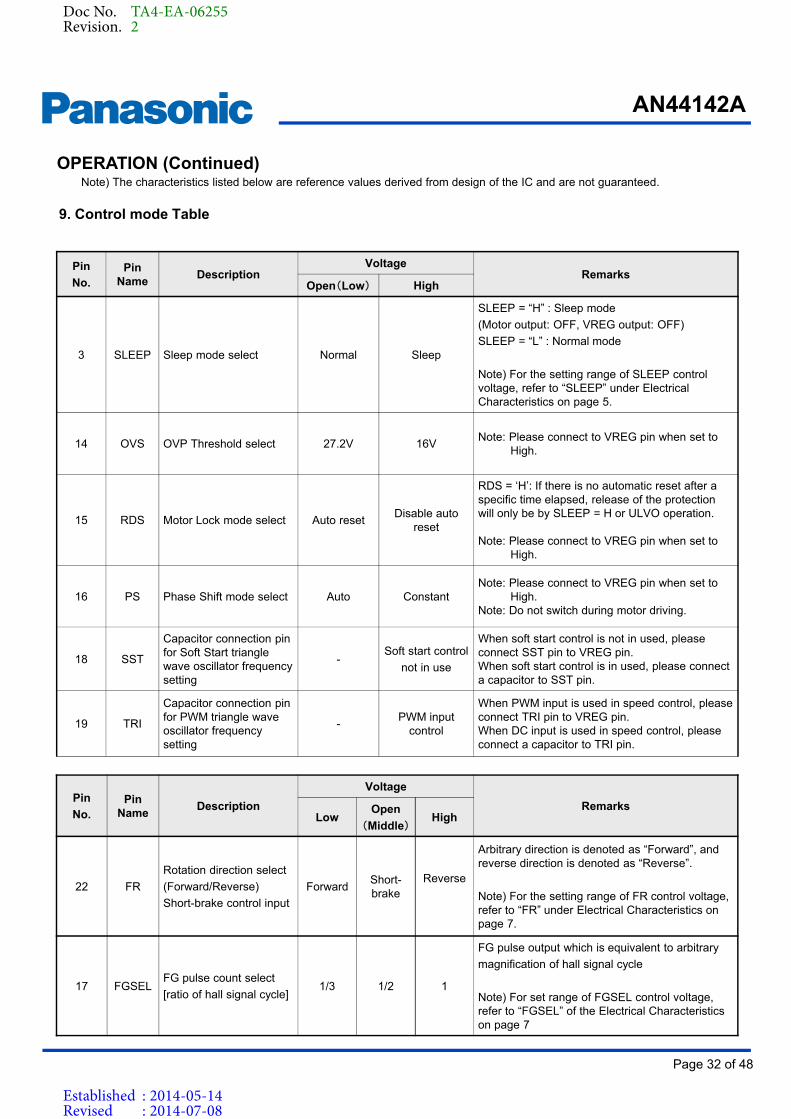
OPERATION (Continued)Note) The characteristics listed below are reference values derived from design of the IC and are not guaranteed.
Pin
No.Pin
NameDescription
VoltageRemarks
Open(Low) High
3 SLEEP Sleep mode select Normal Sleep
SLEEP = “H” : Sleep mode
(Motor output: OFF, VREG output: OFF)
SLEEP = “L” : Normal mode
Note) For the setting range of SLEEP control voltage, refer to “SLEEP” under Electrical Characteristics on page 5.
14 OVS OVP Threshold select 27.2V 16VNote: Please connect to VREG pin when set to
High.
15 RDS Motor Lock mode select Auto resetDisable auto
reset
RDS = ‘H’: If there is no automatic reset after a specific time elapsed, release of the protection will only be by SLEEP = H or ULVO operation.
Note: Please connect to VREG pin when set to High.
16 PS Phase Shift mode select Auto ConstantNote: Please connect to VREG pin when set to
High.Note: Do not switch during motor driving.
18 SST
Capacitor connection pin for Soft Start triangle wave oscillator frequency setting
-Soft start control
not in use
When soft start control is not in used, please connect SST pin to VREG pin.When soft start control is in used, please connect a capacitor to SST pin.
19 TRI
Capacitor connection pin for PWM triangle wave oscillator frequency setting
-PWM input
control
When PWM input is used in speed control, please connect TRI pin to VREG pin.When DC input is used in speed control, please connect a capacitor to TRI pin.
Pin
No.Pin
NameDescription
Voltage
RemarksLow
Open
(Middle)High
22 FR
Rotation direction select
(Forward/Reverse)
Short-brake control input
ForwardShort-brake
Reverse
Arbitrary direction is denoted as “Forward”, and reverse direction is denoted as “Reverse”.
Note) For the setting range of FR control voltage, refer to “FR” under Electrical Characteristics on page 7.
17 FGSELFG pulse count select
[ratio of hall signal cycle]1/3 1/2 1
FG pulse output which is equivalent to arbitrary
magnification of hall signal cycle
Note) For set range of FGSEL control voltage, refer to “FGSEL” of the Electrical Characteristics on page 7
9. Control mode Table
Doc No. TA4-EA-06255Revision. 2
Established : 2014-05-14Revised : 2014-07-08
Page 33 of 48
AN44142A
Product Standards
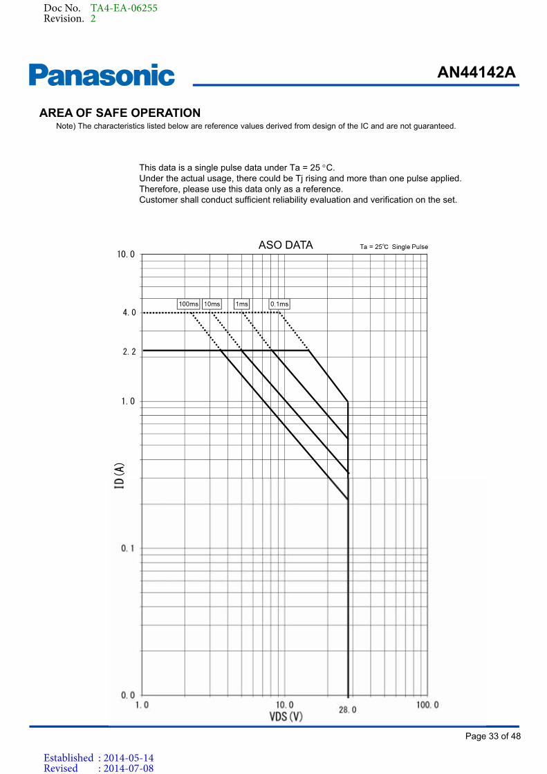
This data is a single pulse data under Ta = 25 C.Under the actual usage, there could be Tj rising and more than one pulse applied.Therefore, please use this data only as a reference.Customer shall conduct sufficient reliability evaluation and verification on the set.
AREA OF SAFE OPERATIONNote) The characteristics listed below are reference values derived from design of the IC and are not guaranteed.
Doc No. TA4-EA-06255Revision. 2
Established : 2014-05-14Revised : 2014-07-08
Page 34 of 48
AN44142A
Product Standards
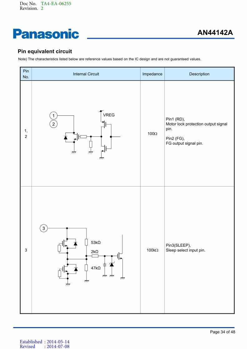
Pin equivalent circuitNote) The characteristics listed below are reference values based on the IC design and are not guaranteed values.
Pin
No.Internal Circuit Impedance Description
1,
2100
Pin1 (RD),Motor lock protection output signal pin.
Pin2 (FG),FG output signal pin.
3 100kPin3(SLEEP),Sleep select input pin.
1 VREG
3
2
53kΩ
47kΩ
2kΩ
Doc No. TA4-EA-06255Revision. 2
Established : 2014-05-14Revised : 2014-07-08
Page 35 of 48
AN44142A
Product Standards
Pin
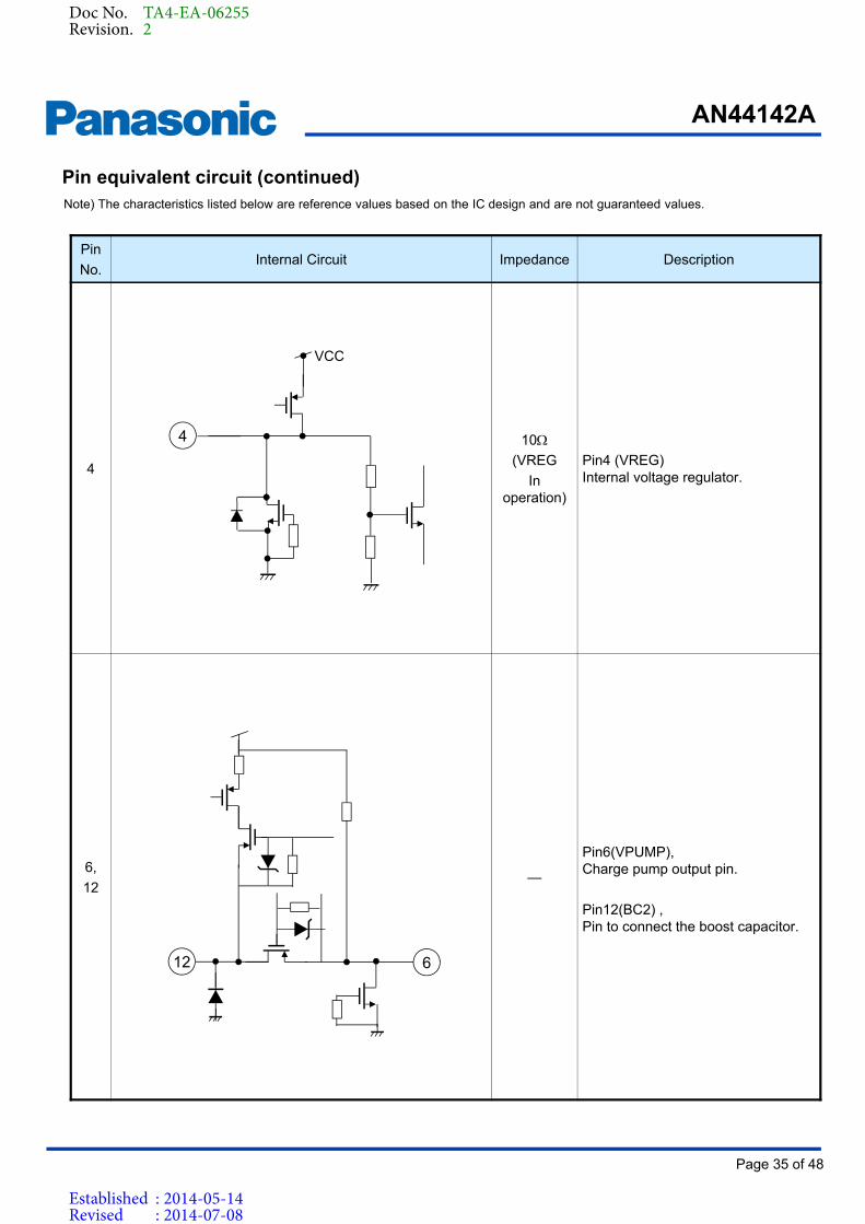
No.Internal Circuit Impedance Description
4
10(VREG
In operation)
Pin4 (VREG)Internal voltage regulator.
6,
12—
Pin6(VPUMP),Charge pump output pin.
Pin12(BC2) ,Pin to connect the boost capacitor.
12 6
4
VCC
Pin equivalent circuit (continued)Note) The characteristics listed below are reference values based on the IC design and are not guaranteed values.
Doc No. TA4-EA-06255Revision. 2
Established : 2014-05-14Revised : 2014-07-08
Page 36 of 48
AN44142A
Product Standards
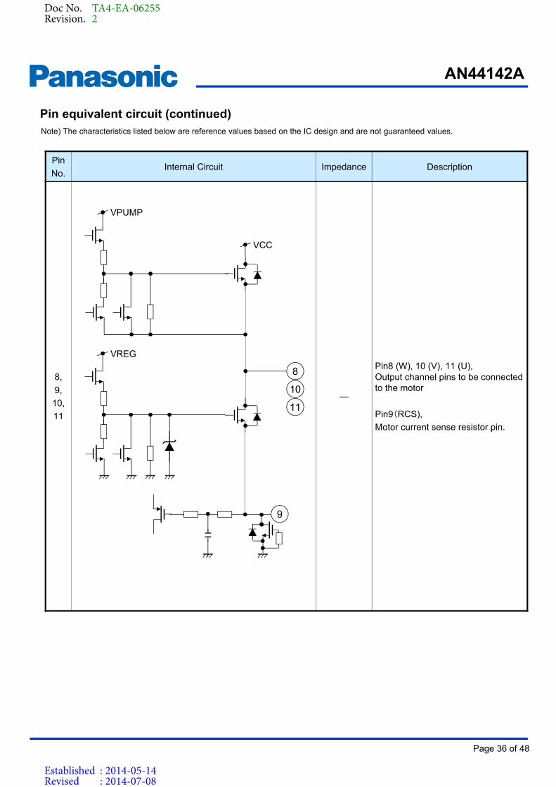
Pin
No.Internal Circuit Impedance Description
8,
9,
10,
11
—
Pin8 (W), 10 (V), 11 (U),Output channel pins to be connected to the motor
Pin9(RCS),
Motor current sense resistor pin.
9
8
10
11
VCC
VPUMP
VREG
Pin equivalent circuit (continued)Note) The characteristics listed below are reference values based on the IC design and are not guaranteed values.
Doc No. TA4-EA-06255Revision. 2
Established : 2014-05-14Revised : 2014-07-08
Page 37 of 48
AN44142A
Product Standards
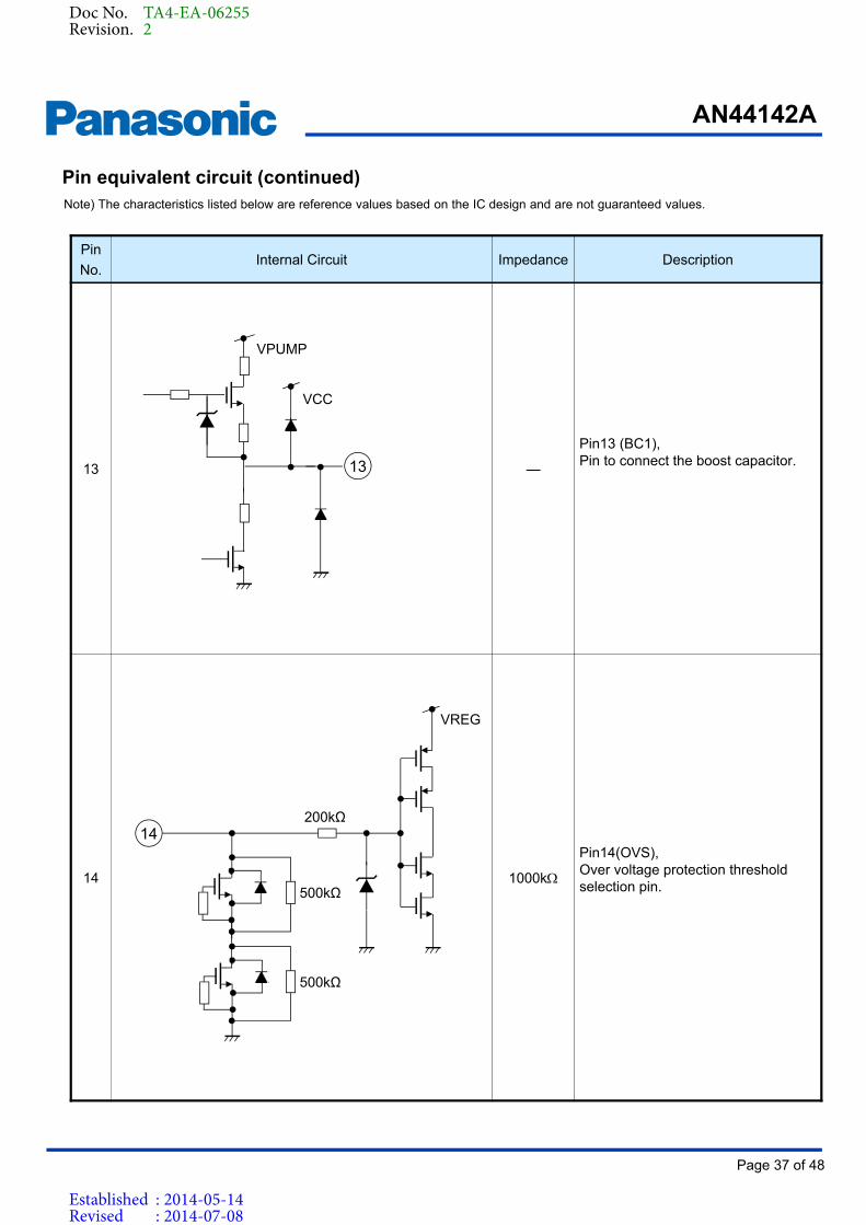
Pin
No.Internal Circuit Impedance Description
13 —
Pin13 (BC1),Pin to connect the boost capacitor.
14 1000k
Pin14(OVS),Over voltage protection threshold selection pin.
13
VPUMP
VCC
14
VREG
500kΩ
500kΩ
200kΩ
Pin equivalent circuit (continued)Note) The characteristics listed below are reference values based on the IC design and are not guaranteed values.
Doc No. TA4-EA-06255Revision. 2
Established : 2014-05-14Revised : 2014-07-08
Page 38 of 48
AN44142A
Product Standards
Pin
No.Internal Circuit Impedance Description
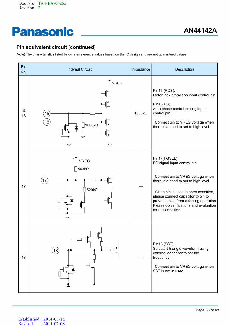
15,
161000k
Pin15 (RDS),Motor lock protection input control pin.
Pin16(PS) ,Auto phase control setting input control pin.
・Connect pin to VREG voltage when there is a need to set to high level.
17 —
Pin17(FGSEL),FG signal input control pin.
・Connect pin to VREG voltage when there is a need to set to high level.
・When pin is used in open condition, please connect capacitor to pin to prevent noise from affecting operation. Please do verifications and evaluation for this condition.
18 —
Pin18 (SST),Soft start triangle waveform using external capacitor to set the frequency.
・Connect pin to VREG voltage when SST is not in used.
17
VREG
18
15
VREG
161000kΩ
563kΩ
520kΩ
Pin equivalent circuit (continued)Note) The characteristics listed below are reference values based on the IC design and are not guaranteed values.
Doc No. TA4-EA-06255Revision. 2
Established : 2014-05-14Revised : 2014-07-08
Page 39 of 48
AN44142A
Product Standards
Pin
No.Internal Circuit Impedance Description
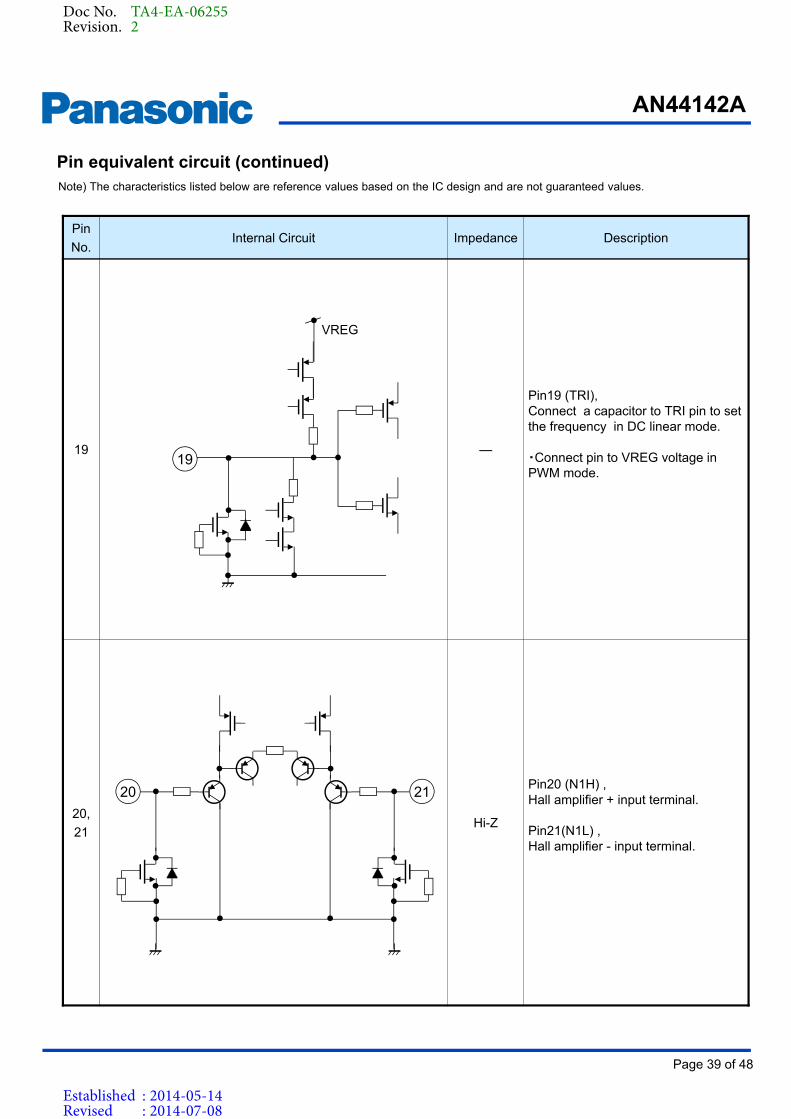
19 —
Pin19 (TRI),Connect a capacitor to TRI pin to set the frequency in DC linear mode.
・Connect pin to VREG voltage in PWM mode.
20,
21Hi-Z
Pin20 (N1H) ,Hall amplifier + input terminal.
Pin21(N1L) ,Hall amplifier - input terminal.
19
VREG
20 21
Pin equivalent circuit (continued)Note) The characteristics listed below are reference values based on the IC design and are not guaranteed values.
Doc No. TA4-EA-06255Revision. 2
Established : 2014-05-14Revised : 2014-07-08
Page 40 of 48
AN44142A
Product Standards
Pin
No.Internal Circuit Impedance Description
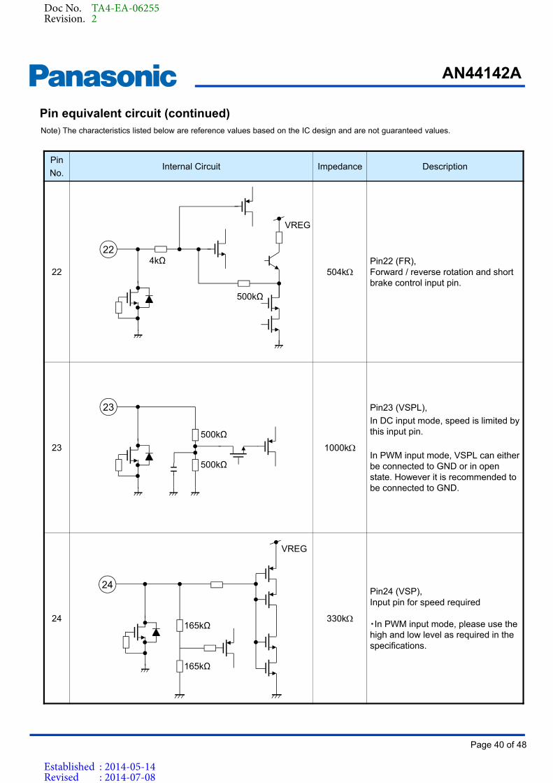
22 504kPin22 (FR),Forward / reverse rotation and short brake control input pin.
23 1000k
Pin23 (VSPL),
In DC input mode, speed is limited by this input pin.
In PWM input mode, VSPL can either be connected to GND or in open state. However it is recommended to be connected to GND.
24 330k
Pin24 (VSP),Input pin for speed required
・In PWM input mode, please use the high and low level as required in the specifications.
24
22
VREG
23
VREG
4kΩ
500kΩ
500kΩ
165kΩ
165kΩ
Pin equivalent circuit (continued)Note) The characteristics listed below are reference values based on the IC design and are not guaranteed values.
500kΩ
Doc No. TA4-EA-06255Revision. 2
Established : 2014-05-14Revised : 2014-07-08

Page 41 of 48
AN44142A
Product Standards
Unit: mmPackage code: HQFN024-A-0404AZ
PACKAGE INFORMATION
Outline Drawing
Lead Finish Method : Pd Plating
Lead Material : Cu Alloy
Body Material : Br/Sb Free Epoxy Resin
Doc No. TA4-EA-06255Revision. 2
Established : 2014-05-14Revised : 2014-07-08
Page 42 of 48
AN44142A
Product Standards
PACKAGE INFORMATION (Continued)
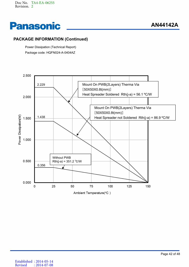
Power Dissipation (Technical Report)
Package code: HQFN024-A-0404AZ
Mount On PWB(2Layers) Therma Via
[50X50X0.8t(mm)]
Heat Spreader not Soldered Rth(j-a) = 86.9 ºC/W
Mount On PWB(2Layers) Therma Via
[50X50X0.8t(mm)]
Heat Spreader Soldered Rth(j-a) = 56.1 ºC/W
Without PWBRth(j-a) = 351.2 /W
2.229
1.438
0.356
Doc No. TA4-EA-06255Revision. 2
Established : 2014-05-14Revised : 2014-07-08
Page 43 of 48
AN44142A
Product Standards
PACKAGE INFORMATION (Continued)
Power Dissipation (Supplementary Explanation)
[Supplementary information of PWB to be used for measurement]The supplement of PWB information for Power Dissipation data (Technical Report)are shown below.
[Experiment environment]Power Dissipation(Technical Report)is a result in the experiment environment of SEMI standard conformity.
(Ambient air temperature (Ta) is 25 degrees C)
Package
Semiconductor element
Rth(j-c)
Rth(c-a)
Rth(j-a)
Ta
Tc
Tj
PWB
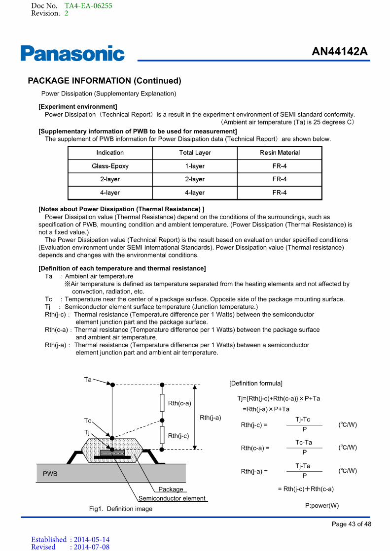
[Definition of each temperature and thermal resistance]Ta :Ambient air temperature
※Air temperature is defined as temperature separated from the heating elements and not affected byconvection, radiation, etc.
Tc :Temperature near the center of a package surface. Opposite side of the package mounting surface. Tj : Semiconductor element surface temperature (Junction temperature.)Rth(j-c): Thermal resistance (Temperature difference per 1 Watts) between the semiconductor
element junction part and the package surface.Rth(c-a):Thermal resistance (Temperature difference per 1 Watts) between the package surface
and ambient air temperature.Rth(j-a): Thermal resistance (Temperature difference per 1 Watts) between a semiconductor
element junction part and ambient air temperature.
[Notes about Power Dissipation (Thermal Resistance) ]Power Dissipation value (Thermal Resistance) depend on the conditions of the surroundings, such as
specification of PWB, mounting condition and ambient temperature. (Power Dissipation (Thermal Resistance) is not a fixed value.)
The Power Dissipation value (Technical Report) is the result based on evaluation under specified conditions (Evaluation environment under SEMI International Standards). Power Dissipation value (Thermal resistance) depends and changes with the environmental conditions.
[Definition formula]
Rth(j-c) =Tj-Tc
P
Rth(c-a) =Tc-Ta
P
Rth(j-a) =Tj-Ta
P(/W)
(/W)
(/W)
Tj=Rth(j-c)+Rth(c-a)×P+Ta
=Rth(j-a)×P+Ta
P:power(W)Fig1. Definition image
= Rth(j-c)+Rth(c-a)
Doc No. TA4-EA-06255Revision. 2
Established : 2014-05-14Revised : 2014-07-08
Page 44 of 48
AN44142A
Product Standards
1. When using the IC for new models, verify the safety including the long-term reliability for each product.
2. When the application system is designed by using this IC, please confirm the notes in this book. Please read the notes to descriptions and the usage notes in the book.
3. This IC is intended to be used for general electronic equipment.Consult our sales staff in advance for information on the following applications: Special applications in which exceptional quality and reliability are required, or if the failure or malfunction of this IC may directly jeopardize life or harm the human body.Any applications other than the standard applications intended.
(1) Space appliance (such as artificial satellite, and rocket)(2) Traffic control equipment (such as for automotive, airplane, train, and ship)(3) Medical equipment for life support(4) Submarine transponder(5) Control equipment for power plant(6) Disaster prevention and security device(7) Weapon(8) Others : Applications of which reliability equivalent to (1) to (7) is required
Our company shall not be held responsible for any damage incurred as a result of or in connection with the IC being used for any special application, unless our company agrees to the use of such special application.However, for the IC which we designate as products for automotive use, it is possible to be used for automotive.
4. This IC is neither designed nor intended for use in automotive applications or environments unless the IC is designated by our company to be used in automotive applications.
Our company shall not be held responsible for any damage incurred by customers or any third party as a result of or in connection with the IC being used in automotive application, unless our company agrees to such application in this book.
5. Please use this IC in compliance with all applicable laws and regulations that regulate the inclusion or use of controlled substances, including without limitation, the EU RoHS Directive. Our company shall not be held responsible for any damage incurred as a result of our IC being used by our customers, not complying with the applicable laws and regulations.
6. Pay attention to the direction of the IC. When mounting it in the wrong direction onto the PCB (printed-circuit-board), it might be damaged.
7. Pay attention in the PCB (printed-circuit-board) pattern layout in order to prevent damage due to short circuit between pins. In addition, refer to the Pin Description for the pin configuration.
8. Perform visual inspection on the PCB before applying power, otherwise damage might happen due to problems such as solder-bridge between the pins of the IC. Also, perform full technical verification on the assembly quality, because the same damage possibly can happen due to conductive substances, such as solder ball, that adhere to the IC during transportation.
9. Take notice in the use of this IC that it might be damaged when an abnormal state occurs such as output pin-VCC short (Power supply fault), output pin-GND short (Ground fault), or output-to-output-pin short (load short). Safety measures such as installation of fuses are recommended because the extent of the above-mentioned damage will depend on the current capability of the power supply.
Although the following pins comes with short circuit protection function, the protection may be damaged depending on the VCC voltage. Pins with short circuit protection function: Pin11(U), Pin10(V) and Pin8(W).
10. The protection circuit is for maintaining safety against abnormal operation.
When sudden voltage or current change is applied to the pin, it may exceed the designated voltage and current level and therefore, customer shall perform sufficient evaluation and verification to ensure these are not exceeded in the usage.
Especially for the thermal protection circuit, if the area of safe operation or the absolute maximum rating is momentarily exceeded due to output pin to VCC short (Power supply fault), or output pin to GND short (Ground fault), the IC might be damaged before the thermal protection circuit could operate.
11. Unless specified in the product specifications, make sure that negative voltage or excessive voltage are not applied to the pins because the IC might be damaged, which could happen due to negative voltage or excessive voltage generated during the ON and OFF timing when the inductive load of a motor coil or actuator coils of optical pick-up is being driven.
12. Product which has specified ASO (Area of Safe Operation) should be operated in ASO
13. Verify the risks which might be caused by the malfunctions of external components.
IMPORTANT NOTICE
Doc No. TA4-EA-06255Revision. 2
Established : 2014-05-14Revised : 2014-07-08

Page 45 of 48
AN44142A
Product Standards
IMPORTANT NOTICE (Continued)
14. Comply with the instructions for use in order to prevent breakdown and characteristics change due to external factors (ESD, EOS, thermal stress and mechanical stress) at the time of handling, mounting or at customer’s process.
15. Dip soldering is not recommended.
16. Connect the metallic plate (fin) on the back side of the IC to the GND potential. The thermal resistance and electrical characteristics are guaranteed only when the metallic plate (fin) is connected with the GND potential.
17. Follow the power supply voltage, load and ambient temperature conditions to ensure that there is enough margin and the
thermal design does not exceed the allowable value.
18. When designing your equipment, comply with the range of absolute maximum rating and the guaranteed operating conditions (operating power supply voltage and operating environment, etc.). Especially, please be careful not to exceed the range of absolute maximum rating on the transient state, such as power-on, power-off and mode switching. Otherwise, we will not be liable for any defect which may arise later in your equipment.
Even when the products are used within the guaranteed values, take into the consideration of incidence of break down and failure mode, possible to occur to semiconductor products. Measures on the systems such as redundant design, arresting the spread of fire or preventing glitch are recommended in order to prevent physical injury, fire, social damage, for example, byusing the products.
Doc No. TA4-EA-06255Revision. 2
Established : 2014-05-14Revised : 2014-07-08
Page 46 of 48
AN44142A
Product Standards
1. Apply power supply with low impedance to VCC and connect bypass capacitor near to the IC.
2. When designing PCB pattern for RCS pin (Pin 9), place a resistor for current detection (RRCS) close to the IC. The setting value for over current protection may fluctuate due to the impedance of wiring pattern between RCS pin and the RCS resistor.
3. When VCC is input, VCC voltage will start to rise to the designated voltage. However, at the same time, motor driver starts driving and when this results in decreases the VCC voltage, it may disrupt the normal start-up. Therefore, please conduct sufficient evaluation and verification to ensure the power supply current.
4. The minimum input amplitude of hall signal comparator should be designed in consideration of tolerances and temperature characteristics of the hall element, so that it will not result in failure to the motor operation.
5. In the 1-HALL-sensor system motor driver adopted in this IC, energization pattern of a cycle is generated based on previous 1-cycle of a HALL input signal. Therefore, when the acceleration of a motor is very high, the motor may be unable to accelerate normally because of the big difference in cycle between the generated energization pattern and the motor rotation. When using a motor with very high speed acceleration, ensure to conduct sufficient technical evaluation and examination on the sudden acceleration from low rotation.
When the above acceleration problems arises, the problem may be improved by putting the speed to zero first and then input the required speed. Please conduct sufficient evaluation before use.
(When HALL input signal of below 10Hz is inputted to this IC, putting the speed to zero and then input the required speed again will restart the rotation.)
In addition, when using the VSPL function, it is not possible to input zero to the speed and therefore, please take note whenusing the lower limit rotation constant and conduct sufficient evaluation and examination on the sudden acceleration from lowrotation.
6. Do not change the control signal of SLEEP pin (pin 3) from Low to High while motor is running at high speed. The IC can be damaged due to the effect of induced voltage and conduction angle. Conduct sufficient technical evaluation to verify.
7. Break current during short brake is determined by the motor running speed and motor characteristics.Before the short break, please review and evaluate by reducing the motor current and lower the motor speed. Please refer to the ASO data and perform sufficient evaluation to ensure that the IC is not damaged.
8. In case the motor running speed changes from high to low rapidly, supply voltage can be increased due to the flow back of motor current. Conduct sufficient evaluation and examination to ensure there is no issue.
9. When designing PCB pattern, place a resistor for current detection (RCS) close to the IC. The setting value for over current protection may fluctuate due to the impedance of wiring pattern between RCS pin and the RCS resistor.
10. FG pin (Pin 1) and RD pin (Pin 2) are open-drain outputs. Connect a pull-up resistor to the designated power supplies and use this IC within the allowable voltage and current ranges.
11. For the below pins, please ensure to connect to VREG pin under High level condition.TRI pin (Under PWM control), SST pin (When Soft Start not used), FGSEL pin, PS pin, RDS pin, OVS pin.
12. When connecting TRI pin to VREG pin using PWM input mode, please make sure to input High level or Low level to the VSP pin. Other voltage levels between High and Low level may result in unexpected operation.
13. Due to the initial position of the rotor, the starting torque differs slightly during start-up. For motor type that requires largeinertia force to turn, please ensure that sufficient starting current is available for the motor. Please perform sufficient testing and evaluations to ensure this.
14. If the soft-start timing is too long, it will result in the motor not having enough starting torque and lock protection detection will be triggered if soft start timing is more than 0.5s (typ). This will cause the motor to be unable to start. Please evaluate and check this condition thoroughly when using this function.
Below are the precautions to take note when using this IC.
USAGE PRECAUTIONS
Doc No. TA4-EA-06255Revision. 2
Established : 2014-05-14Revised : 2014-07-08
Page 47 of 48
AN44142A
Product Standards
15. Sufficiently check the characteristics before use. When there is changes in the external circuits, please check both static and transient characteristics and ensure that there is enough margin
16. When input power to VCC(Pin7), it is recommended that VCC voltage rises slower than 1.5V/s and when turn off, VCC voltage drops slower than -1.5V/s.When performing power up and shutdown at high-speed, please ensure sufficient evaluation is performed to verify that there is no problem.
17. Capacitor between VCC and GNDThis IC employs the PWM driving method and hence, output transistor switches under high current condition and this easily generates noise. Therefore the IC may be damaged or malfunction due to noise.Hence, it is necessary to ensure that the power supply is stable so as to avoid circuit damaged or malfunction due to noise.Where possible, place a capacitor between VCC and GND near to the IC so that IC will not malfunction due to PWM noise and gets damaged.
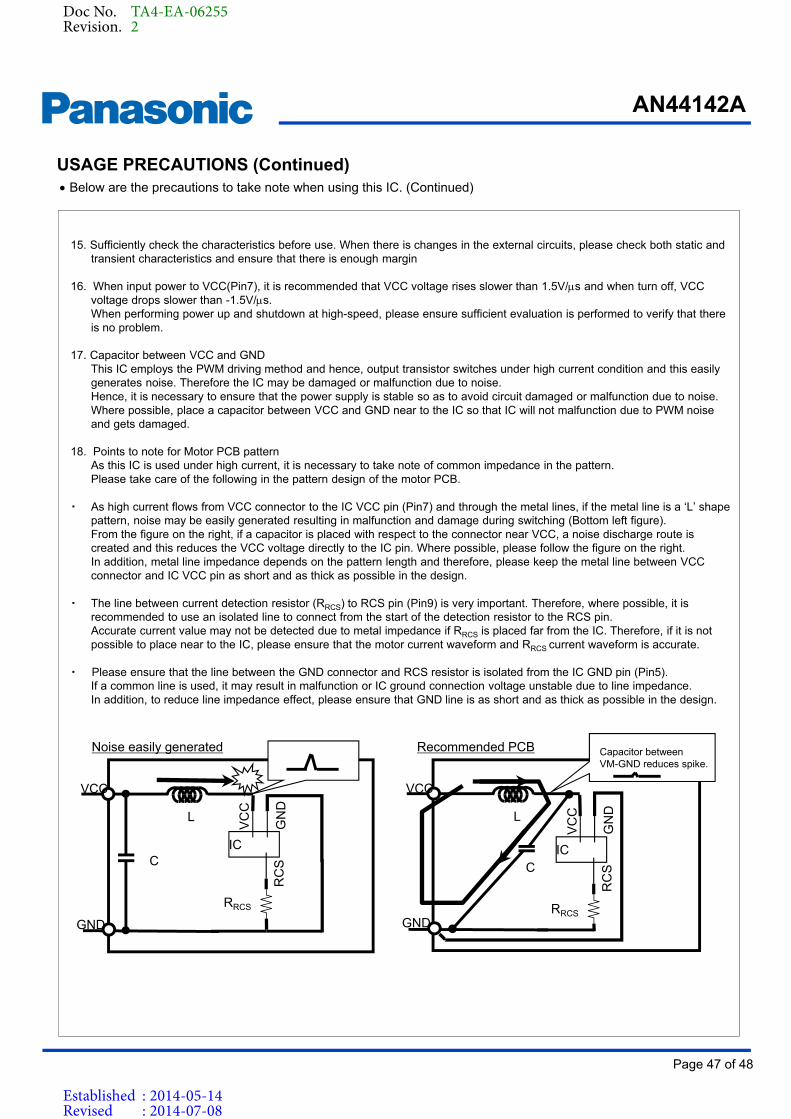
18. Points to note for Motor PCB patternAs this IC is used under high current, it is necessary to take note of common impedance in the pattern.Please take care of the following in the pattern design of the motor PCB.
・ As high current flows from VCC connector to the IC VCC pin (Pin7) and through the metal lines, if the metal line is a ‘L’ shape pattern, noise may be easily generated resulting in malfunction and damage during switching (Bottom left figure).From the figure on the right, if a capacitor is placed with respect to the connector near VCC, a noise discharge route is created and this reduces the VCC voltage directly to the IC pin. Where possible, please follow the figure on the right.In addition, metal line impedance depends on the pattern length and therefore, please keep the metal line between VCC connector and IC VCC pin as short and as thick as possible in the design.
・ The line between current detection resistor (RRCS) to RCS pin (Pin9) is very important. Therefore, where possible, it is recommended to use an isolated line to connect from the start of the detection resistor to the RCS pin.Accurate current value may not be detected due to metal impedance if RRCS is placed far from the IC. Therefore, if it is not possible to place near to the IC, please ensure that the motor current waveform and RRCS current waveform is accurate.
・ Please ensure that the line between the GND connector and RCS resistor is isolated from the IC GND pin (Pin5).If a common line is used, it may result in malfunction or IC ground connection voltage unstable due to line impedance.In addition, to reduce line impedance effect, please ensure that GND line is as short and as thick as possible in the design.
Noise easily generated
VCC
GND
L
C
Recommended PCB
VCC
GND
L
Capacitor between VM-GND reduces spike.
CIC
RC
S
VC
C
GN
D
IC
RC
S
VC
C
GN
D
USAGE PRECAUTIONS (Continued) Below are the precautions to take note when using this IC. (Continued)
RRCSRRCS
Doc No. TA4-EA-06255Revision. 2
Established : 2014-05-14Revised : 2014-07-08
Page 48 of 48
AN44142A
Product Standards
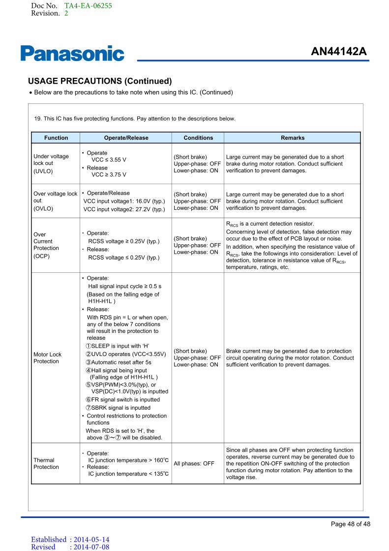
19. This IC has five protecting functions. Pay attention to the descriptions below.
Function Operate/Release Conditions Remarks
Under voltage lock out
(UVLO)
• OperateVCC ≤ 3.55 V
• ReleaseVCC ≥ 3.75 V
(Short brake)Upper-phase: OFFLower-phase: ON
Large current may be generated due to a short brake during motor rotation. Conduct sufficient verification to prevent damages.
Over voltage lock out
(OVLO)
• Operate/Release
VCC input voltage1: 16.0V (typ.)
VCC input voltage2: 27.2V (typ.)
(Short brake)Upper-phase: OFFLower-phase: ON
Large current may be generated due to a short brake during motor rotation. Conduct sufficient verification to prevent damages.
Over CurrentProtection
(OCP)
Operate:
RCSS voltage ≥ 0.25V (typ.)
Release:
RCSS voltage ≤ 0.25V (typ.)
(Short brake)Upper-phase: OFFLower-phase: ON
RRCS is a current detection resistor.
Concerning level of detection, false detection may occur due to the effect of PCB layout or noise.
In addition, when specifying the resistance value of RRCS, take the followings into consideration: Level of detection, tolerance in resistance value of RRCS, temperature, ratings, etc.
Motor LockProtection
• Operate:
Hall signal input cycle ≥ 0.5 s
(Based on the falling edge of H1H-H1L )
• Release:
With RDS pin = L or when open,any of the below 7 conditions will result in the protection to release
①SLEEP is input with ‘H’
②UVLO operates (VCC<3.55V)
③Automatic reset after 5s
④Hall signal being input(Falling edge of H1H-H1L )
⑤VSP(PWM)<3.0%(typ), or VSP(DC)<1.0V(typ) is inputted
⑥FR signal switch is inputted
⑦SBRK signal is inputted
• Control restrictions to protection functions
When RDS is set to ‘H’, the above ③~⑦ will be disabled.
(Short brake)Upper-phase: OFFLower-phase: ON
Brake current may be generated due to protection circuit operating during the motor rotation. Conduct sufficient verification to prevent damages.
ThermalProtection
Operate:IC junction temperature > 160
Release:IC junction temperature < 135
All phases: OFF
Since all phases are OFF when protecting functionoperates, reverse current may be generated due to the repetition ON-OFF switching of the protection function during motor rotation. Pay attention to the voltage rise.
USAGE PRECAUTIONS (Continued) Below are the precautions to take note when using this IC. (Continued)
Doc No. TA4-EA-06255Revision. 2
Established : 2014-05-14Revised : 2014-07-08
Request for your special attention and precautions in using the technical information and semiconductors described in this book
(1) If any of the products or technical information described in this book is to be exported or provided to non-residents, the
laws and regulations of the exporting country, especially, those with regard to security export control, must be observed. (2) The technical information described in this book is intended only to show the main characteristics and application circuit
examples of the products. No license is granted in and to any intellectual property right or other right owned by Panasonic Corporation or any other company. Therefore, no responsibility is assumed by our company as to the infringement upon any such right owned by any other company which may arise as a result of the use of technical information de-scribed in this book.
(3) The products described in this book are intended to be used for general applications (such as office equipment,
communications equipment, measuring instruments and household appliances), or for specific applications as expressly stated in this book.
Please consult with our sales staff in advance for information on the following applications, moreover please exchange documents separately on terms of use etc.: Special applications (such as for in-vehicle equipment, airplanes, aerospace, automotive equipment, traffic signaling equipment, combustion equipment, medical equipment and safety devices) in which exceptional quality and reliability are required, or if the failure or malfunction of the products may directly jeopardize life or harm the human body.
Unless exchanging documents on terms of use etc. in advance, it is to be understood that our company shall not be held responsible for any damage incurred as a result of or in connection with your using the products described in this book for any special application.
(4) The products and product specifications described in this book are subject to change without notice for modification and/or
improvement. At the final stage of your design, purchasing, or use of the products, therefore, ask for the most up-to-date Product Standards in advance to make sure that the latest specifications satisfy your requirements.
(5) When designing your equipment, comply with the range of absolute maximum rating and the guaranteed operating
conditions (operating power supply voltage and operating environment etc.). Especially, please be careful not to exceed the range of absolute maximum rating on the transient state, such as power-on, power-off and mode-switching. Other-wise, we will not be liable for any defect which may arise later in your equipment.
Even when the products are used within the guaranteed values, take into the consideration of incidence of break down and failure mode, possible to occur to semiconductor products. Measures on the systems such as redundant design, arresting the spread of fire or preventing glitch are recommended in order to prevent physical injury, fire, social damages, for example, by using the products.
(6) Comply with the instructions for use in order to prevent breakdown and characteristics change due to external factors (ESD,
EOS, thermal stress and mechanical stress) at the time of handling, mounting or at customer's process. We do not guarantee quality for disassembled products or the product re-mounted after removing from the mounting board.
When using products for which damp-proof packing is required, satisfy the conditions, such as shelf life and the elapsed time since first opening the packages.
(7) When reselling products described in this book to other companies without our permission and receiving any claim of
request from the resale destination, please understand that customers will bear the burden. (8) This book may be not reprinted or reproduced whether wholly or partially, without the prior written permission of our
company.
No.010618