an1697 application note - nxp...
TRANSCRIPT

(! # $)&"%! & $!(' $# ) ' %# $$% $#'&$! "
Prepared by: Jacques Trichet, Gilles Montoriol, Cyril Quennehen, Philippe Riondet, Brigitte Ray, Philippe DidierMotorola, Inc., Semiconductor Products Section, Wireless Subscriber Systems Group
INTRODUCTION
Dual band GSM900 and DCS1800 (or DCS1900) phonedesign puts a real challenge on Power Amplifier functionwhich needs to operate in two frequencies while providingappropriate isolation and control for each frequency.
This application note describes the dual band demoboardthat we have developed based on two single band PowerAmplifier ICs: MRFIC0919 and MRFIC1819, plus a dedicatedcontrol IC: MC33170 (product of ON Semiconductor).
DUAL–BAND DEMOBOARD
New IPA Generation
– Our previous range of 3.6 V GaAs IPAs (MRFIC0917 forGSM900 and MRFIC1817 for DCS1800/PCS1900) wasrequiring external negative voltage to operate which wasderived from a dedicated Power Management ICMC33169. The way to control the Power Amplifiers withthis IC is detailed in Application Note AN1599 and a dualband application using MRFIC0917, MRFIC1817 andMC33169 (product of ON Semiconductor) is described inApplication Note AN1602.
The MRFIC0919 and MRFIC1819 are the follow–up of theMRFIC0917 and MRFIC1817 w i th t h ree ma jo rimprovements:
– Absolutely Spur free Voltage Generators are included inthe IPA (based on synchronous rectification of the RFcarrier). A negative voltage is used for biasing the line–upand a positive step–up voltage for depleting the NMOSdrain switch FET.
– Better performances in terms of output power. This isparticularly of interest for dual band application where therecombination of the GSM900 and the
DCS1800/PCS1900 lines before the antenna inducesadditional insertion losses.
– Smaller packaging: both devices are housed in aTSSOP–16EP package which has an attractive size(5x6.5mm, maximum height of 1.2 mm) and an exposedbackside pad allowing excellent thermal and electricalperformances.
In addition, gain has been increased on MRFIC0919compared to MRFIC0917 allowing operation with input powerdown to 3.0 dBm. Both MRFIC0919 and MRFIC1819 arefeaturing three stages RF line–up.
Negative/Positive Voltage Generator
On both MRFIC0919 and MRFIC1819, RF rectification isused to build the dc bias voltage supply on chip (patentpending). The DC Voltage Generator (basically schottkydiodes and capacitor network) is connected at the output of adedicated buffer that samples and amplifies the RF inputsignal.
The key advantage of this built–in dc voltage generation isto remove the need of an external switching supply generatorwhich would require particular attention when laying out theboard due to possible spurious beside the RF carrier asmodulation sidebands.
– The negative voltage is high enough (–5.0 V) tosimultaneously bias the activated RF line up whiledisabling the other one through their gates.
– The positive voltage is used to drive an NMOS FETswitch that performs the Output Power Control accordingto the Drain Control method.
All those voltages are shared and used by the MC33170that in addition performs the band selection job by eithersetting correct biasing point to a path or turning it off.
Order this documentby AN1697/D
SEMICONDUCTOR APPLICATION NOTE
Motorola, Inc. 2000
REV 1
Fre
esc
ale
Se
mic
on
du
cto
r, I
Freescale Semiconductor, Inc.
For More Information On This Product, Go to: www.freescale.com
nc
...

2 MOTOROLA SEMICONDUCTOR APPLICATION INFORMATION
Figure 1. Block Diagram
MC33170*
; (" $A@ ("
; ( $A@ (
+0/@
(
+>/:=
)D;
+(( +%
+
+
+((
+%
+((
+%
07/? (
#"$((C7@16
MRFIC0919
MRFIC1819
+07/? ("(
07/? ("
>3E <D3? $
%><2A1@ <4 $# (3:71<;2A1@<>
Fre
esc
ale
Se
mic
on
du
cto
r, I
Freescale Semiconductor, Inc.
For More Information On This Product, Go to: www.freescale.com
nc
...
3MOTOROLA SEMICONDUCTOR APPLICATION INFORMATION
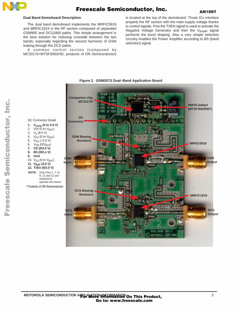
Dual Band Demoboard Description
The dual band demoboard implements the MRFIC0919and MRFIC1819 in the RF section composed of separatedGSM900 and DCS1800 paths. This simple arrangement isthe best solution for reducing crosstalk between the twobands; especially regarding the second harmonic of GSMleaking through the DCS paths.
A common con t ro l sec t ion ( composed byMC33170+MTSF3N02HD, products of ON Semiconductor)
is located at the top of the demoboard. Those ICs interfaceproperly the RF section with the main supply voltage thanksto control signals. First the TXEN signal is used to activate theNegative Voltage Generator and then the VRAMP signalperforms the burst shaping. Also a very simple selectioncircuitry enables the Power Amplifier according to BS (bandselection) signal.
Figure 2. GSM/DCS Dual–Band Application Board
NOTE: Only Pins 1, 7, 8, 9, 11 and 12 are required tooperate the board.
DC Connector Detail
1. Vramp (0 to 2.0 V)2. VDI (0 to VBAT)3. Vp (8.0 V)4. VD2 (0 to VBAT)5. VSS (–5.0 V)6. VDB (0/VBAT)7. CE (0/2.0 V)8. BS (0/2.o V)9. Gnd10. VD3 (0 to VBAT)11. VBAT (3.6 V)12. TxEn (0/2.0 V)
NMOS ballast(MTSF3N02HD*)
MRFIC0919
MRFIC1819
GSMOutput
DCSOutput
GSMInput
DCSInput
DCS BiasingResistors
Companion chipMC33170*
DCConnector
GSM BiasingResistors
%><2A1@? <4 $# (3:71<;2A1@<>
Fre
esc
ale
Se
mic
on
du
cto
r, I
Freescale Semiconductor, Inc.
For More Information On This Product, Go to: www.freescale.com
nc
...

4 MOTOROLA SEMICONDUCTOR APPLICATION INFORMATION
Application Schematic
The electrical schematic given hereafter is the referencecircuitry for the complete application. In particular it has been
used to populate the above PCB and on this demoboardhave been performed all the measurements that will follow.
Figure 3. Application Schematic
+0/@@
+>/:=
/;2 (3931@
)D;
=
;
' 8
' 8
' 8
;
;
=
;
=
=
' 8
' 8
' 8
=
=
=
! ;
! ;
! ;
! ;
! ;
!)
::
!)
::
!)
::!)
::
!)
::
=
;
=
=
=
;
=
=
!) !)
!)
!)
::
::
::
::
=
'
!)
:: !)
::
!)!)
::
::
=
=
' 8
' 8
' 8
;
;
=
=
=
=
=
( ;
(" ;
( $A@
(" $A@
<A0933320/18<; #"$()
,")(#
, "(
)D;
(
("
+
;2
+0/@@
#7;B
!$
;B
+=
$A@
+((
(
(
(
υ
+((
+(
+
;2
+
' ;
;2
+
7/?
7/?
7/?
' $A@
' $A@
' $A@
+
+=
,
%
+((
+(
+
+
' ;
;A4
+
+
7/?
7/?
7/?
' $A@
' $A@
' $A@
+
+=
,
%
!)!)!) .1 Ω!)!)!)!)!) .1 Ω!)!) !)!) .1 Ω!) .1 Ω(A0?@>/@3 ' > 756 & /=/17@<>?
%><2A1@? <4 $# (3:71<;2A1@<>
Fre
esc
ale
Se
mic
on
du
cto
r, I
Freescale Semiconductor, Inc.
For More Information On This Product, Go to: www.freescale.com
nc
...

5MOTOROLA SEMICONDUCTOR APPLICATION INFORMATION
Figure 4. Control Signals Timing for Burst Mode
' ;(
)D;
+>/:=
(" =<C3>@3:=9/@3
+
+
+
+
+
+
µ? µ? µ?
Burst Shaping
The association of both IPAs with the companion chipgives a unique solution suitable for fast burst operation thatcan wake–up from complete stand by mode (Current <10 µA)to full output power within the GSM power template. In orderto perform burst mode measurements, the following timingcan be used as a guide line.
Explanation:
– CE is activated at the very beginning of the burst(28 µs before the nominal part of the burst), this is alsothe right time to apply input power to the selected line up(Set Band Select appropriately).
– TxEn is activated 10 µs later to activate the buffer andgenerate Negative and Positive Voltage. The settling time
of negative and positive voltages is so short(<1.0 µs) that burst ramping can be initiated also.
– Vramp can start almost immediately after TxEn and issmoothly shaped in order to limit the switching transient(a simple linear ramp is good enough as shown on thenext plots).
– The falling down is performed the same way (but in thereverse order), and last even shorter (18us is enough).
Next plot shows the output power versus time for fourdifferent PCL (power control level) within the top 30 dB range.The exact same timing is kept for all PCL; only the nominalvoltage of Vramp is changed to set the nominal output power(within the useful part of the burst).
The four traces correspond to Vramp = 0.41, 0.52, 0.8 and1.9 V respectively. Also there is a gap in the time sweep (after50 µs) that removes the constant power section of the burst.
Fre
esc
ale
Se
mic
on
du
cto
r, I
Freescale Semiconductor, Inc.
For More Information On This Product, Go to: www.freescale.com
nc
...

6 MOTOROLA SEMICONDUCTOR APPLICATION INFORMATION
Figure 5. Power versus Time
A
*
TRG
1SA
2SA
3SA
4SA
EXT
PGL
PGH
1VIEW
2VIEW
3VIEW
4VIEW
Ref Lvl
40 dBm
RBW
VBW
SWT
ExtRef Marker 1 [T1]
36.00 dBm
40.000000 µs
1
1
100
MHz
MHz
µs
RF Att 20 dB
Unit dBm
10 µs/Center 900.015 MHz
37 dB Offset
Switching Spectrum
The second (but most severe) condition that anytransmitted GSM burst has to fulfill is the spectral mask or
output spectrum due to switching transient. A max holdmeasurement is used to check the possible spectraldegradation a few channels apart from the carrier.
Fre
esc
ale
Se
mic
on
du
cto
r, I
Freescale Semiconductor, Inc.
For More Information On This Product, Go to: www.freescale.com
nc
...

7MOTOROLA SEMICONDUCTOR APPLICATION INFORMATION
Figure 6. Output Spectrum (Max Hold)
A
1MA
EXT
STR
1VIEW
Ref Lvl
36 dBm
RBW
VBW
SWT
ExtRef Marker 1 [T1]
35.37 dBm
900.00200401 MHz
30
100
6
kHz
kHz
ms
RF Att 20 dB
Unit dBm
200 kHz/Center 900 MHz
37 dB Offset
Span 2 MHz
Open Loop versus Temperature
The Drain Control principle is stable and predictive enoughto be used in an open loop mode: this simply means that youdon’t need to sense the output power but simply trust the IPA
drain supply voltage. The following 2 measurements clearlyhighlight the good stability of the drain control versus eitherfrequency or temperature.
This control method will be thoroughly depicted in thesecond part of this application note.
Fre
esc
ale
Se
mic
on
du
cto
r, I
Freescale Semiconductor, Inc.
For More Information On This Product, Go to: www.freescale.com
nc
...

8 MOTOROLA SEMICONDUCTOR APPLICATION INFORMATION
Figure 7. Output Power versus Temperature
Pout (dBm) @ 898MHz
dB(Vramp–Voff )
°
°
°
Pout (dBm) @ 25°C
E D
dB(Vramp–Voff )
"F
"F
"F
!7;3/> "F
Figure 8. Output Power versus Frequency
Another tremendous advantage of the drain control technique is the very low ripple across the Tx band in all the usefuldynamic range (top 30 dB).
Fre
esc
ale
Se
mic
on
du
cto
r, I
Freescale Semiconductor, Inc.
For More Information On This Product, Go to: www.freescale.com
nc
...

9MOTOROLA SEMICONDUCTOR APPLICATION INFORMATION
CONTROL PHILOSOPHY
MRFIC0919 and MRFIC1819 application uses the draincontrol technique developed for our previous range of GaAsIPAs (refer to AN1599).
A NMOS FET is used to switch the IPA drain and vary thedrain supply voltage from 0 to battery voltage. As the NMOSFET requires higher voltage than Vbat to fully saturate it, apositive step–up voltage is generated inside the IPA for thatpurpose. An fast Operational Amplifier is included in theMC33170 and can be customized to provide proper transferfunction between control signal Vramp and IPA supply voltage.This OpAmp is connected using in a dual feedbackconfiguration: both the NMOS gate and source voltages areinjected back to the inverting input in order to maintain goodlinearity of control and avoid any saturation at the output ofthe OpAmp.
Indeed, the control has the benefit of providing lineartransfer function while also being repeatable versus controlvoltage and temperature variations. Therefore it appears as agood candidate for open loop configuration (the coupler andthe temperature compensation diode from the traditionalcontrol loop can be removed).
Double Feedback
In previous open loop application with MC33169 (seeAN1599), the control signal Vramp was multiplied by a fixed
gain amplifier and applied to the NMOS gate. Now thatMC33170 gives complete access to all pins of its internalOpAmp, one could imagine embedding the NMOS inside thefeedback loop to compensate for its threshold voltagevariation. This way a true linear law would be guaranteedbetween control voltage and IPA drain voltage hence RFvoltage. Although this concept is quite satisfactory for steadystate condition, it shows some penalty for the transientresponse. As a matter of fact, the OpAmp output can go highand saturate into its supply rail (when control voltage is toohigh or battery voltage too low) and exhibit a small delay torecover during the falling down of the burst. The immediateconsequence is to deteriorate the switching transientspectrum.
Double feedback is the good compromise to get the best ofboth solutions: it provides some compensation of Vth whileavoiding OpAmp saturation.
The following schematic will be used as the baseline todiscuss this concept and simulate its behavior. Note thatsome capacitors are included inside the circuitry to provide inaddition a Low–Pass filter characteristic. The IPA is simplymodeled by RPA and CPA.
Figure 9. Control Circuitry Schematic
+>/:=
+0/@
+
+>/:=
+
' 8 ' 8
=
' 8
' 8
' 8
,"
+3>>/:=
=
% ;
'%
+%
, ")(#
=
'
%><2A1@? <4 $# (3:71<;2A1@<>
Fre
esc
ale
Se
mic
on
du
cto
r, I
Freescale Semiconductor, Inc.
For More Information On This Product, Go to: www.freescale.com
nc
...

10 MOTOROLA SEMICONDUCTOR APPLICATION INFORMATION
Sweep on V ramp
The following plot represents the gate voltage and sourcevoltage of the NMOS versus Vramp.
Vramp is swept from 0 to 2.0 V. Curve #1 is the IPA supplyvoltage and curve #2 is the output voltage of the OpAmp. Thelater shows 3 different portions:
– The first one (slope = divider ratio between R5 andR3//R4, i.e. G1=(R5+R3//R4)/(R3//R4)) occurs when theNMOS is off (no feedback via the VPA voltage). Thishigher slope contributes to reduce the dead zone beforereaching VGSth (approximately 1.1 V for this NMOS fet).
– The smaller one (divider ratio between R5//R4 and R3)occurs when the NMOS is in its ohmic region as a voltagefollower. This is the useful portion covered for linear Poutcontrol.
– The third one (slope = divider ratio between R5 andR3//R4) occurs when the NMOS is saturated (no morefeedback via the VPA voltage that is limited by Vbat). Thishigher slope is useful to still increase the NMOS gatevoltage while avoiding OpAmp saturation.
Figure 10. DC Transfer Function
"
" "
+% B3>?A? +>/:= +
A>B3
A>B3
+
''
"
%7;
+$
!)(
+%
7;+
$!)
(
Fre
esc
ale
Se
mic
on
du
cto
r, I
Freescale Semiconductor, Inc.
For More Information On This Product, Go to: www.freescale.com
nc
...

11MOTOROLA SEMICONDUCTOR APPLICATION INFORMATION
Bessel Type LPF
The most appropriate transfer function to realize the burstshaping is a Bessel type since its pulse response exhibitsmooth transition with no overshoot. The switching transientsare also minimized after the shaping.
A 2 pole Bessel filter is embedded in the OpAmp externalcircuitry as a Salen–Key topology. The gain used to computecomponent value is the smaller one of second portion (dividerratio between R5//R4 and R3: G2 = (R3 + R4//R5)/R3 = 2.7).
Note that R3, R4 and R5 are used to set the gain valuethen only R1, R2, C1 and C2 determine the filter
characteristic. The theoretical values of those componentsfor a cut–off frequency of 60 kHz are:
R1 = 3.0 k, R2 = 13 k, C1 = 330 pF, C2 = 330 pF.
Closest normalized value were chosen instead and usedfor the simulation without significant difference.
Transfer Function (Bode Plot)
Cut–off frequency is around 63 kHz, with dc gain about8.0 dB.
Figure 11. Simulated Frequency Response
8 8 8 8 8
+ +% B3>?A? '&*#- F
A>B3
A>B3
%
(
+%
'
(
+
+%
+
8 8 8
Fre
esc
ale
Se
mic
on
du
cto
r, I
Freescale Semiconductor, Inc.
For More Information On This Product, Go to: www.freescale.com
nc
...

12 MOTOROLA SEMICONDUCTOR APPLICATION INFORMATION
Pulse Response
At last the time domain response to a rectangular pulse isshows hereafter. The settling time is about 7us withoutovershoot as expected.
It is clear that in real application the control voltage Vrampcan be much more sophisticated because it is generated by a
dedicated DAC using look–up tables for ramp up and down.Indeed, this signal looks like a staircase that can approximateoptimum rising/falling edges with minimal spectral content.Anyway, the same low pass filter characteristic is still requiredto smooth this staircase.
Figure 12. Simulated Time Transient
* * * * *
"
+% B3>?A? ) " ?31
A>B3
A>B3
+'
"
%
+
+%
+
Fre
esc
ale
Se
mic
on
du
cto
r, I
Freescale Semiconductor, Inc.
For More Information On This Product, Go to: www.freescale.com
nc
...

13MOTOROLA SEMICONDUCTOR APPLICATION INFORMATION
CONCLUSION
The dual band Power Amplifiers demo board described inthis application note is a stand alone system solution for dualband transmitters. Using off–the–shelf mono band IPAs plusa dedicated controller, one can easily meet the GSM ETSIrecommendations with a rugged, simple but innovativearchitecture.
The “open loop” concept for controlling Pout isdemonstrated as a viable solution with key advantages:
– Suppression of the coupler leads to minimize theinsertion losses after the PA.
– Suppression of the detector diodes and their possiblecompensation circuitry.
– At last but not least, it eases the calibration of thetransmitter (thanks to its superior predictability, linearityand reproducibility) and shortens the production time forthat phase.
REFERENCES
1. MRFIC0919 Data Sheet: 3.6 V GSM 900 MHz GaAsIntegrated Power Amplifier.
2. MRFIC1819 Data Sheet: 3.6 V DCS 1800 MHz GaAsIntegrated Power Amplifier.
3. MC33170 Data Sheet: High Performance IntegratedDriver for Dual–Band RF Power Amplifiers. (Product ofON Semiconductor)
4. AN1599 Application Note: Power Control with theMRFIC0913 GaAs Integrated Power Amplifier andMC33169 Support IC.
5. AN1602 Application Note: 3.6 V and 4.8 VGSM/DCS1800 Dual Band PA Application with DECTCapability Using Standard Motorola RFIC’s.
Fre
esc
ale
Se
mic
on
du
cto
r, I
Freescale Semiconductor, Inc.
For More Information On This Product, Go to: www.freescale.com
nc
...

14 MOTOROLA SEMICONDUCTOR APPLICATION INFORMATION
NOTES
Fre
esc
ale
Se
mic
on
du
cto
r, I
Freescale Semiconductor, Inc.
For More Information On This Product, Go to: www.freescale.com
nc
...

15MOTOROLA SEMICONDUCTOR APPLICATION INFORMATION
NOTES
Fre
esc
ale
Se
mic
on
du
cto
r, I
Freescale Semiconductor, Inc.
For More Information On This Product, Go to: www.freescale.com
nc
...
16 MOTOROLA SEMICONDUCTOR APPLICATION INFORMATION
Motorola reserves the right to make changes without further notice to any products herein. Motorola makes no warranty, representation or guarantee regardingthe suitability of its products for any particular purpose, nor does Motorola assume any liability arising out of the application or use of any product or circuit, andspecifically disclaims any and all liability, including without limitation consequential or incidental damages. “Typical” parameters which may be provided in Motoroladata sheets and/or specifications can and do vary in different applications and actual performance may vary over time. All operating parameters, including “Typicals”must be validated for each customer application by customer’s technical experts. Motorola does not convey any license under its patent rights nor the rights ofothers. Motorola products are not designed, intended, or authorized for use as components in systems intended for surgical implant into the body, or otherapplications intended to support or sustain life, or for any other application in which the failure of the Motorola product could create a situation where personal injuryor death may occur. Should Buyer purchase or use Motorola products for any such unintended or unauthorized application, Buyer shall indemnify and hold Motorolaand its officers, employees, subsidiaries, affiliates, and distributors harmless against all claims, costs, damages, and expenses, and reasonable attorney feesarising out of, directly or indirectly, any claim of personal injury or death associated with such unintended or unauthorized use, even if such claim alleges that Motorolawas negligent regarding the design or manufacture of the part. Motorola and are registered trademarks of Motorola, Inc. Motorola, Inc. is an EqualOpportunity/Affirmative Action Employer.
How to reach us:USA/EUROPE/Locations Not Listed : Motorola Literature Distribution; JAPAN : Motorola Japan Ltd.; SPS, Technical Information Center, P.O. Box 5405, Denver, Colorado 80217. 1–303–675–2140 or 1–800–441–2447 3–20–1, Minami–Azabu, Minato–ku, Tokyo, 106–8573 Japan.
81–3–3440–3569
Customer Focus Center: 1–800–521–6274 ASIA/PACIFIC : Motorola Semiconductors H.K. Ltd.; Silicon Harbour Centre,2, Dai King Street, Tai Po Industrial Estate, Tai Po, N.T., Hong Kong.
HOME PAGE: http://www.motorola.com/semiconductors 852–26668334
AN1697/D◊
Fre
esc
ale
Se
mic
on
du
cto
r, I
Freescale Semiconductor, Inc.
For More Information On This Product, Go to: www.freescale.com
nc
...