an electrostatic microvalve for pneumatic control of
TRANSCRIPT

AN ELECTROSTATIC MICROVALVE FOR PNEUMATIC
CONTROL OF MICROFLUIDIC SYSTEMS
by
Douglas Anjewierden
A thesis submitted to the faculty of
The University of Utah
in partial fulfillment of the requirements for the degree of
Master of Science
Department of Mechanical Engineering
The University of Utah
May 2011
Copyright © Douglas Anjewierden 2011
All Rights Reserved

T h e U n i v e r s i t y o f U t a h G r a d u a t e S c h o o l
STATEMENT OF THESIS APPROVAL
The thesis of Douglas Anjewierden
has been approved by the following supervisory committee members:
Bruce K. Gale , Chair 3/14/2011
Date Approved
Kuan Chen , Member 3/14/2011
Date Approved
Meredith Metzger , Member 3/14/2011
Date Approved
and by Timothy Ameel , Chair of
the Department of Mechanical Engineering
and by Charles A. Wight, Dean of The Graduate School.

ABSTRACT
An electrostatic microvalve for the pneumatic control of microfluidic devices is
designed, modeled, fabricated, and characterized. The valve consists of several,
individually manufactured pieces assembled to form a microvalve. This creates an
inexpensive microvalve that can be easily and quickly manufactured. The unique feature
of this microvalve is its ability to be integrated with a microfluidic system for good
portability. The valve was manufactured by depositing a thin chrome layer on a
Poly(methyl methacrylate) substrate. Thin copper foil was used as a flexible membrane
that would deflect to allow air flow. When a voltage was applied between the chrome
layer and the copper foil, the electrostatic force pulled the foil closed against the substrate
and stopped the air flow. Parylene C was selected as a dielectric layer to provide
insulation and prevent short circuiting between the chrome and copper electrodes. The
valve was designed using a flexible, proximal electrode concept that decreased the
required closing voltage. A mathematical model was developed to predict the voltage
required to close the valve. Tests were performed to determine the closing voltage and
flowrate through the valve. The parylene dielectric thickness and the valve cavity depth
were varied to find the best valve parameters. It was determined that a valve with a 6 µm
layer of parylene with a 58 µm cavity depth provided the best combination of low closing
voltage and high flowrate. These valves were tested to work at pressures up to 40 kPa
with an average closing voltage of 680 V and an average flowrate of 1.05 mL/min. The

iv
valve showed that it also may be able to function as a flowrate control valve at higher
pressures, i.e., greater than 40 kPa. It was found that dielectric charging was occurring in
the valve during operation. Switching the polarity of the control voltage with each
actuation was a proposed solution that was tested and found to delay the onset of
dielectric charging. Finally, the valve was successfully used to pneumatically control
flow in a simplified microfluidic device.

TABLE OF CONTENTS
ABSTRACT....................................................................................................................... iii
LIST OF FIGURES .......................................................................................................... vii
ACKNOWLEDGEMENTS............................................................................................... ix
Chapter
1 INTRODUCTION...........................................................................................................1
Background .....................................................................................................................1
Motivation .......................................................................................................................2
Microvalves .....................................................................................................................4
Electrostatic Actuators ....................................................................................................5
2 VALVE DESIGN..........................................................................................................11
Overview .......................................................................................................................11
Design............................................................................................................................12
Initial Prototype.............................................................................................................16
Conclusion.....................................................................................................................19
3 MATERIALS AND FABRICATION...........................................................................20
Overview .......................................................................................................................20
Electrode – Valve Plate .................................................................................................21
Conductive Membranes.................................................................................................23
Dielectric Layer .............................................................................................................25
Cavity Plate ...................................................................................................................26
Interface and Assembly .................................................................................................26
Conclusion.....................................................................................................................27
4 TESTING AND RESULTS ..........................................................................................29
Overview .......................................................................................................................29
Test Methods .................................................................................................................30
Results ...........................................................................................................................32

vi
Dielectric Charging .......................................................................................................38
Integration with Microfluidics.......................................................................................40
Conclusion.....................................................................................................................41
5 CONCLUSION .............................................................................................................43
Summary .......................................................................................................................43
Future Work ..................................................................................................................45

LIST OF FIGURES
Figure Page
1. PDMS lab-on-a-chip used for DNA extraction .............................................................. 2
2. Diagram of the microfluidic valve system...................................................................... 3
3. Solenoid valves for off-board pneumatic control of a PDMS lab-on-a-chip.................. 3
4. Different electrostatic actuators using curved electrodes ............................................. 10
5. Electrostatic valve design using a membrane that deflects into a channel ................... 13
6. Valve operation............................................................................................................. 13
7. Theoretical closing voltage and break down voltage.................................................... 17
8. A picture of the prototype device.................................................................................. 17
9. PMMA valve plate with a Kapton tape shadow mask.................................................. 22
10. Patterned chrome over the valve holes with a trace leading to a bond pad ................ 22
11. Diagram of interface device........................................................................................ 28
12. Final assembled device with two valves ..................................................................... 28
13. Interaction plots between variables............................................................................. 34
14. Results for valves tested with 6 µm parylene layer and 58 µm cavity depth ............. 36
15. Flowrate as a function of voltage................................................................................ 37
16. Evidence of closing voltage drift caused by dielectric charging ................................ 38
17. Valves tested for dielectric charging........................................................................... 39
18. Diagram of the electrostatic valve connected to the microfluidic membrane valve... 41

viii
19. Array of 64 valves on a single PMMA chip ............................................................... 46

ACKNOWLEDGEMENTS
I would like to first thank Dr. Bruce Gale, my advisor, for his guidance,
instruction, and support on this project. Thank you to Greg Liddiard for his contribution,
help, and advice with the concept and design, and especially the many hours he spent in
the microfabrication lab. I appreciate the help of other students as well. I would also like
to show gratitude to my parents, who have supported and encouraged my education
throughout my life. Most of all, thank you to my wife, Molly, for her love, patience,
support, and understanding through the many hours I have worked on this project and the
years I have spent in school.

CHAPTER 1
INTRODUCTION
Background
Microfluidics is a growing field for research and development partly due to its
biological applications, such as drug delivery and pathogen detection. Specifically, a
wide variety of work has been done on integrated biochip devices for DNA analysis [1].
These biochip devices consist of microfluidic mixers, microvalves, micropumps, and
microchannels. The full integration of these systems allows for quick fluid transfer and
increased portability. However, there is still much work to be done on microfluidic
control systems. While the microfluidic systems themselves have a small footprint, often
the necessary support equipment is bulky and nonportable. For example, many
microfluidic systems rely on external valves to provide valving internal to the
microfluidic chip. As the number of internal valves can run into the hundreds or even
thousands, the number of external valves and the size and cost associated with them is a
significant problem. Thus, the development of the actuation and control elements for the
internal microfluidic components has not kept up with the miniaturization of
microfluidics [2].

2
Motivation
Work is currently being done at the University of Utah to develop a system to
extract DNA from a sample of blood. This system uses a lab-on-a-chip device, shown in
Figure 1. A lab-on-a-chip is a device that integrates several lab functions onto a single
chip to allow for a small footprint and a portable system. This particular lab-on-a-chip is
made of polydimethylsiloxane (PDMS). It uses microfluidic channels, micropumps, and
microvalves to mix the necessary chemicals and reagents to extract DNA.
This lab-on-a-chip device uses pneumatic internal valves that are controlled by
external valves. An example of this valve system is shown in Figure 2. In this design, the
pressure from the fluid deflects a membrane to allow fluid flow. When a pressure is
applied to the other side of the membrane, the membrane is closed against a valve seat.
Figure 1: PDMS lab-on-a-chip used for DNA extraction.

3
(a) (b)
Figure 2: Diagram of the microfluidic valve system. a) Pressure from the
fluid deflects the membrane to allow fluid flow. b) Pressure from the off-
board pneumatics closes the membrane valve and stops fluid flow.
Currently the external valves used to control the pneumatics are solenoid valves.
These solenoid valves are expensive, bulky, and they are not integrated very well with the
device. Figure 3 shows the tubing required to interface the external solenoid valves with
the PDMS lab-on-a-chip. There is a need to design a microvalve for the control of the
pneumatics of this system that is small, portable and easily integrated with the rest of the
system.
Figure 3: Solenoid valves for off-board pneumatic control of a PDMS lab-on-a-chip.

4
Microvalves
One of the most important control elements in a microfluidic system is
microvalves, which are used to control the timing, location, and rate of flow in a
microfluidic system. There are many different types of microvalves: magnetic,
electrokinetic, piezoelectric, thermo pneumatic, electrochemical, phase change,
rotary, and electrostatic, as well as different passive microvalves [3, 4].
There are several characteristics desirable when designing microvalves,
such as low leakage rate, short response time, wide operational temperature range,
low power consumption, and a small footprint. A wide variety of valves have
been published that can play this role in silicon devices, but with the movement to
elastomeric plastics, there is a limited set of valves that function well. Many of
these valves rely on pneumatics that are controlled by external valves. Full
integration into a microfluidic system is an attractive characteristic of a valve, but
may not always be practical or desired, especially if the microfluidic chip is to be
disposable. Thus, the internal/external valve dichotomy is not necessarily a
concern if it can be handled in a manageable way.
The purpose of the research presented here was to design a microvalve
that is inexpensive, easy to manufacture, has a small footprint, can function as an
external valve controlling a pneumatic internal valve, and can be easily integrated
with a complex polymer microfluidic system. Electrostatic valves were chosen for
this work because these valves have low power consumption, a fast response time,
are electrically based, and are independent of ambient temperature [5, 6].

5
Electrostatic Actuators
The valve used in this work is based on electrostatic actuation. Electrostatic
actuation uses two electrodes that are separated by a gap. When a voltage is applied
across the electrodes, an electric field is generated which creates an electrostatic force
between the electrodes. This force can be used to move one or both of the electrodes. The
equation for electrostatic force of a system is given by
2
2
2g
AVF ao
e
εε= , (1)
where εo is the vacuum permittivity, εa is the dielectric constant of the air between
electrodes, A is the area of the electrode, V is the voltage across the electrodes and g is the
total distance between electrodes [7].
Electrostatic actuation has been used to pump fluids in a microfluidic system. In
one publication, electrostatic actuation of a parylene membrane was used to pump fluid
based on a three-phase peristaltic sequence [6]. This design was surface micromachined
using what is described as a multilayer parylene technology. Another publication had a
pump design that used a micro membrane based on bulk micromachining of silicon
wafers [8]. This pump used electrostatic force to deflect a membrane outward and force a
fluid flow through the inlet valve into the pump chamber. When the electrostatic
actuation was turned off the membrane bent back and forced the fluid through the outlet
valve.
Unlike these micropumps, most electrostatic microvalves are used to control gas
flow, which is the purpose here, rather than liquid flow due to electrolysis of liquids at

6
the high operational voltages [3]. In the case of microvalves, there have been reports of
using a flexible membrane [9] or a silicon valve plate [5]. The flexible membrane [9]
used a conductive membrane actuated between an upper and lower chamber. The
conductive membrane was a three-layer membrane consisting of a gold layer between
two insulating polyimide layers, each layer being 1 µm thick. This microvalve was
reported to operate at a differential pressure of up to 110 kPa at a flowrate of 12 mL/min
with an applied voltage of approximately 60-150 V. Another microvalve [5] used a
silicon valve plate as part of a three-layer silicon chip stack to operate as a normally-
closed electrostatically-driven three-way microvalve. This valve was reported to operate
at pressures up to 10 bar (1 MPa) with a flowrate of approximately 500 mL/min using an
actuation voltage of 200 V. These results are summarized in Table 1.
These valves are manufactured using fabrication techniques that can be time
consuming and expensive. The flexible membrane valve [9] uses thermal injection
molding which required molds to be milled. The membrane electrode fabrication required
micromachining and photolithography. The silicon valve [5] required bulk
micromachining of three separate silicon layers. This required wet and dry etching
techniques as well as a silicon fusion bond process to bond the three silicon layers. A
simpler, faster, less expensive manufacturing process was desired for the valve designed
in this paper.
There have also been reports [10] of electrostatic valves using an air pressure
balance to allow the valve to operate at high pressures. This design had pressure
compensation using an air chamber to support a membrane. As the air pressure balanced
the fluid pressure, the electrostatic actuator opened the valve. This design has been

7
Table 1: Results of different electrostatic microvalves found in literature.
Valve Description Control
Voltage (V)
Pressure
(kPa)
Flowrate
(mL/min)
Flexible Membrane [9] 60-150 110 12
Silicon Valve Plate [5] 200 1000 500
Simulation of Pressure
Balance [10] -- 1200 0.0086
reported to function at fluid pressures up to 10 atm (1.013 MPa). This valve requires
another pneumatic line for the pressure balance and adds complexity to the design. This
would not be effective for the work presented here, as the purpose of the valve was to be
a simple design without the requirement of excess operational equipment. The simulation
results done as part of this work are summarized in Table 1.
Upon review of literature, the manufacturing methods used to produce the
existing valve designs are a major limiting factor. The focus of the work presented here is
to design a microvalve with more practical manufacturing methods. A microvalve that
can be quickly and inexpensively manufactured in bulk quantities would be very
beneficial from a commercialization and implementation standpoint.
Another disadvantage of electrostatic actuators is the difficulty of achieving large
displacements. From equation 1, electrostatic force increases exponentially as the
distance between electrodes decreases. Thus it is important to consider the distance
between electrodes when designing valves. Since the electrodes need to be as close
together as possible to generate the highest force, this creates a design challenge when a
large displacement and a large flow between the plates are desired. Some solutions have

8
been proposed [11-13], though they have been reported only as a single valve and not as
an integrated valve array with any practical application.
This project has incorporated the idea of a curved film electrode. The purpose of
the curved electrode is to keep the electrodes close together on one end of the actuator
while allowing the other end of the actuator to make large displacements. When a voltage
is applied, the force is strong at the end where the electrodes are close together and brings
the electrode together at that end. The electrostatic force then increases further towards
the other end of the valve and continues to move the electrodes closer together, which
causes the electrodes to roll together.
This idea can be accomplished in two ways. One proposed way is an electrostatic
actuator that has a stationary curved electrode [11], as shown in Figure 4a. In this design,
the straight, flexible membrane can curl against the stationary electrode. Numerical
calculations have been published [14] to find the bending performance of electrostatic
actuators with different shapes of the electrode and the actuator.
The other design to achieve large displacements with a curved electrode uses a
flexible membrane as a curved electrode, shown here in two different cases. In one
published case the membrane is curled up by residual stress during manufacturing [12],
shown in Figure 4b. This is accomplished because of the stress that occurs during the
deposition of the silicon dioxide and chrome to form the membrane. Because the upper
layer of chrome is in tension and the lower layer of silicon dioxide is in compression, the
membrane will curl up when the sacrificial layer is removed. This valve design was
reported to use a closing voltage of 30 V in the absence of gas flow. The second
published case uses a conductive film between sandwiched between two electrodes [13],

9
shown in Figure 4c. The film has an S-shaped bend in the middle that rolls back and forth
as a voltage is alternately applied between each of the electrodes and the film. A
propagation speed of 4.0 m/s is reported when an applied voltage is 150 V. This concept
can be used as a microvalve with the membrane rolling over the inlet and outlet holes.
This paper presents an electrostatic microvalve for pneumatic control of
microfluidic channels that is low cost, quickly and easily manufactured, has a small
footprint, and could be manufactured in a large scale array. The uniqueness of the valve
presented in this thesis is its ability to be integrated with a complex polymer microfluidic
system.
This electrostatic valve aims to eliminate the need for the off-board solenoid
valves. The electrostatic valve presented in this paper will be able to be manufactured as
an array of many valves on a single chip no larger than a microscope slide. This valve
array will then be layered below the microfluidic layer to create a portable, low cost
system. This thesis describes the design, operation, fabrication, and performance of a
single electrostatic valve.

10
(a) (b)
(c)
Figure 4: Different electrostatic actuators using curved electrodes. (a) The
curved electrode is stationary and the membrane curls around it [11]. (b)
The membrane is curled up by residual stress that is induced during
manufacturing [12]. (c) An S-shaped film rolls back and forth between
two electrodes [13].

CHAPTER 2
VALVE DESIGN
Overview
The electrostatic microvalve uses the principle of electrostatic attractive force.
When a voltage is applied across two electrodes, the electric field generates a force
between them. This valve uses that attractive force to pull a membrane closed over the
valve inlet and outlet holes to stop air flow. The electrostatic force is inversely
proportional to the square of the gap between the electrodes, so it is important to keep the
electrodes as close together as possible. This need for having the electrodes close together
is addressed by the idea of a curved electrode to keep the electrodes close together at one
end, and the electrodes can have larger separation at the other end. A balance of the
forces acting on the valve membrane was used to develop an equation that would predict
the voltage required to close the valve.
A prototype was successfully tested that used a smooth aluminum plate as the
stationary electrode and a piece of 10 µm copper foil as the membrane. PDMS was spun
on the copper foil as a dielectric layer to prevent the electrodes from shorting out. A piece
of Poly(methyl methacrylate) (PMMA) was etched to create a channel for the valve.
These pieces were assembled and held together using C-clamps. The prototype was
successful at pressures up to 3 kPa. This was a proof of concept that the idea of

12
sandwiching individually manufactured pieces to form an electrostatic microvalve could
work. From this prototype, several changes to materials and fabrication were made that
would make the valve more reliable and useful at higher pressure.
Design
The research presented in the previous chapter of this thesis contributed to the
design of this electrostatic valve. The design is based on the idea that several pieces will
be “sandwiched” together to form the valve. A flexible conductive membrane is used,
along with an electrode above a cavity, to open and close the air flow. A dielectric layer
was deposited on both electrodes to prevent shorting out the valve. A concept drawing
showing the layers of the valve is shown in Figure 5.
The operation of the valve is shown in Figure 6. In Figure 6a, the air flows
through a microchannel, deflects the conductive membrane into a cavity, and air flow
continues through the microchannel. Since the membrane is close to the top electrode at
the edges of the cavity, the electrostatic force is high in these areas when a voltage is
applied. The membrane can move closed against the other electrode around the edges and
then the electrostatic force increases further toward the middle of the valve, as in Figure
6b. In this way the membrane can roll closed when a voltage is applied, as in Figure 6c. It
is important that the electrodes do not come into contact with each other, to prevent a
short circuit. For this reason an insulating layer was placed between the electrodes. It is
desirable for this insulating layer to be as thin as possible without allowing breakdown.

13
Figure 5: Electrostatic valve design using a membrane that deflects into a
channel. This uses the curved electrode principle, keeping the electrodes
close together around the edges.
(a) (b)
(c)
Figure 6: Valve operation. (a) Voltage off, valve fully open (b) Voltage
on, valve starting to close (c) Voltage on, Valve fully closed.
14
A theoretical model was made to predict the closing voltage when the valve is
completely open, as in Figure 6a. A force balance was performed on the membrane and
can be represented by,
0=++ ase FFF , (2)
There are three forces acting on the valve membrane: the electrostatic force, Fe, pulling
up on the membrane, the spring force, Fs, pulling up on the membrane, and the force
from the air pressure, Fa, pushing down on the membrane.
The force from the air was found by multiplying the air pressure by the area of the
cavity. The spring force in the membrane was found by multiplying the spring constant of
the membrane by the deflection of the membrane. The spring constant of a fixed-fixed
beam with uniform loading was used for the membrane. This is a conservative
assumption since the membrane is attached at the opposite ends and is not actually a
beam. The membrane is an electrode-dielectric composite; however, the spring constant
that was used only accounted for the spring constant of the electrode alone, as the
dielectric has a low modulus of elasticity.
The electrostatic force was broken up into two parts. The first part was the
electrostatic force acting across the cavity. The equation for electrostatic force can be
modified to find the electrostatic force through two dielectrics [15]. This is done by
changing the electrode gap g in equation 1 to use an effective gap T, given by

15
)1(b
a
dtgTε
ε−−= , (3)
where g is the separation between electrodes, td is the thickness of the insulating layer, εa
is the dielectric constant of the air, and εb is the dielectric constant of the insulator. The
second electrostatic force was the force that was acting around the edges of the cavity.
This electrostatic force was only acting through the insulating layer. The area this force
acted across was the area of the top electrode that overlapped around the edges of the
cavity.
The two electrostatic forces, the air force, and the spring force were inserted into
equation 2, which gives
022
12
2
2
2
2
1 =−++ PAkgT
VA
t
VA ao
d
ao εεεε, (4)
where A1 is the area of the cavity, and A2 is the overlap area of the electrode around the
edge of the cavity, k is the spring constant of the membrane, and P is the pressure of the
air. Equation 4 was then solved for the voltage and is given by
+
−=
2
2
2
1
0
1 )(2
T
A
t
A
kgPAV
d
aεε
, (5)

16
Equation 5 gave the voltage required to balance the forces on the membrane. Any
increase above this voltage would cause the membrane to start to close. Once the
membrane starts to move, the area the air acts on decreases and the electrostatic force
increases. The membrane will therefore be able to completely close.
Equation 5 was used to calculate the closing voltage for a valve that used a
parylene C dielectric layer and valve parameters shown in Figure 5. The parylene
thickness was varied and the resulting closing voltage is shown in Figure 7, along with
the breakdown voltage based on a dielectric strength of 267 V/ µm for parylene C. The
dielectric strength is the maximum electric field a material can withstand before breaking
down.
Initial Prototype
One main goal in designing this microvalve is to minimize the need for
fabrication that may be expensive or time consuming. For this reason the valve was
constructed using a sandwich concept, which would minimize the need for
microfabrication techniques. An initial prototype was made to test the sandwich concept.
This prototype used a polished plate of aluminum as the top electrode and a 10
µm-thick copper foil as the conductive membrane. A thin layer of PDMS was spun on to
the copper foil as a dielectric. The cavity was made by etching into PMMA using a CO2
laser (VersaLASER VLS 3.60, AZ, USA). An air line was interfaced with the aluminum
plate using another piece of PMMA. The device was held together using C-clamps. A
picture of the prototype is shown in Figure 8.
17
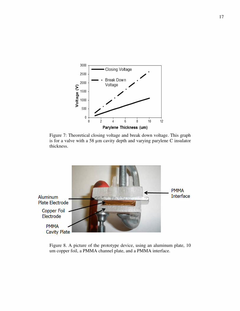
Figure 7: Theoretical closing voltage and break down voltage. This graph
is for a valve with a 58 µm cavity depth and varying parylene C insulator
thickness.
Figure 8. A picture of the prototype device, using an aluminum plate, 10
um copper foil, a PMMA channel plate, and a PMMA interface.

18
Testing for this prototype was done by placing the outlet tube in a beaker of
water. This was done so bubbles could be observed if flow was present. A voltage source
(EMCO, CA05P, CA, USA) of 500 V was used. The power consumption is negligible
because when the valve is held in the closed state for a long period, there is no current
flowing through the system. The valve proved to work at low pressures, around 3 kPa.
This prototype was a demonstration that the sandwich concept could work for
fast, inexpensive fabrication. Several failure modes were discovered that assisted work
moving towards a smaller valve that could work at higher pressures. The most common
failure mode was dielectric breakdown between the two electrodes (the aluminum and
copper layers). The large current flow associated with a high voltage short damaged the
metal and PDMS layers. It is believed this failure was due to contamination on the PDMS
layer, as well as pinholes in the PDMS that are caused when spinning a thin layer.
It was determined these problems would be remedied in several ways. First, the
assembly of the valve would need to take place in a cleaner environment to avoid
contamination that would damage the insulating layer. Second, a smoother electrode than
the aluminum plate would be used. It was believed the insulator could be damaged due to
a rough electrode surface. Additionally, a dielectric would be used with a higher
dielectric strength and less pinholes than PDMS. Finally, an insulating layer would be
placed on the stationary electrode, as well as the membrane, to minimize the effects of
damage and inconsistencies on the insulating layer.

19
Conclusion
This valve uses the principle of an electrostatic force between two electrodes. One
of these electrodes is a conductive, flexible membrane, while the other is a conductive
plate with inlet and outlet holes. This design uses the idea of a curved electrode. The
membrane will stay close to the top electrode at the edges of the cavity and the middle of
the electrode is free to deflect into a channel. When a voltage is applied, this will allow
for a high force where the electrodes are close together and the membrane can move
closer around the edges of the valve. The force then increases towards the middle of the
valve and the membrane can move further closed. In this manner the membrane can roll
closed. A theoretical model was developed to predict the closing voltage of the valve.
This valve uses a sandwich concept to allow for fast, inexpensive fabrication.
Pieces can be mass manufactured separately and then assembled to form the valve. A
prototype was developed to test this concept. An aluminum plate was used along with a
copper membrane and a PMMA base with a channel. PDMS was used as a dielectric
layer to prevent the valve from shorting out. Several lessons were learned from
developing and testing the prototype that would prove useful in designing a final valve
design. The materials and fabrication methods used in the final design are described in
detail in the following chapter of this thesis.

CHAPTER 3
MATERIALS AND FABRICATION
Overview
As previously described, the electrostatic valve is made by sandwiching together
several pieces. Those pieces include a valve plate, a conductive membrane, and a cavity
plate. A variety of standard microfluidic materials and methods were used to fabricate the
electrostatic valves used in this work. The valve plate was made by cutting out a piece of
PMMA, followed by patterning and depositing chrome to form an electrode. Research
was done concerning the use of conductive polymer as the membrane. The conductive
polymer was created by adding carbon filler to PDMS. This idea was demonstrated and
showed that it could work, but the fabrication of the conductive polymer proved time
consuming and difficult. Thin copper foil proved to be much easier to work with as a
conductive membrane. A dielectric of parylene C was deposited on the copper foil, as
well as on top of the chrome on the valve plate. The cavity plate was made by etching a
channel into a piece of PMMA.
An interface device was needed to connect the valve to an air source in order to
test the valve. The interface consisted of three layers of PMMA assembled with double-
sided tape. The pieces of the valve along with the interface were sandwiched together and

21
held using bolts surrounding the valve. In order to increase productivity, a valve was
made at each end of the PMMA piece so two valves were made at once.
Electrode – Valve Plate
From initial prototypes it was determined the electrode must be as clean and as
smooth as possible. It was decided that an easy way to accomplish this was to deposit
metal on to a smooth substrate. Glass was considered as a substrate but it was found to be
difficult to manufacture multiple valves on a single chip. PMMA was an attractive choice
as a substrate. PMMA is inexpensive, smooth, and microfluidic channels can easily be
manufactured using a CO2 laser. This will prove more important in future work when
many valves are manufactured on a single chip.
The electrode was made by creating a shadow mask on a PMMA plate. The
purpose of the shadow mask was to pattern the metal deposited for the valve while it was
being deposited rather than using another process later to remove unwanted material. The
shadow mask was made by placing Kapton tape on a piece of PMMA. A CO2 laser was
used to cut out the plate and holes for the valves, while patterning the shadow mask in the
Kapton tape at the same time. This assured the alignment of the shadow mask over the
valve holes. The shadow mask was patterned so that the deposited metal would cover the
valve holes with a trace leading to a bond pad. A picture of the valve plate with the
shadow mask is shown in Figure 9. Two valves were made on opposite ends of the plate
to avoid wasting space and to increase production.

22
Figure 9: PMMA valve plate with a Kapton tape shadow mask.
Chrome was chosen as the metal to deposit on the valve plate. Chrome has good
electrical conductivity and was found to adhere well to PMMA. The chrome was
deposited using electron beam physical vapor deposition, which is an evaporative
process. A layer of chrome was deposited approximately 150 nm thick. Thicker layers
were found to introduce stress cracks in the chrome layer, which did not provide a
smooth electrode surface. A picture of one end of the valve plate with the deposited
chrome layer, with the shadow mask removed, is shown in Figure 10.
Figure 10: Patterned chrome over the valve holes with a trace leading to a
bond pad. Kapton tape was placed over the bond pad to prevent parylene
from being deposited on the bond pad.

23
Conductive Membranes
The second electrode used in the valve had to be flexible enough to deflect in to a
small cavity to allow air to flow through the valve. A 10 µm-thick copper foil was used
for proof of concept tests because of its availability in the lab. Copper is a good choice
because it is ductile and can be purchased in very thin sheets. The copper is not stiff and
can deflect into the cavity and also has very good electrical properties. The copper was
cut into thin strips that could cover the valve and extend out of the sandwich valve so a
voltage could be applied to the foil. Valves were also tested using different thicknesses of
copper foil, including 25.4 µm, 35.56 µm, 76.2 µm and 127 µm. These copper foils
proved to be too thick and too stiff.
Another possibility for a conductive membrane that was considered was
conductive PDMS (CPDMS). Conductive filler can be added to PDMS to make a flexible
conductive polymer. When conductive filler is added to a polymer, enough filler must be
added to make a network or a continuous pathway of interconnected particles for the
electrons to travel on in order to make the polymer conductive. If not enough conductive
filler is added to the polymer, the result will be individual conductive particles wrapped
in a polymer insulator rather than creating a conductive polymer [16]. The percolation
threshold is the critical value at which the polymer begins to be conductive. Once the
percolation threshold is reached, the conductivity of the polymer will increase as a
function of filler contents. However, the mechanical properties, such as strength, begin to
decrease at high filler contents [16, 17]. The amount of filler will also affect the viscosity
of the uncured PDMS. The viscosity increases with decreasing particle size. Larger sized
particles will not affect the viscosity as much, but they do not provide as good of an

24
electrical pathway. A good approach is to use a mixture of small and large particles that
provides a good electrical pathway while affecting the mechanical properties and uncured
viscosity as little as possible [16].
Several different sizes and shapes of carbon powders, listed in Table 2, were used
to find a good mixture for a conductive membrane [18]. The combination of carbon
flakes that made the best conductive membrane was a mixture of 18 weight percent
carbon black and 3 weight percent of the 4.62 µm natural flake carbon. With the addition
of the carbon filler, the uncured liquid PDMS became a thick paste. The CPDMS was
molded between two pieces of PMMA into a thin membrane about 400 µm thick. The
membrane had a resistivity of roughly 1 kΩ/square. Quantifying the physical properties
of the cured CPDMS was outside the scope of this project.
The CPDMS was tested with some of the prototype valves. The membrane
worked on larger prototype valves. When prototypes were made more on the scale of
what would be used in the final design, the CPDMS membrane did not allow airflow due
to the thickness of the membrane and the small size of the channel.
Table 2: Different types of carbon powder used to make CPDMS [18].
Type Size
Surface Area
(m2/g)
Resistivity
(ohm cm)
Natural Flake 22.07 µm 6.51 0.068
Natural Flake 11.22 µm 7.71 0.066
Natural Flake 4.62 µm 14.46 0.088
Surface-Enhanced Flake 8.04 µm 23.7 0.041
Carbon Black 30 nm 254.0 0.341

25
Attempts to make the CPDMS work with smaller valves were abandoned. The
CPDMS may have worked if it was made thinner, but making a thin CPDMS membrane
went away from the goal of a simple, easy-to-make valve. The copper foil could be
purchased in ready-to-use sheets, was easy to use, and minimized manufacturing steps.
Dielectric Layer
The choice of dielectric for this valve was a challenging problem. It was
determined from the initial prototypes that PDMS was not a good enough insulator for
the high voltages used for this valve. The PDMS layer had too many pinholes and the
manufacturing of the PDMS layer allowed for too much contamination between the
layers. There are two material properties needed for a good dielectric – relative
permittivity and dielectric strength. Parylene C was found to exhibit good permittivity
and dielectric strength properties for these valves. Parylene is also easily deposited onto
surfaces using a parylene deposition machine.
The next step for determining the insulating layer was to decide on the thickness
of the parylene coating. For final testing a high voltage source of up to 1 kV was to be
used. Since the dielectric strength of parylene C is 267 V/µm. The parylene layer had to
be at least 3.75 µm thick if the valve was to be tested up to 1 kV. A 4 µm layer of
parylene C was deposited onto the valve plate on top of the chrome. During prototype
testing it was discovered that also depositing a thin parylene layer on the copper foil
helped the copper seal the air flow against the chrome layer. As a result, tests were run
with a 4 µm layer of parylene C on the valve plate and either a 2 µm or a 4 µm layer of
26
parylene C on the copper foil. This would result in an effective insulating layer between
the electrodes of 6 µm or 8 µm.
Cavity Plate
The cavity plate was made out of PMMA for the same reasons as the valve plate –
PMMA is inexpensive, smooth and easy to manufacture. The CO2 laser could easily etch
the cavity into PMMA and the depth of the cavity could be controlled by changing the
power settings on the laser. Tests were performed with three different cavity depths – 16
µm, 58 µm and 105 µm.
Interface and Assembly
A device needed to be made that could interface with the valve for the purpose of
initial testing. This interface was also made out of PMMA and held together using
double-sided tape. The interface consisted of three layers. The top layer interfaced with
the source air line using threaded polypropylene barbs that screwed into the PMMA. The
middle layer was a channel layer that directed the air from the macro inlet and outlet to
smaller inlet and outlet holes on the bottom layer. The bottom layer had the small inlet
and outlet that interfaced directly with the valve plate. These layers were all held together
with double-sided tape. The channels that were cut into the tape had to be wider than the
channels in the middle layer because it was found when the device was clamped together,
the tape would collapse in the channel and block the air flow. A diagram of this interface
device is shown in Figure 11.The interface, valve plate, copper foil, and cavity plate were
all sandwiched together. All of the layers were aligned by hand, making the assumption

27
that the layers were cut out evenly on the CO2 laser. The layers were held together using
four bolts around each of the valves. A picture of the final device is shown in Figure 12.
Conclusion
The valve consisted of three individually manufactured pieces and an interface
device that were sandwiched together. The valve plate was made by cutting out a piece of
PMMA on a CO2 laser. The chrome was patterned on the valve plate using a shadow
mask patterned into a piece of Kapton tape. A piece of 10 µm thick copper foil was used
as the conductive membrane. Parylene C was deposited on the chrome layer and the
copper foil to act as a dielectric. A channel was etched into a piece of PMMA for the
cavity plate. The interface consisted of three layers of PMMA sandwiched together using
double-sided tape. The purpose of the interface was for testing the valve. All of these
pieces were sandwiched together using eight bolts – four around each of the two valves.

28
Figure 11: Diagram of interface device. This was made by cutting out
PMMA and bonding together using double-sided tape. This device is used
to interface the valve with the supply air for testing purposes.
(a) (b)
Figure 12: Final assembled device with two valves. The device consists of
four pieces – the valve plate, the copper foil, the cavity plate, and the
interface device – held together using four bolts around each valve. The
images show a) an above view and b) a side view.

CHAPTER 4
TESTING AND RESULTS
Overview
The main objective of testing was to determine the operational voltage and
flowrate at given pressures. The secondary objective was to see if the flowrate through
the valve could be controlled by varying the voltage. A pressure gage (Ashcroft, 1490
Series, CT, USA) was used to measure the pressure and a calibrated flowmeter (Gilmont,
NH, USA) was used to measure the flowrate. The voltage was controlled by using a high
voltage source (EMCO, CA10P, CA, USA) that operated up to 1 kV with a 12 V input.
The maximum allowable current through the power supply was 1 mA, which produces a
maximum power of 1 W; however the power consumption is negligible because when the
valve is held closed for a relatively long period (>1 s), there is no current flowing through
the system. One of the leads from the high voltage source was connected to the copper
foil while the other lead was connected to the chrome deposited on the valve plate.
A variety of experiments were performed to demonstrate the functionality of the
valves. Valves were tested to see how changes in valve parameters would affect valve
performance. The two varied parameters were the dielectric layer thickness and the cavity
depth. The parylene thickness was varied with two different thicknesses – 6 µm or 8 µm.
The cavity depth was varied at three different depths – 16 µm, 58 µm, and 105 µm. A

30
design of experiments was performed in order to determine the best combination for use
in the final valve design. A valve with a 6 µm parylene thickness and a 58 µm cavity
depth gave the best combination of a low closing voltage with a high flowrate. These
valves were tested to work at pressures up to 40 kPa with an average closing voltage of
680 V and an average flowrate of 1.05 mL/min. The valve showed that it also may be
able to function as a flowrate control valve at higher pressures, i.e., greater than 40 kPa.
During testing it was discovered that dielectric charging was occurring in the
valve. Dielectric charging happens when a high electric field causes electrons or holes to
be injected into the dielectric layer. The consequences of and possible solutions to
dielectric charging were examined.
When the best combination of valve parameters was determined, the valve was
connected to a simplified microfluidic device. The end goal of this project was to be able
to use the electrostatic valve as an external valve controlling a pneumatic internal valve.
The electrostatic valve was found to be able to control the microfluidic flow through the
on-board valve.
Test Methods
Valves were tested to see how changes in valve parameters would affect valve
performance. The two parameters that were varied were the dielectric layer thickness and
the cavity depth. The parylene thickness was varied for testing with two different
thicknesses. As discussed previously, depositing parylene on the valve plate and the
copper foil served two purposes. One was to help prevent contamination or other defects
in the parylene layer from shorting out the valve. The second was because prototype

31
testing showed that the valve was better able to seal fully closed. For these reasons, a 4
µm layer of parylene was deposited on all valve plates and the parylene thickness was
varied on the copper membrane. There was 2 µm or 4 µm of parylene deposited on the
copper membrane. When added together with the parylene layer on the valve plate, this
provided an effective insulating layer of 6 µm or 8 µm. Thinner parylene layers were
proving to short out too frequently, likely due to thickness variation across the electrode
surface. From equation 5, the closing voltage is proportional to the distance between the
electrodes. Therefore, it was expected that reducing the insulator thickness will decrease
the closing voltage and allow the valve to operate at higher pressures.
The cavity depth was varied at three different depths – 16 µm, 58 µm, and 105
µm. Having a shallower cavity would limit the deflection of the membrane and keep the
entire membrane closer to the other electrode on the valve plate. Keeping the electrodes
as close together as possible was desirable so the electrodes would produce a high
electrostatic force. A design of experiments was performed to analyze the effects and
interactions of the two parameters. Table 3 shows all of the combinations of parylene
thickness and cavity depth in the order they were tested. Once the best combination of
parylene thickness and cavity depth was determined, several valves with this combination
were tested. The tests were performed on the valves on both ends of the valve plate,
designated as valve A and valve B.
The valves were first tested for operational voltage. The pressure was tested in 5
kPa increments between 5 kPa and 40 kPa. The order of the test pressure was randomized
for each valve. The leads from the voltage source were connected to the copper foil and

32
Table 3: Combinations of valve parameters in test order. Test order was
randomized.
Valve Number Parylene Thickness (µm) Cavity Depth (µm)
1 8 105
2 6 105
3 6 58
4 8 16
5 8 58
6 6 16
the chrome trace on the valve plate. For each pressure tested, the voltage was increased in
increments of 50 V until the flow completely stopped.
The valve inlet was connected to an air supply. In order to determine if the valve
had completely stopped air flow, the outlet from the valve was placed in water. If there
was airflow, bubbles could be observed coming from the outlet tube. The tube was placed
at the very top of the water level to avoid the head pressure from the water affecting the
flow. This was done because it was found that some of the flow through the partially-
actuated valve was too slow to be detected by the flowmeter. Once the operational
voltage was found, the flowmeter was used to determine the flowrate through the valve
when the valve was completely open.
The valve was also tested to see if the flowrate through the valve could be
controlled as a function of voltage. To test this, flowrate was measured while the control
voltage was increased by increments of 100 V until the valve was closed.
Results
The results from the design of experiments were analyzed using Minitab v.15
statistical software. The results from valves A and B were included in the analysis in an
33
effort to observe manufacturing differences. Figure 13a shows the interaction plots for
closing voltage and Figure 13b shows the interaction plots for flowrate. These plots show
how the changes in parameters interact with each other to effect valve performance.
There was a decrease in closing voltage from 8 µm parylene thickness to 6 µm parylene
thickness. This was expected because the closing voltage is proportional to the electrode
gap distance, shown in equation 5. The results show the closing voltage for the 58 µm
cavity was not significantly higher than for the 16 µm cavity. There was a much more
significant increase in closing voltage for the 105 µm cavity.
Additionally, the 6 µm parylene valves had a higher flowrate than the 8 µm
parylene valves. This is also reasonable because the copper foil with 8 µm parylene was
thicker, making the spring constant higher. This means the foil did not deflect as easily
and thus had a lower flowrate. The flowrate change between the three cavity depths
seemed to follow the same pattern as control voltage change.
There was a noticeable difference between valve A and valve B. The results show
the voltage required for closing the valve was higher for valve B. Additionally, the
flowrate was higher for valve A. These differences are believed to be due to
manufacturing differences and slight misalignments while assembling the valve.
A valve design was selected from the results based on a combination of a low
closing voltage and a high flowrate. It was decided the best combinations of parameters
was a 6 µm layer of parylene with a 58 µm cavity depth. Several valves with this
combination were tested. The valve demonstrated it could work up to 40 kPa with an
average control voltage of 680 V and an average flowrate of 1.05 mL/min.

34
(a)
(b)
Figure 13: Interaction plots between variables for a) the closing voltage
and b) the flowrate.
35
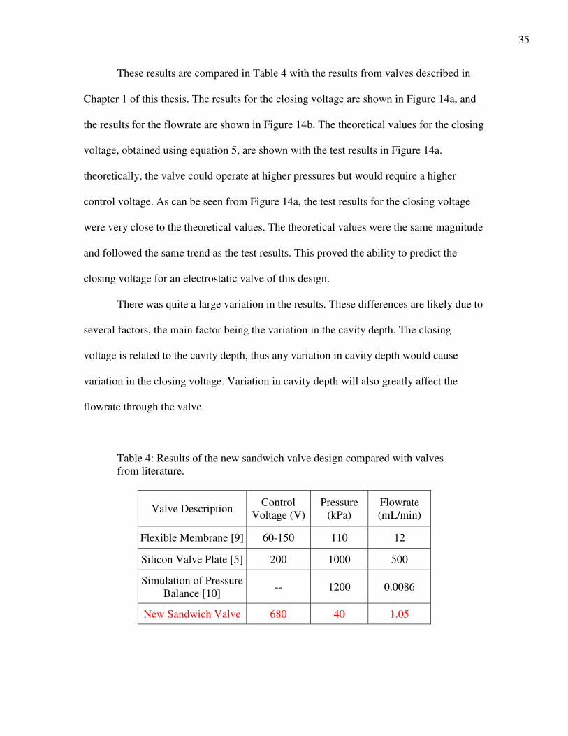
These results are compared in Table 4 with the results from valves described in
Chapter 1 of this thesis. The results for the closing voltage are shown in Figure 14a, and
the results for the flowrate are shown in Figure 14b. The theoretical values for the closing
voltage, obtained using equation 5, are shown with the test results in Figure 14a.
theoretically, the valve could operate at higher pressures but would require a higher
control voltage. As can be seen from Figure 14a, the test results for the closing voltage
were very close to the theoretical values. The theoretical values were the same magnitude
and followed the same trend as the test results. This proved the ability to predict the
closing voltage for an electrostatic valve of this design.
There was quite a large variation in the results. These differences are likely due to
several factors, the main factor being the variation in the cavity depth. The closing
voltage is related to the cavity depth, thus any variation in cavity depth would cause
variation in the closing voltage. Variation in cavity depth will also greatly affect the
flowrate through the valve.
Table 4: Results of the new sandwich valve design compared with valves
from literature.
Valve Description Control
Voltage (V)
Pressure
(kPa)
Flowrate
(mL/min)
Flexible Membrane [9] 60-150 110 12
Silicon Valve Plate [5] 200 1000 500
Simulation of Pressure
Balance [10] -- 1200 0.0086
New Sandwich Valve 680 40 1.05

36
0
200
400
600
800
1000
0 5 10 15 20 25 30 35 40 45
Pressure (kPa)
Vo
ltag
e (
V)
Test Results
Theoretical Values
0.0
0.5
1.0
1.5
2.0
2.5
0 5 10 15 20 25 30 35 40 45
Pressure (kPa)
Flo
wra
te (
mL
/min
) Test Results
(a) (b)
Figure 14: Results for valves tested with 6 µm parylene layer and 58 µm
cavity depth. (a) The closing voltage test results plotted with theoretical
values and (b) the flowrate test results.
The flowrate through a horizontal pipe is given by
L
pDQ
µ
π
128
4∆= (6)
where Q is the flowrate, ∆p is the pressure drop, D is the diameter of the pipe, µ is the
viscosity of the fluid, and L is the length of the pipe. Flowrate is a very sensitive function
of the diameter. A small variation in diameter would lead to a large variation in the
flowrate. The cavity depth was measured to have a depth of 58 µm ± 7%. Using equation
6 and assuming the cavity depth to be the diameter of the pipe and all other variable
constant, a 7% variation in cavity depth would lead to a 30% variation in flowrate. From
this analysis, much of the variation in the flowrate results can be attributed to the
variation in the cavity depth.

37
Other factors likely contributed to the variation in the results. When the device is
being assembled, the alignment between all the layers may be slightly different. If the
valve holes are lined up differently, there may be a difference in closing voltages and
flowrates. Any plastic deformation or contamination on the copper foil may also vary the
results. Additionally, the thickness of the parylene layer on the valve and on the copper
foil is known to vary slightly. This was likely due to the imperfect and statistical nature
of the parylene deposition.
The valve was also tested for the ability to control the flowrate through the valve
as a function of voltage. This was tested with a valve with a 58 µm cavity and an 8 µm
parylene layer. The results are shown in Figure 15. When the flowrate reached 0.0
mL/min in the graph, the flowrate had not completely stopped but it was below the range
of the flowmeter that was used. This graph shows that at higher pressures (above 40 kPa),
the valve may be able to function as a way to control gas flowrates.
Figure 15: Flowrate as a function of voltage. Valve tested had an 8 µm
parylene layer and an 80 µm cavity depth. These results show evidence of
stiction. The flowrate should be highest at 0 V, but this plot shows that is
not the case due to stiction when the voltage is off.

38
Dielectric Charging
During the tests it was observed that dielectric charging was occurring in the
valve. Dielectric charging is thought to occur when the high electric field causes electrons
or holes to be injected and trapped in the parylene layer. This can cause control voltage
drift or stiction of the valve [19-21]. Control voltage drift can be very high in parylene
insulated electrostatic actuators [22]. Figure 16 shows a drift in closing voltage over
actuation time. This graph shows the closing voltage for different pressures in the order
they were tested. When the valve was tested for the first time, the closing voltage at 25
kPa was found to be 500 V. After the valve had been actuated several times at different
pressures, the closing voltage at 20 kPa was found to be 900 V – higher than that for 25
kPa. This is evidence of control voltage drift due to dielectric charging.
Figure 16: Evidence of closing voltage drift caused by dielectric charging.
The closing voltage increased for lower pressures as the valve was used.
The valve had a 6 µm parylene layer and a 120 µm cavity depth.

39
Figure 15 shows stiction due to dielectric charging that occurred after the valve
has been actuated several times. Once a charge had started to accumulate in the dielectric
layer, there was a small attractive force in the valve even when the power supply is off,
which partially closed the valve. The valve required a small voltage from the power
supply to overcome the dielectric charge and reach a fully open state.
One solution that has been proposed to the problem of dielectric charging is to use
a bipolar control-voltage waveform [23]. This idea was tested on the valves presented in
this thesis. The valves were tested by finding the closing voltage for a valve at a given
pressure. The valves were then cycled on and off in 60 second increments, switching the
control voltage polarity with each actuation. Figure 17 shows these results compared
against the results of valves that did not have the control voltage polarity switched. These
results show that switching the control voltage polarity delayed the onset of dielectric
charging, but did not prevent it from occurring.
500
600
700
800
900
1000
0 5 10 15 20
Actuation
Clo
sin
g V
olt
ag
e (
V)
Figure 17: Valves tested for dielectric charging. This was done by
switching the control voltage with each actuation () and valves tested
without switching the control voltage polarity ().

40
Integration with Microfluidics
The electrostatic valve was tested for its use in a microfluidic system. The
microfluidic system was simplified to just a channel with an on-board valve for testing
purposes. The operation of the microfluidic system is described in Chapter 1 of this
thesis.
The electrostatic valve was connected with the microfluidic system by connecting
the valve outlet to the on-board microfluidic membrane valve. When the electrostatic
valve was off, the air flowed through the electrostatic valve and the pressure closed the
microfluidic membrane valve. When the electrostatic valve is on, the air pressure was
stopped and the fluid pressure can open the microfluidic valve. It was necessary to add a
vent in the connecting tube to release the pressure that is built up after the electrostatic
valve is closed. The vent was small enough that the pressure was still able to hold the on-
board valve closed while the electrostatic valve is open. Figure 18 is a diagram of the
electrostatic valve setup with the microfluidic system.
The electrostatic valve was successful in controlling the microfluidic system with
the following results: the fluid pressure was 12 kPa, the air pressure was 25 kPa, the
control voltage was 850 V, the actuation time to open the microfluidic valve was 12 s,
and the actuation time to close the microfluidic valve was 6 s. This demonstration
showed the electrostatic valve could be used with a microfluidic system to create a low-
cost, portable device.

41
Figure 18: Diagram of the electrostatic valve connected to the microfluidic
membrane valve. In this instance, the voltage is turned off and the air is
flowing through the electrostatic valve. This holds the membrane valve
closed, stopping the fluid flow.
Conclusion
Two valve parameters were varied in an effort to find the optimum valve
performance – parylene thickness and cavity depth. A design of experiments was
performed to test the best combinations of parameters. The valve with a 6 µm layer of
parylene with a 58 µm cavity depth was selected as the best valve, based on a balance
between a low closing voltage and a high flowrate. Several of these valves were tested
and the results showed the valve could operate up to 40 kPa with an average control
voltage of 680 V and an average flowrate of 1.05 mL/min. The variation between the

42
valves was higher than expected, likely due to manufacturing and assembly differences.
Tests also showed at higher pressures (above 40 kPa) the valve may be able to function as
a flowrate control valve.
It was observed that dielectric charging was occurring in the valves during testing.
Dielectric charging occurs when a high electric field causes electrons or holes to become
trapped in the dielectric layer. The dielectric charging caused a shift in the closing
voltage, as well as stiction in the valve. By alternating the polarity of the control voltage,
it was found that the onset of dielectric charging could be delayed.
Finally, the electrostatic valve was connected to a simplified microfluidic system.
The electrostatic valve was successful in controlling the fluid flow through the on-board
microvalve. This showed the feasibility of layering the electrostatic valve in line with a
microfluidic system to create a low-cost, portable system.

CHAPTER 5
CONCLUSION
Summary
This thesis presents a new electrostatic microvalve for the control of microfluidic
devices. These microfluidic devices currently use external solenoid valves, which are
expensive and bulky. This new electrostatic microvalve will be able to be layered below
the microfluidic system to allow for a compact, transportable system. The valve needed
to be easily, quickly, and inexpensively manufactured.
A sandwich assembly concept was used so each piece of the valve could be
quickly and independently manufactured. The design consisted of a valve plate made of
PMMA with chrome patterned on one side. Copper foil was used as the valve membrane.
Parylene C was deposited on both the valve plate and the copper foil to insulate the
electrodes to prevent shorting out. The bottom piece of the valve consisted of a cavity
etched in PMMA to allow the membrane to deflect and open the valve. An interface
device was made out of PMMA and used to interface the air line with the valve for
testing purposes. A CO2 laser was used to cut out the pieces of PMMA.
This design used the concept of a curved electrode, which kept the chrome and
the copper close together around the edges of the cavity and allowed the copper to deflect
in the middle of the cavity. This design allowed the electrostatic force to be high around

44
the edges where the electrodes were close together. This pulled the copper membrane
close around the edges, moving the electrodes closer together towards the middle of the
valve. In this way the copper foil could roll closed. A theoretical model was developed
that proved successful in predicting the closing voltage of the valve.
Two parameters of the valve were varied – parylene thickness and cavity depth.
Parylene thickness was tested at two different thicknesses, 6 µm and 8 µm. The cavity
depth was varied at three different levels, 16 µm, 58 µm and 105 µm. Different
combinations of these parameters were tested to find the best valve performance. The
valve was tested for operational voltage at different pressures and the flowrate through
the valve was measured. The valve was also tested to determine if it could function as a
flowrate control valve. Dielectric charging was observed and a possible solution was
explored. Finally the valve was connected to a simplified microfluidic system consisting
of a microchannel and a membrane and tested for its ability to control fluid flow.
There are several conclusions based on the results of the work presented.
• The sandwich concept using a curved electrode was effective in creating a low-
cost, easy-to-manufacture device.
• The best combination of parameters was a 6 µm layer of parylene with a 58 µm
cavity depth. This was based on a combination of low operational voltage and
high flowrate. Several valves with these parameters were tested and found to
function with a pressure up to 40 kPa with an average control voltage of 680 V
and an average flowrate of 1.05 mL/min. It is possible that the valve could
function at higher pressure but a higher control voltage would be required.

45
• The valve showed it may be able to function as a flowrate control valve at higher
pressures, i.e. greater than 40 kPa.
• Dielectric charging was a problem in these valves. This was evident in control
voltage drift or stiction of the valve. By switching the polarity of the control
voltage with each actuation, the onset of dielectric charging could be delayed.
• The electrostatic valve proved to be able to control the fluid flow through the
microchannel, which was a step towards integration of the electrostatic valve with
a microfluidic device.
Future Work
The valve presented in this thesis is the first step towards creating a valve array
system that can control the microfluidics on a lab-on-a-chip device. This valve was
effective in demonstrating the concept of sandwiching individually fabricated pieces to
create an inexpensive, easy-to-make microvalve. There are several aspects of the valve
that could be investigated as ways to improve valve performance.
Different copper foil thicknesses were examined, but these were much thicker
than the 10 µm foil that was successfully tested. Different foils with thicknesses between
6 µm and 14 µm may be acquired and tested. However, the cost of those copper foils may
prohibit its use in the valve. Further investigation can also be made into the parylene
layer thickness. There is a balance between the thickness of the dielectric layer, the
control voltage, and the electrostatic force. If a thinner parylene layer is used, the
electrostatic force will increase, so a lower control voltage can be used. However, the
valve will also break down at lower voltage. Contamination also may become an issue at

46
thinner dielectric layers. More work can be done to find the optimum parylene thickness
and control voltage.
Work also needs to be done on a solution to better control the dielectric charging.
Further research into dielectric charging has shown another possible solution is the use of
an AC supply voltage. There are reports that an AC supply voltage can greatly increase
the lifetime of electrostatic actuators [24]. Work is being done to test the valve with an
AC supply that would be able to operate the valve at high voltages.
The valve presented in this paper was a single valve on a large PMMA chip. A
proposed array of valves would contain 64 valves on a PMMA chip no larger than a
standard glass microscope slide, shown in Figure 19. Chrome can be patterned on the
PMMA using a shadow mask in the same way that was presented with the single valve.
The electrostatic valve array would be layered below the microfluidic layer to control an
entire microfluidic system. For the single valve tested in this paper, bolts were used to
hold the valve together. Work must be done to find a way to bond and package the valve
array so that it may be layered below the microfluidics. Such a system would allow for a
portable, low power system with integrated controls rather than external solenoid valves.
Figure 19: Array of 64 valves on a single PMMA chip. This chip is the
size of a standard microscope slide.

47
The uniqueness of the electrostatic valve presented in this paper is its materials,
manufacturing, its ability to function as an external valve controlling a pneumatic internal
valve, and the ability to layer an array of valves below a microfluidic system for
pneumatic control. Eliminating the external solenoid valves will increase portability,
decrease cost, and potentially make the entire device disposable. This electrostatic
microvalve has potential to improve the pneumatic control of lab-on-a-chip microfluidic
devices.

REFERENCES
[1] Hui Liu, R., Yang, J., Lenigk, F., Bonanno, J., and Grodzinski, P., 2004, “Self-
Contained, Fully Integrated Biochip for Sample Preparation, Polymerase Chain Reaction
Amplification, and DNA Microarray Detection” Analytical Chemistry, 76, pp. 1824-
1831.
[2] Vyawahare, S., Sitaula, S., Martin, S., Adalian, D., Scherer, A., 2008, “Electronic
Control of Elastomeric Circuits with Shape Memory Actuators,” Lab Chip, 8, pp. 1530-
1535.
[3] Oh, K.W., Ahn, C.H., 2006, “A Review of Microvalves,” J. Micromech. Microeng.,
16, pp. R13-R39.
[4] Zhang, C., Xing, D., Li, Y., 2007, “Micropumps, Microvalves, and Micromixers
within PCR Microfluidic Chips: Advances and Trends,” Biotechnology Advances, 25,
pp. 483-514.
[5] Messner, S., Schaible, J., Vollmer, J., Sandmaier, H., Zengerle, R., 2003,
“Electrostatic Driven 3-Way Silicon Microvalve for Pneumatic Applications,” The IEEE
16th
Annual International Conference on Micro Electro Mechanical Systems, IEEE,
Kyoto, pp. 88-91.
[6] Xie, J., Shih, J., Lin, Q., Yang, B., Tai, Y., 2004, “Surface Micromachined
Electrostatically Actuated Micro Peristaltic Pump,” Lab Chip, 4, pp. 495-501.
[7] Madou, M.J., 2002, Fundamentals of Microfabrication: the Science of
Miniaturization, 2nd
ed., CRC, Boca Raton, pp. 547.
[8] Zengerle, R., Richter, A., Sandmaier, H., 1992, “A Micro Membrane Pump with
Electrostatic Actuation,” Micro Electro Mechanical Systems, IEEE, Travemunde, pp. 19-
24.
[9] Goll, C., Bacher, W., Büstgens, B., Maas, D., Ruprecht, R., Schomburg, W.K., 1997,
“An Electrostatically Actuated Polymer Microvalve Equipped with a Movable Membrane
Electrode,” J. Micromech. Microeng., 7, p. 224-226.
49
[10] Quero, J.M., Luque, A., Franquelo, L.G., 2002, “A Novel Pressure Balanced
Microfluidic Valve,” 2002 IEEE International Symposium on Circuits and Systems,
IEEE, Phoenix, pp. II-588-II-591.
[11] Sasaki, H., Shikida, M., Sato, K., 2006, “A Force Transmission System Based on a
Tulip-Shaped Electrostatic Clutch for Haptic Display Devices,” J. Micromech.
Microeng., 16, pp. 2673-2683.
[12] Haji-Babaei, J., Kwok, C.Y., Huang, R.S., 1997, “Integrable Active Microvalve with
Surface Micromachined Curled-Up Actuator,” 1997 International Conference on Solid-
State Sensors and Actuators, TRANSDUCERS, Chicago, pp. 833-836.
[13] Sato, K., Shikida, M., 1992, “Electrostatic Film Actuator with a Large Vertical
Displacement,” Micro Electro Mechanical Systems, IEEE, Travemunde, pp. 1-5.
[14] Hirai, Y., Shindo, M., Tanaka, Y., 1998, “Study of Large Bending and Low Voltage
Drive Electrostatic Actuator with Novel Shaped Cantilever and Electrode,” International
Symp. On Micromechatronics and Human Science, IEEE, Nagoya, pp. 161-164.
[15] Saucedo-Flores, E., Ruelas, R., Flores, M., Chiao, J., 2003, “Study of the Pull-In
Voltage for MEMS Parallel Plate Capacitor Actuators,” A5.86, Material Research
Society Symposium Proc., LaVan, D. et al., eds., Materials Research Society, Warrendale,
782, p. 1-7.
[16] Asbury Graphite Mills, 2010, “Enhancing Conductivity in Polymers with Graphite
and Carbon,” http://www.asbury.com/Electrically-Conductive-Polymers.html.
[17] Zou, J.-F., Yu, Z.-Z., Pan, Y.-X., Fang, X.-P., Ou, Y.-C., 2002, “Conductive
Mechanism of Polymer Graphite Conducting Composites with Low Percolation
Threshold,” Journal of Polymer Science: Part B: Polymer Physics, 40, pp. 954-963.
[18] Product Data Sheet, Asbury Carbons, Inc., Asbury, NJ, http://www.asbury.com.
[19] Goldsmith, C., Ehmke, J., Malczewski, A., Pillans, B., Eshelman, S., Yao, Z., Brank,
J., Eberly, M., 2001, “Lifetime Characterization of Capacitive RF MEMS Switches,”
2001 IEEE MTT-S Int. Microwave Symposium Digest, IEEE, Phoenix, pp. 227-230.
[20] Yuan, X., Cherepko, S., Hwang, J., Goldsmith, C., Nordquist, C., Dyck, C., 2004,
“Initial Observation and Analysis of Dielectric-Charging Effects of RF MEMS
Capacitive Switches,” IEEE MTT-S International Microwave Symposium Digest, 3, pp.
1943-1946.

50
[21] Herfst, R.W., Huizing, H.G.A., Steeneken, P.G., Schmitz, J., 2006,
“Characterization of Dielectric Charging in RF MEMS Capacitive Switches,”
Proceedings of the 2006 International Conference on Microelectronic Test Structures,
IEEE, Austin, pp. 133-136.
[22] Yoa, T.-J., Walsh, K., Tai, Y.-C., 2002, “Dielectric Charging Effects on Parylene
Electrostatic Actuators,” The 15th
IEEE International Conference on Micro Electro
Mechanical Systems, IEEE, Las Vegas, pp. 614-617.
[23] Peng, Z., Yuan, X., Hwang, J., Forehand, D., Goldsmith, C., 2007, “Dielectric
Charging of RF MEMS Capacitive Switches Under Bipolar Control-Voltage
Waveforms,” 2007 International Microwave Symposium, IEEE, Honolulu, pp. 1817-
1820.
[24] Cabuz, C., 1999, “Dielectric Related Effects in Micromachined Electrostatic
Actuators,” 1999 Conference on Electrical Insulation and Dielectric Phenomena, IEEE,
Austin, pp. 327-332.