an electron microscope for the aberration-corrected era et al - ultrastem - ultramic 2008.pdf · an...
TRANSCRIPT

ARTICLE IN PRESS
0304-3991/$ - se
doi:10.1016/j.ul
�CorrespondiE-mail addre
Ultramicroscopy 108 (2008) 179–195
www.elsevier.com/locate/ultramic
An electron microscope for the aberration-corrected era
O.L. Krivanek�, G.J. Corbin, N. Dellby, B.F. Elston, R.J. Keyse, M.F. Murfitt,C.S. Own, Z.S. Szilagyi, J.W. Woodruff
Nion Co., 1102 8th Street, Kirkland, WA 98033, USA
Abstract
Improved resolution made possible by aberration correction has greatly increased the demands on the performance of all parts of high-
end electron microscopes. In order to meet these demands, we have designed and built an entirely new scanning transmission electron
microscope (STEM). The microscope includes a flexible illumination system that allows the properties of its probe to be changed on-the-
fly, a third-generation aberration corrector which corrects all geometric aberrations up to fifth order, an ultra-responsive yet stable five-
axis sample stage, and a flexible configuration of optimized detectors. The microscope features many innovations, such as a modular
column assembled from building blocks that can be stacked in almost any order, in situ storage and cleaning facilities for up to five
samples, computer-controlled loading of samples into the column, and self-diagnosing electronics. The microscope construction is
described, and examples of its capabilities are shown.
r 2007 Elsevier B.V. All rights reserved.
PACS: 07.78.+s; 42.15.Fr; 41.85.�p; 68.37.Hk; 06.60.Sx
Keywords: Aberration correction; STEM design; Sample stage; HAADF imaging; EELS
1. Introduction
Correction of electron-optical aberrations is a field witha 60-year history [1,2], which has blossomed in the last 10years. Aberration correctors have significantly improvedthe performance of scanning electron microscopes (SEMs)[3], transmission electron microscopes (TEMs) [4] andscanning transmission electron microscopes (STEMs)[5–7]. Aberration-corrected electron microscopes are nowfinding their way into mainstream usage in large numbers.The attainable STEM resolution has improved by about2.5�, and the current available in a given-size small probehas increased by about 10�. Further major improvementsare expected when a new generation of instruments such asthe one described here come fully on-line.
The microscope column itself, on the other hand, has notimproved to a similar extent. The electron guns, roundlenses, objective lens (OL) polepieces, sample stages, and
e front matter r 2007 Elsevier B.V. All rights reserved.
tramic.2007.07.010
ng author.
ss: [email protected] (O.L. Krivanek).
detectors available in present-day instruments are quitesimilar to the best available 20–30 years ago. This isexemplified by the Topcon 002B, introduced in 1986, whichfeatured double-winding round lenses able to maintainconstant heat output even as their magnetic excitation waschanged, a condenser-OL with spherical aberration coeffi-cient Cs=0.4mm and chromatic aberration coefficientCc=0.8mm (at 200 kV), an illumination system consistingof five lenses, toroidal deflectors with minimized hysteresis,and a reasonably stable side-entry sample stage [8,9]. It wasa well-rounded instrument, optimized for 2 A resolution,which was the norm for the top instruments of its day.Even the best non-aberration corrected dedicated STEM,the 300 kV VG HB603 [10], did not manage to improve onmany of these characteristics.The lack of progress in microscope design is surprising in
view of the fact that aberration-corrected instruments arenow approaching 0.5 A resolution, and that atomic-resolution elemental mapping by electron energy-lossspectroscopy (EELS) and energy-dispersive X-ray spectro-scopy (EDXS), which place serious demands on long-term

ARTICLE IN PRESSO.L. Krivanek et al. / Ultramicroscopy 108 (2008) 179–195180
stability, are about to become established techniques. Thecontinued use of aging design elements has resulted in asituation whereby today’s highest-performance micro-scopes are so sensitive that the designers of the micro-scopes’ foundations need to be concerned about thepounding of ocean waves on a shore 30 miles distant[11]. The microscopes need to be housed in custom-builtlabs with special vibration-free foundations, thoroughsound shielding, minimized stray magnetic fields, and airtemperature that is kept constant to within 0.1 1C [11,12].Even with these precautions, they remain sensitive toadventitious disturbances such as pressure changes due todoors opening and closing, and the low frequency magneticfields due to passing trucks [12].
At Nion, we have decided to adopt a different approach:design an entirely new instrument in a way that takes theincreased demands into account right from the start. Otherfundamental goals of the design were to give the instrumentas much flexibility as possible, and at the same time toautomate its basic operation so that even novice micro-scopists can use the instrument near its full potential. Onemore very important goal was to make the microscopecompletely computer-controlled, so that its full function-ality, including sample exchange, would be available toremote users over the Internet.
2. Design overview
The new microscope has been developed on two parallelbut converging paths. Its electron-optical column wasdesigned, built, and tested using a 100 kV VG cold fieldemission gun (CFEG) as the electron source, and is nowfully functional. At the same time, a 200 kV CFEG is beingdeveloped separately. This gun is now fully built up, but itis still being tested. It will be the subject of a separatepublication.
Fig. 1a shows the new column, and Fig. 1b shows itsschematic cross-section. The VG 100 kV gun has a verygood vacuum (typically in the low 10�11 Torr range),stability such that the emission current from a freshlycleaned tip takes 40min or more to decay to 50%,brightness 41013A/(m2 sr) at 100 kV, and energy spread�0.3 eV. We have used the basic gun plus its high-voltagetank, but replaced the control electronics with a digitaldesign that is computer-controlled, and water-cooled forimproved stability.
Electron-optically, the new column starts with a pair ofdeflectors for steering the beam coming up from the gun,and continues with three round condenser lenses, aquadrupole–octupole C3/C5 corrector, a quadrupole tripletcalled quadrupole lens module (QLM) for coupling thecorrector electron-optically to the OL, a lower OL windingmodule, sample stage/OL polepiece module, an upper OLwinding module, four round projector lenses, and adetector column that includes several detectors and otherdevices: a high-angle annular dark-field (HAADF) detec-tor, a pneumatically controlled beam stop that can be
inserted when recording diffraction patterns, medium angleannular dark-field (MAADF) detector, bright field (BF) de-tector, a quadrupole/octupole module called quadrupole–octupole coupling module (QOCM) for optimizedcoupling of inelastically scattered electrons into an electronenergy loss spectrometer, a 1k� 1k fast read-out CCDcamera for Ronchigram, diffraction pattern and imageread out, an EELS entrance aperture and finally anelectron energy-loss spectrometer, typically a GatanEnfina.The column has been designed for 200 kV operation.
Operation at 100 kV and lower voltages is possible andactually involves several advantages, such as reducedknock-on damage in light element materials. When thecolumn is interfaced to the VG 100 kV CFEG, it outper-forms the aberration-corrected version of the VG column(VG condensers, OL and sample stage, plus Nion Cs
corrector) in essentially all respects.The column is entirely modular. All the modules are
275mm in diameter and either 60mm or a multiple of60mm in height. They all have the same mechanicalinterface, and can therefore be stacked in practically anyorder.Each module of the Nion column has integral double
m-metal magnetic shielding. Measured sensitivity to straymagnetic fields at 100 kV is 0.6 A r.m.s. probe movementper 1mG r.m.s. of uniform 60-cycle fields. Measurement ofsensitivity to localized AC fields showed the shielding to bethe weakest at the top of the VG gun. We expect that withNion’s own CFEG, the sensitivity will be reduced further.In addition to the lens and detector modules listed
above, there are also three pumping/aperture modules.These modules provide several different functions, asneeded at their particular locations: a vacuum connectionto a pump, a pneumatically controlled gate valve, anaperture that can be shifted mechanically and electrically,an electrostatic beam blanker, and an in-column m-metalshield that decouples the magnetic excitation of lensesabove and below the shield. The modules have the standardmechanical interface, and can be placed anywhere in thecolumn.In the present design, the first pumping/aperture module
is placed between the first and second condenser lenses. Itcontains a vacuum connection to the condensers’ ionpump, a pneumatic gate valve that can isolate the gun fromthe rest of the microscope, an aperture and a beam blanker.A second pumping module is placed between the upper OLwinding and the first projector lens. It contains a vacuumconnection to the projectors’ ion pump and a magneticshield that eliminates small magnetic cross-talk that wouldotherwise occur between the projectors and the OL. A thirdpumping module is placed between the last projector lensand the detectors. It provides a vacuum connection to thedetectors’ ion pump and a pneumatic gate valve that canisolate the detectors from the rest of the microscope,for operations such as changing a scintillator or servicingthe EELS.

ARTICLE IN PRESS
Fig. 1. (a) The new column and (b) schematic cross-section of the column.
O.L. Krivanek et al. / Ultramicroscopy 108 (2008) 179–195 181
The modularity of the column means that differentconfigurations can be adopted quickly and easily.For instance, we first assembled the microscope with onlytwo condenser and two projector lenses, but changed thisto three condensers and four projectors for greaterflexibility in adjusting the angular range and current ofthe probe, and in forming diffraction patterns and CTEMimages. Further lenses and other modules can be addedlater, even after installation. Equally importantly, thesample stage module, which follows the same modularscheme, can be removed and replaced by another one andthe microscope can be back in operation typically in lessthan one day.
2.1. Round lenses
Each one of the column’s round condenser and projectorlenses contains an interchangeable polepiece whichallows its minimum focal length (fmin) to be chosen asneeded. To suit the different requirements placed on eachparticular lens, we presently use three types of polepieces: asymmetric polepiece with fmin ¼ 15mm, a smaller-gapsymmetric polepiece with fmin ¼ 4mm, and an asymmetricpolepiece with fmin ¼ 4mm. To obtain the best possibletolerances on the alignment of the top and bottompolepieces, we machine them in the same way that OLpolepieces are made for most other microscopes: thepolepieces are first joined together by a non-magnetic
spacer, and the final machining is carried out only on thejoined assembly.Each lens also contains two magnetic deflectors, which
ensure that the incoming beam is sent into the lens alongthe lens axis, and is then passed onto the next opticalstage as needed by that stage. This gives the whole columnthe same alignment flexibility as if each lens had mecha-nical ‘‘shifts’’ (shifting the lens sideways) and ‘‘tilts’’(shifting one polepiece mechanically w.r.t. the other),but without the inconvenience and tendency to driftinherent to mechanical shifters. Because of the goodalignment of the upper and lower polepieces attained bymachining them together, the optical axis of the lens istypically found to coincide with the mechanical axisof the whole column to better than 0.51. This means thatthe magnetic fields needed to reach proper alignment arequite weak, and the deflectors do not make a majorcontribution to the overall stability budget for the wholemicroscope.All the round lenses have double windings, wound in an
interleaved fashion. The lenses are supplied by twoindependent power supplies such that the power dissipa-tion is held constant at all the different magnetic excitationsettings. This means that changing the lens setting does notchange its heat output, and does not result in thermal driftthat could otherwise affect the microscope stability for tensof minutes after the change. Because the OL has a lowerand an upper winding, each one of which is double-wound,

ARTICLE IN PRESSO.L. Krivanek et al. / Ultramicroscopy 108 (2008) 179–195182
the OL uses a total of four windings and is powered by fourseparate current supplies. The total cross-section of its lenscoils has made the total power dissipated in the OL lessthan 150W at 100 kV.
The three condensers used in our standard column allowthe illumination angle to be varied widely, from o1mradsemi-angle to440mrad. The beam current can be adjustedat the same time by changing the demagnification of thefield-emission source. The whole adjustment range isavailable using just a single virtual objective aperture(VOA), typically of 30 mm diameter. Fig. 2 shows how thisis done. The gun lens (C0) is typically run at constantexcitation such that it produces a crossover near the gun’sdifferential pumping aperture (but it could be used to shiftall regimes towards higher or lower probe currents). C1
then becomes the lens that sets the probe current. When itproduces a crossover far from the VOA, smaller beamcurrent and larger source demagnification (i.e., betterresolution but noisier data) result. This is shown inFig. 2a. When the crossover produced by C1 moves closerto the VOA (Fig. 2b), a larger beam current, less sourcedemagnification, and bigger probes result. C2 is thenadjusted to give the same beam diameter in C3 as for thehigher demagnification mode, and C3 is adjusted toproduce the same beam divergence (typically a parallelbeam). For the two modes, the beam arriving at thecorrector then appears to originate from the same place inthe column. It also has the same diameter (and hence thesame convergence angle at the sample), but different sourcedemagnifications.
In practice, several different source demagnificationmodes are made available to the user, to make it possibleto select the right probe current to suit the application athand. The switching between the modes is accomplished ina few seconds, and the probe generally moves by less than10 nm relative to its previous location. Because C1 to C3 areall run in the constant-power mode, no long-term driftresults from the switchover.
electrical centering for VOA
to corrector
C3
C2
VOA
C1
DPA
C0 (gun lens)
Fig. 2. Different probe setup regimes made possible by the three
condensers: (a) small, convergent probe with large source demagnification,
(b) small convergent probe with less source demagnification (and hence
bigger probe current) and (c) larger but more parallel probe with the same
beam current as (b). Note that the virtual objective aperture remains the
same for all the regimes.
To decrease the convergence angle of the probeilluminating the sample, as for instance needed forparallel-beam diffraction and TEM imaging, the diameterof the beam sent up to the corrector needs to be decreased.This is done by adjusting C2 so that the crossover itproduces is shifted closer to C3, and adjusting C3 so thatthe beam coming out of it is again nearly parallel. This isshown in Fig. 2c. Leaving C1 unchanged leaves the beamcurrent the same as for the more convergent probe setup(cf. Fig. 2b), and of course C1 can also be changed to adjustthe beam current as needed.The OL is a symmetric, Riecke-Ruska type [13]
condenser-OL. Our standard high-resolution polepiecehas a gap of 4mm and a bore of 1.5mm, and is thereforebetter optimized for low chromatic aberration (Cc, whichwe do not correct in this column), than for sphericalaberration (Cs, which we do correct). Its focal length isf ¼ 1.5mm for both the pre-field and post-field parts, itscalculated aberration coefficients are Cs ¼ 1.1mm,Cc ¼ 0.95mm at 100 kV, and Cs ¼ 1.0mm, Cc ¼ 1.1mmat 200 kV. The polepiece is a part of the sample stagemodule, and is therefore changed whenever the samplechamber is switched with another one.The four projectors give a wide range of camera lengths
for diffraction pattern recording, from o10mm to 41mon the main CCD camera. The diffraction patterns areproperly focused, i.e. the pattern appearing on the CCDdoes not shift or grow fuzzy when the probe is scanningover a large sample area. The four projectors also allowconventional TEM (CTEM) imaging (which is not aberra-tion corrected in our standard column, whose mainemphasis is on STEM), at magnifications of up to400,000�. Even without the addition of further roundlenses (which is easy to do with our column), both thecamera length and the magnification ranges can beextended further by the use of the pre-CCD QOCM.Just like in a regular CTEM, high-magnification CTEM
imaging in the Nion column requires the first projector (P1)to run near its maximum strength, and the OL to project afocused image of the sample into the front-focal plane ofP1. The OL excitation and sample height used for CTEMimaging turn out to be close to the optimum setup for theformation of distortion-free diffraction patterns extendingup to the maximum angles allowed by the OL’s upper bore,and could therefore be used as the starting point fordiffraction modes and for coupling into the EELS.However, the maximum angle that can be collected onthe HAADF detector can be increased by about 20% if thepost-sample part of the OL is underfocused slightly so thatthe real image of the sample produced by the OL movesbeyond P1. This means that the sample needs to be raisedby a small amount (about 5 mm) and the OL excitationslightly weakened. This constitutes our standard mode ofsetting up the projector lenses for STEM signal detection.In this standard regime, P1 is weakly excited so that it
focuses on the diffraction pattern in the back-focal planeof the OL. The regime amounts to coupling into the

ARTICLE IN PRESSO.L. Krivanek et al. / Ultramicroscopy 108 (2008) 179–195 183
projectors with an angular compression factor of about 150due to the OL alone. Under the typical STEM detectionsetup (see Section 2.3), the projectors reduce this compres-sion to about 10� for the beam leaving P4, and also allowthe compression (i.e., the camera length of the diffractionpattern) to be varied while the diffraction pattern staysin focus.
A critical consideration when the projector column is runin this way is that even small changes in the sample height,of the order of a few mm, change the regime considerably. Itis therefore important that the sample height inside the OLbe controlled with precision better than about 100 nm.Thisis accomplished very competently by the (X, Y, Z, a, b)five-axis stage described in Section 2.4.
The column can also be run with the OL excitation set tozero. This makes the probe about 100� less convergentthan when the OL is on, and thus about 100� larger. Theavailable camera lengths also increase by about 100�. BFand DF images can nevertheless still be formed. The modeis very useful for low magnification ‘‘survey’’ imaging, atfields of view up to about 1mm, and it may also be usefulfor studying long-range order by very high-resolutiondiffraction, at camera lengths of 10m and more. Becausethe OL coils are double-wound, the magnetic field of thelens is turned off without any change in its overall heating,thus eliminating long-term drift that would have resultedwith a single-winding OL.
2.2. Aberration corrector
The aberration corrector is our third-generation design.It has been described in detail previously [14–16]. It uses 12rotatable quadrupoles and three combined quadrupole–octupoles. The three quadrupole–octupoles correct third-order axial aberrations, similar to our second-generationdesign [5,6]. Unlike in the previous design, in the newdesign the quadrupole–octupoles are precisely imaged intoeach other, and the third quadrupole–octupole is imagedinto the coma-free plane of the OL. The magnification isdifferent in different transverse directions. There is a roundbeam in the first quadrupole–octupole, an elliptical beamelongated in one transverse direction in the second one,
Fig. 3. Axial (a) and field (b) trajecto
and an elliptical beam elongated in the perpendiculardirection in the third one.The optical conditions described above allow third-order
axial aberrations to be corrected without introducingcombination fifth-order axial aberrations. A quadrupolequadruplet (4 quadrupoles) is needed for imaging eachquadrupole–octupole into the next, a quadrupole triplet isused to couple the beam arriving from the condensers intothe bottom quadrupole–octupole, and finally a quadrupolequadruplet is used to couple the third quadrupole–octupoleinto the OL. One of the final quadrupoles is a part of thecorrector; three more are located in the QLM placedbetween the corrector and the OL.The corrector is 30 cm long and therefore amounts to a
quintuple-height module. Its magnetic polepieces are madeand aligned to each other with better than 10 mm precision.The axial trajectories through the corrector are shown inFig. 3a. By combining octupoles with quadrupoles, we areable to operate in a regime in which the beam is relativelynarrow everywhere except in the quadrupole–octupolesthemselves. This is precisely the general arrangement thatminimizes the contribution of the corrector to the overallchromatic aberration budget [16]. In our particular case,the Cc contribution of the corrector amounts to 0.21mm.Fig. 3b shows the field trajectories. They demonstrate
how the corrector’s quadrupole–octupoles are imaged intoeach other, and the last quadrupole–octupole is imagedinto the coma-free plane of the OL. In reality, this lastimaging is slightly misadjusted. The resultant combinationC5 [15,16] is used to null the C5 inherent to the opticalsystem, i.e. to correct the principal fifth-order sphericalaberration. This is what allows the corrector to nullfifth order aberrations in addition to the third-orderaberrations.Each quadrupole layer of the corrector needs four
current supplies: one each for its ‘‘normal’’ and ‘‘skew’’quadrupoles, plus one each for its X and Y dipoles. Thequadrupole–octupole layers need five supplies. The correc-tor therefore uses a total of 48+15=63 power supplies.A further 12 supplies are used in the QLM just above thecorrector, meaning that 75 high-stability current suppliesare required by this part of the column.
ries through the C3/C5 corrector.

ARTICLE IN PRESSO.L. Krivanek et al. / Ultramicroscopy 108 (2008) 179–195184
The large number of elements and power supplies hasgiven the corrector a large number of degrees of freedom,both for using different types of trajectories to attain thedesired correction, and even more so for the different waysthe corrector can be misaligned. At the same time, theprecision with which the corrector needs to be set up hasgone up considerably compared to C3-only correctors. Thishas resulted in a new paradigm, in which the humanoperator is no longer able to manually bring up thecorrector trajectories or perform a subsequent fullre-alignment, both of which could still be done byan experienced operator using our second-generationcorrector.
To overcome this limitation, we have developed softwarethat analyzes the beam trajectory through the correctorlayer-by-layer, and iteratively brings it in into agreementwith the desired trajectories predicted by the computer. Thesoftware automatically compensates for linear sample driftduring the measurement. It requires between 5 and 30minper iteration, depending on how close or far to the desiredsolution the corrector is. 10–15 iterations are typicallyrequired during the initial bringup procedure to set all theaberration coefficients, including fourth- and fifth-orderones, to be smaller than the desired limits. Fortunately, theresultant setup is found to be quite stable, and the fullinitial alignment procedure does not need to be repeated
Fig. 4. Schematic cross-section through the detector section of the column. T
detectors, the CCD camera, and the EELS aperture can all be inserted/remov
except if the corrector has been disassembled and put backtogether again.The day-to-day ‘‘touch-up’’ alignment typically only
needs to tune aberrations of third and lower orders, and isperformed in a few minutes.
2.3. Detectors
The detector system is designed to give a large degree offlexibility and automation. It is able to detect severalsignals simultaneously, and to select which signals will bedetected purely under software control. A cross-sectionthrough the detector system is shown in Fig. 4.Just like the main column, the detector part of the
microscope column is modular. However, the detectormodules are only 120mm in diameter. This brings thephotomultiplier tubes (PMTs) closer to the scintillators,helping to optimize their coupling efficiency. In thestandard configuration of the system, there are twoseparate annular STEM detectors that use a scintillatorcoupled to a PMT.STEM detector I is located in front of the quadrupole–
octupole coupling module (QOCM), the STEM detector IIafter the QOCM. The column section above the QOCMalso houses the 1k� 1k CCD camera and further an EELSentrance aperture.
he scintillators of the HAADF detector/beam stop and the BF/MAADF
ed into/from their on-axis positions using pneumatic mechanisms.
ARTICLE IN PRESSO.L. Krivanek et al. / Ultramicroscopy 108 (2008) 179–195 185
Detector I has three working positions: (i) high-angleannular dark-field (HAADF) detector; (ii) beam-stop forobscuring the (0, 0) spot in quasi-parallel-beam diffractionpatterns; and (iii) both the HAADF and the beam stopremoved, for unobstructed recording of Ronchigrams anddiffraction patterns by the CCD.
Detector II also has three working positions: (i) medium-angle annular dark-field (MAADF) detector, (ii) brightfield (BF) detector, (iii) both detectors removed from thebeam for unobstructed Ronchigram and diffractionpattern recording by the CCD.
The scintillator part of the STEM detectors usesinterchangeable modules that include the scintillator, ascintillator liner consisting of a thin metallic tube thatshields the non-conductive scintillator hole, and a para-bolic mirror that reflects the generated photons towards thePMT. The modules are fastened into a scintillator carriercapable of holding two such modules, and are movedpneumatically into an on-axis position that faces the PMT.A fine mechanical adjustment is provided for centering thescintillators on the detector module’s axis. The scintillatorsthemselves are made of single-crystal YAP. About 2000photons are generated by each incident electron, and about100 of the photons reach the cathode of the PMT. Thisallows for very efficient signal detection. It also meansthat single electron counting could be readily implementedfor very weak signals such as those used in low-dosebiological work.
The CCD camera is mounted just above STEM detectorII. It uses a 1k� 1k CCD chip with a separate read-outarea and a 15MHz read-out rate. The whole imagedetected by the CCD is first shifted into the read-out area,and then read out. The shift is performed in less than 1ms,and no beam shuttering is therefore required. Up to 15 full-size images can be recorded and displayed per second, orup to 30 images that are binned to 512� 512. At the sametime, recording times of a few seconds can be used for timeintegration of weak features. The chip uses anti-bloomingtechnology, which is useful when recording spot diffractionpatterns. The pixel size is 14� 14 mm2, and the chip is fiber-optically coupled to a P32 powder scintillator. The cameramoves in-and-out using a bellows seal and pneumaticactivation. The CCD chip and other temperature-sensitivecamera components can be removed from the columnwithout breaking the vacuum, which needs to be donewhen baking the whole microscope.
Above the CCD, there is a 4-position EELS entranceaperture, also pneumatically controlled, and finally anelectron energy-loss spectrometer. The Gatan Enfina,which is able to record spectra at a fast rate with goodDQE and a wide range of dispersion values, and hasextensive software for spectrum analysis and spectrum-imaging, is used.
The optics of the Enfina has some known limitations: itlacks an electrical adjustment for one of the threeimportant second-order spectrum aberrations, and it hasno third-order aberration adjustments. This is not a serious
limitation for normal TEM EELS performed at around1 eV energy resolution with a typical 2mm entranceaperture. However, with a CFER, energy resolution betterthan 0.4 eV is readily achievable, and the resolution lossdue to the spectrometer should be minimized, ideally too0.1 eV. At the same time, entrance beams of 2–3mmdiameter are needed to avoid having to ‘‘compress’’ theangular distribution excessively, as this would result in toomuch sensitivity to probe movement, and it could also leadto the Cs of the OL post-sample field affecting the spectrumresolution in a major way.In the Nion microscope, these limitations are overcome
by the QOCM. This module uses three quadrupole–octu-poles to perform the following functions:
(a)
Adjust the height of the entrance crossover seen by thespectrometer. This has the effect of changing thesecond-order spectrum aberration that is not electri-cally adjustable by the Enfina itself. Together with thetrim coils for the other two second-order aberrationsprovided by the Enfina, the system is therefore able totune all the second order spectrum aberrations.(b)
Provide electrical adjustments for all four third-orderspectrum aberrations.(c)
Provide an extra lens for modifying the camera lengthof the diffraction patterns or the magnification of theimages to be recorded by the CCD camera. This lenshas the advantage that it allows the camera length ofthe diffraction pattern at the CCD to be varied relativeto the camera length on the HAADF detector. Thismakes it possible to expand the inner cone admitted bythe HAADF scintillator so that it covers nearly thewhole CCD, which is useful for higher-resolutionviewing of Ronchigrams. It also allows the cameralength on the BF detector to be changed relative to theHAADF detector, which is useful when recordingHAADF and BF images simultaneously.Typical operating modes of the detector setup are shownin Table 1. The gaps between shown ranges are typicallydue to scintillator liners. Other collection angle combina-tions can be obtained by adjusting the round projectorlenses, the QOCM, or by replacing the modular scintilla-tors by ones with different diameters.
2.4. Sample stage
The sample stage is a fundamentally new design. Itemploys radial symmetry in such a manner that when thetemperature of the whole stage changes uniformly, there isno change in the sample position, to first order. This isillustrated in Fig. 5, which shows that the balls that drivethe stage push against surfaces that are parallel to thermalexpansion directions. Provided that the sample cartridgeand the cartridge housing are made from the same materialas the stage ring, thermal expansion therefore results inno shift of the sample relative to the microscope axis.

ARTICLE IN PRESS
Table 1
Different detection modes of the microscope
Detector name Mode name
HAADF
+EELS
HAADF
+MAADF
+EELS
HAAD
+BF
HAAD
+CCD
(Ronchi-gram)
CCD
(diffraction pattern)
CCD
(TEM image)
HAADF (det. I) 80–240 80–240 80–240 80–240 – –
MAADF (det. II) – 40–60 – – –
BF (alt. det. II) – – o40a – –
CCD – – – 0–60 10mmpCL p1mb 100�pmagp400k� c
EELS 0–60 0–30 –
Illum. apert. (a) p50 p30 p50 Any
The table lists the half-angles (in mrad) intercepted by each particular detector. The angular radius of the illumination aperture appropriate to each mode
is also shown.aDefined by an aperture placed in front of the BF detector and the QOCM setup. Typically about 3mrad.b10mm CL corresponds to a 100mrad half-angle falling 1mm from the center of the CCD (and therefore being usable by the EELS, which typically
operates with a 2.5mm diameter entrance aperture). 1m CL corresponds to77mrad field of view on the CCD.cOL is off for mago3k� . The top magnification can be extended to 41M� by using the QOCM in addition to the projectors.
Fig. 5. Schematic illustration showing that uniform thermal expansion of
the stage has no first-order effect on the position of the sample.
O.L. Krivanek et al. / Ultramicroscopy 108 (2008) 179–195186
In contrast, side-entry stages are very sensitive to changesin temperature, as anyone who has used a side-entry stageof a microscope sited in a room with poor temperatureregulation can attest.
A major design aim for the stage was to eliminatefriction, dead travel and backlash as much as possible.Accordingly, the X, Y and Z stage drives only do a total offour motion transfers each, from one moving part onto thenext, in order to couple the rotation of their stepper motorsto the motion of the sample. The drives employ onlyelastic hinges and pre-loaded ball bearings to achieve
nearly zero-friction motion with no backlash or hysteresis.This is all different from traditional stage drive designs,which typically do many more motion transfers (e.g., theX-drive of the Topcon 002B does seven transfers), severalof which are not backlash-free.A potential weakness of friction-free designs like ours is
that without friction, energy of vibrations does not readilydissipate, which could make the stage vibration-prone. Wehave overcome this by providing the stage with adjustablevibration dampers, and by making the stage lightweightand stiff. (Higher resonant frequencies make it harder forvibrations to couple into the stage efficiently, and makethem dissipate faster.) The result is that the lowestmeasured resonant frequency of the stage is 950Hz. Withthe dampers properly adjusted, the stage ‘‘glides’’ into anew position on a time scale of about 0.5 s, and has goodmechanical stability even in a fairly noisy acousticenvironment.As described in Section 2.8, stepper motors for the X, Y
and Z drives have about 3.5 million addressable stepscovering the motion range. The range is 71.5mm (for X
and Y) and 71mm (for Z). This means that if the stagewere completely friction-free, the steppers would allowsmallest motion steps of about 1 nm in all three directions.Working with the stage shows that the smallest actual X
and Y steps are about 2 nm. This means that we were rathersuccessful in eliminating mechanical friction, but notcompletely so. The sample height Z can be changed withabout 5 nm precision and the Z-motion causes less than20 nm of sideways (X, Y) motion (for defocus changeso1 mm). The sample can therefore be brought close tocorrect focus mechanically, which has the great advantagethat the pre-sample and post-sample optical conditionsremain unchanged.The double-tilt cartridge designed for the stage features a
new mechanism with two tilt axes that are at 901 to each

ARTICLE IN PRESSO.L. Krivanek et al. / Ultramicroscopy 108 (2008) 179–195 187
other and 451 to the principal cartridge axis. It achieves7301 tilt in any direction (in a 4mm polepiece gap). Thesame stepper motor mechanisms are used for the tilts as forthe X, Y, Z drives, and have a total number of addressablemotor positions of about 3 million for the 7301 tilt range.The cartridge uses miniature ball bearings for friction-freeoperation, but the motion coupling is less direct and lessfriction-free than for the X, Y, Z drives. The result is thatthe cartridge has demonstrated reproducible tilt steps ofabout 0.5mrad (0.031). This corresponds to an atomat the top of a 1000 A thick sample moving sideways by0.5 A w.r.t. an atom at the bottom of the sample, andshould be more than adequate for nearly all microscopyneeds.
A 5-axis stage (X, Y, Z, a, b) with the above degree ofmechanical precision can be readily computerized toprovide eucentric tilting along two axes [17]. The appro-priate software is being developed and tested. One of thecapabilities of the software will be ‘‘point-and-click
Fig. 6. (a) The storage magazine, loaded up with three sample cartridges. (b
tilting’’: while looking at a live image of a diffractionpattern, the user will be able to click on a location in thepattern, whereupon the sample will be tilted so that thedirection corresponding to the clicked location becomesparallel with the beam direction. This will mean that whenthe center of a zero-order Laue zone visible in a single-crystal diffraction pattern is clicked on, the correspondingzone axis will become aligned with the microscope beamaxis. The software will also automatically compensate forany changes in X, Y, Z positions that will result from tiltingthe sample, and the user will be presented with a newdiffraction pattern from the same area, at the same heightin the polepiece, but with the new tilt.
2.5. Sample storage/airlock
Up to five sample cartridges can be loaded into themicroscope at the same time, evacuated, and then insertedinto the in-column (observation) position under computer
)–(e) Schematic diagrams of the sample storage and loading mechanism.

ARTICLE IN PRESS
Fig. 7. Schematic diagram of the scan and magnification parts of the scan/
magnification/acquisition unit.
O.L. Krivanek et al. / Ultramicroscopy 108 (2008) 179–195188
control. The magazine that holds the cartridges and thedifferent working positions of the storage/loading mecha-nism are shown in Fig. 6.
The magazine (Fig. 6a) is normally stored in a ‘‘storagechamber’’, which is attached to the side of the microscopecolumn. The upper part of the chamber serves as anairlock. It is isolated from the rest of the storagechamber whenever the receptacle for the cartridge maga-zine is in its topmost position (Fig. 6b). The magazine isinserted into the airlock manually, the lid (which hastwo Viton O-rings, differentially pumped) is closed,and the rest of the evacuation/insertion sequence isperformed under computer control. The first part of theevacuation is done by a turbo pre-pumping station, withthe magazine in the topmost position. While the newlyinserted magazine is still in the airlock and being pumpedby the turbo, it can be baked at 120–140 1C, also undercomputer control. It is then lowered into the storagechamber proper, where the pumping is provided by a30 l/s ion pump. From there, sample cartridges areindividually selected (Fig. 6c) and moved into the samplestage by a pneumatically driven arm (Fig. 6e). While themagazine is moved up and down, the exchange arm (withor without a sample on it) is fully retracted into a‘‘preparation chamber’’ to stay free of the magazine(Fig. 6d). Two ports are provided on the preparationchamber for optional ion guns (or other attachments) witha line-of-sight towards the sample, for sample cleaningand/or thinning.
The system allows a magazine with five cartridges to beinserted into the microscope and evacuated, and thesamples to be cleaned by heating or other means. The usercan then select any one of the five samples for observation,under computer control. Five samples should typically beenough for an experimental session. While the session isproceeding, a second magazine can be prepared with itscomplement of samples. The magazines can then beswapped, and the next user can start operating themicroscope in less time than if all the previous sampleshad to be offloaded first from their cartridges to makeroom for new samples.
2.6. Scanning and data acquisition system
The Nion scan/magnification/acquisition system is de-signed to drive four layers of scan coils, as required forcomplete freedom in scanning and descanning the probe,vary the magnification as required, and digitize severalsignals simultaneously.
The scanning of the beam is performed by four fastdeflectors (lower X, lower Y, upper X, upper Y) in thelower bore of the OL, plus four deflectors in the upper boreof the lens. The result is that arbitrary scan/descanoperations, such as those needed for wide area EELSmapping or for confocal STEM [18] can be performed.Another ability inherent to the design is rock/derock, asneeded for conical precession recording of spot diffraction
patterns [19] and for EELS ALCHEMI [20]. We expectthese abilities to lead to a blossoming of the techniques thatrequire these types of scans.The electronics driving the scan coils are shown
schematically in Fig. 7. The basic addressable scanfield is 64k� 64k in size. Software driving the scancircuits can perform expected operations such assub-area scan and scan rotation. The minimum per-pixeldwell time is 167 ns, meaning that up to six 1k� 1kscanned images can be acquired per second (and twentyfour 512� 512 ones). At this fast rate, the circuitry candigitize two signals simultaneously, at 16 bits each.At slightly slower rates, up to four signals can be digitizedin the ‘‘standard’’ configuration, and up to twelvesignals total if extra digitization boards (and detectors)are added.The scanning system can also be driven by an external
scan generator, which then provides analog ramps todrive the X and Y scans, and digitizes the amplified signalsfrom the PMTs (and other detector devices) supplied to itby the Nion electronics. The Nion Scan/Magnification/Acquisition system is then used to produce the correctlyscaled currents that need to go to the four layers ofscan and descan coils. This includes the magnificationfunction, i.e. the scan currents sent to the differentcoils are scaled as appropriate for the desired magnifica-tion. The internal/external scan switchover is controlledby software. It provides the Nion microscope with anability to use special software written only for specific scangenerators, such as the Gatan spectrum-imaging software,which presently requires the DigiScan (or DigiScan II)to run.

ARTICLE IN PRESSO.L. Krivanek et al. / Ultramicroscopy 108 (2008) 179–195 189
2.7. Vacuum system
The whole vacuum system is entirely dry—no diffusionor rotary oil pumps are used. Pumping of the airlock andpre-pumping of the microscope is done by a 70 l/sturbomolecular pump backed by a dry scroll pump. Therest of the pumping is done by ion pumps. The entiresystem is computer-controlled, including all the pumps andpneumatically operated valves.
The microscope is divided into eight separate vacuumsections: (1) the gun, (2) the gun/column ‘‘interface’’, (3)condensers plus corrector, (4) sample stage/OL, (5) projec-tors, (6) detectors, (7) sample storage chamber and (8)roughing/guard vacuum. The first five sections (the maincolumn from the gun to the projectors) use only metal sealsand are pumped by ion pumps, one pump for each section.Relatively small pumps (20 or 30 l/s capacity) are used, butbecause the pumped volumes are small and contain noO-rings sealing against atmosphere, the vacuum levels inthese sections are typically in the 10�9Torr range. The gun/column interface section normally stays in the 10�10Torrrange. This minimizes the streaming of gases from the columninto the gun, which is important for stable CFEG operation.
The large number of vacuum sections provides excellentvacuum separation between the gun and the rest of thecolumn. For example, even a sample chamber pressure of1� 10�6 Torr has no measurable effect on the gun vacuum(when in the 10�11 Torr range), and a detector pressure inthe 10�6 Torr range has no measurable effect on the samplechamber vacuum (when in the 10�9 Torr range).
The column modules are coupled vacuum-wise usingminiature copper gaskets. These are proving very reliable:so far, we have had only one column gasket that failed toseal on initial assembly, and no vacuum leaks at all from apreviously vacuum-tight gasket.
The sample storage chamber uses double Viton sealswith guard (differential) vacuum, and operates typically inthe 10�8 Torr range (but worse right after a change of thecartridge magazine). In the detector section, single VitonO-rings are used, and the vacuum level is typically around3� 10�7 Torr. This is entirely tolerable: the vacuumisolation of the detectors from the rest of the column isvery good, making the exact vacuum level at the detectorsunimportant.
The whole column is bakeable to 140 1C. This includes allthe round lenses, the corrector, the sample stage and thepumping modules. We find in practice that 120 1C bakes areequally effective in eliminating oils that cause contamina-tion, and therefore typically bake at this temperature. Aftera bake, the column vacuum tends to keep on improving, asis typical of metal-seal-only systems, rather than get worse,as is typical of systems sealed with O-rings.
2.8. Electronics
The microscope electronics fit in three standard instru-mentation racks that house 48 cm (19 in) wide electronic
modules. Each rack is 180 cm tall. They are called VacuumRack, Power Rack and Instrumentation Rack, respec-tively. Their functions are indicated by their names: onecontrols the vacuum system, one provides the raw powerfor the rest of the electronics, and one provides a noise-freeenvironment for housing the high-stability current suppliesthat control the instrument’s electron optics.The high-stability supplies come in two major types:
ultra-high stability, low-power current supplies thatprovide the currents needed to drive the dipoles, quadru-poles and octupoles of the column, and higher power, high-stability current supplies that drive the round lenses. Thelow-power supplies provide about 0.03 ppm short- andlong-term stability. The high-power supply boards arehoused in identical backplane chassis units and providebetter than 0.1 ppm stability.In addition to the current supply boards, there are three
other types of boards that are housed in the standardbackplane chassis: stepper motor control boards, precisionstepper motor control boards, and HT power supplyboards for PMTs and beam blankers.The stepper motor control is designed for controlling
high-power, high-speed stepper motors such as the one thatmoves the cartridge storage magazine up and down. Theprecision stepper motor control is designed for slightlyslower but more precise stepping. It provides 384 micro-steps per step, and it can handle up to three motors perboard. There are two such boards per microscope; one isused for the X, Y and Z stage stepper motors, and one for aand b tilt drive steppers. The stepper motors have 400 stepsper revolution, which means that there are 153 600 micro-steps per each revolution of the stepper, and about 3.5million individually selectable micro-steps availableover the entire range of motion of each separate stagecontrol.The PMT power supply board can provide supply
voltages adjustable from 0 to 1000V for up to fourphotomultiplier tubes. The voltages applied to the PMTdynodes are individually regulated, and do not changewhen the PMT current changes. This eliminates a majorsource of nonlinearities in PMT detectors. Anotherpossible source of nonlinearities, an adjustable dark levelthat has been misadjusted such that signal clipping isoccurring [21], has also been eliminated, simply by notproviding any adjustable analog offset for the PMT signal.Yet another possible source of nonlinearities (or cross-talkbetween signals), namely fast-changing unipolar signalsproduced by the detector that radiate from the cables andcan also couple into the ground, has been eliminated byusing paired-output signal amplifiers which send an analogsignal plus its anti-signal down a twisted pair cable thatgoes from the microscope to the digitizing unit.There is also a fifth HT supply on each one of the PMT
supply boards, which provides 300V for driving the beam-blanker circuit. The circuit itself is housed away from theboard, closer to the microscope column, for faster beam-blanker response.

ARTICLE IN PRESSO.L. Krivanek et al. / Ultramicroscopy 108 (2008) 179–195190
Just like the column, the electronics are also entirelymodular. A new column section is accommodated byadding the appropriate power supply boards into availableslots in any one of the backplane chassis units, or byadding another chassis, if required.
Because the power supply settings do not need to bechanged very frequently, the computer communicates withthe power supply boards via an RS-232 serial interface. Thecommunication is bidirectional: the computer requests theboards to supply the desired output currents to the variouscoils the boards are hooked up to, and the boards measurethe actual output signal, and report back to the computerwhat the measured values are. In this way, it is easy todiagnose a malfunctioning board or a bad connection to acoil in the column. This level of cross-checking was foundto be essential in view of the large number of powersupplies involved.
Much faster communication is needed for the Scan/Magnification/Acquisition unit. We use USB2, which has amaximum throughput rate of 480Mbits per second, for thispurpose.
2.9. Software
The control software is also modular. It runs on twopersonal computers (PCs) under Windows XP: a ‘‘Hard-ware’’ computer and a ‘‘User’’ computer.
The Hardware computer, as its name implies, handles allthe hardware, with the exception of data acquisitiondevices, which need high data transfer rates. It commu-nicates with the precision current supplies, the high-voltageelectronics, and the vacuum system: it sets them to thevalues needed, and handles the communication wherebythey send back information on their actual states. It alsocommunicates with the User computer, informing it aboutthe state of the hardware, and receiving commands as towhat to do next.
None of these tasks places high demands on theHardware computer, which means that this computer doesnot need to be particularly fast.
The User computer runs processing-intensive softwaremodules, and therefore needs to be a high-end PC. It alsohandles high-speed data acquisition, and provides high-level control of the microscope’s lenses and other physicaldevices. The software that runs on it includes allthe modules that the regular user is expected to interactwith:
�
AutoSTEM2, which provides the user with an interfacefor controlling the electron optics of the column at ahigh level. AutoSTEM2 is able to create and modify‘‘compound’’ controls, which adjust several opticalelements at the same time, in the precise proportionsrequired to produce ‘‘pure’’ effects. It does this bycommunicating with software modules running on theHardware computer that control the actual powersupplies and are called DACWIN1, DACWIN2, etc.�
SuperScan, which controls the Nion Scan/Magnifica-tion/Acquisition unit, setting up the various scans asneeded and receiving the digitized data. � CCDCam, which handles the acquisition of the Ronchi-grams, diffraction patterns and TEM images by theNion 1k� 1k CCD camera.
� Gatan’s DigitalMicrograph, which handles data acqui-sition and processing of EELS data from the GatanEnfina spectrometer.
� Enfina CCD controller, which reads out the spectrarecorded by the Enfina’s CCD.
� FilterControl, which sets the currents (and one voltage)in the optical elements of the Enfina.
DigitalMicrograph is a high-level software module thatprovides advanced functions such as image analysis andprocessing, EEL Spectrum analysis, EEL Spectrum-Ima-ging, automated tuning of the spectrometer, etc.Both Nion AutoSTEM2 and Gatan DigitalMicrograph
provide advanced scripting languages, as well as an abilityto run compiled plug-in modules. These capabilities areused by many of the more sophisticated routines of theNion software, such as routines that perform automaticaberration diagnosis, and routines that analyze and fine-tune the electron-optical trajectories through the corrector.
3. Expected performance
3.1. Overall performance
There are many operating modes that the new micro-scope is expected to be able to perform, such as STEM andCTEM imaging, convergent and parallel beam diffraction,and EELS analysis. Most of the modes have been describedin the preceding sections that covered the individualcomponents of the column. The descriptions make it clearthat the new microscope was designed to be very flexiblealready in its standard configuration.The microscope offers even more flexibility if its
electron-optical elements are re-arranged to suit newrequirements. For instance, for biological low-dose STEMimaging at about 2 A HAADF resolution, the condenser-side corrector is not needed. The column can be readilyassembled without the corrector, resulting in a compactSTEM that retains many of the features described above.Another interesting permutation would be to add aprojector-side corrector. As a by-product of managingthe electron trajectories so that fifth-order aberrations arecorrected, the C3/C5 corrector has a wide field of view [22].It could be readily used as a CTEM corrector too,providing much improved CTEM imaging.
3.2. Probe size and current
The probe size and the beam current in a STEM areprincipally determined by four factors: geometric aberra-tions, chromatic aberrations, the source brightness, and

ARTICLE IN PRESSO.L. Krivanek et al. / Ultramicroscopy 108 (2008) 179–195 191
instabilities. The resolution attained in an image isdetermined by the probe size and current, and by thebeam–sample interaction.
The geometric aberrations of the probe-forming opticsdefine the size of the aberration-free ‘‘sweet spot’’ [6] in theillumination aperture plane. For a C5-corrected system inwhich the first-, third- and fifth-order aberrations are set upto optimally oppose uncorrected seventh-order geometricaberrations and in which parasitic aberrations up to sixthorder are nulled with sufficient precision, the maximumusable illumination angle (i.e. the radius of the sweet spot)is given by
ageom ¼ ð50l=ðjC7;0j þ 2jC7;2j þ 6jC7;4j
þ 18jC7;6j þ 50jC7;8jÞÞ1=8, ð1Þ
where l is the electron wavelength and the differentmultipliers take into account how well the differentseventh-order aberrations can be compensated by lowerorder ones.
The calculated values for C7,0, C7,2, C7,4, C7,6 and C7,8 ofthe new corrector are 8.2, 1.8, 9.2, 2.5 and 1.2 cmrespectively. The corresponding ageom values are 57mradat 100 kV and 54mrad at 200 kV.
The size of the sweet spot that an ASTEM can attaingives a limit on the size of the largest usable illuminationaperture. This then gives a diffraction limit on theattainable resolution when imaging with an illuminationcone of half-angle a:
dgeom ¼ 0:61 l=ageom, (2)
where dgeom is the full-width at half-maximum (FWHM) ofthe resultant probe due to geometric aberrations. The sweetspots of 57 and 54mrad given above result in dgeom of0.40 A at 100 kV, and 0.28 A at 200 kV.
The effect of chromatic aberration also depends on a,but in a more subtle way. In HAADF imaging, partialbeams passing near the edges of the illumination apertureare equally distant from the optic axis. This is the conditionfor their interference not to be influenced by chromaticeffects, which only affect interference between beamspassing at different distances from the optic axis. Inter-ference between beams passing near the edges of theaperture is what gives rise to the highest spatial frequenciespresent in the image. Paradoxically, this means that asignificant portion of high spatial frequencies contributingto a HAADF image remains even when chromaticeffects are important. However, a high percentage oflower spatial frequencies, which arise by interference ofpartial beams that are at different distances from theoptic axis, is lost due to the same chromatic effects. Overallthis means that in the presence of significant chromaticeffects (e.g. a sizeable energy spread of the beam) the probetends to exhibit a sharp central peak, surrounded by anextended ‘‘tail’’.
This effect is modeled most simply by working out thefraction of the intensity that remains in the central peak of
the probe when chromatic aberration is diverting someintensity into the probe tail. This ‘‘fraction remaining’’ isgiven by [15]:
f r�1� ð1� wÞ2; (3)
where w ¼ 0.75lE0/(DE Cc a2) or w ¼ 1, whichever is
smaller. Cc is the coefficient of chromatic aberration ofthe probe-forming optics, E0 the primary energy, a is oncemore the half-angle of illumination, and DE the full-widthat half-maximum of the probe’s energy distribution that isdue to the CFEG energy spread plus high-voltageinstabilities. (Contributions to chromatic aberration dueto variations of the OL current, which are typicallyo0.1 ppm, can be neglected in our system.)Selecting a larger value of a decreases fr, but improves
the attainable resolution, up to a limit set by the noise fromthe tail wiping out the smaller details being imaged by thesharp probe peak. The optimum value of fr depends on theexperiment to be performed. For elemental mapping byEELS or EDXS, fr should be 40.9. For HAADF imagingin which capturing the highest spatial frequency detailpossible is the main goal, fr ¼ 0.5 is probably stillacceptable. Choosing fr ¼ 0.75 as a reasonable middleground requires that w ¼ 0.5 and gives
achrom ¼ 1:2ðlE0=ðDECcÞÞ0:5 (4)
and hence
dchrom ¼ 0:5ðlCcDE=E0Þ0:5, (5)
where dchrom is the resolution limit due to chromaticaberration.In our column, the OL contributes 1mm, the condensers
0.1mm (when run in the high source demagnificationmode) and the corrector 0.2mm towards the probe’schromatic aberration coefficient. For the resultantCc ¼ 1.3mm and further DE ¼ 0.35V (as appropriatefor a W CFEG emitting 5 mA total current), Eq. (5) givesdchrom ¼ 0.65 A at 100 kV, and dchrom ¼ 0.38 A at200 kV, for illumination half-angles of 35 and 40mrad,respectively.Since both the geometric and chromatic aberrations lead
to a limit on the size of the largest usable illuminationaperture and thus to diffraction-limited imaging, theresolution limit is largely set by whichever aberrationlimits the aperture size more. The above analysis thenshows that at 100 kV, the chromatic aberration will be amuch more severe limit in our system, and that even at200 kV, chromatic aberration will be more limiting thangeometric aberrations.This means that in the present system, the geometric
aberrations are improved to such an extent that they nolonger matter, and other effects have become morelimiting. This is not altogether surprising. If chromaticaberration could be neglected, then our new ASTEMwould allow imaging with a sweet spot that is 45� largerin radius and 425� larger in area than the largest sweetspot of the corresponding uncorrected system.
ARTICLE IN PRESSO.L. Krivanek et al. / Ultramicroscopy 108 (2008) 179–195192
Further improvements in resolution will require either amore monochromatic beam, still higher primary voltage, orchromatic aberration correction. Options number two andthree involve significant disadvantages, whereas the firstoption brings a major additional advantage: improvedenergy-resolution EELS. It is the option we plan to explorein the future.
The next important influence on the overall probe size isdsource, the size of the demagnified source projected ontothe sample. dsource depends on the size of the virtual sourcethat represents the field emission tip (typically about 3 nmin a 100 kV CFEG) and on the demagnification setting ofthe pre-sample optical elements such as condenser lenses. Itis independent of the probe size daberr due to geometric andchromatic aberrations, and the two quantities need to becombined incoherently. A suitable way to do this is to addthem up in quadrature, giving:
d total ¼ ðd2aberr þ d2
sourceÞ0:5. (6)
For a reasonable probe current at 100 kV, dsource should beof the order of 0.5 A (see below), giving an expected probesize of �0.85 A.
The probe current is given by the source brightness B,the demagnified source size dsource, and the illuminationhalf-angle a as
I ¼ Bp2d2sourcea
2=4. (7)
For B ¼ 1.5� 1013A/(m2 sr) (appropriate for a well-designed CFEG at 100 kV), dsource ¼ 0.5 A, and a ¼ 25mrad(as is used in the experimental section below), the aboveexpression gives I ¼ 60 pA. To increase the current to0.5 nA at the same illumination angle, dsource has to beincreased to 1.5 A. However, because the chromaticbroadening of the probe size only goes up linearly withthe illumination angle, the angle can then be opened up to40mrad with no further loss of resolution, provided ofcourse that the geometric aberrations are sufficiently wellcontrolled. Setting up the illumination system in suchmanner will give more than 1 nA of current in a probe
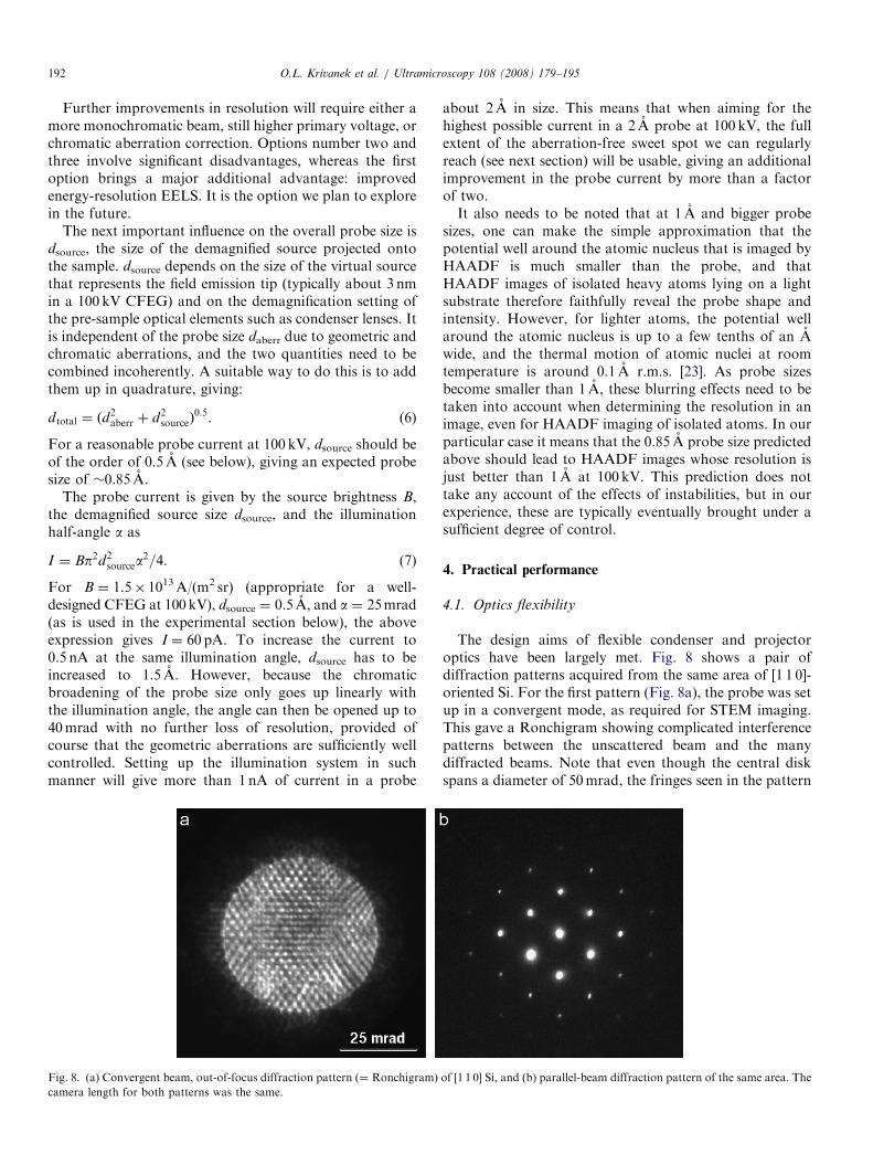
Fig. 8. (a) Convergent beam, out-of-focus diffraction pattern (¼ Ronchigram)
camera length for both patterns was the same.
about 2 A in size. This means that when aiming for thehighest possible current in a 2 A probe at 100 kV, the fullextent of the aberration-free sweet spot we can regularlyreach (see next section) will be usable, giving an additionalimprovement in the probe current by more than a factorof two.It also needs to be noted that at 1 A and bigger probe
sizes, one can make the simple approximation that thepotential well around the atomic nucleus that is imaged byHAADF is much smaller than the probe, and thatHAADF images of isolated heavy atoms lying on a lightsubstrate therefore faithfully reveal the probe shape andintensity. However, for lighter atoms, the potential wellaround the atomic nucleus is up to a few tenths of an Awide, and the thermal motion of atomic nuclei at roomtemperature is around 0.1 A r.m.s. [23]. As probe sizesbecome smaller than 1 A, these blurring effects need to betaken into account when determining the resolution in animage, even for HAADF imaging of isolated atoms. In ourparticular case it means that the 0.85 A probe size predictedabove should lead to HAADF images whose resolution isjust better than 1 A at 100 kV. This prediction does nottake any account of the effects of instabilities, but in ourexperience, these are typically eventually brought under asufficient degree of control.
4. Practical performance
4.1. Optics flexibility
The design aims of flexible condenser and projectoroptics have been largely met. Fig. 8 shows a pair ofdiffraction patterns acquired from the same area of [1 1 0]-oriented Si. For the first pattern (Fig. 8a), the probe was setup in a convergent mode, as required for STEM imaging.This gave a Ronchigram showing complicated interferencepatterns between the unscattered beam and the manydiffracted beams. Note that even though the central diskspans a diameter of 50mrad, the fringes seen in the pattern
of [1 1 0] Si, and (b) parallel-beam diffraction pattern of the same area. The

ARTICLE IN PRESSO.L. Krivanek et al. / Ultramicroscopy 108 (2008) 179–195 193
run straight. This shows that the aberrations werecorrected to a sufficient extent for aberration-free STEMimaging with a probe of this angular range.
The second pattern was recorded immediately after thefirst one, with the incident beam much more parallel,spanning an angular range of only about 0.5mrad. The OLand the projector lenses were run exactly as before, i.e. thecamera length was not changed. The probe location wasalso similar. STEM images could also be obtained in thismode, but only at a resolution of about 4 nm. This isnevertheless useful for identifying precipitates, whosestructure can then be studied using their point diffractionpatterns.
The acquisition time for the diffraction patterns,acquired by the 1k� 1k CCD, was 0.067 s each (15 framesper second). This means that each pattern was inte-grated over 3.3 cycles of AC mains. The fact that fringesrunning in all directions, including fringes corresponding to(004)-type interference (1.36 A), can be clearly distin-guished in Fig. 8a means that there were no overwhelminginstability issues, including instabilities at AC mainsfrequencies.
Because the projector column is sufficiently flexible toproduce regular CTEM images, the two probe typesdescribed above can be directly imaged on the CCDcamera. With parallel-beam illumination, phase contrastCTEM resolution was found to be as expected for a 100 kVcolumn with a Cs of 1.1mm: about 0.3 nm.
4.2. Probe size and current, HAADF and EELS resolution
Fig. 9 shows an experimental Ronchigram obtained withthe new microscope, in which the ‘‘sweet spot’’ (the part ofthe aperture plane that is not affected by geometric
Fig. 9. An experimental Ronchigram obtained with the C3/C5 corrector
that is a part of the present column, demonstrating correction up to
40mrad half-angle. The best sweet spot theoretically obtainable with the
new corrector, the sweet spot obtainable with Nion’s previous (C3-only)
corrector, and the sweet spot of the microscope running with the corrector
turned off are also indicated.
aberrations) has a radius of 40mrad. The theoreticalprediction that takes into account seventh-order aberra-tions that limit the performance of the new corrector isactually 57mrad half-angle at 100 kV (see Section 3.2).However, this theoretical size does not include anycontributions from parasitic aberrations or from instabil-ities. A less optimistic sweet spot of 50mrad is alsoindicated in the figure (as a dashed circle), together withsweet spots reachable by Nion’s previous C3-only correc-tor, and by an uncorrected 100 kV STEM.Limited precision of tuning is the most likely reason why
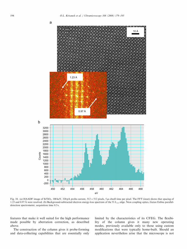
we have not reached sweet spots greater than 40mrad yet.The precision of autotuning algorithms improves asthe resolution improves, in an iterative manner. Asexplained in Section 3.2, however, chromatic aberrationprevents us from improving the resolution much past 1 A at100 kV, and this limits the precision of the tuning.At 200 kV, chromatic aberration will be less of a limit,and the precision of the tuning is expected to improvecorrespondingly.Fig. 10 shows a HAADF image and an electron energy-
loss spectrum of SrTiO3 recorded at 100 kV with the newmicroscope. The illumination half-angle was 40mr, thebeam current was 320 pA and the HAADF image(Fig. 10a) per-pixel dwell time was 5 ms. At this acquisitionspeed, the non-line-synched 512� 512 pixel image wasrecorded in 1.3 s. Even so, an FFT of the image (inset)shows that spacings of 1.23 and 0.97 A were captured.The microscope’s post-sample coupling optics collected
angles up to about 50mr half-angle into the Gatan Enfinaparallel EELS. Fig. 10b shows a background-subtractedenergy loss spectrum of the Ti L2,3 edge threshold peak,collected in 0.5 s with 0.2 eV/channel dispersion. The usual4-fold splitting is clearly resolved, and the signal-to-noiseratio is excellent for the short acquisition time used.Similar resolution images and EELS spectra have been
recorded at beam currents of up to 0.7 nA with the newmicroscope. A beam current of this magnitude gives signal-to-noise ratios in EELS data that allow elemental mappingto be carried out at dwell times of the order of a few msper-pixel, i.e. less than a minute for a 64� 64 pixelelemental map [24]. The probe diameter is 1–1.5 A evenat these currents. This set of experimental parameters islikely to lead to atomic-resolution, two-dimensionalchemical maps, first for elements with especially favorableEELS edges (e.g., first and second transition row metalsplus rare earths and actinides) and later on for virtually allelements as the technique improves further. The maps willbe accompanied by an ability to probe the bonding andelectronic structure, also with atomic resolution. Thiscombination of techniques promises to become a majorenabling tool of nanotechnology.
5. Conclusion
A new aberration-corrected STEM column has beendesigned and is now operational. It incorporates many new
ARTICLE IN PRESS
320030002800260024002200200018001600140012001000
800600400200
0-200
450 452 454 456 458 460 462 464 466 468
eV
Counts
1.23 Å
10 Å
0.97 Å
Fig. 10. (a) HAADF image of SrTiO3. 100 keV, 320 pA probe current, 512� 512 pixels, 5 ms dwell time per pixel. The FFT (inset) shows that spacing of
1.23 and 0.97 A were resolved. (b) Background-subtracted electron energy-loss spectrum of the Ti L2,3 edge. Nion coupling optics, Gatan Enfina parallel-
detection spectrometer, acquisition time 0.5 s.
O.L. Krivanek et al. / Ultramicroscopy 108 (2008) 179–195194
features that make it well suited for the high performancemade possible by aberration correction, as describedabove.
The construction of the column gives it probe-formingand data-collecting capabilities that are essentially only
limited by the characteristics of its CFEG. The flexibi-lity of the column gives it many new operatingmodes, previously available only to those using custommodifications that were typically home-built. Should anapplication nevertheless arise that the microscope is not
ARTICLE IN PRESSO.L. Krivanek et al. / Ultramicroscopy 108 (2008) 179–195 195
ready for, the modularity of the column and of theelectronics will almost certainly allow the microscopeto be reconfigured for the new mode, even after it wasbuilt.
The first two columns of the type described here havebeen recently installed in their respective laboratories(spring and autumn 2007). Similar to the way oursecond-generation correctors produced many revolution-ary results once users started working with them, we expectthe new instruments to quickly prove their abilities, and togo on to exciting new applications nobody has yet fullyimagined.
Acknowledgment
We are greatly indebted to our collaborators, especi-ally to Drs. P.E. Batson, A.L. Bleloch, and S.J. Pennycook,and to Profs. L.M. Brown, C. Colliex and J. Silcox,for giving us the opportunity and challenge to buildthe new microscope, and for their many specific inputs.Partial funding from NSF (grant number DMR-9977547)and in kind-contributions from Gatan Inc. and SandiaNational Laboratory are gratefully acknowledged. Furthersincere thanks are due to Dr. A.L. Bleloch for his helpin obtaining the results shown in Fig. 8 and to Prof.D.A. Muller and L. Fitting Kourkoutis for the resultsshown in Fig. 10.
References
[1] O. Scherzer, Optik 2 (1947) 114.
[2] P.W. Hawkes, E. Kasper, Principles of Electron Optics, vol. 2,
Academic Press, New York, 1996, pp. 857–863.
[3] J. Zach, M. Haider, Optik 99 (1995) 112.
[4] M. Haider, et al., J. Electron Microscopy 47 (1998) 395.
[5] O.L. Krivanek, N. Dellby, A.R. Lupini, Ultramicroscopy 78 (1999) 1.
[6] N. Dellby, et al., J. Electron Microscopy 50 (2001) 177.
[7] P.E. Batson, N. Dellby, O.L. Krivanek, Nature 418 (2002) 617.
[8] T. Yanaka, Proceedings of the 11th International EM Congress,
vol. 1, Japanese Society for Electron Microscopy, Kyoto, 1986,
p. 243.
[9] O.L. Krivanek, in: P.R. Buseck, J.M. Cowley, L. Eyring (Eds.), High-
Resolution Transmission Electron Microscopy, Oxford, 1988, p. 519.
[10] H.S. von Harrach, Microsc. Microstr. Microanal. 5 (1994) 153.
[11] M.A. O’Keefe, et al., Ultramicroscopy 89 (2001) 215.
[12] D.A. Muller, et al., Ultramicroscopy 106 (2006) 1033.
[13] W.D. Riecke, in: P.W. Hawkes (Ed.), Magnetic Electron Lenses,
Springer, Berlin, 1982, p. 163.
[14] O.L. Krivanek, N. Dellby, P.D. Nellist, US patent #6,770,887.
[15] O.L. Krivanek, et al., Ultramicroscopy 96 (2003) 229.
[16] N. Dellby, O.L. Krivanek, M.F. Murfitt, CPO-7 Proceedings, 2006,
p. 79, available at: /http://www.mebs.co.uk/Abstract%20Book.pdfS.[17] C.S. Own et al., Proceedings of Microscopy and Microanalysis,
Chicago 1105CD, 2006.
[18] N. Zaluzec, Microscopy Today 6 (2003) 8.
[19] R. Vincent, P.A. Midgley, Ultramicroscopy 53 (1994) 271.
[20] J.C.H. Spence, J. Taftø, J. Microscopy 130 (1983) 147.
[21] Z. Yu, P.E. Batson, J. Silcox, Ultramicroscopy 96 (2003) 275.
[22] M.F. Murfitt, N. Dellby, O.L. Krivanek, unpublished results.
[23] R.F. Loane, P. Xu, J. Silcox, Acta Cryst. A 47 (1991) 267.
[24] D.A. Muller, et al., Science, 2007, to be published.