materials analysis by aberration-corrected stem · atom-by-atom analysis by aberration-corrected...
TRANSCRIPT
Atom-by-Atom Analysis by Aberration-Corrected STEM*
Ondrej Krivanek Nion Company (www.nion.com)
in collaboration with
Tracy Lovejoy, George Corbin, Niklas Dellby, Neil Bacon, Petr Hrncirik, Matt Murfitt, Gwyn Skone and Zoltan Szilagyi, Nion Company
and
Phil Batson, Mick Brown, Ray Carpeneter, Matt Chisholm, Christian Colliex, Lena Fitting, Juan Carlos Idrobo, Vladimir Kolarik, David Muller, Julia Mundy,
Valeria Nicolosi, Steve Pennycook, Tim Pennycook, Quentin Ramasse, Kazu Suenaga, Wu Zhou, and many others
*scanning transmission electron microscopy
FCMN, 2013-03-26
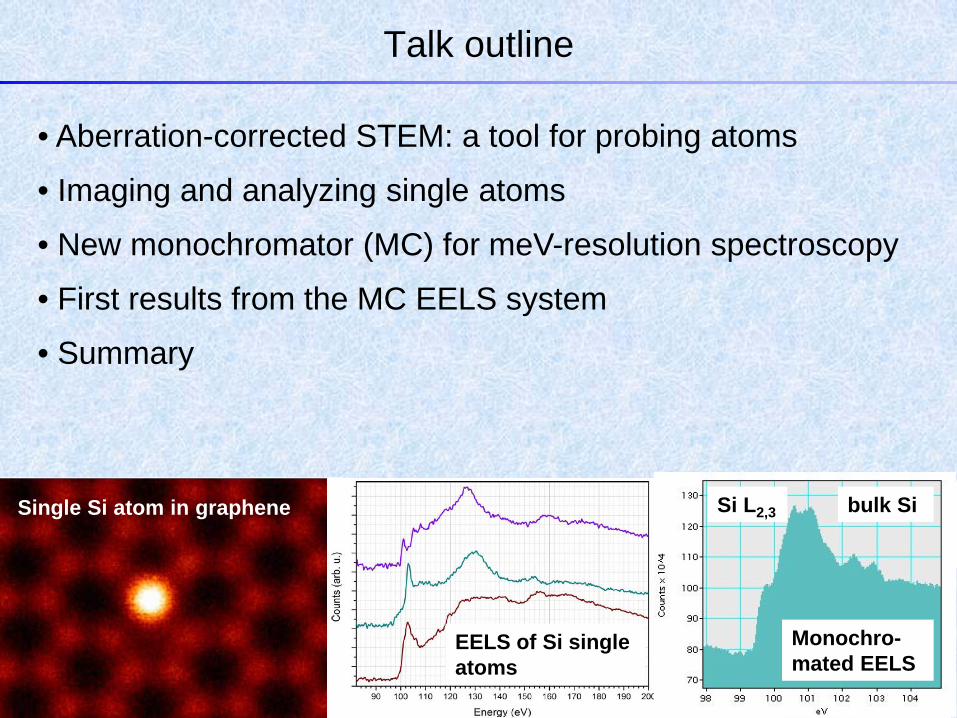
Talk outline
• Aberration-corrected STEM: a tool for probing atoms • Imaging and analyzing single atoms • New monochromator (MC) for meV-resolution spectroscopy • First results from the MC EELS system • Summary
Si in graphene
EELS of Si single atoms
Mono- chromated EELS
Single Si atom in graphene
EELS of Si single atoms
Monochro-mated EELS
Si L2,3 bulk Si
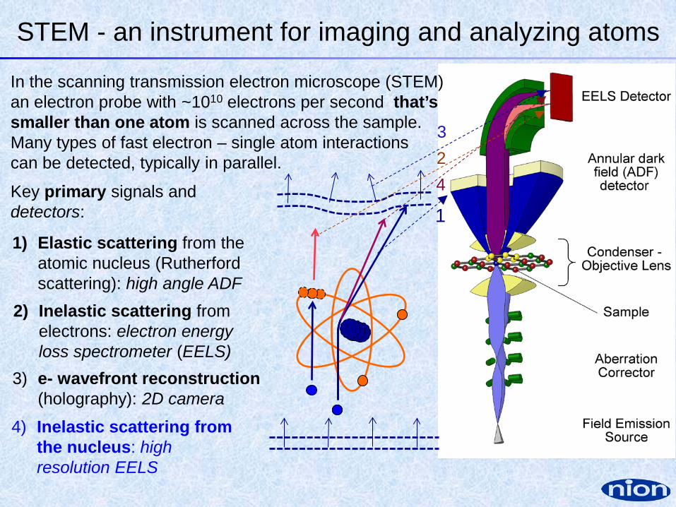
In the scanning transmission electron microscope (STEM) an electron probe with ~1010 electrons per second that’s smaller than one atom is scanned across the sample. Many types of fast electron – single atom interactions can be detected, typically in parallel.
1) Elastic scattering from the atomic nucleus (Rutherford
scattering): high angle ADF
4) Inelastic scattering from the nucleus: high resolution EELS
2) Inelastic scattering from electrons: electron energy loss spectrometer (EELS)
3) e- wavefront reconstruction (holography): 2D camera
3
STEM - an instrument for imaging and analyzing atoms
2
1 4 Key primary signals and
detectors:
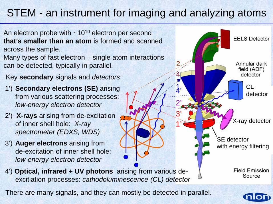
An electron probe with ~1010 electron per second that’s smaller than an atom is formed and scanned across the sample. Many types of fast electron – single atom interactions can be detected, typically in parallel.
3’) Auger electrons arising from de-excitation of inner shell hole: low-energy electron detector
STEM - an instrument for imaging and analyzing atoms
There are many signals, and they can mostly be detected in parallel.
2’) X-rays arising from de-excitation of inner shell hole: X-ray spectrometer (EDXS, WDS)
Key secondary signals and detectors: 1’) Secondary electrons (SE) arising
from various scattering processes: low-energy electron detector
4’) Optical, infrared + UV photons arising from various de-excitiation processes: cathodoluminescence (CL) detector
X-ray detector
CL detector
SE detector with energy filtering
1’
2’ 4’
3’
2
1 4
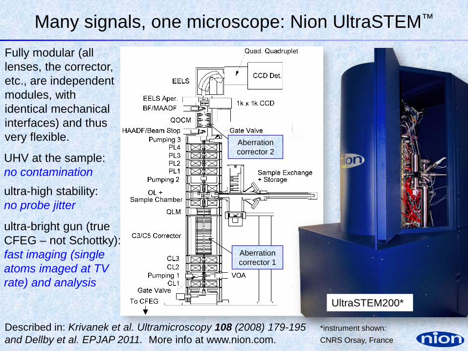
Many signals, one microscope: Nion UltraSTEM™
Aberration corrector 1
Aberration corrector 2
Described in: Krivanek et al. Ultramicroscopy 108 (2008) 179-195 and Dellby et al. EPJAP 2011. More info at www.nion.com.
UltraSTEM200*
*instrument shown: CNRS Orsay, France
Fully modular (all lenses, the corrector, etc., are independent modules, with identical mechanical interfaces) and thus very flexible.
UHV at the sample: no contamination ultra-high stability: no probe jitter
ultra-bright gun (true CFEG – not Schottky): fast imaging (single atoms imaged at TV rate) and analysis
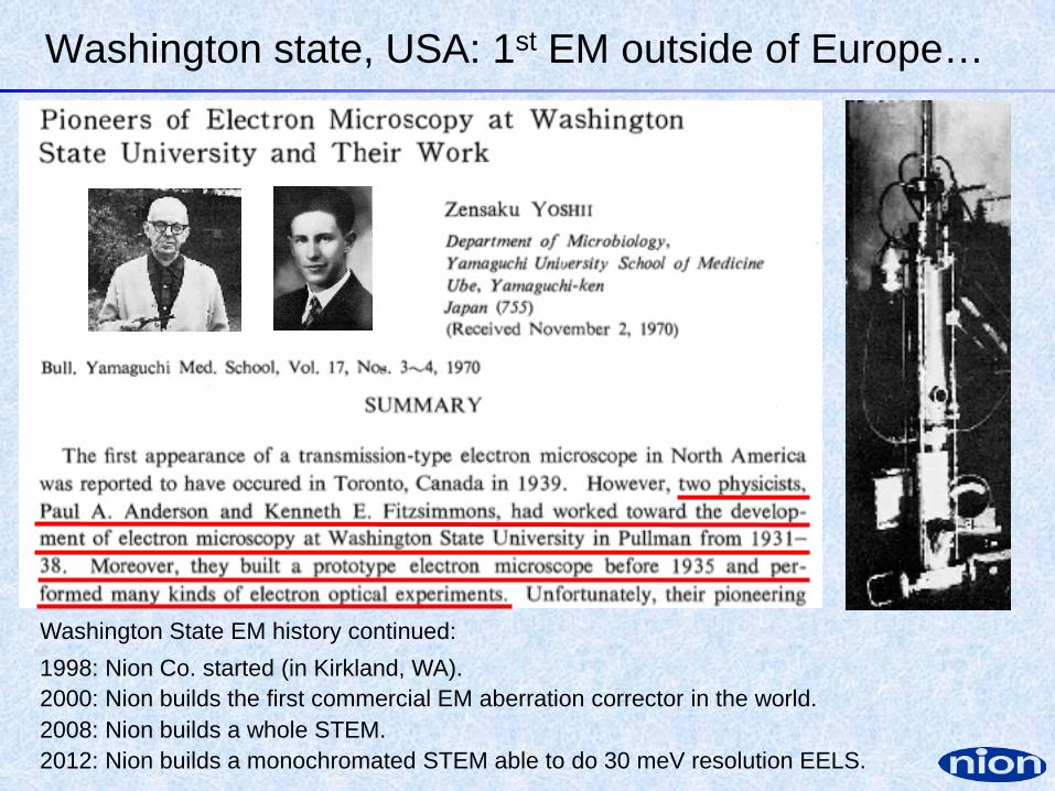
Washington state, USA: 1st EM outside of Europe…
Washington State EM history continued: 1998: Nion Co. started (in Kirkland, WA).
2008: Nion builds a whole STEM. 2000: Nion builds the first commercial EM aberration corrector in the world.
2012: Nion builds a monochromated STEM able to do 30 meV resolution EELS.
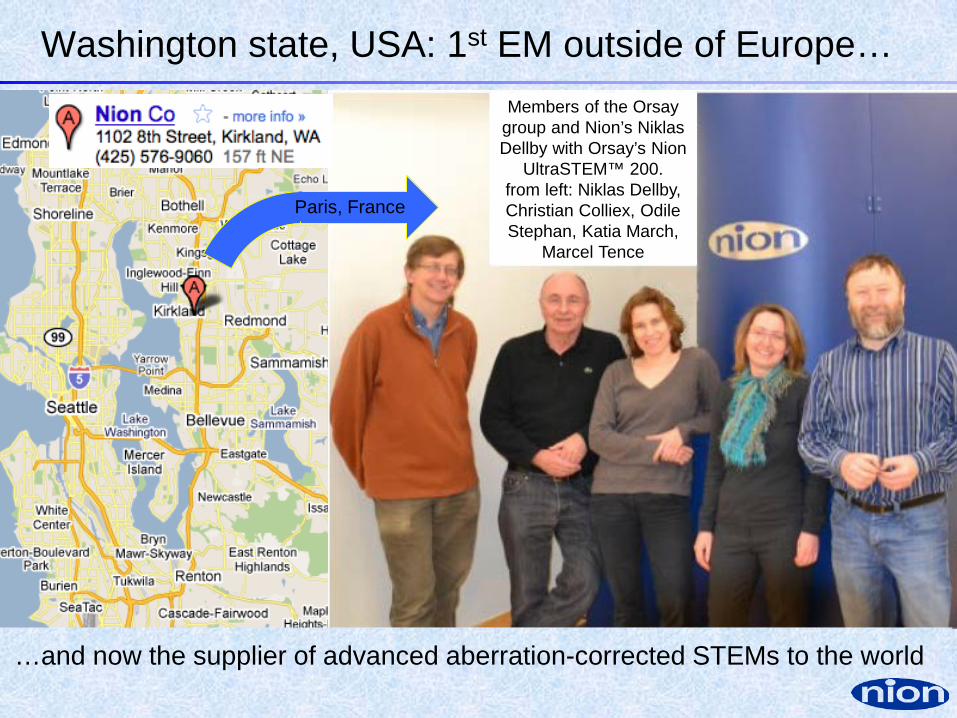
Washington state, USA: 1st EM outside of Europe…
2000: Nion (in Kirkland, WA) delivers the first commercial electron-optical aberration corrector in the world
2010: Nion delivers its first complete electron microscope (a 200 kV STEM) …and now the supplier of advanced aberration-corrected STEMs to the world
Paris, France
Members of the Orsay group and Nion’s Niklas Dellby with Orsay’s Nion
UltraSTEM™ 200. from left: Niklas Dellby, Christian Colliex, Odile Stephan, Katia March,
Marcel Tence
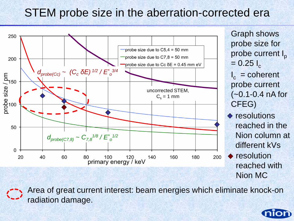
STEM probe size in the aberration-corrected era
Ic = coherent probe current (~0.1-0.4 nA for CFEG)
Graph shows probe size for probe current Ip = 0.25 Ic
uncorrected STEM, Cs = 1 mm
resolutions reached in the Nion column at different kVs
dprobe(Cc) ~ (Cc δE) 1/2 / E*o3/4
dprobe(C7,8) ~ C7,81/8 / E*
o1/2
Area of great current interest: beam energies which eliminate knock-on radiation damage.
resolution reached with Nion MC
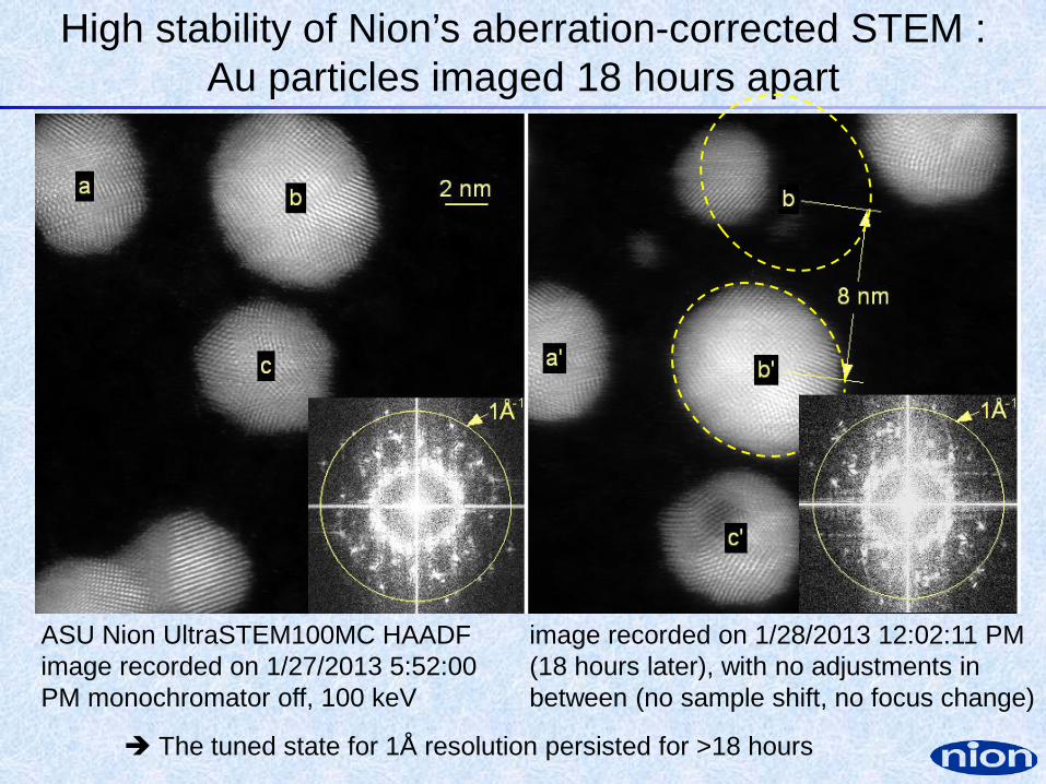
High stability of Nion’s aberration-corrected STEM : Au particles imaged 18 hours apart
ASU Nion UltraSTEM100MC HAADF image recorded on 1/27/2013 5:52:00 PM monochromator off, 100 keV
image recorded on 1/28/2013 12:02:11 PM (18 hours later), with no adjustments in between (no sample shift, no focus change)
The tuned state for 1Å resolution persisted for >18 hours
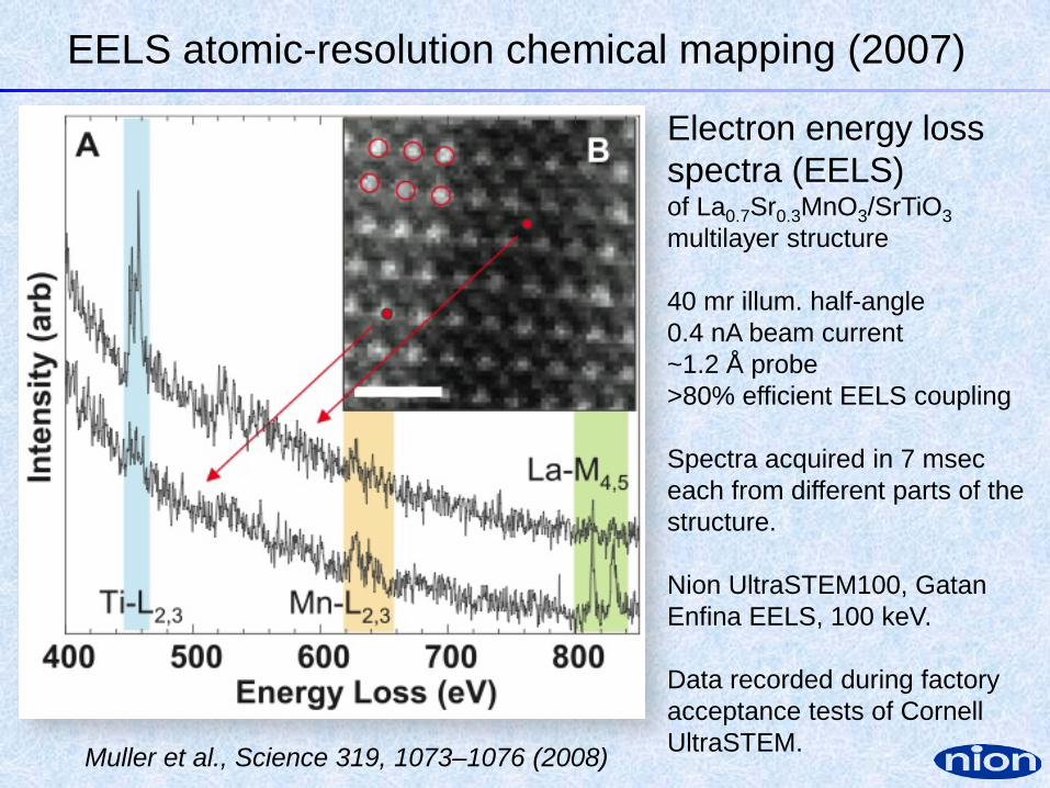
EELS atomic-resolution chemical mapping (2007)
Electron energy loss spectra (EELS) of La0.7Sr0.3MnO3/SrTiO3 multilayer structure 40 mr illum. half-angle 0.4 nA beam current ~1.2 Å probe >80% efficient EELS coupling Spectra acquired in 7 msec each from different parts of the structure. Nion UltraSTEM100, Gatan Enfina EELS, 100 keV. Data recorded during factory acceptance tests of Cornell UltraSTEM. Muller et al., Science 319, 1073–1076 (2008)
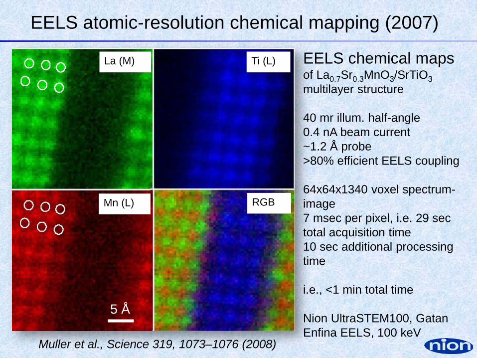
EELS atomic-resolution chemical mapping (2007)
EELS chemical maps of La0.7Sr0.3MnO3/SrTiO3 multilayer structure 40 mr illum. half-angle 0.4 nA beam current ~1.2 Å probe >80% efficient EELS coupling 64x64x1340 voxel spectrum-image 7 msec per pixel, i.e. 29 sec total acquisition time 10 sec additional processing time i.e., <1 min total time Nion UltraSTEM100, Gatan Enfina EELS, 100 keV
Muller et al., Science 319, 1073–1076 (2008)
5 Å
Mn (L)
Ti (L) La (M)
RGB
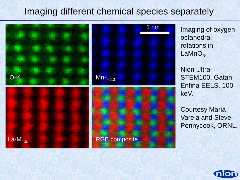
Imaging different chemical species separately
Imaging of oxygen octahedral rotations in LaMnO3. Nion Ultra-STEM100, Gatan Enfina EELS, 100 keV. Courtesy Maria Varela and Steve Pennycook, ORNL.
1 nm
O-K
La-M4,5
Mn-L2,3
RGB composite
1 nm
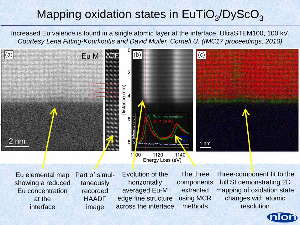
Mapping oxidation states in EuTiO3/DyScO3
Increased Eu valence is found in a single atomic layer at the interface. UltraSTEM100, 100 kV. Courtesy Lena Fitting-Kourkoutis and David Muller, Cornell U. (IMC17 proceedings, 2010)
Eu elemental map showing a reduced Eu concentration
at the interface
Part of simul-taneously recorded HAADF image
Evolution of the horizontally
averaged Eu-M edge fine structure across the interface
The three components
extracted using MCR methods
Three-component fit to the full SI demonstrating 2D
mapping of oxidation state changes with atomic
resolution
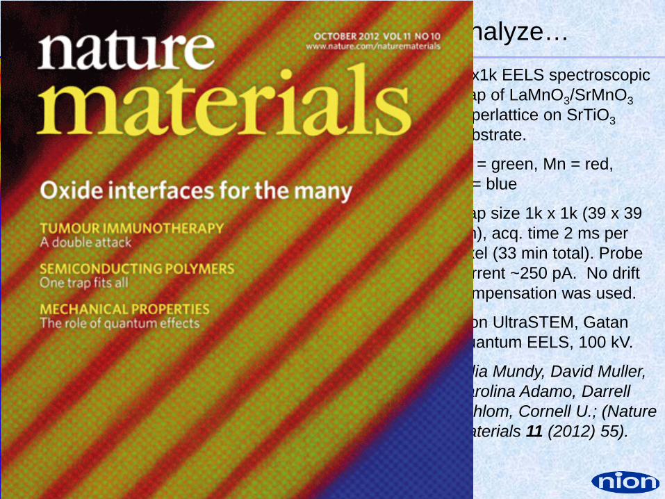
When there are more atoms to analyze…
1kx1k EELS spectroscopic map of LaMnO3/SrMnO3 superlattice on SrTiO3 substrate.
La = green, Mn = red, Ti = blue
Map size 1k x 1k (39 x 39 nm), acq. time 2 ms per pixel (33 min total). Probe current ~250 pA. No drift compensation was used.
Nion UltraSTEM, Gatan Quantum EELS, 100 kV.
Julia Mundy, David Muller, Carolina Adamo, Darrell Schlom, Cornell U.; (Nature Materials 11 (2012) 55).
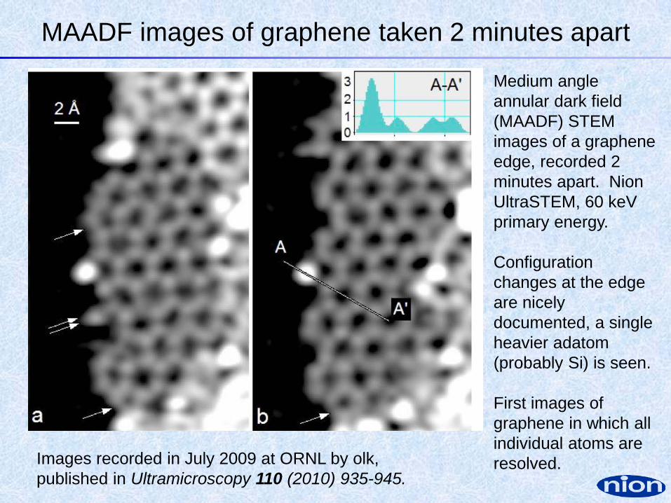
MAADF images of graphene taken 2 minutes apart
Medium angle annular dark field (MAADF) STEM images of a graphene edge, recorded 2 minutes apart. Nion UltraSTEM, 60 keV primary energy. Configuration changes at the edge are nicely documented, a single heavier adatom (probably Si) is seen. First images of graphene in which all individual atoms are resolved. Images recorded in July 2009 at ORNL by olk,
published in Ultramicroscopy 110 (2010) 935-945.
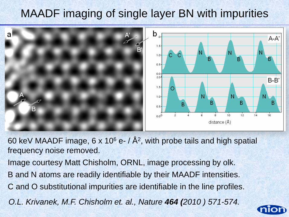
MAADF imaging of single layer BN with impurities
60 keV MAADF image, 6 x 10⁶ e- / Å2, with probe tails and high spatial frequency noise removed. Image courtesy Matt Chisholm, ORNL, image processing by olk. B and N atoms are readily identifiable by their MAADF intensities. C and O substitutional impurities are identifiable in the line profiles.
O.L. Krivanek, M.F. Chisholm et. al., Nature 464 (2010 ) 571-574.
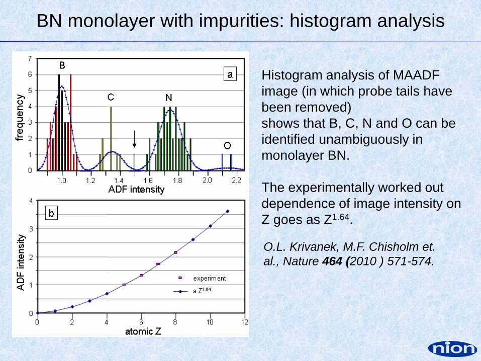
Histogram analysis of MAADF image (in which probe tails have been removed) shows that B, C, N and O can be identified unambiguously in monolayer BN. The experimentally worked out dependence of image intensity on Z goes as Z1.64.
BN monolayer with impurities: histogram analysis
O.L. Krivanek, M.F. Chisholm et. al., Nature 464 (2010 ) 571-574.
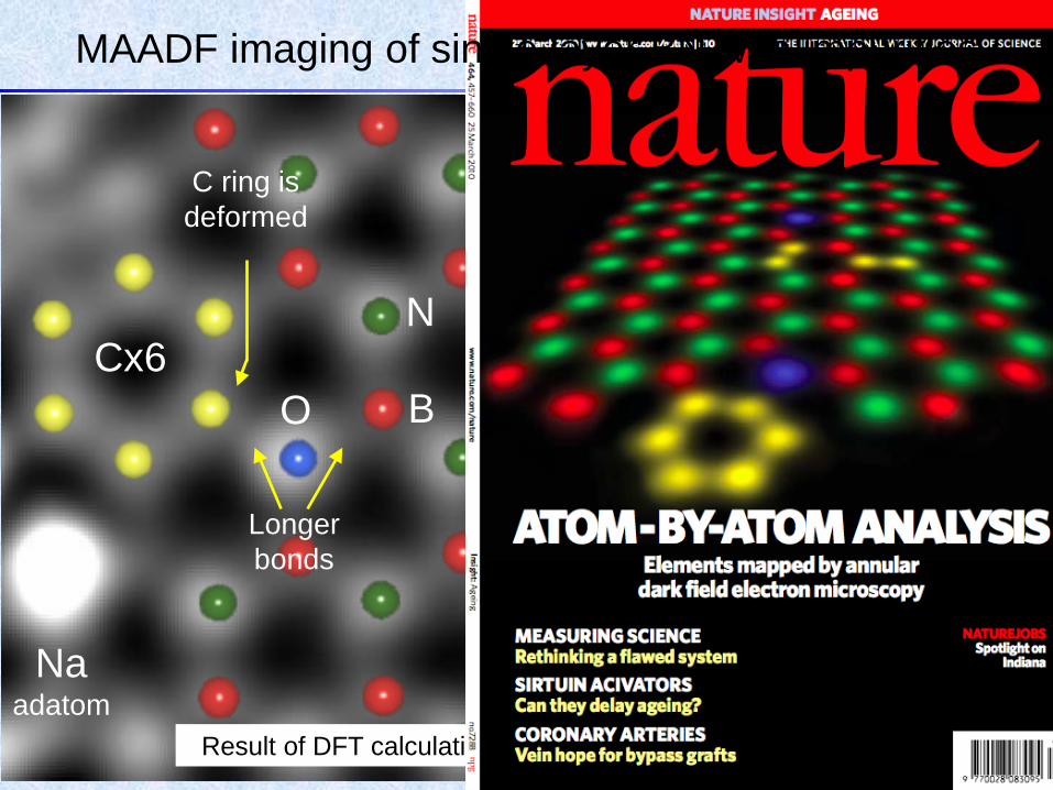
Result of DFT calculation overlaid on an experimental image
Cx6
Na adatom
O
N
Longer bonds
C ring is deformed
B C
C
O
MAADF imaging of single layer BN with impurities
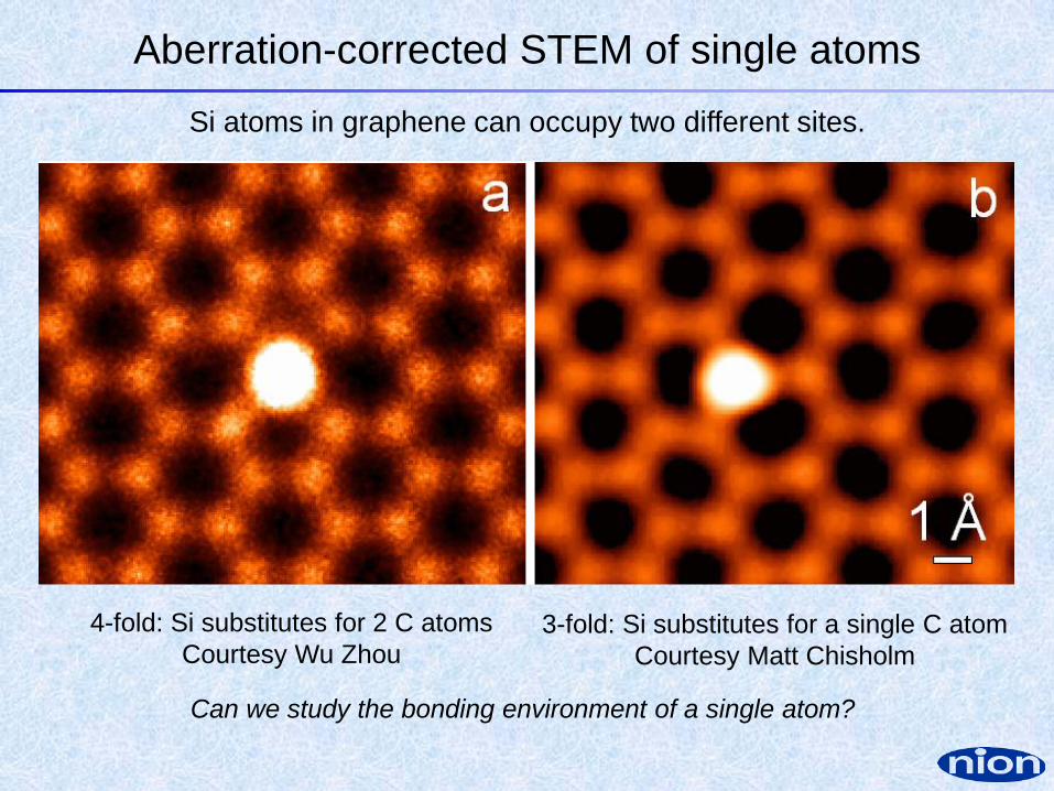
Aberration-corrected STEM of single atoms
4-fold: Si substitutes for 2 C atoms Courtesy Wu Zhou
3-fold: Si substitutes for a single C atom Courtesy Matt Chisholm
Can we study the bonding environment of a single atom?
Si atoms in graphene can occupy two different sites.
Q.M. Ramasse, C.R. Seabourne, R. Zan, D.M. Kepaptsoglou et al., Nanoletts (2013), DOI: 10.1021/nl304187e
1 nm
1 nm
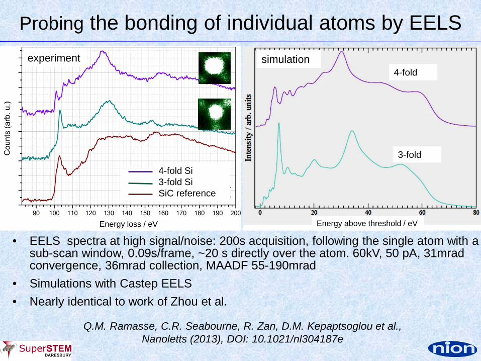
• EELS spectra at high signal/noise: 200s acquisition, following the single atom with a sub-scan window, 0.09s/frame, ~20 s directly over the atom. 60kV, 50 pA, 31mrad convergence, 36mrad collection, MAADF 55-190mrad
• Simulations with Castep EELS • Nearly identical to work of Zhou et al.
Probing the bonding of individual atoms by EELS
Energy loss / eV
4-fold Si 3-fold Si SiC reference
Energy above threshold / eV
experiment simulation 4-fold
3-fold
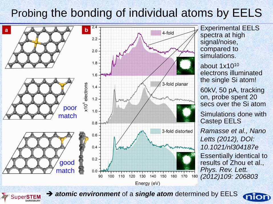
Experimental EELS spectra at high signal/noise, compared to simulations. about 1x10¹⁰ electrons illuminated the single Si atom! 60kV, 50 pA, tracking on, probe spent 20 secs over the Si atom Simulations done with Castep EELS Ramasse et al., Nano Letts (2012), DOI: 10.1021/nl304187e Essentially identical to results of Zhou et al., Phys. Rev. Lett. (2012)109: 206803
Probing the bonding of individual atoms by EELS
atomic environment of a single atom determined by EELS
poor match
good match
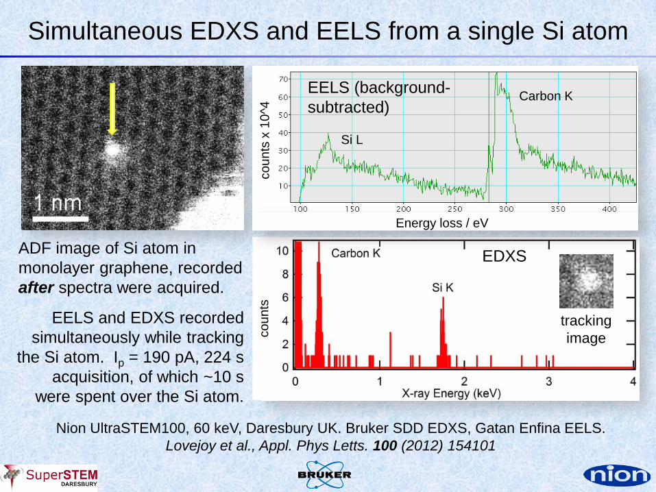
Simultaneous EDXS and EELS from a single Si atom
Nion UltraSTEM100, 60 keV, Daresbury UK. Bruker SDD EDXS, Gatan Enfina EELS. Lovejoy et al., Appl. Phys Letts. 100 (2012) 154101
ADF image of Si atom in monolayer graphene, recorded after spectra were acquired.
EELS and EDXS recorded simultaneously while tracking
the Si atom. Ip = 190 pA, 224 s acquisition, of which ~10 s
were spent over the Si atom.
tracking image co
unts
EDXS
coun
ts x
10^
4
Energy loss / eV
EELS (background-subtracted)
Si L
Carbon K
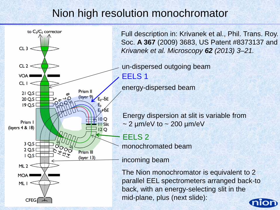
Nion high resolution monochromator
Full description in: Krivanek et al., Phil. Trans. Roy. Soc. A 367 (2009) 3683, US Patent #8373137 and Krivanek et al. Microscopy 62 (2013) 3–21.
incoming beam
energy-dispersed beam
monochromated beam
un-dispersed outgoing beam
Energy dispersion at slit is variable from ~ 2 µm/eV to ~ 200 µm/eV
EELS 1
EELS 2
The Nion monochromator is equivalent to 2 parallel EEL spectrometers arranged back-to back, with an energy-selecting slit in the mid-plane, plus (next slide):
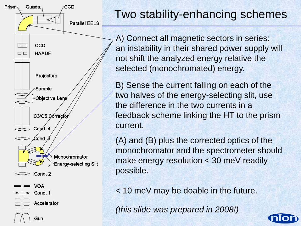
Two stability-enhancing schemes
A) Connect all magnetic sectors in series: an instability in their shared power supply will not shift the analyzed energy relative the selected (monochromated) energy.
(A) and (B) plus the corrected optics of the monochromator and the spectrometer should make energy resolution < 30 meV readily possible. < 10 meV may be doable in the future.
B) Sense the current falling on each of the two halves of the energy-selecting slit, use the difference in the two currents in a feedback scheme linking the HT to the prism current.
(this slide was prepared in 2008!)
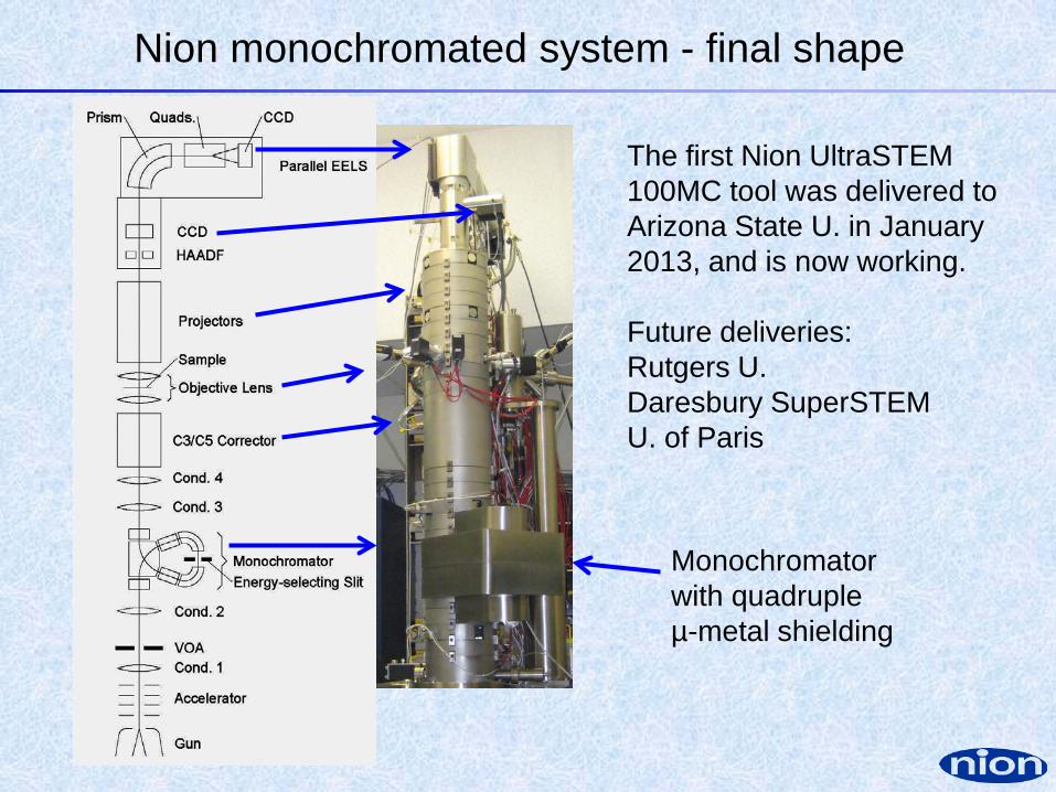
Nion monochromated system - final shape
The first Nion UltraSTEM 100MC tool was delivered to Arizona State U. in January 2013, and is now working. Future deliveries: Rutgers U. Daresbury SuperSTEM U. of Paris
Monochromator with quadruple µ-metal shielding
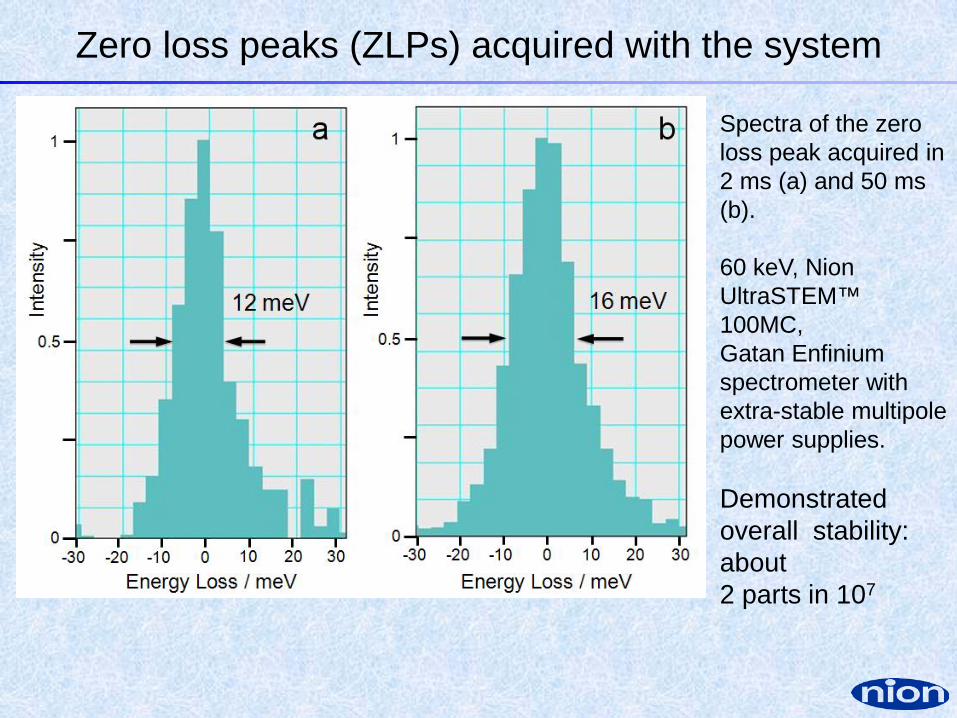
Zero loss peaks (ZLPs) acquired with the system
Spectra of the zero loss peak acquired in 2 ms (a) and 50 ms (b). 60 keV, Nion UltraSTEM™ 100MC, Gatan Enfinium spectrometer with extra-stable multipole power supplies. Demonstrated overall stability: about 2 parts in 107
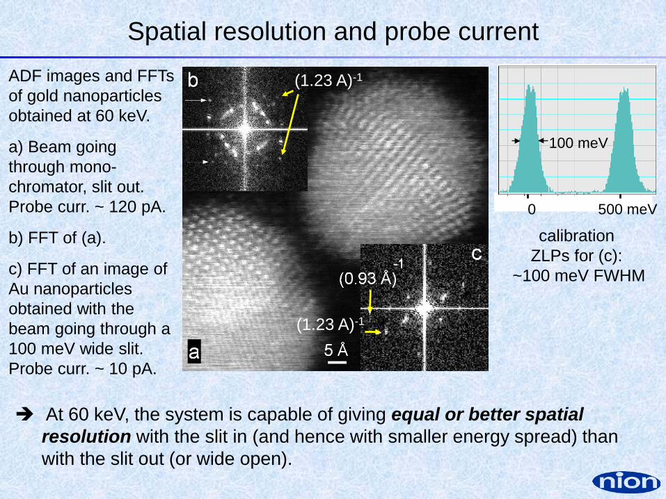
Spatial resolution and probe current
At 60 keV, the system is capable of giving equal or better spatial resolution with the slit in (and hence with smaller energy spread) than with the slit out (or wide open).
ADF images and FFTs of gold nanoparticles obtained at 60 keV.
a) Beam going through mono-chromator, slit out. Probe curr. ~ 120 pA.
b) FFT of (a).
c) FFT of an image of Au nanoparticles obtained with the beam going through a 100 meV wide slit. Probe curr. ~ 10 pA.
calibration ZLPs for (c):
~100 meV FWHM
100 meV
0 500 meV
(0.93 Å)-1
(1.23 A)-1
(1.23 A)-1

Spectra from a practical sample: SiO2 in a MOSFET (0.93 Å)-1 (1.23 A)-1
60 keV, Gatan Enfinium EELS, coupling efficiency ~100% FWHM of ZLP ~ 40 meV, ZLP height = 302. The arrowed feature in (a) is probably a band edge exciton, the arrowed features in (b) correspond to resolved L3-L2 Si L-edge spin-orbit splitting.
(acquisition time = 0.2 s) (acquisition time = 50 s)
L3 L2
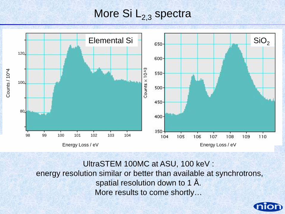
More Si L2,3 spectra
UltraSTEM 100MC at ASU, 100 keV : energy resolution similar or better than available at synchrotrons,
spatial resolution down to 1 Å. More results to come shortly…
104 105 106 107
40
50
30
Cou
nts
/ 10^
4
108 109 110 98 100 101 102 103 104 99
100
120
80
Cou
nts
/ 10^
4
Energy Loss / eV Energy Loss / eV
SiO2 Elemental Si
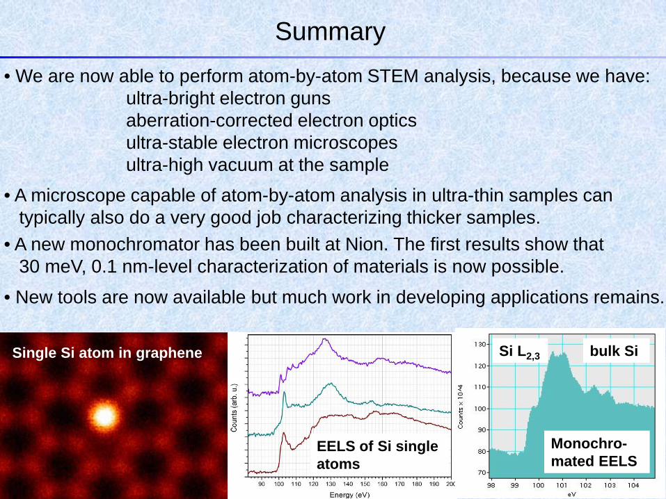
Summary • We are now able to perform atom-by-atom STEM analysis, because we have: ultra-bright electron guns aberration-corrected electron optics ultra-stable electron microscopes ultra-high vacuum at the sample
• A new monochromator has been built at Nion. The first results show that 30 meV, 0.1 nm-level characterization of materials is now possible. • New tools are now available but much work in developing applications remains.
Single Si atom in graphene
EELS of Si single atoms
• A microscope capable of atom-by-atom analysis in ultra-thin samples can typically also do a very good job characterizing thicker samples.
Si L2,3 bulk Si
Monochro-mated EELS