an analysis of thin film germanium epitaxially deposited
TRANSCRIPT

DOCID: 3927957
@'pproved for release by NSA on 11-29-2011 , Transparency Case# 63853
UNCLASSIFIED
An Analysis of Thin Film Germanium Epitaxially Deposited onto Calcium Fluoride
BY ARNOLD L. PUNDSACK
u nclassi/ied
An. experimen.l.al investigation. of ihe formation. c:Onditicn.s of thin film Ge epitaxially deposited onto ( 111) surfaces of CaF, and the resultant physi.eal and electrical. charOCter. is presen.ted. The amorpho~ to crystalline transition. region. was found to be between. 320° and 400°C, an.cl the best single-crystal orientation was faun.cl between 550° and 575°C. Average values of the mobility, conductivity, and the hole con.cen.trotion.s are also reportai with an. explanation. of the problems en.countered in. their determination.
INTRODUCTION
The formation of single-crystal thin film Ge has been the subject oi much recent interest. Sloope and Tiller' have presented the formation conditio11B for single-crystal Ge on various substrates and have also given an analysis of the resultant character of the Ge :fihns. Little else has been reported of the physical character of Ge films and l~ has been reported of the electrical properties oi thin film Ge.
This report presents the results of an experimental investigation of the formation of thin film Ge epitaxially deposited onto CaF, and an analysis of the physical and electrical character oi the resultant Ge . films. The purpose of this report is to add more data to the important and difficult to understand subject of epitaxy so that it may aid in the. better understanding of this process.
EXPERIMENTAL
The Ge films were prepared by vacuum deposition onto heated single-crystal surfaces of CaF, . .. The CaF, substrates were freshly cleaved with the (111 l face being the surface of condensation. Tbirty ohm-cm polycrystalline Ge was the source material and was resistance heated in a carbon crucible to evaporation temperatures. The deposition rate was held constant throughout the experiment and· was established by controlling the current through the crucible and measuring the resultant thickness using the Fizeau multiple-beam interference technique. The deposition l'ate of 1000A per min could be reproduced with a maximum error of 103. The substance was heated by being supported in the center of a Joule heated Al,O, cylinder, and the
23 UNCLASSIFIED

DOCID· 3927957
UNCLASSIFIED THIN FILM GERMANIUM
substrate temperature was then determined with a chromel-alumel thermocouple touching the back of the substrate.
The films were analyzed using electron transmission diffraction, electron reflection diffraction, electron microscopy, x-ray diffraction, and optical microscopy.
All of the films were prepared by heating the substrate to the desired temperature, Ge was deposited at the desired rate, and the film was cooled to room temperature before removal from the vacuum system. Two films were prepared simultaneously; one was deposited through a mask for use on the electrical measurements, and the other was used for the analysis of the structural proJ:>erties. Samples for electron tra:llsmission analysis were obtained by using a 35% solution of HCI to remove the film from the substrate. The films were all prepared in a vacuum of 1to8 X 10- 0 Torr at a source-to-substrated istance of 13 cm and a_ deposition rate of lOOOA per min.
RESULTS
The effec::t of varying the substrate temperature can be seen in Fig. 1 and Fig. 2. In Fig. 1 electron transmission diffraction patterns are shown with substrate temperature varying from 20° to 700°C, and Fig. 2 shoWll the corresponding electron micrographs for the same substrate temperatures. None of the films formed below 320°C were crystalline, and all of the films changed from amorphous to crystalline in the 320° to 400°C region. Single crystal films were produced between 500° and 600°C and, in particular, the best single-crystal films were produced at subtstrate temperatures of 550° to 575°C. It is interesting that the use of 99.99% purity Ge as the source gives approximately the same amorphous to crystalline transition region as that reported by Sloope and Tiller', using 99.99% purity Ge, and that reported by Dunoyer' as determined from electrical conductance. The temperature region reported herein for best single-crystal orientation is in close agreement with the values reported by Marucchi and Nifontoff3 and those reported by Via and Thun' for epitaxial deposition onto heated surfaces of CaF,. Fig. 2 also shows the rapid change in the microstructure at temperatures above 400°C as previously reported by Sloope and Tiller'.
While the crystalline structure and microstructure showed some definable order, the electrical properties of these thin films of Ge did not exhibit such a property. The conductivity measurements showed the maximum deviation to have occurred with Ge filffis formed at identical conditions and of the same thickness, varying up to 303 in conductivities. This phenomenon is probably due to the cleavage steps on the substrate and the irregularities present in the film. It
UNCLASSIFIED 24
----------··---------...,.--------
A. L. PUNDSACK UNCLASSIFIED
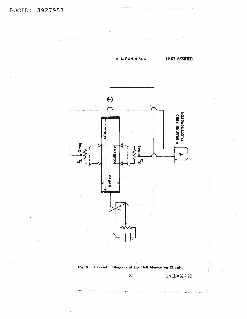
was also found that, by moving the probes close together, varying values of conductivity could be computed for the same specimen with conductivity approaching a maximum value of 30 per ohm-cm. This is probably explained by the inclusion of irregularities (more or less) in the measurement. Room temperature measurements of conductivity with a fixed probe spacing of 0.25 cm gave average values of conductivity between 10 and 15 per ohm-cm. The Hall coefficient, on the other hand, did.not exhibit this radical deviation. Figure 3 shows schematically the circuit used in determining the Hall coefficient. All of the Ge films exhibited a transverse voltage without an applied field. This transverse voltage was several orders of magnitude greater than the Hall voltage, and thus it was necessary to use the variable resistors RA and R8 to achieve null conditions without an applied magnetic field. The Hall coefficient (RH) was computed from the following relationship:
RH = VHt X 10'// H cm• per coulomb
where V H is the HALL voltage, t is the thickness in Angstroms, I is the current in amperes, and His the magnetic field in gauss. Other relationships used in determining the electrical properties of the Ge films are as follows: hole concentration (P,) equals 3.-/BeRH ; holes per cm', and hole mobility (µp) equals BRHa/3"' cm' per volt-sec.
The average values of these electrical properties as determined from the use of the above relationships were: Hall coefficients of6to12 cm' per coulomb, hole concentrations of 6 X 10 17 to 1oi• holes per cm', and hole mobilities of 50 to 150 cm' per volt-sec. It should be pointed out that these values are to be considered only approximate values because the scattering factor (3,,/8) assumes weak magnetic fields and scattering due only to lattice vibrations. Lattice vibrations are not necessarily the only type of scattering present in thin films of Ge, and there may be inhomogeneities present in the film. In the determination of the electrical properties, the maximum current used was !Oma and the maximum applied magnetic field used was six kilogauss. AU of the films were p-type and were ohmic in nature up to currents of lOma. It is interesting to note that the use of polycrystalline Ge as the source in this case should give the same conductivity type as that reported using intrinsic Ge as the source.
While wide variations were fowid in the measurement of the conductivity of films formed under identical conditions, in general the Hall coefficient seemed to increase with increasing thickness. Also when a particular probe spacing was selected, a maximum of 33 change in the conductivity was noticed over the period of !1 month.
25 UNCLASSIFIED

DOCID: 3927957
~:
UNCLASSIFIED THIN FILM GERMANIUM
DISCUSSION
Several authors have presented the formation conditions for attaining single-crystal Ge films, and the technique is rather straightforward. To have a film with specific properties is more difficult. In particular, to predict· with any reasona.ble. degree of accuracy the electrical properties from the formation conditiollB is impossible. The values of the electrical properties presented herein are to be considered only approximate values because of the nature of the beast to defy any definable order. In summary, it is hoped that the listing of average electrical properties and some of the problems encountered in their determination along with the formation conditions may aid in the better understanding of the epitaxy process.
ACKNOWLEDGEMENTS
The author is indebted to Sp/5 J. F. Cornelius for the preparation of many of the films, and to Mr. J. R. Dorsey for assistance in the analysis of the physical properties of the films.
REFERENCES
1. B. W. Sloope and C. 0. Tiller, Journal of Applied Physics, Vol. XXXIII. 1962, p. 3458.
2. J. M. Dunoyer, ibid., Vol. XI, 1956, p. 460.
3. J. Marucchi and N. Nifontoft', Comptes rendues hebdomedaires des ~ances de l' Academie de &ience, Vol. CCXLIX, 1959, p. 435.
4. G. G. Via and R. E. Thun, Traiisactions of the National Symposium on Vacuum Technology, Vol. VIII, 1962, p. 850.
UNCLASSIFIED 26
---··~---·-·

DOCID·
. ,
.
3927957
A. L. PUNDSACI<
u 0 0
. 0 '\;f"
u 0 0 N r<1
u 00
0 N
u 0
O'>
u c 0 N
UNCLASSIFIED
(.) 0 0 co (£)
0 0 C\ J 0 (!)
u 0
R II)
u 0 0 \{)
Fig. l . --Electron DJtri:action PatternN of G <) Fil.ms Deposited on CaF, with Sobst-:ra tn 'f'fJmporal,ure Va:rylng from 20° Ki 7fltP C.
27 UNCLASSIFIED
...... . . '
..... j, ' -
:
..
· ·: -:' .. . . . . .....

DOCID: 3927957
UNCLASSIHED THIN FILM. GE.HMAN fUM
<.) 0
0 0 "1"
u 0
0 (\j !"()
( ..1 0
0 0 N
u 0
(}')
u 0
0 (\j
r ' '.J I')
0 (J) ti)
0
N 0 w
Ll Q
0 I"-ff')
u <)
()
I[)
1'11{. 2. Electron Mi.cn..>gn1ph1> o f (~e l~il m!l llqx:.•bi t.et! ~m CaF, S howing t}rn Chang•J in .Microl!itruchll:'<; a ;:. it Function of the
Ku bt<tra t•o T<)rnpcrgtun-.
UNCLASSIFIED
. '~·.
··· ~ . .,
DOCID: 3927957
E u
0 q
E u
~ o ·
A. L. PUNDSACK UNCLASSIFIED
Fig. 8.- Schematic Diagram of the Hall Meaeurlng Circuit.
29 UNCLASSIFIED
... ·-· ·· - ·· .h- ~· ~··--·-· _ _ :.._ _ __ ____ .. ··- - --·- ·· ·