an 529: via optimization techniques for high … optimization techniques for high-speed channel...
TRANSCRIPT

Altera Corporation 1AN-529-1.0 Preliminary
Application Note 529
Via Optimization Techniquesfor High-Speed Channel
Designs
Introduction As more designs move toward high-speed serial links with picosecond edge rates, any impedance discontinuity in the channel can adversely affect signal quality. Channel discontinuities come from several sources and each source must be carefully considered. One commonly overlooked source of channel discontinuity is the signal via. Vias can add jitter and reduce eye openings that can cause data misinterpretation by the receiver.
This application note discusses the effects of via discontinuities in the transmission line and the ways to mitigate their effects. A time-domain reflectometer (TDR) and full-wave 3D field simulator are used to explain impedance signatures, and insertion and return losses of typical standard vias and their effect in the signal path. Also, tuning methods to make the vias more transparent to faster edge rates are evaluated. Via-tuning trade-offs are also examined because of manufacturability concerns of higher oven temperatures associated with the recent switch to restriction of hazardous substances (RoHS) processes. Finally, general guidelines and recommendations show how to design an optimized via for better high edge-rate signal transmission.
Standard Differential Via
Figure 1 shows the construction of a typical differential via in a high-speed serial link. Vias consist of the capture pads where signal traces enter or exit the vias, the drill barrel for layer transitioning, the non-functional pads (NFP or unused pads), and the via anti-pad clearance. In this via, 100-Ω differential traces enter the vias on layer 1 and exit on layer 6, while leaving a via stub from layer 6 to the bottom of the board, as well as two NFPs on layers 3 and 8, respectively.
May 2008, version 1.0

2 Altera CorporationPreliminary
Via Optimization Techniques for High-Speed Channel Designs
Figure 1. Standard Differential Via
Altera built a test board and constructed Ansoft HFSS simulation models for lab measurement to simulation correlation. This via was one of the structures included in the test board for the correlation study investigated in this application note. Figure 2 shows the layout of this via with five inches of microstrip traces serpentined on layer 1 (green) prior to entering the via and continuing along another five inches of traces serpentined on layer 6 (red). J95 through J98 are SMA connectors for the attachment of lab measurement probes from the TDR and VNA analyzers.
Figure 2. Standard Via Layout on Altera Test Board

Altera Corporation 3Preliminary
Standard Differential Via
Table 1 shows the dimensions used in the construction of this differential via. The via with this construction is referred to as a standard via. Simulation results shown in this application note compare against this standard via to show any improvement gains.
Figure 3 shows the detailed stackup of the test board. Table 2 shows the required trace geometries to meet a nominal differential impedance target of 100 Ω with ±10% tolerances. Given these design specifications, lab measurements of this standard differential via are correlated with HFSS simulation results to first calibrate the simulation setup. When calibrated, additional simulations explore and evaluate techniques for optimizing the via design.
Table 1. Standard Via Dimensions
Via Parameter Size (mils)
Drill diameter 10
Capture pad diameter 20
Anti-pad diameter 30

4 Altera CorporationPreliminary
Via Optimization Techniques for High-Speed Channel Designs
Figure 3. Test Board Stackup
Lumped pi Model
Vias can appear as capacitive and/or inductive discontinuities. These capacitive and inductive parasitics contribute to the degradation of the signal as it passes through the via. Figure 4 shows a simple lumped LC pi model to illustrate via capacitance and inductance effects. Although this
Table 2. Test Board Controlled Impedances by Layer
Impedance RequirementsFin. Line Ref Pin
2nd Ref Pin
Targeted Desired
Impedance
Impedance Tolerance
Actual Calculator Impedance
Diff Line
Centers
Diff Line
SpaceL# Impedance Type
1 SE-Coated Microstrip .00950 2 — 53.00 Ω +/- 10% 53.59 Ω — —
1 DIF-Coated Microstrip Edg .00950 2 — 100.00 Ω +/- 10% 99.55 Ω .02400 .01450
1 SE-Coated Microstrip .01075 2 — 50.00 Ω +/- 10% 50.27 Ω — —
3 SE-Stripline .00750 4 2 51.00 Ω +/- 10% 50.87 Ω — —
3 DIF-Stripline Edg Cpld .00750 4 2 100.00 Ω +/- 10% 100.10 Ω .02600 .01850
6 SE-Stripline .00700 5 7 51.00 Ω +/- 10% 50.84 Ω — —
6 DIF-Stripline Edg Cpld .00700 5 7 100.00 Ω +/- 10% 100.27 Ω .02600 .01900
8 SE-Coated Microstrip .01050 7 — 55.00 Ω +/- 10% 55.18 Ω — —
8 DIF-Coated Microstrip Edg Cpld .01050 7 — 100.00 Ω +/- 10% 100.69 Ω .02400 .01350
8 SE-Coated Microstrip .01250 7 — 50.00 Ω +/- 10% 50.36 Ω — —

Altera Corporation 5Preliminary
Cascaded Model
model is only applicable if the delay of the via is less than 1/10th of the signal rise time, it is still useful for understanding the capacitance and inductance effects.
Figure 4. Lumped pi Model of a Via
Equation 1 shows the empirical formula for the capacitance of the via. Equation 2 shows the empirical formula for the inductance of the via when vias are modeled as a lumped LC pi model.
(1)
(2)
εr is the relative dielectric constant, D1 is the diameter of the via pad, D2 is the diameter of the anti-pad, T is the thickness of the PCB, h is the via length, and d is the via barrel diameter.
To minimize the capacitive effects of the via in Equation 1, make the diameter of the via pad small while increasing the diameter of the anti-pad. Similarly, minimize the length of the via barrel in Equation 2 to reduce the inductance of the via.
Cascaded Model A representative equivalent circuit model for the standard via in Figure 1 on page 2 is shown in Figure 5. L1 is the microstrip trace on layer 1 entering the via and L6 is the stripline trace exiting the via on layer 6. As a signal travels through the via, each via pad it encounters contributes some capacitance, while each section of the via barrel adds inductance. In this case, Cpad1, Cpad3, Cpad6, and Cpad8 each represent the capacitive contribution from the via pads on layers 1, 3, 6, and 8, respectively. Similarly, L13, L36, and L68 model the inductive contribution from the portion of the via barrel transitioning from layer 1 to 3, layer 3 to 6, and layer 6 to 8, respectively. The series combination of L68 and Cpad8
L1 Trace L6 Trace
L14
Cpad1 Cpad6
Cvia1.41εrD1TD2 D1–--------------------------pF≈
Lvia 5.08h 1n 4hd------⎝ ⎠⎛ ⎞ 1+ nH≈

6 Altera CorporationPreliminary
Via Optimization Techniques for High-Speed Channel Designs
represent the via stub below layer 6. These capacitive, inductive, and stub parasitics contribute to the degradation of the signal as it passes through the via.
Figure 5. Cascaded Via Equivalent Circuit
Although Equations 1 and 2 cannot be directly applied to this equivalent model, the techniques to minimize the via capacitance and inductance still apply. To further understand these individual contributions, a HFSS full-wave 3D field simulator is used to evaluate the impedance and s-parameter profiles of vias with selected optimizations applied. These optimizations are a direct result for understanding the Cvia and Lvia described in Equations 1 and 2, and include the following:
■ Minimize Cvia by● Reducing capture pads● Eliminating NFPs● Increasing anti-pads
■ Minimize Lvia by● Eliminating and/or reducing stubs● Minimizing via barrel length by routing outer layers near
surface layers and applying backdrilling
The results from HFSS simulations, as well as TDR and VNA measurements taken from the Altera® test board, are discussed in:
■ “Effects of the Standard Via”■ “Via Optimization Techniques” on page 10■ “Addition of GND Return Vias” on page 13■ “Use of Via Backdrilling” on page 16■ “Reliability Trade-Offs” on page 18■ “Recommendations” on page 18■ “Via Tuning Guidelines” on page 18
Cpad6 Cpad8
L1 Trace
L6 Trace
L13
Cpad1 Cpad3
L36
L1 to L6 Via Transition Remaining Stub from L6 to L8
L68

Altera Corporation 7Preliminary
Effects of the Standard Via
Effects of the Standard Via
The following compares the simulated TDR and s-parameter profiles for the standard via in Figure 1 on page 2 for three different cases:
■ Layer 1 to layer 3 (long stub)■ Layer 1 to layer 6 (short stub)■ Layer 1 to layer 8 (no stub)
Figure 6 shows the TDR measurements for the test board layer 1 to layer 6 via discontinuity for calibration purposes. The measurement shows the odd-mode impedance of the test board discontinuity as 42.5 Ω at the via. Because the differential impedance for symmetrical lines is equal to twice the odd-mode impedance, this measurement translates to an equivalent differential impedance of 85 Ω . This is in line with the simulated result of 83 Ω for the differential impedance at the via, as shown in Figure 7 (layer 1 to layer 6 standard via). With the simulation calibrated, you can confidently explore different via optimizations through additional HFSS simulation.
Figure 6. Measured TDR for Standard Via

8 Altera CorporationPreliminary
Via Optimization Techniques for High-Speed Channel Designs
Figure 7. Simulated TDR Comparison for Standard Via
For completeness, Figures 8 and 9 compare the insertion and return losses (Sdd21 and Sdd11) for the same three via cases (long stub, short stub, and no stub) with HFSS simulation.
1 The test board measurements are not compared because these measurements would include more losses as a result of additional end-to-end loss contributions from the SMA connectors and 10 inches of trace routing. Conversely, simulated results model the isolated via by itself.

Altera Corporation 9Preliminary
Effects of the Standard Via
Figure 8. Simulated Sdd21 Comparison of Standard Via
Figure 9. Simulated Sdd11 Comparison of Standard Via

10 Altera CorporationPreliminary
Via Optimization Techniques for High-Speed Channel Designs
Figures 7 through 10 show that longer via stub lengths cause larger impedance discontinuity and present more loss to the signal path. You can eliminate the via stub by routing only microstrip traces on the top and bottom layers of the board. However, this might not be possible because of layout constraints, electromagnetic interference (EMI) related concerns, or other board design considerations with microstrip traces. Therefore, you must consider other ways to optimize the via for internal routing layers.
Via Optimization Techniques
You must minimize Cvia and Lvia parasitics to mitigate the effects of the via, as shown in Equations 1 and 2. Typically, via capture pads are already designed using the minimum diameter in order to maximize routing space. Therefore, perform the following optimizations to minimize Cvia and Lvia:
■ Eliminate NFPs■ Increase via anti-pad diameter■ Eliminate and/or reduce via stubs
Figures 10 through 12 compare the simulation results for the TDR profile, and insertion and return losses for the standard (non-optimized layer 1 to layer 6) via with the same via that has the aforementioned optimizations successively applied. In the figures:
■ “L1 to L6” indicate a layer 1 to layer 6 signal transition■ “No NFP” indicates removal of all non-functional pads■ “40AP” and “50AP” indicate increases in the via anti-pad to
40 mils/50 mils from the standard 30 mils.
Applying all of these optimizations improves the design of the via as illustrated by the simulation results.

Altera Corporation 11Preliminary
Via Optimization Techniques
Figure 10. TDR of Standard Via versus Via with Various Optimizations

12 Altera CorporationPreliminary
Via Optimization Techniques for High-Speed Channel Designs
Figure 11. Insertion Loss of Standard Via versus Various Optimizations

Altera Corporation 13Preliminary
Addition of GND Return Vias
Figure 12. Return Loss of Standard Via versus Various Optimizations
Addition of GND Return Vias
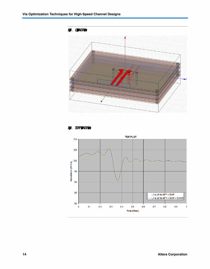
Another improvement involves providing a better AC return path by adding adjacent ground vias next to each signal via, as shown in Figures 13 through 16.
Figures 13 through 16 show the effect on the TDR, and insertion and return loss plots of adding ground vias 35 mils on either side of each signal via for the optimized 50-mil anti-pad via case. Adding ground vias provide added improvements to the impedance and insertion and return losses of the optimized via under consideration.
14 Altera CorporationPreliminary
Via Optimization Techniques for High-Speed Channel Designs
Figure 13. Optimization with GND Return Vias
Figure 14. TDR Plot with GND Return Vias

Altera Corporation 15Preliminary
Addition of GND Return Vias
Figure 15. Insertion Loss with GND Return Vias
Figure 16. Return Loss with GND Return Vias

16 Altera CorporationPreliminary
Via Optimization Techniques for High-Speed Channel Designs
Use of Via Backdrilling
For another method to optimize the via, remove the via stub by backdrilling or counter-boring the backside of the PCB with a slightly oversized drill bit to remove the parasitic stub. This method demands a cost premium over using standard vias because it requires an additional step in manufacturing the PCB. The simulated TDR and insertion and return loss plots in Figures 17 through 19 show the benefits of backdrilling by comparing a standard layer 1 to layer 3 via, versus the same via with backdrilling applied. In this case, the signal is routed from Layer 1 to Layer 3 (instead of Layer 6 as in the previous cases) to show the effect of backdrilling to remove the long stub. If shorter stubs are backdrilled, the improvements are not significant. Backdrilling can provide significant improvements, especially if the via stub is long.
Figure 17. TDR Plot of Standard L1-L3 Via versus Backdrilled L1-L3 Via

Altera Corporation 17Preliminary
Use of Via Backdrilling
Figure 18. Insertion Loss of Standard L1-L3 Via versus Backdrilled L1-L3 Via
Figure 19. Return Loss of Standard L1-L3 Via versus Backdrilled L1-L3 Via

18 Altera CorporationPreliminary
Via Optimization Techniques for High-Speed Channel Designs
Reliability Trade-Offs
With the recent transition to RoHS manufacturing processes where printed circuit boards are exposed to multiple oven cycles at a much higher temperature, removing a via’s NFPs can cause more stress on the vias as the material expands and contracts. Various studies have shown that when the via aspect ratio is high (as in the case of typical modern high-density, high-layer count PCBs), the inclusion of via NFPs can cause a reduction in long term reliability. Conversely, with low aspect ratios (larger via holes), the inclusion of NFPs can increase long-term reliability. As a result, you must be aware of and understand the reliability trade-offs that are made and tune vias according to the specific via aspect ratios used in the design.
Recommendations Because FPGA boards with transceivers tend to have high via aspect ratios (10:1 or more), Altera recommends that you optimize vias used in high-speed serial channel designs to mitigate their effect on the channel. The following summarizes guidelines that you can use to tune vias so that they are more transparent in the transmission line. Altera recommends you perform simulations to validate the design whenever possible.
Via Tuning Guidelines
Minimize Cvia by:
■ Minimizing capture pads
1 Altera’s boards regularly use 18-mil to 20-mil capture pads on 9-mil to 10-mil drill diameters, respectively.
■ Removing all non-functional pads
1 Altera recommends removing all NFPs for designs with high aspect ratio vias. Altera regularly uses 9-mil and 10-mil drills on 90-mil and 100-mil thick PCBs, respectively (an aspect ratio of 10:1).
■ Increasing anti-pad diameter
1 Altera recommends using 40-mil to 50-mil anti-pad clearances. Altera boards have achieved good performance results with 40-mil and 50-mil anti-pad via designs.
Minimize Lvia by:
■ Minimizing via stubs
1 Altera recommends using stripline routing on layers near the opposite surface of where the signal enters the via to minimize stub lengths.

Altera Corporation 19Preliminary
Conclusion
■ Adding AC return vias adjacent to each signal via:
1 Altera recommends adding ground vias placed within 35 mils center-to-center adjacent to each signal via for providing better AC return path.
■ Using backdrilling to remove stubs when appropriate.
Conclusion Vias add impedance discontinuity to the signal path. With gigabits-per-second serial channels pushing rise and fall times below 50 ps, any degradation to the transmission line can add to the problem of eye closure at the receiver. Via tuning methods discussed in this application note help minimize the impact of signal vias in the transmission line and improve channel performance.
References The following references were used in this application note:
■ Stephen W. Hall, Garrett W. Hall, James A. McCall, High-Speed Digital Systems Design, A Handbook of Interconnect Theory and Design Practices. New York, John Wiley & Sons, Inc., 2000
■ Howard Johnson and Martin Graham, High-Speed Digital Design, A Handbook of Black Magic, New Jersey, Prentice Hall, 1993
■ Bill Birch, "Discussions on Non Functional Pad Removal / Backdrilling and PCB Reliability", PWB Interconnect Solutions Inc., 103-235 Stafford Road West, Nepean, Ontario, Canada.
Document Revision History
Table 3 shows the revision history of this application note.
Table 3. Document Revision History
Date and Version Changes Made Summary of Changes
May 2008v1.0
Initial release. —