am 5-403 digital electronics wave shaping and pulse …w3jjj.com/downloads/am 5-403 digital...
TRANSCRIPT

AM 5-403
DIGITAL ELECTRONICS
WAVE SHAPING
AND
PULSE CIRCUITS
September 2012
DISTRIBUTION RESTRICTION: Approved for public release. Distribution is unlimited.
DEPARTMENT OF THE ARMY MILITARY AUXILIARY RADIO SYSTEM
FORT HUACHUCA ARIZONA 85613-7070

AM 5 – 403 Digital Electronics – Wave Shaping and Pulse Circuits
Ver 0 ii
This Page Intentionally Left Blank

AM 5 – 403 Digital Electronics – Wave Shaping and Pulse Circuits
Ver 0 i
CHANGE PAGE
LIST OF EFFECTIVE PAGES INSERT LATEST CHANGED PAGES. DISTROY SUPERSEDED PAGES
NOTE The portion of this text affected by the changes is indicated by a vertical line in the outer margins of the page. Changes to illustrations are indicated by shaded or screened areas or by miniature pointing hands.
Changes of issue for original and changed pages are: ORIGIONAL………..0…………………. Page
NO.
Change No.
Page
NO.
Change No.
Page
No.
Change No.
Title – ………………………………………….0
1-1 – 3-3 ………………………………… .0
*Zero in this column indicates an original page
A Change 0 US Army
2. RETAIN THIS NOTICE AND INSERT BEFORE TABLE OF CONTENTS. 3. Holders of this document will verify that page changes and additions indicated above have been entered. This notice page will be retained as a check sheet. This issuance, together with appended pages, is a separate publication. Each notice is to be retained by the stocking points until the standard is completely revised of canceled


AM 5 – 403 Digital Electronics – Wave Shaping and Pulse Circuits
Ver 0 i
CONTENTS
1 WAVE SHAPING ..................................................................................... 1-1
1.1 THE DIFFERENTIATION NETWORK: ......................................................................... 1-1 1.2 INTEGRATOR CIRCUIT: ..................................................................................... 1-2
1.2.1 Basic Intergrator: ................................................................................. 1-2 1.2.2 Television Vertical Intergrator: ................................................................. 1-3
1.3 SCHMITT TRIGGER ..................................................................................... 1-4
2 CLAMPING AND LIMITING: ........................................................................ 2-1
2.1 INTRODUCTION: ........................................................................................... 2-1 2.2 CLAMPERS: ................................................................................................ 2-2
2.2.1 Introduction: ...................................................................................... 2-2 2.2.2 Positive Clampers: ................................................................................ 2-2 2.2.3 Negative Diode Clamper: ........................................................................ 2-3
2.3 LIMITERS: ................................................................................................. 2-4 2.3.1 Introduction: ...................................................................................... 2-4 2.3.2 Series Limiter: .................................................................................... 2-4 2.3.3 Netagive Series Limiter: ......................................................................... 2-4 2.3.4 Shunt Limiter: ..................................................................................... 2-6 2.3.5 Positive Negative Limiter: ....................................................................... 2-6 2.3.6 Zener Limiter: ..................................................................................... 2-7
3 PULSE GENERATORS ............................................................................... 3-1
3.1 SQUARE WAVE GENERATOR USING A COMPARATOR: ........................................................ 3-1 3.2 CRYSTAL CONTROLED CMOS SQUAREWAVE GENERATOR: ................................................... 3-2 3.3 SPECIALIZED PULSE GENERATORS: ......................................................................... 3-3

AM 5 – 403 Digital Electronics – Wave Shaping and Pulse Circuits
Ver. 0 ii
PREFACE Improvements Suggested corrections, or changes to this document, should be submitted through your State Director to the Regional Director. Any Changes will be made by the National documentation team.
Distribution Distribution is unlimited.
Versions The Versions are designated in the footer of each page if no version number is designated the version is considered to be 1.0 or the original issue. Documents may have pages with different versions designated; if so verify the versions on the “Change Page” at the beginning of each document.
REFERENCES
Allied Communications Publications (ACP):
1. ACP - 121 - Communications Instruction, General 2. ACP - 124 - Radiotelegraph Procedures 3. ACP - 125 - Radiotelephone Procedures 4. ACP - 126 - Communications Instructions – Radio Teletypewriter 5. ACP - 131 - Communications Instructions Operating Signals
DOD Instructions
1. DOD Instruction 4650.2.
US Army Documents US Army Regulations
1. AR 25-6 - Military Auxiliary Radio System (MARS) and Amateur Radio Program
US Army FM/TM Manuals
1. FM 6-02.52 – Tactical Radio Operations 2. TM 5-811-3 - Electrical Design, Lightning and Static Electricity Protection
US Army MARS
1. AM 2-200 - US Army MARS Net Plan
Commercial References 1. Basic Electronics, Components, Devices and Circuits; ISBN 0-02-81860-X, By William P Hand
and Gerald Williams
Contributors This document has been produced by the Army MARS Technical Writing Team under the authority of Army MARS HQ, Ft Huachuca, AZ. The following individuals are subject matter experts who made significant contributions to this document.
William P Hand

AM 5 – 403 Digital Electronics – Wave Shaping and Pulse Circuits
Ver 0 1-1
1 WAVE SHAPING This section will present a quick review, but will show in addition how the time constant circuit can be put to good use to reshape a waveform or establish a dc reference for a signal.
1.1 THE DIFFERENTIATION NETWORK:
The differentiation network is a very simple circuit, and, with proper selection of its component values, the shape of a waveform can be altered. The circuit shown in Figure 1-1 is a differentiator, shown with its input and output waveshapes. The sudden application of the leading edge of the square wave input signal will cause maximum current to flow in R, since the capacitor has no voltage charge on it and can offer no opposition to the input voltage. The voltage drop across R will rise very rapidly to a maximum shown as point A in the figure. By selecting values of
Figure 1-1 Differentiator
Rand C, we can establish a very short time constant as compared to the input signal's period. The capacitor C will charge rapidly and the voltage drop across R, and thus the current through R, will drop in direct proportion to the charge on capacitor C, which will offer opposition to the input voltage. The capacitor will charge to full charge long before the end of the input waveform. This action is shown as point B in Figure 1-1. From point B to point C in time, no current will flow because of the charge on the capacitor. At time point C the input waveshape drops to zero volts, thus the capacitor no longer has a voltage driving it. Therefore, it will send a surge of current of the opposite polarity through R, from time point C to time point D. With a short time constant the capacitor will discharge fully in a very short period, as shown by the waveform from time point D to point E. From time point E to time point F the voltage across R will remain at zero volts because there is no input nor is there a charge on capacitor C to produce an output. Thus a complete cycle of the input signal gives two output pulses, one positive (charging) and the other negative (discharging).

AM 5 – 403 Digital Electronics – Wave Shaping and Pulse Circuits
Ver. 0 1-2
1.2 INTEGRATOR CIRCUIT:
1.2.1 BASIC INTERGRATOR:
An RC circuit may be constructed, so that the charging time is short and the discharge time is long. A circuit that has these characteristics is shown in Figure 1-2. The short time for charging permits the capacitor to charge to full input voltage long before the input signal's first half-cycle, as shown in the waveshapes of the figure. When the input signal reaches its second half-cycle time, as shown in part (A) of the figure, the capacitor will begin to discharge toward zero volts.
Figure 1-2 Basic Integrator Circuit and waveshape

AM 5 – 403 Digital Electronics – Wave Shaping and Pulse Circuits
Ver 0 1-3
1.2.2 TELEVISION VERTICAL INTERGRATOR:
A good example of this type of circuit is the television vertical integrator. A time constant on the order of about 100 microseconds is common. This time constant can be obtained as follows:
T = RC T = (1000,000)(0.001 µF) T = 100,000 X 0.000000001 T = 0.0001 seconds T = 100 microsecondes
Figure 1-3 shows a typical TV vertical sync integrator. Pulses are fed into the integrator are of various widths, as shown in the input waveshape of the figure. Note that there are also differently timed intervals between the pulses. The integrator, because of its time constant, ignores the short pulses, called equalizing pulses, and will begin to recognize the wide pulses as the pulses it is designed to see. The capacitor charges only to a very low voltage during the time the equalizing pulses are present and' will almost fully discharge between them. But when the wider vertical pulses appear, with the much shorter time between them, the capacitor will charge during the pulses and discharge very little between, thus giving a stepping increase charge to the capacitor that can be used by the television receiver to sort 60 Hz pulses out of a composite waveform that contains both 60 Hz and 15,750 Hz pulses.
Figure 1-3 Television Integrator
Integrator circuits can be used to generate a triangular waveshape. If the capacitor is allowed to charge through a high resistance, it will develop a long exponential charge curve by gradually building the charge on the capacitor over a long time period. The capacitor discharges much faster than it charges because the discharge occurs through the output load of the circuit, which is of much lower resistance than the charging resistance. This type of circuit is widely used in electronic circuits. Some oscillators such as the 4-layer diode oscillator depend upon the time constant of an R C charge-discharge time to establish their operating frequency.

AM 5 – 403 Digital Electronics – Wave Shaping and Pulse Circuits
Ver. 0 1-4
1.3 SCHMITT TRIGGER
The Schmitt trigger is another circuit designed for pulse shaping. If any waveshape, of sufficient amplitude, is applied to the input of the circuit, the output will be a rectangular waveshape (reference Figure 1-4).
Figure 1-4
Schmitt Trigger Waveshapes A Schmitt trigger circuit produces an output only when the input signal has reached desired amplitude. (reference Figure 1-5) To have an output, the input signal must overcome the circuit bias. Since the bias is adjustable, it is possible to control the amount of signal required to trigger the circuit.
Figure 1-5
Schmitt Trigger Circuit

AM 5 – 403 Digital Electronics – Wave Shaping and Pulse Circuits
Ver 0 1-5
There is an output only when the input signal input overcomes the reference level. No particular signal waveshape is required as long as the amplitude is high enough. The output is amplitude. The width of the output pulse depends upon how long the input is equal to or above the reference level. The input signal amplitude necessary to develop an output is determined by the reference level. A Schmitt trigger of discrete components is shown in Figure 1-5. In the circuit’s quiescent state, transistor Q1 is at cut-off, with the collector voltage approximately equal to - V. This negative voltage is coupled to the base of Q2 through resistor R3 and the base voltage of transistor Q2 is equal to the voltage drop across resistor Rs. Current flow from the emitter of resistor R4 keeps the emitter of QI at a negative potential. This reverse bias is developed between the emitter and the base of transistor QI maintains the cutoff condition. A sufficiently high negative voltage at the base of transistor Q2 produces forward bias for the emitter base junction and drives it into saturation. A negative signal of sufficient amplitude that is applied to the base of transistor Q1 overcomes the reverse bias and causes transistor Q1 to conduct, the potential at the collector decreases and becomes less negative. This change is coupled to the base of transistor Q2. The emitter current of transistor Q2 decreases, lowering the potential across resistor R4. The emitter of transistor Q1 becomes less negative, reducing the reverse bias and increasing collector current. This regenerative action continues until transistor Q1 is operating in the saturated region and transistor Q2 is at cutoff. The output voltage is a maximum negative voltage as shown in the output waveform in Figure 1-5. This stable condition continues until the input begins to rise to become more positive. The positive-going input decreases the base potential of transistor QI and increases the reverse bias, causing the collector voltage to increase (become more negative), the emitter current to decrease, and the potential across R4 to decrease, simultaneously.


AM 5 – 403 Digital Electronics – Wave Shaping and Pulse Circuits
Ver 0 2-1
2 CLAMPING AND LIMITING:
2.1 INTRODUCTION:
Often a DC reference level of a signal must be changed or set to a certain dc value despite input signal variations. The circuit shown in Figure 2-1 can be used to accomplish this. The circuit will not distort the input signal's waveshape if the time constant of the RC network is long compared to the time period of the input signal. The circuit's ability to pass a signal without distortion, the circuit can be used with complex input signals. The capacitor blocks incoming dc level so the signal will swing around a ground (zero) reference level. In the example (Figure 2-1) the resistor is reference to ground. This causes average dc output to be zero. The shaded area shows the positive alternation equals the negative alternation. As can be seen, the signal is not a symmetrical square wave. It has a narrower, but in higher, positive pulse as compared to the negative portion. If the input were a symmetrical square wave, the positive and negative swings would be of equal amplitude. A signal's peak value, with respect to its reference, depends upon its waveshape. Also, the peak value will vary directly with the signal strength. Although the capacitor establishes a dc reference for the output, the output, is not clamped to a specific voltage.
Figure 2-1 Basic Clamper
By employing a diode in conjunction with a capacitor and resistor, the input signal can be damped to any dc reference voltage. This clamping can be easily accomplished by biasing to the desired level.

AM 5 – 403 Digital Electronics – Wave Shaping and Pulse Circuits
Ver. 0 2-2
2.2 CLAMPERS:
2.2.1 INTRODUCTION:
A damper is a circuit that permits the voltage of a waveform to rise or fall only as far as a specific reference voltage. Clampers may have a negative or positive reference voltage.
2.2.2 POSITIVE CLAMPERS:
Positive Diode Clamper It can be seen in Figure 2-2 that the output from each circuit is clamped to a dc voltage reference. The output of the positive diode clampers are always above the reference, whatever it may be. As with the circuit of Figure 2-2, the waveshape and the peak-to-peak amplitude of the input are left unchanged by the circuit. The output end of the capacitor is kept charged above the clamping reference level by approximately the peak voltage of the input signal by the rectifying action of the diode. Because of this, the output signal rides on top of the dc clamping reference voltage. As an illustration, let us apply a symmetrical sawtooth waveshape to the input of a diode clamper with a signal dc reference of 0 volts and a peak-to-peak voltage of 8 volts. If we have a clam per bias of -2 volts, the reference for the clamper is thus -2 volts. The output signal will therefore be a symmetrical sawtooth waveshape that varies from -2 volts to +6 volts with a peak-to-peak voltage of 8 volts, identical to the input signal.
Figure 2-2
Positive Diode Clampers

AM 5 – 403 Digital Electronics – Wave Shaping and Pulse Circuits
Ver 0 2-3
2.2.3 NEGATIVE DIODE CLAMPER:
Negative Diode Clamper In the- negative diode clampers shown in Figure 2-3, the cathode of the diode in each circuit is connected to the reference rather than the anode as in the positive clam per. With the diode thus connected, it will keep the capacitor charged below the clamping reference by an amount equal to the peak voltage of the input signal. Because of this diode action, the output rides below the reference clamp voltage in negative dampers.
Figure 2-3
Negative Diode Clampers A quick method for identifying the type of clamper (positive or negative) is to note the arrow direction on the diode. If it points toward the bias or ground, the clam per is a negative clam per. Check the circuits of Figures 2-3 and 4-4 to verify this.

AM 5 – 403 Digital Electronics – Wave Shaping and Pulse Circuits
Ver. 0 2-4
2.3 LIMITERS:
2.3.1 INTRODUCTION:
A circuit that limits the amplitude of either the positive or negative excursion or both is known as a limiter, (sometimes called a clipper), because it limits or clips the positive peak, negative peak, or both of the input signal. This clipping or limiting will flatten the peaks of the input waveshape in doing its job. Limiters are used extensively in pulse waveshaping. A sine wave can be limited or clipped to almost a square wave. The output of oscillators can be improved and distorted pulse shapes can be corrected. A limiter can also be used to prevent unwanted amplitude variations and to help eliminate system
2.3.2 SERIES LIMITER:
Series Limiter A series limiter is formed by placing a diode in series with the load. The circuit also has a resistor to a bias voltage or to ground as needed. For this version of the circuit, the diode is reverse-biased by the input signal. The limiting is, of course, not perfect because of the reverse current flow. To get the best limiting action, it is necessary to make the resistor as small as possible compared to the reverse resistance of the diode. The circuit shown in Figure 2-4 is called a positive limiter, because it will limit the upward swing of the input signal. The basic circuit is unbiased and will therefore limit at 0 volts. It is a simple half-wave rectifier, with only the negative alternation appearing across the resistor. By utilizing a positive bias, only part of the positive alternation is clipped. The clipping reference in Figure 2-5 is +E and the diode conducts until the input signal reaches this +E voltage. When the input signal reaches the +E voltage value, it reverse bias the diode, which then becomes a very high resistance. This high resistance virtually blocks the input, thus giving an output of +E as long as the amplitude of the input exceeds the +E bias level.
2.3.3 NETAGIVE SERIES LIMITER:
Negative Series Limiter to get a negative series limiter, all we have to do is to reverse the diodes in the circuit just discussed. A negative series limiter is shown in Figure 2-5. By reversing the diodes, we get the opposite type of clipping as the rectification action occurs in the opposite direction from the positive limiter. In Figure 2-6 a polarity opposite to that of Figure 2-4 is shown. The negative alternation is clipped. If less clipping is desired, a negative bias is applied. If more is wanted, a positive bias is applied.

AM 5 – 403 Digital Electronics – Wave Shaping and Pulse Circuits
Ver 0 2-5
Figure 2-4
Positive Series Limiter
Figure2-5
Negative Series Limiter
AM 5 – 403 Digital Electronics – Wave Shaping and Pulse Circuits
Ver. 0 2-6
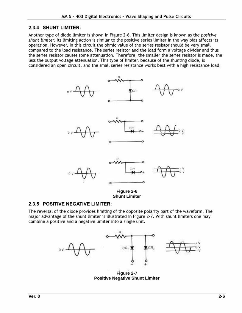
2.3.4 SHUNT LIMITER:
Another type of diode limiter is shown in Figure 2-6. This limiter design is known as the positive shunt limiter. Its limiting action is similar to the positive series limiter in the way bias affects its operation. However, in this circuit the ohmic value of the series resistor should be very small compared to the load resistance. The series resistor and the load form a voltage divider and thus the series resistor causes some attenuation. Therefore, the smaller the series resistor is made, the less the output voltage attenuation. This type of limiter, because of the shunting diode, is considered an open circuit, and the small series resistance works best with a high resistance load.
Figure 2-6
Shunt Limiter
2.3.5 POSITIVE NEGATIVE LIMITER:
The reversal of the diode provides limiting of the opposite polarity part of the waveform. The major advantage of the shunt limiter is illustrated in Figure 2-7. With shunt limiters one may combine a positive and a negative limiter into a single unit.
Figure 2-7
Positive Negative Shunt Limiter

AM 5 – 403 Digital Electronics – Wave Shaping and Pulse Circuits
Ver 0 2-7
2.3.6 ZENER LIMITER:
As you will recall, a zener diode is a diode that operates in its break down region. As shown in Figure 2-8, b: selection of the zeners operation voltage the clipping point can be selected without a bias supply. Also as shown, a positive/ negative, clipper / limiter can be made with a single symmetrical Zener diode.
Figure 2-8
Zener Diode Limiter


AM 5 – 403 Digital Electronics – Wave Shaping and Pulse Circuits
Ver 0 3-1
3 PULSE GENERATORS
3.1 SQUARE WAVE GENERATOR USING A COMPARATOR:
An inexpensive and fairly stable square wave generator can be designed around an op amp, or comparator. The circuit of Figure 3-1 employs an RC feedback network to the inverting input and resistive feedback to the noninverting input of an op amp. The threshold for switching is defined by the ratio of Rl to the sum of R1 and Rz . The timing capacitor C charges to the positive threshold when the output is of the circuit at +V. When this positive threshold is reached, the output switches to - V and the capacitor begins charging from the positive threshold back to the negative threshold. If Rl = O.86RZ, the frequency of oscillation, f, is:
If Rl =t= O.86RZ, then the frequency of oscillations becomes:
Figure 3-1 A Comparator Square Wave Generator

AM 5 – 403 Digital Electronics – Wave Shaping and Pulse Circuits
Ver. 0 3-2
3.2 CRYSTAL CONTROLED CMOS SQUAREWAVE GENERATOR:
Figure 3-2 shows a CMOS inverter package and an inexpensive quartz crystal that will generate a reliable and stable rectangular waveform. The operating frequency, f, is primarily determined by the crystal and can range from 10 kHz to as high as 1 MHz. The power supply voltage can fall anywhere within the normal operating range of CMOS inverters. The actual component values are relatively non-critical, but can be trimmed for optimum performance with a particular crystal and a given circuit board layout.
The basic design equations for the circuit are:
R1 = 5 x 10⁶e-(10 x 10-6f) R2 = 0.12R1 R3 = R2/(0.3Vcc - 0.5)
Figure 3-2
A Comparator Square Wave Generator

AM 5 – 403 Digital Electronics – Wave Shaping and Pulse Circuits
Ver 0 3-3
3.3 SPECIALIZED PULSE GENERATORS:
There are certain applications, such as testing. in analog systems, where it is necessary to generate nonstandard periodic waveform. Figure 3-3 is a block diagram of a circuit that can generate nearly any desired waveform. The practicality of the circuit depends primarily upon frequency and resolution. The D/A converter can range from a simple R-2R ladder to a high-accuracy monolithic converter. The n-bit counter can vary from 2 to N bits, depending on the desired resolution of the output desired. Likewise, the ROM length and width are determined by the desired horizontal and vertical resolutions, respectively.
Figure 3-3 Arbitrary Waveform Generator
The key design equations for this circuit are:
fin = 2NfO
where N is the number of bits in the counter, fin is the clock frequency, and fO is the desired output
frequency.
Vertical (amplitude) resolution = 1 part in 2w where W is the ROM width.
Horizontal (time) resolution = 1 part in 2L where L is the ROM length.