alternative solder bond packaging approach for high ... · alternative solder bond packaging...
TRANSCRIPT

ARL-TR-7830 ● SEP 2016
US Army Research Laboratory
Alternative Solder Bond Packaging Approach for High-Voltage (HV) Pulsed Power Devices
by Aderinto Ogunniyi, Gail Koebke, Heather O'Brien, and Oladimeji Ibitayo Approved for public release; distribution unlimited.

NOTICES
Disclaimers
The findings in this report are not to be construed as an official Department of the Army position unless so designated by other authorized documents.
Citation of manufacturer’s or trade names does not constitute an official endorsement or approval of the use thereof.
Destroy this report when it is no longer needed. Do not return it to the originator.

ARL-TR-7830 ● SEP 2016
US Army Research Laboratory
Alternative Solder Bond Packaging Approach for High-Voltage (HV) Pulsed Power Devices
by Aderinto Ogunniyi, Gail Koebke, Heather O’Brien, and Oladimeji Ibitayo Sensors and Electron Devices Directorate, ARL Approved for public release; distribution unlimited.

ii
REPORT DOCUMENTATION PAGE Form Approved OMB No. 0704-0188
Public reporting burden for this collection of information is estimated to average 1 hour per response, including the time for reviewing instructions, searching existing data sources, gathering and maintaining the data needed, and completing and reviewing the collection information. Send comments regarding this burden estimate or any other aspect of this collection of information, including suggestions for reducing the burden, to Department of Defense, Washington Headquarters Services, Directorate for Information Operations and Reports (0704-0188), 1215 Jefferson Davis Highway, Suite 1204, Arlington, VA 22202-4302. Respondents should be aware that notwithstanding any other provision of law, no person shall be subject to any penalty for failing to comply with a collection of information if it does not display a currently valid OMB control number. PLEASE DO NOT RETURN YOUR FORM TO THE ABOVE ADDRESS.
1. REPORT DATE (DD-MM-YYYY)
September 2016 2. REPORT TYPE
Technical Report 3. DATES COVERED (From - To)
4. TITLE AND SUBTITLE
Alternative Solder Bond Packaging Approach for High-Voltage (HV) Pulsed Power Devices
5a. CONTRACT NUMBER
5b. GRANT NUMBER
5c. PROGRAM ELEMENT NUMBER
6. AUTHOR(S)
Aderinto Ogunniyi, Gail Koebke, Heather O’Brien, and Oladimeji Ibitayo 5d. PROJECT NUMBER
5e. TASK NUMBER
5f. WORK UNIT NUMBER
7. PERFORMING ORGANIZATION NAME(S) AND ADDRESS(ES)
US Army Research Laboratory ATTN: RDRL-SED-P 2800 Powder Mill Road Adelphi, MD 20783-1138
8. PERFORMING ORGANIZATION REPORT NUMBER
ARL-TR-7830
9. SPONSORING/MONITORING AGENCY NAME(S) AND ADDRESS(ES)
10. SPONSOR/MONITOR'S ACRONYM(S)
11. SPONSOR/MONITOR'S REPORT NUMBER(S)
12. DISTRIBUTION/AVAILABILITY STATEMENT
Approved for public release; distribution unlimited.
13. SUPPLEMENTARY NOTES
14. ABSTRACT
The silicon carbide (SiC) “super” gate-turn-off thyristor (SGTO) device is a superior switching component of interest to the US Army for various pulsed power applications. This research presents a modified power packaging approach for enhancing a pulsed power device’s reliability and performance under extreme pulsed switching conditions critical to Army-specific applications. The power package implemented on the SiC SGTO is solder-based, which mitigates the mechanical strain on the die surface metallization. This packaging design eliminates wire bonds on the anode area of the SiC SGTO, which reduces total stray inductance and the total on-resistance of the packaged SiC SGTO device. This report details the optimized pulsed power packaging approach and the pulse evaluation circuit used to evaluate a SiC SGTO device under extreme pulsed current switching conditions.
15. SUBJECT TERMS
silicon carbide, pulsed power, super gate-turn-off thyristor, reliability, high voltage
16. SECURITY CLASSIFICATION OF: 17. LIMITATION OF ABSTRACT
UU
18. NUMBER OF PAGES
26
19a. NAME OF RESPONSIBLE PERSON
Aderinto Ogunniyi a. REPORT
Unclassified b. ABSTRACT
Unclassified c. THIS PAGE
Unclassified 19b. TELEPHONE NUMBER (Include area code)
301-394-1091 Standard Form 298 (Rev. 8/98) Prescribed by ANSI Std. Z39.18

Approved for public release; distribution unlimited. iii
Contents
List of Figures iv
List of Tables iv
Acknowledgments v
1. Introduction 1
2. Pulsed Power Device Description 1
3. Optimized Packaging Approach 3
4. Experimental Setup 10
5. Experimental Results 12
6. Conclusions 14
7. References 15
List of Symbols, Abbreviations, and Acronyms 16
Distribution List 17

Approved for public release; distribution unlimited. iv
List of Figures
Fig. 1 Cross-sectional view of 1.0 cm2 SiC SGTO ..........................................2
Fig. 2 Photo of the 1.0-cm2 SiC SGTO chip ....................................................2
Fig. 3 Two terminal plates for connecting the wire bonds on the original package design .......................................................................................3
Fig. 4 Computer-aided design layout of conceived package improvements....4
Fig. 5 Damaged anode region beneath a 10-mil wire bond .............................6
Fig. 6 GTO with copper strips as anode connections on the base plate ready for reflow in the furnace ........................................................................8
Fig. 7 Packaged device with wire bonds and copper strips attached to the terminals in the improved package ........................................................9
Fig. 8 Circuit schematic for wide-pulse evaluation of the SiC SGTO ...........11
Fig. 9 Image of the wide-pulse evaluation station .........................................12
Fig. 10 I-V characteristics of solder-based packaged SiC SGTO ....................12
Fig. 11 Wide pulse characterization of solder-based packaged SiC SGTO .....13
Fig. 12 Pulsed I-V characterization of solder-based packaged SiC SGTO ......13
List of Tables
Table 1 Material properties of typical device packaging materials5 .................10

Approved for public release; distribution unlimited. v
Acknowledgments
We would like to thank Mr James Richmond of Cree, Inc., for his assistance in acquiring some of the necessary components for the optimized power packaging development effort. We would also like to thank Dr Sei-Hyung Ryu and Dr Jon Zhang of Cree, Inc., for providing the silicon carbide “super” gate-turn-off thyristors used in this research.

Approved for public release; distribution unlimited. vi
INTENTIONALLY LEFT BLANK.

Approved for public release; distribution unlimited. 1
1. Introduction
The US Army Research Laboratory (ARL) is currently pursuing the switching capabilities of advanced silicon carbide (SiC) “super” gate-turn-off thyristors (SGTOs) for pulsed power applications that will be integrated into combat mobile platforms. The huge demand for switching components exceeding silicon’s (Si) current density limitation of 200 A/cm2 has pushed the enhancement of an alternative semiconductor material such as SiC, gallium nitride, and diamond.1 The enhanced material properties of SiC, such as high thermal conductivity, large critical field, wide bandgap, large elastic modulus, and high saturation velocity, make it a viable candidate for pulsed power systems.2–4 Using SiC would increase both current and power densities, improve dI/dt and dV/dt capabilities, reduce recovery time, and minimize switching losses in various power electronic systems. Furthermore, a significant reduction in the volume and weight of pulsed power systems can be realized by implementing SiC SGTOs, reducing the thermal management requirements of the pulsed power system.
To achieve the highest performance capability with SiC pulsed power devices, new packaging schemes must be explored. Wide-bandgap devices offer high switching speed and high-temperature operation capabilities. However, the advanced capabilities of these switches are a challenge to demonstrate due to the limitations of the present power packages being used to accommodate these devices.2
2. Pulsed Power Device Description
The pulsed power device packaged for this research was a SiC SGTO. The SiC SGTO was designed by SPCO and Cree, Inc., while the die processing and fabrication was implemented by Cree. This device has a 1.0-cm2 footprint with an active mesa area of 0.73 cm2. This device was fabricated using 5 epitaxial layers grown on 4° off-axis 4H-SiC in a single run to achieve a high turn-on gain. The bottom n+-type and p+-type buffer layers, as shown in Fig. 1, were a few microns thick in order to form a punch-through structure to reduce the emitter efficiency of the npn transistor portion of the gate-turn-off thyristor (GTO) for easier turn-off of the device. A multi-zone junction termination edge (JTE) and a drift region thickness of 90 µm permits the device to hold-off voltages greater than 9 kV. This device has an asymmetric pnpn structure and was fabricated on a thick (350 µm), highly doped (1e19/cm3) n-type SiC substrate, which results in a much higher conductivity compared to highly doped p-type substrates in SiC (Fig. 1). The anode layer was etched using reactive ion etch and then the mesa of the device was etched for total isolation. The gate contact implant was followed using nitrogen in a box

Approved for public release; distribution unlimited. 2
profile with a maximum energy of 360 keV. Nitrogen implantation was used for the 4 zone JTEs with a high-temperature anneal. The ohmic contacts to the anode, gate, and the substrate of the devices were formed using annealed nickel (Ni). Afterward, overlayer metal (titanium [Ti]/Ni/gold [Au]) along with 4 μm of Au was patterned on the front surface and the back surface of the die. Finally, an 8-μm-thick polyimide layer was used on the front side of the die to isolate the bond pads for anode and gate contacts. The device evaluated in this work came from a high-quality 4H-SiC wafer with low basal plane dislocation and micro-pipe defect densities.
Fig. 1 Cross-sectional view of 1.0 cm2 SiC SGTO
Figure 2 displays an image of the 1.0-cm2 SiC SGTO. The SGTO cell-based design has identical lengths and widths for uniform gate and anode current distribution. Each cell-based design uses interdigitated gate and anode-based fingers. The SGTO offers several advantages over standard GTOs. These benefits include 1) a much larger cell density, which improves dI/dt capability and turn-off capability while maintaining a comparable forward voltage; 2) a smaller net base charge, which improves turn-on time and turn-off delay; and 3) a much better thermal capability due to a finer cell structure, which minimizes current crowding.
Fig. 2 Photo of the 1.0-cm2 SiC SGTO chip

Approved for public release; distribution unlimited. 3
3. Optimized Packaging Approach
The package design used for this device test was an ARL-modified version of a Cree package previously used for high-voltage (HV) device testing of GTOs and diodes. The redesigned HV package ensures an improved electrical connection of the wire bonds from the device to the terminals and greater mechanical strength for fastening the terminals to the package case. In addition, the new design provides easy access to the terminals for connecting testbed cables.
The original Cree package included a polyetheretherketone (PEEK) plastic case, an Au-plated copper base plate, and Au-plated copper terminals for the anode and gate connections. During previous tests, we found several issues with Cree’s original package design that could be improved upon; these simple improvements would create a much more reliable package that would result in improved device performance.
The original package relied on clamping (or squeezing) the wire bonds of the anode and gate connections between 2 copper plates that formed the terminals in order to make an electrical connection. This had the potential to create several problems: 1) there was no guarantee that an optimum electrical connection was made by clamping wire bonds between the plates; 2) pressing the wire bonds might cut through the wires causing a partial or complete disconnect that is visually difficult to inspect and may remain unnoticed; and 3) the thin potting compound used to encapsulate the device and wire bonds crept into the gap between the 2 terminal plates and spread around the pressed wires, interfering with the electrical connection and causing additional resistance in the circuit. Figure 3 illustrates the original package design where wire bonds had been pressed between 2 terminal plates (not shown).
Fig. 3 Two terminal plates for connecting the wire bonds on the original package design

Approved for public release; distribution unlimited. 4
The design of the original package placed all the electrical connections to the terminals inside the cavity of the package, including the wire bonds from the device and the external cables that connect from the testbed. Mounting the cables inside the cavity was difficult due to the limited working space. In addition, the only means of holding each terminal to the PEEK case was with 2 small screws located inside the package cavity. These 2 small screws did not supply enough mechanical strength to withstand any torque applied to the terminals when the testbed cables were being fastened. We had experienced the terminals becoming loose, which degraded the connection of the wire bonds to the terminals.
Our goal was to develop a package that would improve device reliability and performance during pulse evaluation. To achieve this, the terminals must be firmly secured to the package case, and they must be easily accessible to attach the testbed cables. Additionally, the wire bonds must be securely attached to a terminal that will not loosen and move, and the wire bonds must be attached in a manner that prevents encapsulation from running between the wire bonds and the terminals and ensures every wire bond is contacted. Though not absolutely necessary, it is beneficial for the wire bonds to be visible during and after device testing. A drawing showing the terminal modifications of the improved package is shown in Fig. 4.
Fig. 4 Computer-aided design layout of conceived package improvements
We replaced the copper plate terminals that connected the testbed cables and wire bonds from the device with an “S”-shaped copper terminal, one for the anode and one for the gate. To aid in manufacturability we used 0.030-inch copper for the terminals rather than 0.093-inch copper that was used in the original package. The 0.030-inch thickness was more than adequate to handle the current for the device’s operation, and it could be easily formed by bending rather than having it machined.
Approved for public release; distribution unlimited. 5
The S-shaped copper terminals were fabricated to a size and shape that would fit into the existing Cree-designed PEEK plastic case. The copper was formed to allow the base of the terminal to rest on the inside shoulder of the plastic, and the upper wing of the terminal to extend out and over the edge of the plastic case.
Two holes were drilled in the base of the terminals to align with the existing screw holes on the inside shoulders of the plastic case. Additional holes were drilled and tapped in the top edges of the wall of the plastic case to add mechanical strength to the terminal’s attachment; these extra screws will alleviate the stress from the testbed cables. Two holes were drilled in each of the upper wings of the copper terminals where they rest on the plastic case; these holes align with the holes in the top edges of the plastic case. A hole was drilled in each of the upper wings of the terminals where they extended past the plastic case as connection points for the cables from the test bed.
Reliability of wire bonds was also addressed by the S-shaped terminals. Since the anode and gate wires from the device are no longer clamped between 2 plates, the wire bonds can be properly secured to the terminal using the wire bonder as intended; this eliminates the possibility of the wires being cut into due to over tightening of the plates. The addition of extra screws to fasten the terminals to the plastic case ensures the terminals do not become loose, which would disconnect the wire bonds. Additionally, the terminal surface on the inside of the package offers sufficient room for multiple wire bonds that are required for high-power devices. The surface of the terminals inside the package is also large enough to accommodate a solder joint if desired.
The redesign of the HV package focused on improvements to the terminals; however, one additional improvement was the application of room-temperature vulcanization (RTV) silicone sealant in between the plastic case and the base plate where they join together to prevent the uncured encapsulant from leaking out of the cavity before it fully cured. Without this seal, air leaked into the cavity from the bottom of the package and air bubbles formed inside the cavity. These air bubbles lessened the voltage hold-off capability of the encapsulant and introduced a path for arcing during HV operation.
It is suspected that current crowding occurred underneath the individual wire bonds in the anode regions and caused hot spots during device operation. These hot spots prevent the device from operating at peak performance, as well as cause early device failure. In addition, with transient operating temperatures of 175 °C and above, and with elevated current density levels, the formation of brittle intermetallic phases occurs when the device surface and wire bonds are dissimilar metals,5 which is the case for the devices in this report.
Approved for public release; distribution unlimited. 6
Our experience with previously packaged and tested 10-kV SiC GTOs has led us to suspect that wire bonding the anode regions of these devices has caused device failure. Even if the device survives the wire bonding process, there is concern for the physical condition of the anode metal and SiC layers under the wire bonds.
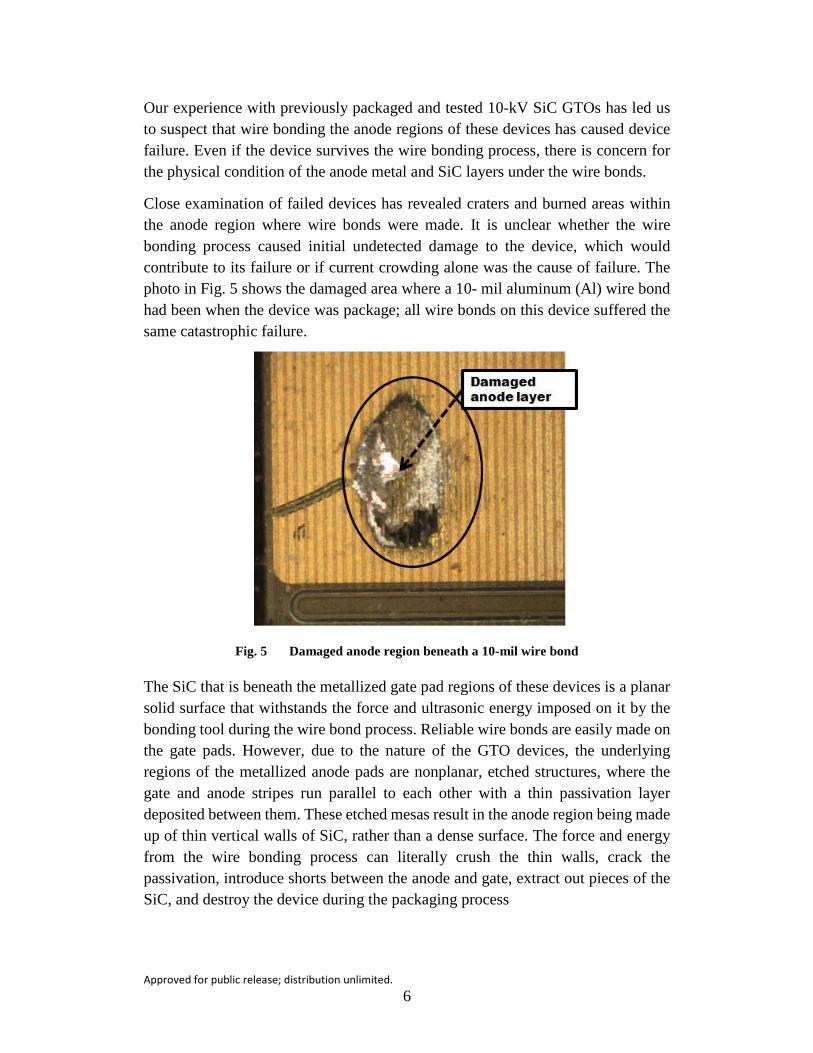
Close examination of failed devices has revealed craters and burned areas within the anode region where wire bonds were made. It is unclear whether the wire bonding process caused initial undetected damage to the device, which would contribute to its failure or if current crowding alone was the cause of failure. The photo in Fig. 5 shows the damaged area where a 10- mil aluminum (Al) wire bond had been when the device was package; all wire bonds on this device suffered the same catastrophic failure.
Fig. 5 Damaged anode region beneath a 10-mil wire bond
The SiC that is beneath the metallized gate pad regions of these devices is a planar solid surface that withstands the force and ultrasonic energy imposed on it by the bonding tool during the wire bond process. Reliable wire bonds are easily made on the gate pads. However, due to the nature of the GTO devices, the underlying regions of the metallized anode pads are nonplanar, etched structures, where the gate and anode stripes run parallel to each other with a thin passivation layer deposited between them. These etched mesas result in the anode region being made up of thin vertical walls of SiC, rather than a dense surface. The force and energy from the wire bonding process can literally crush the thin walls, crack the passivation, introduce shorts between the anode and gate, extract out pieces of the SiC, and destroy the device during the packaging process

Approved for public release; distribution unlimited. 7
The device packaged at ARL was a 10-kV SiC GTO; the top and bottom surfaces were Au plated. The gate connections were made using 0.005-inch Al wire bonds. However, copper strips were soldered to the anode regions in lieu of wire bonds for the connections due to suspected damage during the wire bonding process. This method avoids putting physical stress on the thin mesa walls with the bonding tool and eliminates the hot spots suspected from the individual wire bonds.
To achieve this, two 0.008-inch-thick copper strips were cut to approximately 0.100 inch wide for the anode connections. The width of the copper strips was chosen to make contact with as large an area of the anode as possible so current would be evenly distributed, but would maintain a sufficient distance from the passivated edges of the device.
For die attach, a 0.002-inch gold-tin (AuSn) preform was cut to 90% of the device size; industry standard dictates that an optimum size for a preform is between 85% to 90% of the die being attached. Two small pieces of AuSn preform were cut to about 80% of the copper strip area that would contact the anode to affix the copper strips to the anode regions of the device. The slightly smaller preform size was chosen to ensure enough solder was used to attach the strips without flowing into “keep-out” areas between the passivation ring or flowing too close to the gate pads.
The device and preforms were cleaned with isopropyl alcohol. The base plate, copper strips, and copper terminals were cleaned with acetone and rinsed with isopropyl alcohol. The copper strips and copper terminals underwent an additional cleaning with hydrochloric acid to ensure all oxidation was removed.
Once all the parts were prepared the 9-mm2 solder preform was placed in the center of the base plate, and the device was placed on the preform. The 2 thin strips of solder preform were positioned in the center of each anode region on the device, and the copper strips were placed on those preforms. A narrow piece of Kapton tape was used to hold all the items in place to prevent shifting during reflow. Figure 6 depicts the device and copper strips on the base plate ready to be reflowed in the furnace.

Approved for public release; distribution unlimited. 8
Fig. 6 GTO with copper strips as anode connections on the base plate ready for reflow in the furnace
The base plate containing the device and copper strips was placed in an SST vacuum reflow furnace to reflow the solder for the die attach and copper strip attachment. After reflow, a multimeter was used to ensure the solder process had not caused shorting between the anode and gate mesas.
The 0.005-inch Al wire bonds for the gate were attached to the device before the base plate was mounted to the PEEK plastic case; however, the wires were cut long and left hanging in air. The wires would be bonded to the terminal in a future step. This was a slightly different wire bonding approach due to working room limitations inside the package cavity.
Once the gate wires were placed on the device, a small bead of RTV silicone sealant was applied to the area of the case where the base plate contacts the case. The RTV prevents the encapsulation from leaking out and prevents air bubbles from forming inside the package cavity. At this point, the base plate was screwed to the case.
The free-hanging ends of the copper strips were soldered to one of the copper terminals inside the package cavity to complete the anode connection. Since the terminals were not expected to see extreme temperatures, standard Sn63 solder was used. Flux residue was cleaned off the copper with alcohol to ensure encapsulation would adhere to the surface.
Once all work was completed inside the package, the loose hanging ends of the 0.005-inch Al wire bonds from the gate pads were tacked to the other copper terminal to complete the gate connection. Figure 7 shows the complete improved package prior to encapsulation.

Approved for public release; distribution unlimited. 9
Fig. 7 Packaged device with wire bonds and copper strips attached to the terminals in the improved package
In the final step, the package was encapsulated with Sylgard 527 silicone gel. After allowing the RTV seal between the case and base plate to cure for 24 h, the device was encapsulated, ensuring enough gel was poured in the cavity to fully cover the wire bonds and copper strips on the terminals. Currently, the package base plate is made of pure copper that has been Ni/Au plated, and AuSn is used for the die attach solder. Both materials have been adequate for the devices we have packaged and tested, and both have excellent electrical and thermal conductivity and high mechanical strength. However, further advancements in SiC devices may demand using other packaging materials, especially for devices that have a larger footprint area.
One potential issue with using a pure copper base plate is the coefficient of thermal expansion (CTE) of 16.9 ppm/°C at room temperature. The SiC devices we package have a CTE of only 4, so the difference between and copper base plate and device is quite significant. Table 1 illustrates the material properties of some typical device packaging materials.

Approved for public release; distribution unlimited. 10
Table 1 Material properties of typical device packaging materials5
Material Solid at °C
CTE (ppm/°C)
Thermal conductivity
(W/mK)
Young’s modulus
(GPa) Copper (Cu) … 16.9 390 115 Copper/tungsten (W) (Cu15/W85) … 6.8 175 225 Copper/tungsten (Cu10/W90) … 6.4 195 330 SiC … 4 120 410 Gold/tin (Au80Sn20) 280 16 57 59.1 Tin-silver-copper 305 (Sn96.5/Ag3/Cu.5) 217 21.6 58 50 Tin-lead (Sn63/Pb37) 183 25 50 32 Lead-tin (Pb95/Sn5) 308 28.4 23 18.5
The next generation of our improved package will include changing the base plate material to either Cu15/W85, or Cu10/W90, whose CTEs are 6.8 and 6.4, respectively. The CTE mismatch between the SiC devices and the base plate will be greatly reduced (to a difference of less than 3 ppm/°C), which, in turn, will reduce the physical stress on the device during packaging and operation.
Though the thermal conductivity of Cu is far superior to either of the CuW alloys (390 and 175–195, respectively), the heat dissipation levels for our current requirement will be satisfied by using CuW as a base plate. Generally, when a device requires more heat transfer than a simple base plate can offer, the base plate will be attached to a heat sink.
Another approach to reducing stress on a packaged device is to use a softer, more compliant solder for the die attach.6 Where it is advantageous for the CTE of the device and the base plate or substrate to be closely matched, a ductile die attach solder will help to absorb the stress between the 2 if there is a large mismatch.
As technology advancements pave the way for larger devices to be manufactured that operate at even higher temperatures, the stress caused by CTE mismatches will become more of an issue than currently experienced. A larger device will require a die attach that can flex and expand at a greater rate as the device is pulsed, heated, and cooled repeatedly. Without compliance the stressed device may delaminate from the substrate or crack over time causing device failure.
4. Experimental Setup
The device evaluation implemented in this work investigated the wide-pulse current handling capabilities of the 1.0-cm2 SiC SGTO using the ARL-modified Cree power package. The schematic of the evaluation circuit is displayed in Fig. 8. The pulse evaluation circuit has a substantial amount of energy storage capability for evaluating advanced solid-state pulsed power devices. The amount of current

Approved for public release; distribution unlimited. 11
generated in the circuit is linearly proportional to the charge voltage on the capacitors and the current waveform is shaped by the inductor in the circuit.
Fig. 8 Circuit schematic for wide-pulse evaluation of the SiC SGTO
The SiC SGTO (device under test [DUT]) is in-line with a Solidtron Si P-i-N diode, and an additional P-i-N diode is in parallel with the capacitor and inductor. The DUT used has a closing switch and is triggered into the ON-state with a fiber-optic transmitter once the capacitor has been charged up to the desired voltage of choice with a power supply. The driver used to trigger the GTO floated at elevated voltage levels and used an isolation pulse transformer. The anode of the device was pulsed positive relative to the gate.
The high action evaluation circuit (Fig. 8) had custom-made inductors with a total inductance of approximately 180 μH. The capacitors used in circuit were three 175-µF capacitors rated for 22 kV in a parallel configuration; a total charge capacitance of 525 μF and a load resistance of 200 mΩ was used in the pulsed circuit. The primary purpose of the anti-parallel Solidtron Si diode in the circuit schematic in Fig 8 (not visible in Fig. 9) was to mitigate the reverse voltage recovery that the in-line Si diode must withstand after being subjected to an elevated current pulse.

Approved for public release; distribution unlimited. 12
Fig. 9 Image of the wide-pulse evaluation station
5. Experimental Results
Preliminary electrical analysis of the solder-based package SGTO was implemented on a Tektronix 371A high-power curve tracer before doing any pulse evaluation. Figure 10 depicts the current-voltage (I-V) characteristics of the SGTO. A negative gate current pulse was applied to the gate terminal of the device relative to the anode to cause the SGTO to latch-on.
Fig. 10 I-V characteristics of solder-based packaged SiC SGTO
The process in determining the maximum and repeatable peak current level of the SiC SGTO under wide pulse conditions consisted of gradually increasing the voltage across the charging capacitor in increments of 100 V. When the anode-to-cathode current (Iak) of the SGTO saturated, the forward voltage across the die
Cat
hode
Cur
rent
(A)
Cathode Voltage (V)
-0.140000001

Approved for public release; distribution unlimited. 13
would increase gradually after every recurring current pulse causing the device to self-heat and eventually result in a catastrophic failure. In order to prohibit device failure, the device must be pulsed at a safe repeatable current level in which the forward voltage drop of the device is stable and consistent. The wide pulse capability of the SiC SGTO is illustrated in Fig. 11. The SiC SGTO successfully conducted a 1-ms base pulse width at 2.14 kA, equating to a current density well of 3.7 kA/cm2. The pulsed I-V characterization of the SiC SGTO is depicted in Fig. 12. The SGTO was able to withstand an instantaneous peak power of 29.3 kW and power density of 50.5 kW/cm2 .
Fig. 11 Wide pulse characterization of solder-based packaged SiC SGTO
Fig. 12 Pulsed I-V characterization of solder-based packaged SiC SGTO

Approved for public release; distribution unlimited. 14
6. Conclusions
The superior switching and peak current handling capability of the SiC SGTO makes it a viable candidate for Army pulsed power applications. This research demonstrates the successful implementation of an optimized, flux-less, solder-based power package using a SiC GTO for extreme pulsed power switching conditions. The SiC GTO was pulsed up to 2.14 kA with a 1-ms pulse-width. The alternative solder-bond packaging approach process was implemented on one device. Future work will include the pulsed power performance and reliability of solder bond packaging approach on additional HV pulsed power devices greater than 10 kV.

Approved for public release; distribution unlimited. 15
7. References
1. Baliga BJ. Power devices. In: Sze SM, editor. Modern semiconductor devices physics. New York (NY): Wiley; 1998, p. 226.
2. Ogunniyi A, O’Brien H, Lelis A, Scozzie C, Shaheen W, Agarwal A, Zhang J, Callanan R, Temple V. The benefits and current progress of SiC SGTOs for pulsed power applications. Solid State Electronics. 2010;54(10):1232–1237.
3. SiC Physical & Electrical Properties. Durham (NC): Cree, Inc.; 2015 [accessed 2015 Mar]. http://www.cree.com/products/material.asp.
4. Agarwal A, Capell C, Zhang Q, Richmond J, Callanan R, O’Loughlin M, Burk A, Melcher J, Palmour J, Temple V, O’Brien H, Scozzie CJ. 9 kV, 1 × 1cm SiC super GTO technology development for pulse power. Proc. 17th IEEE PPC; 2009; Washington, DC. p. 264–269.
5. McCluskey FP, Grzybowski RR, Podlesak TF, eds. High temperature electronics. Boca Raton (FL): CRC Press; 1996.
6. Manikam VR, Kuan YC. Die attach materials for high temperature applications: a review. IEEE Trans Components, Packaging and Manufacturing Tech. 2011:457–478.

Approved for public release; distribution unlimited. 16
List of Symbols, Abbreviations, and Acronyms
Ag silver
Al aluminum
ARL US Army Research Laboratory
Au gold
Cu copper
DUT device under test
GTO gate-turn-off thyristor
HV high-voltage
I-V current-voltage
JTE junction termination edge
Ni nickel
PEEK package included a polyetheretherketone
RTV room temperature vulcanization
SGTO “super” gate-turn-off thyristors
Si silicon
SiC silicon carbide
Sn tin
Ti titanium
W tungsten

Approved for public release; distribution unlimited. 17
1 DEFENSE TECH INFO CTR (PDF) DTIC OCA 2 US ARMY RSRCH LAB (PDF) IMAL HRA MAIL & RECORDS MGMT RDRL CIO L TECHL LIB 1 GOVT PRNTG OFC (PDF) A MALHOTRA 5 US ARMY RSRCH LAB (PDF) RDRL SED P A OGUNNIYI D IBITAYO H O’BRIEN B GEIL C TIPTON IV

Approved for public release; distribution unlimited. 18
INTENTIONALLY LEFT BLANK