advances in analog circuit design 2014 the ring amplifier: scalable amplification with ring...
TRANSCRIPT

Advances in Analog Circuit Design 2014
The Ring Amplifier: Scalable Amplification with Ring
Oscillators
Benjamin Hershberg1, Un-Ku Moon2
1 imec Leuven, Belgium2 Oregon State University Corvallis, USA
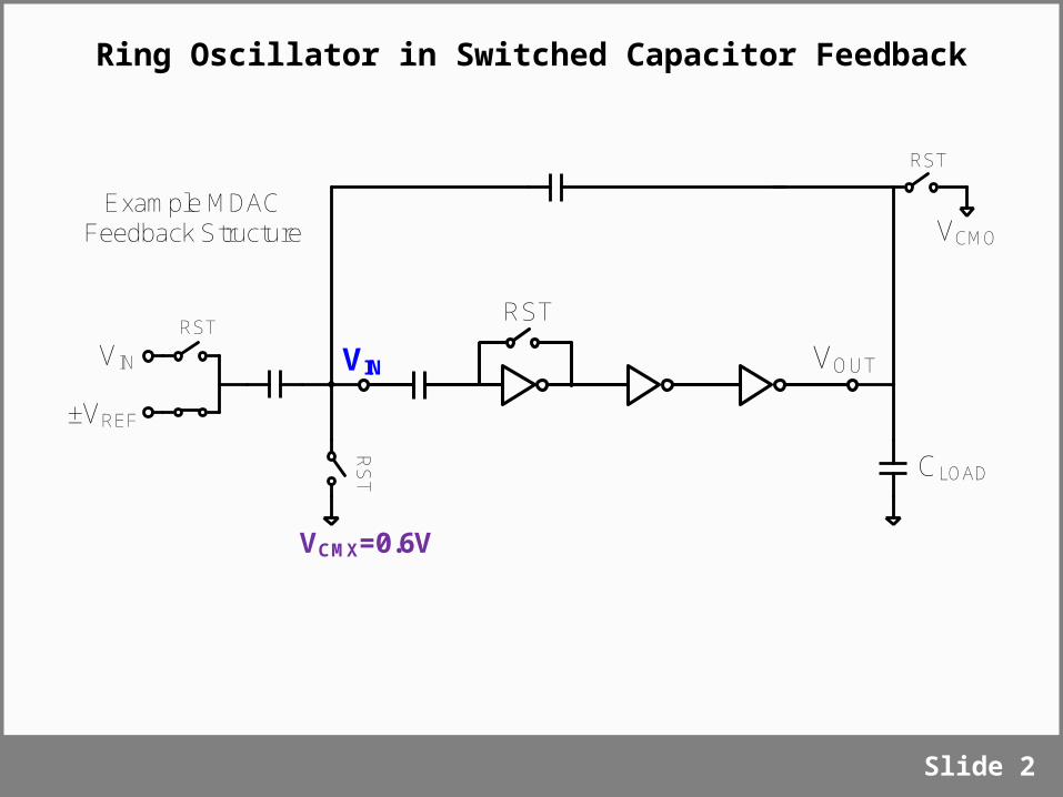
Ring Oscillator in Switched Capacitor Feedback
RS
T
VCMX=0.6V
VIN
±VREF
CLOAD
RST
RST
VCMO
Example MDAC Feedback Structure
VIN VOUT
RST
Slide 2
0 1 2 3 4 5 6
0
0.2
0.4
0.6
0.8
1
1.2
Vol
ts
time (ns)
1.2
1
0.8
0.6
0.4
0.2
00 1 2 3 4 5 6
Volt
s
time (ns)
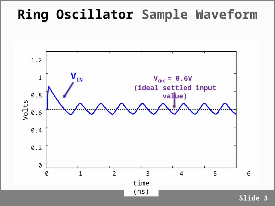
Ring Oscillator Sample Waveform
VCMX = 0.6V (ideal settled input
value)
VIN
Slide 3

Ring Oscillator: The Perfect Switch-Cap Amplifier?
• High frequency poles, large bandwidth• Rail to rail swing• Maximal slewing efficiency• Small, simple layout• High cascaded gain• Inherent class-AB behavior• Fully compatible with digital CMOS
Slide 4
CL
VOUTVIN
Feedback network
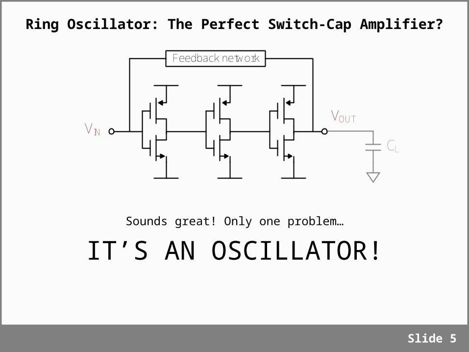
IT’S AN OSCILLATOR!
Slide 5
CL
VOUTVIN
Feedback network
Sounds great! Only one problem…
Ring Oscillator: The Perfect Switch-Cap Amplifier?

Oscillator / Amplifier duality
Slide 6Slide 6Slide 6
Any unstable ring oscillator can become a stable amplifier

Slide 7
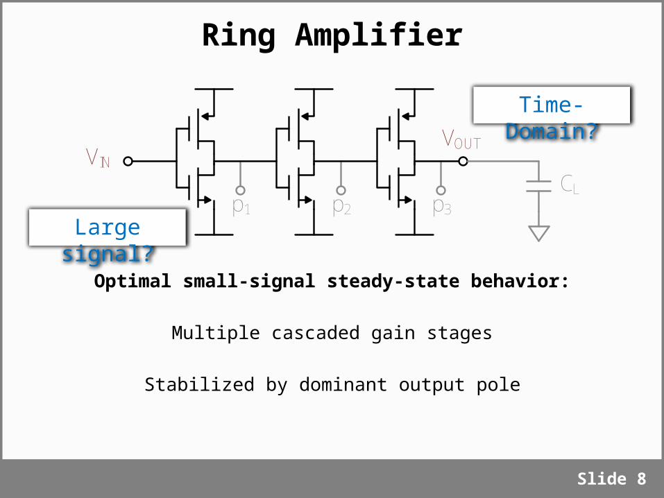
Small-signal three stage amplifier
p1 p2 p3
VOUT
CL
VIN
Optimal configuration:
dominant pole p3
Ring Amplifier
Slide 8
Optimal small-signal steady-state behavior:
Multiple cascaded gain stages
Stabilized by dominant output pole
p1 p2 p3
VOUT
CL
VIN
Large signal?
Time-Domain?

Ring Amplifier: Basic Theory
RS
T
VCMX
VIN
±VREF
CLOAD
RST
RST
VCMO
Example MDAC Feedback Structure
-VDZ
+
RST RST
RST
-VOS+
+VOS-
• Split signal into two separate paths• Embed offset in each path
Slide 9

0 1 2 3 4 5 6
0
0.2
0.4
0.6
0.8
1
1.2
Vol
ts
time (ns)
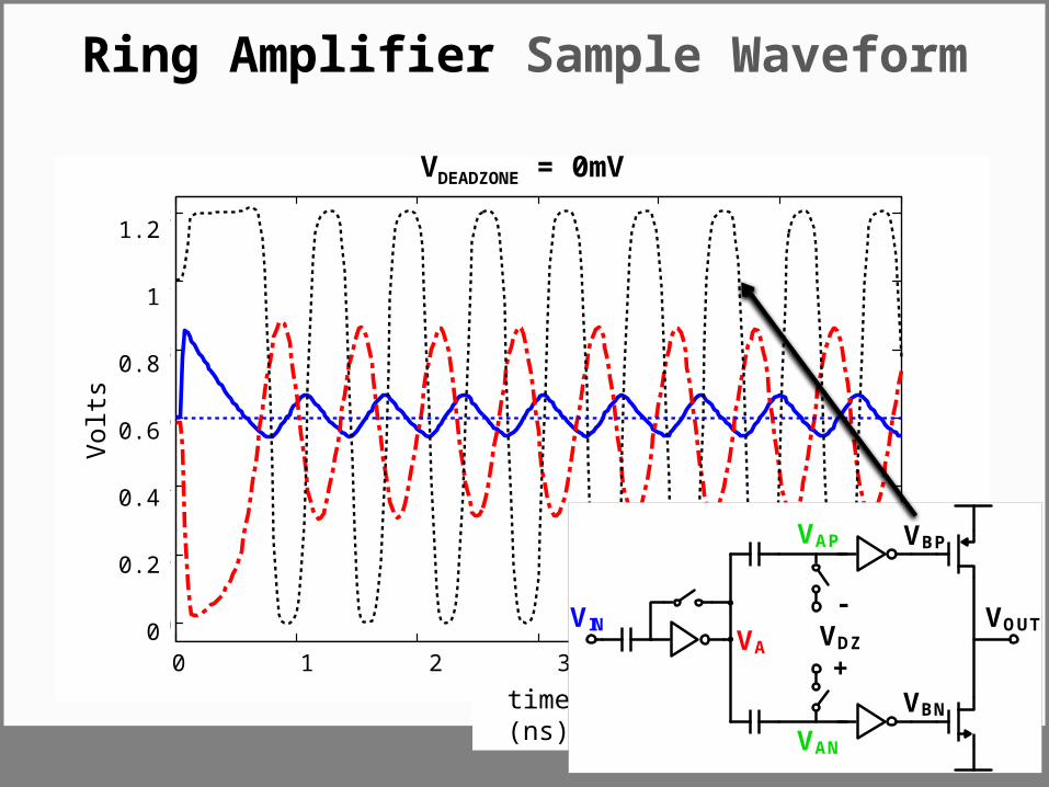
Ring Amplifier Sample Waveform
VDEADZONE = 0mV
1.2
1
0.8
0.6
0.4
0.2
00 1 2 3 4 5 6
Volt
s
time (ns)
10
-VDZ
+
VAN
VIN VOUTVA
VBP
VBN
VAP

0 1 2 3 4 5 6
0
0.2
0.4
0.6
0.8
1
1.2
Vol
ts
time (ns)
Ring Amplifier Sample Waveform
VDEADZONE = 0mV
1.2
1
0.8
0.6
0.4
0.2
00 1 2 3 4 5 6
Volt
s
time (ns)
11
-VDZ
+
VAN
VIN VOUTVA
VBP
VBN
VAP
0 1 2 3 4 5 6
0
0.2
0.4
0.6
0.8
1
1.2
Vol
ts
time (ns)
Ring Amplifier Sample Waveform
VDEADZONE = 0mV
1.2
1
0.8
0.6
0.4
0.2
00 1 2 3 4 5 6
Volt
s
time (ns)
12
-VDZ
+
VAN
VIN VOUTVA
VBP
VBN
VAP

0 1 2 3 4 5 6
0
0.2
0.4
0.6
0.8
1
1.2
Vol
ts
time (ns)
Ring Amplifier Sample Waveform
VDEADZONE = 0mV
1.2
1
0.8
0.6
0.4
0.2
00 1 2 3 4 5 6
Volt
s
time (ns)
13
-VDZ
+
VAN
VIN VOUTVA
VBP
VBN
VAP

0 1 2 3 4 5 6
0
0.2
0.4
0.6
0.8
1
1.2
Vol
ts
time (ns)
Ring Amplifier Sample Waveform
VDEADZONE = 200mV
1.2
1
0.8
0.6
0.4
0.2
00 1 2 3 4 5 6
Volt
s
time (ns)
Slide 14

0 1 2 3 4 5 6
0
0.2
0.4
0.6
0.8
1
1.2
Vol
ts
time (ns)
Ring Amplifier Sample Waveform
VDEADZONE = 250mV
1.2
1
0.8
0.6
0.4
0.2
00 1 2 3 4 5 6
Volt
s
time (ns)
Slide 15

0 1 2 3 4 5 6
0
0.2
0.4
0.6
0.8
1
1.2
Vol
ts
time (ns)
Ring Amplifier Sample Waveform
VDEADZONE = 300mV
1.2
1
0.8
0.6
0.4
0.2
00 1 2 3 4 5 6
Volt
s
time (ns)
Slide 16

0 1 2 3 4 5 6
0
0.2
0.4
0.6
0.8
1
1.2
Vol
ts
time (ns)
Ring Amplifier Sample Waveform
VDEADZONE = 350mV
1.2
1
0.8
0.6
0.4
0.2
00 1 2 3 4 5 6
Volt
s
time (ns)
Slide 17

0 1 2 3 4 5 6
0
0.2
0.4
0.6
0.8
1
1.2
Vol
ts
time (ns)
Ring Amplifier Sample Waveform
VDEADZONE = 400mV
1.2
1
0.8
0.6
0.4
0.2
00 1 2 3 4 5 6
Volt
s
time (ns)
Slide 18

What is the “Stability Region”?
Slide 19
VIN -VDZ1+
VOUT
RST RST
RSTC3
C2
MCP
MCNVTEST
IOUT
• VDZ1 large
– Dead-zone: Class-B– Distortion limits accuracy
• VDZ1 small
– Weak-zone: Class-AB– Only finite gain limits accuracy– Gain and output swing
advantage
-4 -2 0 2 4
-0.2
-0.1
0
0.1
0.2
Vin
pk-pk(mV)
I out(m
A)
DCsweepofVin
vsIout
CoarseRingampFineRingamp
StabilityRegion
Dead-zone
Weak-zone
[Hershberg, VLSI 2013]
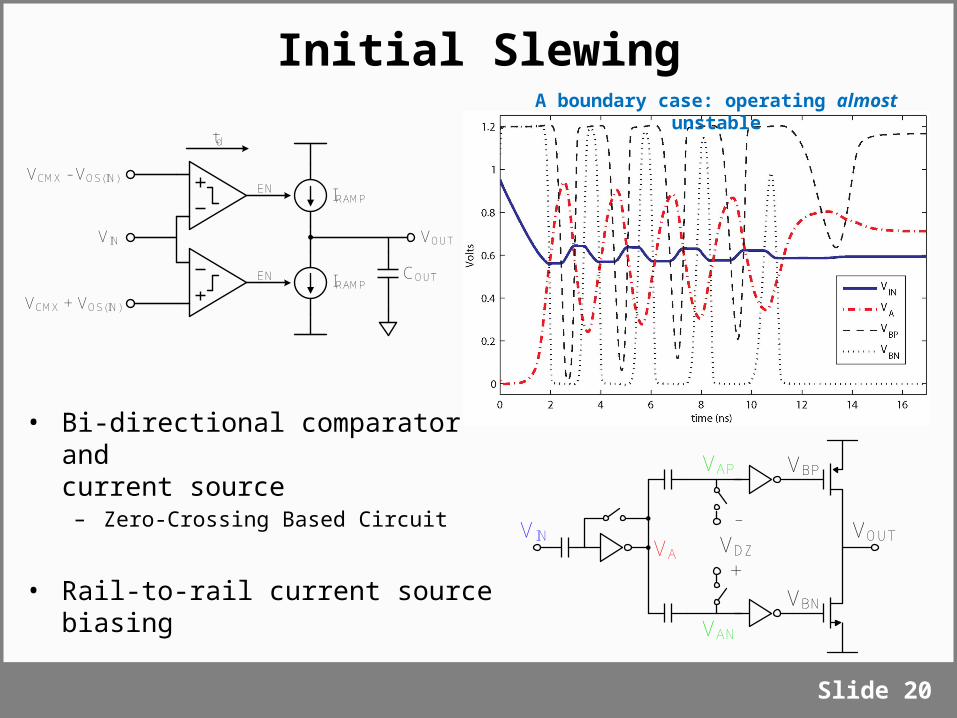
Initial Slewing
• Bi-directional comparator and current source
– Zero-Crossing Based Circuit
• Rail-to-rail current source biasing
Slide 20
VIN
VCMX - VOS(IN)
IRAMP
VOUT
EN
EN
VCMX + VOS(IN)
td
COUTIRAMP
-VDZ
+
VAN
VIN VOUTVA
VBP
VBN
VAP
A boundary case: operating almost unstable

Stabilization
Slide 21
AV2*(VIN*AV1 + VOS)
AV2*(VIN*AV1 - VOS)
-VDZ
+
VIN VOUT
AV1
AV2
+VOS-
-VOS+

-VDZ
+
VAN
VIN VOUTVA
VBP
VBN
VAP
Slide 22
+VOS
-
-VOS+
VDD/2
VDD/2 - VOS
VDD/2
VDD/2 + VOS
Stabilization
Separate signal paths: gain-limited output swing for large input swing.

Stabilization
Slide 23
-VDZ
+
VAN
VIN VOUTVA
VBP
VBN
VAP1. Reduced avg. overdrive
voltage2. Reduced output slew rate3. Reduced oscillation amplitude4. Gain-limited internal swings
A boundary case: operating almost unstable
AV2*(VIN*AV1 + VOS)
AV2*(VIN*AV1 - VOS)
-VDZ
+
VIN VOUT
AV1
AV2
+VOS-
-VOS+

Stabilization
• Slew limited gain• During stabilization
– Small VA/VIN
• During steady-state– Large VA/VIN
• Enhances accuracy/speed tradeoff
Slide 24
-VDZ
+
VAN
VIN VOUTVA
VBP
VBN
VAP
VINVAA more subtle secondary effect…
A boundary case: operating almost unstable

Stabilization
Slide 25
1) Offset embedding creates a large signal finite gain effect
2) Large signal finite-gain effect strengthens with non-linear time feedback
3) Dynamically shifts small signal pole, granting stability and gain

Ring Amplifier Core Benefits
Exponential dynamic stabilization• Very fast• Well defined tradeoffs
26

Ring Amplifier Core Benefits
Slew-based charging• Charges with maximally biased, digitally-switched current
sources– VGS = VDD
– Can be very small, even for large CLOAD
– Decouples internal speed vs. output load requirements
27
VIN -VDZ1+
VOUT
RST RST
RSTC3
C2
MCP
MCN
CL
Rail-to-rail inverters+
-
+-
Max VOV
Max VOV
Very small transistors

Ring Amplifier Core Benefits
Scalability (Speed/Power)• Internal speed/power (mostly) independent of CLOAD
– Inverter td, crowbar current, parasitic C’s
– Digital power-delay product scaling benefits apply
• Power/speed product scales with digital process trends
28

Ring Amplifier Core Benefits
Scalability (Output Swing / SNR)• Compression immune: rail-to-rail output swing
– VOV pinchoff: decreases VDSAT, decreses ID, increases ro
29
VIN -VDZ1+
VOUT
RST RST
RSTC3
C2
MCP
MCN
small VOV = VGS-VT +
-
+
-small VOV = VGS-VT
Low frequency output pole
+
-Large ro,small VDSAT
+
-Large ro,small VDSAT
Dynamic biasing = wide, compression free output swing

Ringamp Implementations
Slide 30Slide 30Slide 30

Survey of Ringamp Structures
Slide 31
Basic Proof of Concept High-resolution
High-resolution (ringamp only) Nanoscale
CMOS improvements

Coarse Ringamp
Slide 32Slide 32Slide 32
10.5b Pipelined ADCHershberg, VLSI 2012
[Hershberg, VLSI 2012]

Coarse Ringamp Prototype
• Basic ringamp prototype– Minimum size transistors– Rail-to-rail output swing– Good noise performance
Slide 33
VIN VOUT
VRN
Φrst
Φrst
Φrst
VRP
840nm160nm
840nm160nm
320nm160nm
320nm160nm
960nm320nm
320nm320nm
320nm160nm
320nm160nm2.52µm
240nm
960nm240nm
320nm160nm
100fF
100fF
MCP
MCN
C2
C3100fF
C1
VA
[Hershberg, VLSI 2012]

Split-CLS
Slide 34Slide 34Slide 34
15b Pipelined ADCHershberg, ISSCC 2012
[Hershberg, ISSCC 2012]

Split-CLS (Correlated Level Shifting)
• Split-CLS: Gain Enhancement Technique
Slide 35
VO+C-RAMP
VO-RAMP
opamp CMFB
Vi+
Vi-
CoarseRAMP
CoarseRAMP
ΦCLS
VCM
CCLS
CCLS
[Hershberg, ISSCC 2012]

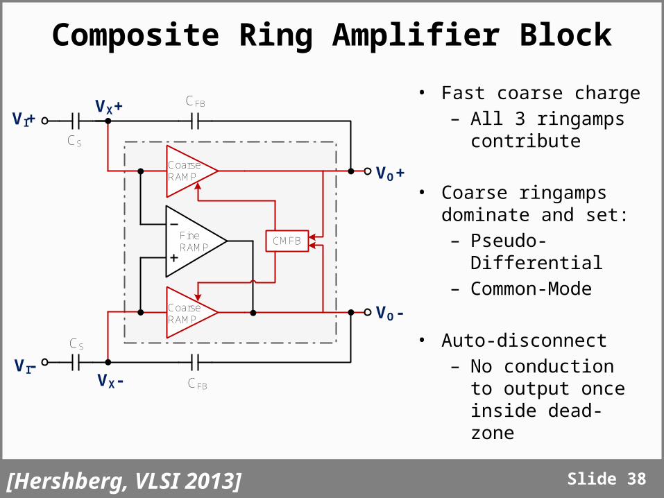
Composite Ring Amplifier Block
Slide 36Slide 36Slide 36
15b Pipelined ADC
[Hershberg, VLSI 2013]

Composite Ring Amplifier Block
Slide 37
• Composite Ring Amplifier Block
• Coarse– 2 Class-B
ringamps
• Fine– 1 Class-AB
ringamp
VO+CoarseRAMP
CoarseRAMP
FineRAMP
CMFB
VX+
VX-
VI+
VI-
CS
CFB
CS
CFB
VO-
[Hershberg, VLSI 2013]
Composite Ring Amplifier Block
Slide 38
VO+CoarseRAMP
CoarseRAMP
FineRAMP
CMFB
VX+
VX-
VI+
VI-
CS
CFB
CS
CFB
VO-
• Fast coarse charge– All 3 ringamps
contribute
• Coarse ringamps dominate and set:– Pseudo-
Differential– Common-Mode
• Auto-disconnect– No conduction to
output once inside dead-zone
[Hershberg, VLSI 2013]

Composite Ring Amplifier Block
Slide 39
VO+CoarseRAMP
CoarseRAMP
FineRAMP
CMFB
VX+
VX-
VI+
VI-
CS
CFB
CS
CFB
VO-
• Fine settle– VO+ floating
– VO- connected
– Common-mode ok
• Detect differentially, charge single-ended– VO- settles around
a floating VO+
[Hershberg, VLSI 2013]

Composite Ring Amplifier Block
Slide 40
Coarse ringamp dead-zone
[Hershberg, VLSI 2013]

Composite Ring Amplifier Block
Slide 41[Hershberg, VLSI 2013]

Class-AB Ringamp Structure
• Offset embedded between stages 2 and 3
• Guarantees weak-inversion– Enhanced Gain– Wide Output Swing
Slide 42
VOUT
C2
MCP
MCN
C3
+VDZ2
-
VIN+ +
-VIN- C1
A1 A2
RGC
A3
[Hershberg, VLSI 2013]
Reduced slewing efficiency…

Composite Ring Amplifier Block
Slide 43
VO+CoarseRAMP
CoarseRAMP
FineRAMP
CMFB
VX+
VX-
VI+
VI-
CS
CFB
CS
CFB
VO-
[Hershberg, VLSI 2013]
• High accuracy ADC using only ringamps• Maximum scalability

Self-Biased Ring Amplifier
Slide 44Slide 44Slide 44
10.5b Pipelined ADCLim, ISSCC 2014
[Lim, ISSCC 2014]

VOUT
CL
VIN RB
• Dynamic pole adjustment using only RB
• Initial slew, VOS = 0V– Max overdrive, max efficiency
• VOS dynamically grows during stabilization
Slide 45[Lim, ISSCC 2014]
Setting Stability Region with a Resistor
+VOS
-

Ring oscillators do make great amplifiers!
→ Slewing
→ Output Swing
→ Bandwidth
→ Gain
→ Scaling benefit
Slide 46
Small Signal
Large Signal
Transient

Where Next?
Slide 47
Anything clocked with a capacitive load …
Discrete Time FiltersDT Sigma-Delta
Etc.
Time to re-examine some old assumptions…

Thank you for your attention.
Slide 48