advanced radio frequency energy harvesting with power
TRANSCRIPT
Progress In Electromagnetics Research B, Vol. 89, 45–62, 2020
Advanced Radio Frequency Energy Harvesting with PowerManagement from Multiple Sources for Low Power Sensors
and Mobile Charging Applications
Manee Sangaran1, *, Agileswari Ramasamy2, and Norashidah Md Din1
Abstract—A complete energy harvesting system via Radio Frequency (RF) is designed in a broadcaststation where multiple frequency sources are readily available. These frequency sources are theIntermediate Frequency (IF), 70 MHz, Wi-Fi frequency band, 2.4 GHz, and the Ku-band frequency,13 GHz. The RF source via the Wi-Fi band (2.4 GHz) is harvested via a microstrip patch antennadesigned with its matching network. The harvested RF energy is transformed into usable DC power viaan 8-stage Villard voltage doubler circuit. The DC power is managed by a power management systemhandled by the BQ25570 circuit which gives a regulated output of 3 V, powers up a low power motionsensor, and charges a battery at the same time. This system comes with a backup source which is thebattery and able to take over the system in case the incoming RF signal fails. The RF energy harvestedfrom the IF 70 MHz and Ku-band at 13 GHz is derived from coupler outputs which are available inbroadcast stations, transmission lines, etc. Both these RF signals are converted to DC signals via a5-stage Villard voltage doubler circuit with different matching networks. The DC power is managed bya power mux via the TPS2122 which selects the highest available power. Over the years, no works onRF harvesting have focused on smart phone charging as its application, due to the limitation in poweravailability. This work strives to provide enough power to charge phones and effectively gives a 5 Voutput to charge smart phones with a charging current of 0.5 A which is similar to a USB charging port.
1. INTRODUCTION
During the recent times, a number of research works have been done on RF energy harvesting wherebyRF energy from surroundings is captured and converted into DC power for low power applications [1].Various methods of RF energy scavenging have been discovered over the years to make use of this readilyavailable energy source. The core idea of this harvesting method is that the RF energy is scavengedwith a microstrip patch antenna and transformed into DC power via some sort of rectifier circuit.The DC is then regulated and managed by a power management circuit [2]. This method of energyharvesting best works on networks with limited power. One of such networks would be wireless sensornetworks. A major drawback here is that wireless sensor networks have a limited battery lifetime, andthis energy harvesting method can be utilized to power up these sensors in return eliminating the usageof batteries [3]. Most of the researches have covered on capturing RF signals from the ambience andat low frequency. This work extensively concentrates on harvesting RF energy from the ambience andas well as low and high frequency sources which are the Wi-Fi 2.4 GHz, IF 70 MHz, and also Ku-band13 GHz. For this, a broadcast station is chosen, and the RF sources available here are harvested andconverted into DC power. The same concept can be applied to other broadcast stations or transmission
Received 30 July 2020, Accepted 23 September 2020, Scheduled 9 October 2020* Corresponding author: Manee Sangaran(manee [email protected]).1 College of Graduate Studies, University Tenaga Nasional, Malaysia. 2 Institute of Power Engineering, University Tenaga Nasional,Malaysia.
46 Sangaran, Ramasamy, and Din
sites, whereby RF energy is readily available [4]. No research has been done via this harvesting method,and this work successfully harvests RF energy from multiple sources to power up a low power sensorand is also used to charge smart phones. Results and analysis are discussed based on the RF energyharvesting system designed.
2. THEORETICAL FRAMEWORK
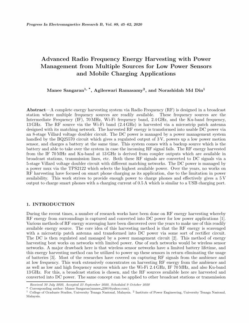
A basic RF energy harvesting system would have an antenna, a matching network, and some sort ofrectifier circuit for energy conversion. RF energy is captured via the antenna, and a matching networkis included to ensure the impedances match. Maximum power transfer is observed. This RF energy isthen converted into DC power. The Wi-Fi energy is easily accessible in many areas nowadays. Since thiswork focuses in a broadcast station, the Wi-Fi energy will be captured from the data center rooms aswell as broadcast equipment rooms as the Wi-Fi signal strength is measured to be high in these areas.Figure 1 depicts the RF energy harvesting prototype designed to capture energy from the 2.4 GHzfrequency band.
E-shaped microstrippatch antenna on 2.4 GHz Rectifier circuit Matching network
BQ25570 powermanagement
Figure 1. Signal flow for 2.4 GHz Wi-Fi frequency band harvesting system.
To harvest the signals from 2.4 GHz, an E-shaped microstrip patch antenna was designed. Theimpedance of the antenna and the RF to DC circuit is matched via a matching network circuit toensure proper power transfer. An 8-stage Villard voltage doubler circuit is designed to transform theRF to usable DC. The DC output is then connected to the Texas Instruments BQ25570 circuit. Thepower management circuit boosts the input DC power and supplies a regulated output to the loadand charges a rechargeable battery simultaneously. When there is no incoming RF or DC supply,the battery will continue to provide power to the load. This regulated DC output from the powermanagement circuit is utilized to power up a motion sensor.
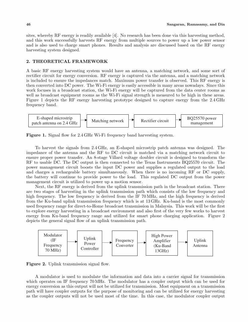
Next, the RF energy is derived from the uplink transmission path in the broadcast station. Thereare two stages of harvesting in the uplink transmission path which consists of the low frequency andhigh frequency. The low frequency is derived from the IF 70 MHz, and the high frequency is derivedfrom the Ku-band uplink transmission frequency which is at 13 GHz. Ku-band is the most commonlyused frequency range for direct-to-Home broadcast transmission in Malaysia. This work will be the firstto explore energy harvesting in a broadcast environment and also first of the very few works to harvestenergy from Ku-band frequency range and utilized for smart phone charging application. Figure 2depicts the general signal flow of an uplink transmission path.
Modulator (IF
Frequency 70 MHz)
Uplink Power
Controller
Frequency Converter
High PowerAmplifier (Ku-Band
13GHz)
Uplink Antenna
Figure 2. Uplink transmission signal flow.
A modulator is used to modulate the information and data into a carrier signal for transmissionwhich operates on IF frequency 70 MHz. The modulator has a coupler output which can be used forenergy conversion as this output will not be utilized for transmission. Most equipment on a transmissionpath will have coupler outputs for the purpose of monitoring and can be utilized for energy harvestingas the coupler outputs will not be used most of the time. In this case, the modulator coupler output
Progress In Electromagnetics Research B, Vol. 89, 2020 47
gives an IF 70 MHz at a constant power level of +10 dBm. Since the RF signal is readily available, anantenna will not be required, and the RF signal can be fed directly into the rectifier circuit to producethe DC power.
The uplink power controller is responsible for controling the transmission power to the satellite.Since the transmission is on Ku-band frequency, which is prone to rain, a higher transmission poweris required during rain to mitigate rain fade and ensure that the RF signal reaches the satellite. Thefrequency converter is used to convert the IF 70 MHz frequency to Ku-band frequency. The Ku-bandfrequency is then fed to the High-Power Amplifier (HPA) which is used to boost the uplink power incase of rain. The HPA’s output power varies based on the weather condition and will boost to 2000 Win case of rain which will be controlled by the uplink power controller. The HPAs have a coupler outputas well which gives the Ku-band 13 GHz output which will be used for harvesting. The power levelfrom this coupler was measured to be at +0dBm during clear sky weather conditions and can go up to+30 dBm during rain.
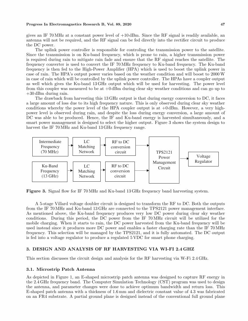
The drawback from harvesting this 13 GHz output is that during energy conversion to DC, it facesa large amount of loss due to its high frequency nature. This is only observed during clear sky weatherconditions whereby the power level of the HPA coupler output is at +0dBm. However, a very high-power level is observed during rain, and despite the loss during energy conversion, a large amount ofDC was able to be produced. Hence, the IF and Ku-band energy is harvested simultaneously, and asmart power management is designed to select the higher output. Figure 3 shows the system design toharvest the IF 70 MHz and Ku-band 13 GHz frequency range.
IntermediateFrequency (70 MHz)
Ku-Band Frequency(13 GHz)
LCMatching Network
RF to DCconversion
circuit
RF to DCconversion
circuit
LCMatching Network
TPS2121Power
ManagementCircuit
VoltageRegulator
Figure 3. Signal flow for IF 70 MHz and Ku-band 13 GHz frequency band harvesting system.
A 5-stage Villard voltage doubler circuit is designed to transform the RF to DC. Both the outputsfrom the IF 70 MHz and Ku-band 13 GHz are connected to the TPS2121 power management interface.As mentioned above, the Ku-band frequency produces very low DC power during clear sky weatherconditions. During this period, the DC power from the IF 70 MHz circuit will be utilized for themobile charging. When it starts to rain, the DC power harvested from the Ku-band frequency will beused instead since it produces more DC power and enables a faster charging rate than the IF 70 MHzfrequency. This selection will be managed by the TPS2121, and it is fully automated. The DC outputis fed into a voltage regulator to produce a regulated 5 VDC for smart phone charging.
3. DESIGN AND ANALYSIS OF RF HARVESTING VIA WI-FI 2.4 GHZ
This section discusses the circuit design and analysis for the RF harvesting via W-Fi 2.4 GHz.
3.1. Microstrip Patch Antenna
As depicted in Figure 1, an E-shaped microstrip patch antenna was designed to capture RF energy inthe 2.4 GHz frequency band. The Computer Simulation Technology (CST) program was used to designthe antenna, and parameter changes were done to achieve optimum bandwidth and return loss. ThisE-shaped patch antenna with a thickness of 1.6 mm and dielectric constant value of 4.3 was fabricatedon an FR4 substrate. A partial ground plane is designed instead of the conventional full ground plane

48 Sangaran, Ramasamy, and Din
to achieve better performance on the antenna. Using Equation (1), the antenna’s effective dielectricconstant εreff was calculated [5].
For W/h > 1
εreff =εr + 1
2+
εr − 12
[1 + 12
h
W
]−1/2
(1)
The length extension, ΔL, is defined as a function of the width-to-height ratio (W/h) and alsothe effective dielectric constant εreff . The length extension ΔL is basically the dimensions of the patchalong its length that is caused by fringing effects on the xy-plane. The center frequency (fr) of theantenna is associated with the length (L) of the antenna which is calculated using Equations (2) and(3)
L =τ
2− ΔL =
12fr
√μ0ε0
√εreff
− 2ΔL (2)
where
ΔL = 0.412XhX
(εreff + 0.3)(
W
h+ 0.264
)
(εreff − 0.258)(
W
h+ 0.8
) (3)
The antenna’s bandwidth and impedance are associated with the width (W ). It is defined in terms ofthe substrate dielectric constant and the resonant frequency of the antenna where v0 is the speed oflight. Equation (4) was used to determine the width.
W =1
2fr√
μ0ε0
√2
εr + 1=
v0
2fr
√2
εr + 1(4)
The microstrip patch antenna equations were used to obtain the dimensions of the antenna, and twohorizontal slots were introduced on the patch for fringing effects in order to optimize the performanceof the antenna [6]. The feed line was strategically placed to ensure that an efficient return loss wasachieved through this design. An SMA connector is placed at the output of the antenna in order to testthe performance of the antenna.
Figure 4 shows the design of the antenna on CST.
Figure 4. Design of E-shaped microstrip patch antenna on CST.
The measurements of the antenna were computed using the antenna equations as discussed above.Two slots were introduced to induce fringing effects, and the designed antenna was optimized to obtainthe desired return loss and antenna bandwidth. Table 1 depicts the dimensions of the antenna.
Progress In Electromagnetics Research B, Vol. 89, 2020 49
Table 1. Measurements of E-shaped microstrip patch antenna.
Element Parameter Measurement (mm)
Patch Antenna Width 32Length 20
E-SlotSlot 1 Width 0.5
Length 18
Slot2 Width 0.5Length 15
Feed Line Width 1Length 16.5
Ground Plane Width 38Length 0.3
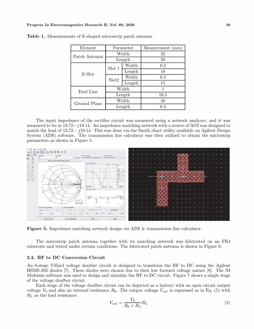
The input impedance of the rectifier circuit was measured using a network analyzer, and it wasmeasured to be at 13.72−j19.14. An impedance matching network with a source of 50 Ω was designed tomatch the load of 13.72− j19.14. This was done via the Smith chart utility available on Agilent DesignSystem (ADS) software. The transmission line calculator was then utilized to obtain the microstripparameters as shown in Figure 5.
Figure 5. Impedance matching network design via ADS & transmission line calculator.
The microstrip patch antenna together with its matching network was fabricated on an FR4substrate and tested under certain conditions. The fabricated patch antenna is shown in Figure 6.
3.2. RF to DC Conversion Circuit
An 8-stage Villard voltage doubler circuit is designed to transform the RF to DC using the AgilentHSMS-282 diodes [7]. These diodes were chosen due to their low forward voltage nature [8]. The NIMultisim software was used to design and simulate the RF to DC circuit. Figure 7 shows a single stageof the voltage doulber circuit.
Each stage of the voltage doulber circuit can be depicted as a battery with an open circuit outputvoltage V0 and also an internal resistance R0. The output voltage Vout is expressed as in Eq. (5) withRL as the load resistance.
Vout =V0
R0 + RLRL (5)

50 Sangaran, Ramasamy, and Din
Figure 6. Fabricated E-shaped microstrip patch antenna together with the partial ground plane.
Figure 7. Single stage voltage doulber circuit.
These circuits are connected into series with a load resistance RL. Then, Vout is obtained as in Eq. (6)where n is the number of stages of these circuits which are connected in series.
Vout =nV0
nR0 + RLRL = V0
1R0
RL+
1n
(6)
The rectifier components are as shown in Table 2. The circuit was fabricated on an FR4 substratewith two SMA connectors as input and output for testing purposes. Figure 8 shows the fabricatedrectifier circuit.
Table 2. Rectifier circuit components.
Component TypeDiodes Agilent HSMS-282
Stage Capacitor 100 µFFilter Capacitor 100 nFLoad Resistor 50 kΩ

Progress In Electromagnetics Research B, Vol. 89, 2020 51
Figure 8. Fabricated rectifier circuit.
3.3. Power Management
As shown in Figure 9, the Texas Instruments (TI) BQ25570 is incorporated as a power managementcircuit for this system. The BQ25570 is equipped with an adjustable Maximum Power Point Tracking(MPPT) [9] algorithm which makes sure that the input voltage does not decrease under 50% or 80%of the earlier open circuit voltage. The input voltage (VIN) is sampled based on the voltage reference(VREF SAMP). Values of external resistors (ROC1&ROC2) were calculated to ensure that the exactratio for MPPT is optimized based on Equation (7) as below:
V REFSAMP = V INDC
(ROC1
ROC1+ROC2
) (7)
Besides that, the BQ25570 has a regulated boost converter output (VOUT ), which will be used to powerup the low power sensor. The external resistors (ROUT1&ROUT2) values were calculated to set VOUT
Figure 9. BQ25570 circuitry design.
52 Sangaran, Ramasamy, and Din
as 3 V based on Equation (8) where VBIAS is nominally 1.21 V as per datasheet of the BQ255570.
VOUT = VBIAS
(ROUT1 + ROUT2
ROUT1
)(8)
The BQ25570 is also programmed to charge a rechargeable battery (VBAT ) and at the same timeprovide a regulated output. The battery has an overvoltage protection whereby charging is stopped incase battery is overcharged. The external resistors (ROV 1&ROV 2) are calculated based on Equation (9)whereby VBATOV
, the overvoltage protection value, is set to 4.2 V.
VBATOV=
32VBIAS
(1 +
ROV 2
ROV 1
)(9)
If there is no DC power at the incoming of the circuit, the battery would take over the circuit andprovide the regulated output to constantly provide power to the low power sensor. This means thatthere will be no interruption of power supply to the sensor. The IC also has a very low cold startvoltage condition which is 330 mV and is easily doable from RF to DC conversion circuit. The internalcapacitor (VSTOR) is initially charged up to 4.2 V, which powers up the boost controller. Once VSTOR
is fully charged, input as low as 100 mV is sufficient to operate the circuit.The BQ25570 is designed to produce a constant regulated voltage of 3 V. The output of the power
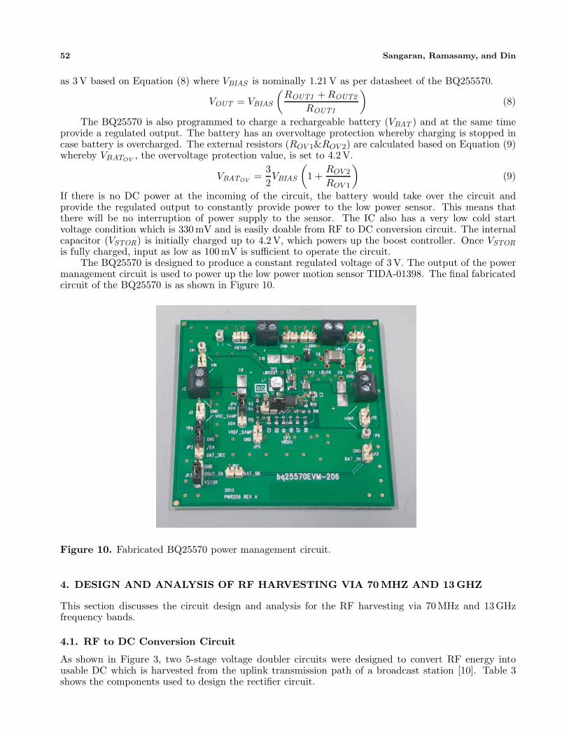
management circuit is used to power up the low power motion sensor TIDA-01398. The final fabricatedcircuit of the BQ25570 is as shown in Figure 10.
Figure 10. Fabricated BQ25570 power management circuit.
4. DESIGN AND ANALYSIS OF RF HARVESTING VIA 70 MHZ AND 13 GHZ
This section discusses the circuit design and analysis for the RF harvesting via 70 MHz and 13 GHzfrequency bands.
4.1. RF to DC Conversion Circuit
As shown in Figure 3, two 5-stage voltage doubler circuits were designed to convert RF energy intousable DC which is harvested from the uplink transmission path of a broadcast station [10]. Table 3shows the components used to design the rectifier circuit.

Progress In Electromagnetics Research B, Vol. 89, 2020 53
Table 3. Components on the rectifier circuit for harvesting 70 MHz and 13 GHz signals.
Component 70 MHz 13 GHzDiodes Skyworks CLA4601-000 Skyworks SMS7621
Stage Capacitor 0.1 µF 100 µFFilter Capacitor 100 nF 100 pFLoad Resistor 50 kΩ 50 kΩ
The capacitors were carefully selected based on the input frequency and also the peak voltagerating. The diodes are chosen depending on the input frequency and the maximum RF input power itcan withstand. Figure 11 shows the RF to DC conversion circuit fabricated to harvest the 70 MHz and13 GHz signals.
Figure 11. RF to DC conversion circuit fabricated to harvest the 70 MHz and 13 GHz signals.
4.2. LC Matching Network Circuit
The input impedance of the 70 MHz RF to DC conversion was measured to be at 18.36 − j11.09 withinput power level of +10 dBm. The ADS Smith chart utility was used to match the impedance of 50 Ωto the input impedance 18.36 − j11.09. The lumped elements [11, 12] are transformed to distributedelements in the matching network using Equations (10) to (12) where the open circuit capacitance (Zoc
cap)and impedance (Zoc
ind) are calculated:Zoc
in = −jZ0 cot βl = −j50 cot βl (10)where
β =2πτ
and τ =τ0√εreff
Zoccap =
1jWC
(11)
Zocind = jWL (12)
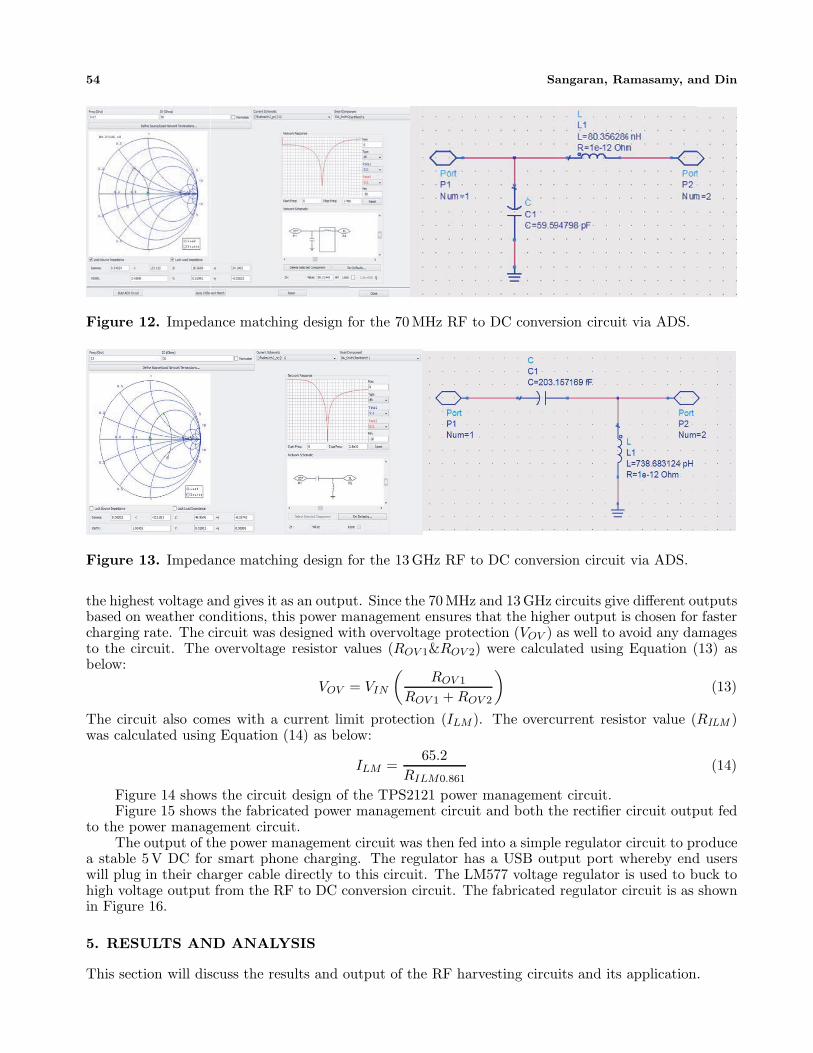
From there, the LC circuit was derived and fabricated at the input of the rectifier circuit as shown inFigure 11. Figure 12 shows the impedance matching design for the 70 MHz RF to DC conversion circuitvia ADS.
The input impedance of the 13 GHz RF to DC conversion was measured to be at 72.87−j59.94. TheADS Smith chart utility was used to match the impedance of 50 Ω to the input impedance 72.87−j59.94.Figure 13 shows the impedance matching design for the 13 GHz RF to DC conversion circuit via ADS.
With the LC impedance matching circuit, a better power transfer from the transmission path to theRF to DC conversion circuit was noticed. The results will be discussed in a greater detail in Section 5.
4.3. Power Management
The TI TPS2121 power mux IC was used to design the power management circuit by feeding both theDC voltages from the RF to DC circuits [13]. The power management circuit will select the input with
54 Sangaran, Ramasamy, and Din
Figure 12. Impedance matching design for the 70 MHz RF to DC conversion circuit via ADS.
Figure 13. Impedance matching design for the 13 GHz RF to DC conversion circuit via ADS.
the highest voltage and gives it as an output. Since the 70 MHz and 13 GHz circuits give different outputsbased on weather conditions, this power management ensures that the higher output is chosen for fastercharging rate. The circuit was designed with overvoltage protection (VOV ) as well to avoid any damagesto the circuit. The overvoltage resistor values (ROV 1&ROV 2) were calculated using Equation (13) asbelow:
VOV = VIN
(ROV 1
ROV 1 + ROV 2
)(13)
The circuit also comes with a current limit protection (ILM ). The overcurrent resistor value (RILM )was calculated using Equation (14) as below:
ILM =65.2
RILM0.861(14)
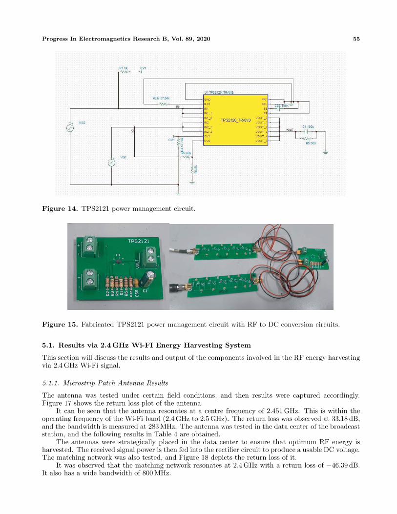
Figure 14 shows the circuit design of the TPS2121 power management circuit.Figure 15 shows the fabricated power management circuit and both the rectifier circuit output fed
to the power management circuit.The output of the power management circuit was then fed into a simple regulator circuit to produce
a stable 5V DC for smart phone charging. The regulator has a USB output port whereby end userswill plug in their charger cable directly to this circuit. The LM577 voltage regulator is used to buck tohigh voltage output from the RF to DC conversion circuit. The fabricated regulator circuit is as shownin Figure 16.
5. RESULTS AND ANALYSIS
This section will discuss the results and output of the RF harvesting circuits and its application.
Progress In Electromagnetics Research B, Vol. 89, 2020 55
Figure 14. TPS2121 power management circuit.
Figure 15. Fabricated TPS2121 power management circuit with RF to DC conversion circuits.
5.1. Results via 2.4 GHz Wi-FI Energy Harvesting System
This section will discuss the results and output of the components involved in the RF energy harvestingvia 2.4 GHz Wi-Fi signal.
5.1.1. Microstrip Patch Antenna Results
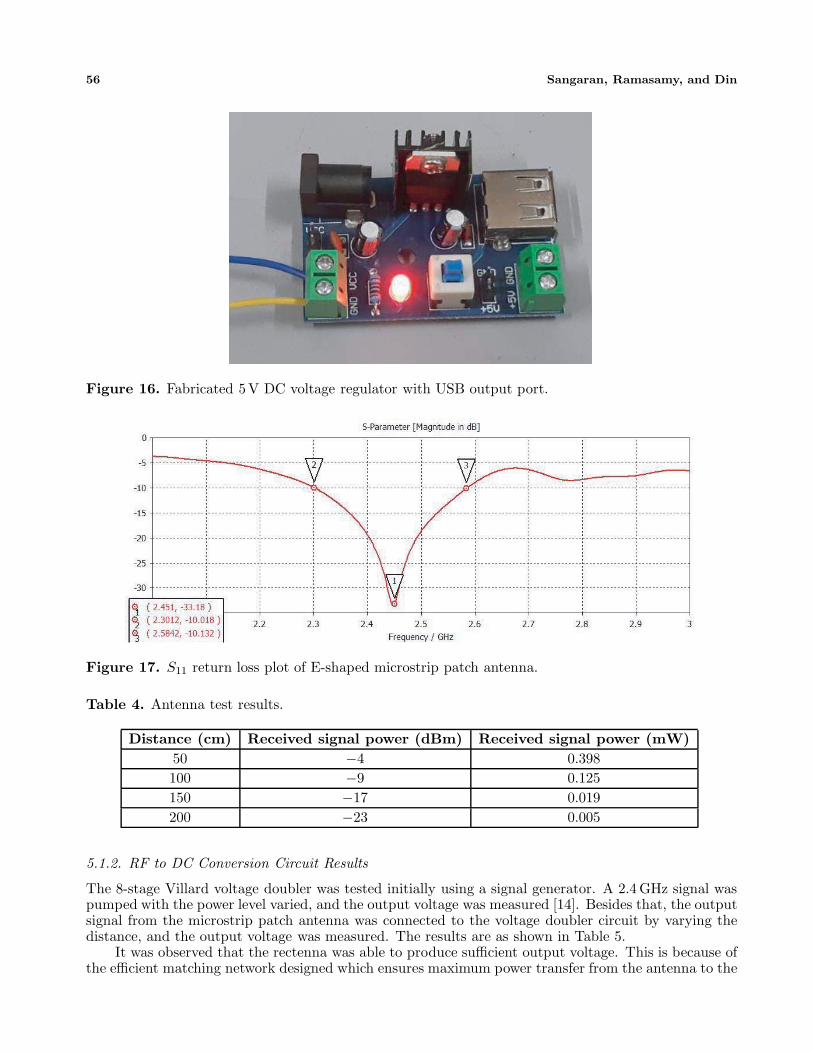
The antenna was tested under certain field conditions, and then results were captured accordingly.Figure 17 shows the return loss plot of the antenna.
It can be seen that the antenna resonates at a centre frequency of 2.451 GHz. This is within theoperating frequency of the Wi-Fi band (2.4 GHz to 2.5 GHz). The return loss was observed at 33.18 dB,and the bandwidth is measured at 283 MHz. The antenna was tested in the data center of the broadcaststation, and the following results in Table 4 are obtained.
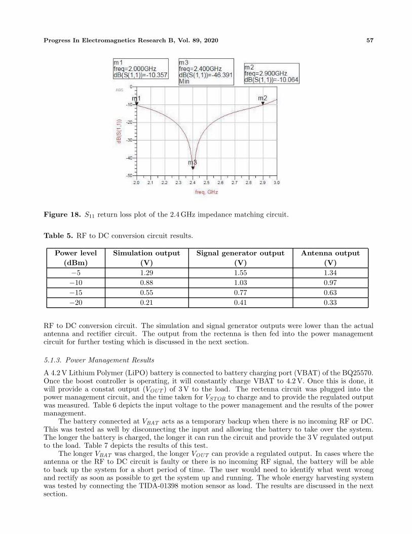
The antennas were strategically placed in the data center to ensure that optimum RF energy isharvested. The received signal power is then fed into the rectifier circuit to produce a usable DC voltage.The matching network was also tested, and Figure 18 depicts the return loss of it.
It was observed that the matching network resonates at 2.4 GHz with a return loss of −46.39 dB.It also has a wide bandwidth of 800 MHz.
56 Sangaran, Ramasamy, and Din
Figure 16. Fabricated 5V DC voltage regulator with USB output port.
Figure 17. S11 return loss plot of E-shaped microstrip patch antenna.
Table 4. Antenna test results.
Distance (cm) Received signal power (dBm) Received signal power (mW)50 −4 0.398100 −9 0.125150 −17 0.019200 −23 0.005
5.1.2. RF to DC Conversion Circuit Results
The 8-stage Villard voltage doubler was tested initially using a signal generator. A 2.4 GHz signal waspumped with the power level varied, and the output voltage was measured [14]. Besides that, the outputsignal from the microstrip patch antenna was connected to the voltage doubler circuit by varying thedistance, and the output voltage was measured. The results are as shown in Table 5.
It was observed that the rectenna was able to produce sufficient output voltage. This is because ofthe efficient matching network designed which ensures maximum power transfer from the antenna to the
Progress In Electromagnetics Research B, Vol. 89, 2020 57
Figure 18. S11 return loss plot of the 2.4 GHz impedance matching circuit.
Table 5. RF to DC conversion circuit results.
Power level(dBm)
Simulation output(V)
Signal generator output(V)
Antenna output(V)
−5 1.29 1.55 1.34−10 0.88 1.03 0.97−15 0.55 0.77 0.63−20 0.21 0.41 0.33
RF to DC conversion circuit. The simulation and signal generator outputs were lower than the actualantenna and rectifier circuit. The output from the rectenna is then fed into the power managementcircuit for further testing which is discussed in the next section.
5.1.3. Power Management Results
A 4.2 V Lithium Polymer (LiPO) battery is connected to battery charging port (VBAT) of the BQ25570.Once the boost controller is operating, it will constantly charge VBAT to 4.2 V. Once this is done, itwill provide a constat output (VOUT ) of 3V to the load. The rectenna circuit was plugged into thepower management circuit, and the time taken for VSTOR to charge and to provide the regulated outputwas measured. Table 6 depicts the input voltage to the power management and the results of the powermanagement.
The battery connected at VBAT acts as a temporary backup when there is no incoming RF or DC.This was tested as well by disconnecting the input and allowing the battery to take over the system.The longer the battery is charged, the longer it can run the circuit and provide the 3V regulated outputto the load. Table 7 depicts the results of this test.
The longer VBAT was charged, the longer VOUT can provide a regulated output. In cases where theantenna or the RF to DC circuit is faulty or there is no incoming RF signal, the battery will be ableto back up the system for a short period of time. The user would need to identify what went wrongand rectify as soon as possible to get the system up and running. The whole energy harvesting systemwas tested by connecting the TIDA-01398 motion sensor as load. The results are discussed in the nextsection.
58 Sangaran, Ramasamy, and Din
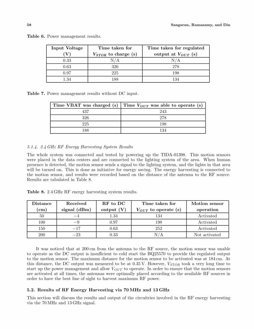
Table 6. Power management results.
Input Voltage(V)
Time taken forVSTOR to charge (s)
Time taken for regulatedoutput at VOUT (s)
0.33 N/A N/A0.63 326 2780.97 225 1981.34 188 134
Table 7. Power management results without DC input.
Time VBAT was charged (s) Time VOUT was able to operate (s)437 243326 278225 198188 134
5.1.4. 2.4GHz RF Energy Harvesting System Results
The whole system was connected and tested by powering up the TIDA-01398. This motion sensorswere placed in the data centers and are connected to the lighting system of the area. When humanpresence is detected, the motion sensor sends a signal to the lighting system, and the lights in that areawill be turned on. This is done as initiative for energy saving. The energy harvesting is connected tothe motion sensor, and results were recorded based on the distance of the antenna to the RF source.Results are tabulated in Table 8.
Table 8. 2.4 GHz RF energy harvesting system results.
Distance(cm)
Receivedsignal (dBm)
RF to DCoutput (V)
Time taken forVOUT to operate (s)
Motion sensoroperation
50 −4 1.34 134 Activated100 −9 0.97 198 Activated150 −17 0.63 252 Activated200 −23 0.33 N/A Not activated
It was noticed that at 200 cm from the antenna to the RF source, the motion sensor was unableto operate as the DC output is insufficient to cold start the BQ25570 to provide the regulated outputto the motion sensor. The maximum distance for the motion sensor to be activated was at 184 cm. Atthis distance, the DC output was measured to be at 0.35 V. However, VSTOR took a very long time tostart up the power management and allow VOUT to operate. In order to ensure that the motion sensorsare activated at all times, the antennas were optimally placed according to the available RF sources inorder to have the best line of sight to harvest maximum RF power.
5.2. Results of RF Energy Harvesting via 70 MHz and 13 GHz
This section will discuss the results and output of the circuitries involved in the RF energy harvestingvia the 70 MHz and 13 GHz signal.

Progress In Electromagnetics Research B, Vol. 89, 2020 59
5.2.1. LC Matching Network Circuits Results
As discussed earlier, two LC matching networks were designed for the 70 MHz and 13 GHz RF to DCconversion circuits. The return loss plot in Figure 19 shows the results of the matching network designedfor the 70 MHz and 13 GHz circuits, respectively.
Figure 19. Return loss plots for 70 MHz and 13 GHz LC matching network circuits.
For the 70 MHz circuit, the return loss was recorded at −64.768 dB, and the bandwidth is at40 MHz. For the 13 GHz circuit, the return loss was measured at −46.933 dB, and the bandwidth isat 4GHz. The rectifier circuit was tested with and without the LC matching network circuit, and theoutput seemed to be improved with the matching network. The results of this are discussed in the nextsection.
5.2.2. RF to DC Conversion Circuit Results
The RF to DC conversion circuit was initially tested with a signal generator by pumping in 70 MHz and13 GHz signals. Power levels were varied in order to test the performance of the circuit. The circuitswere tested with and without matching networks. Table 9 shows the results of the 70 MHz and 13 GHzRF to DC conversion circuit.
The results show that the RF to DC conversion circuit had better efficiency with the LC matchingnetwork circuit as the loss is minimal due impedance matching and allows proper power transfer. At
Table 9. 70 MHz & 13 GHz RF to DC conversion circuit results.
Powerlevel (dBm)
DC output withoutmatching network (V)
DC output withmatching network (V)
70 MHz 13 GHz 70 MHz 13 GHz−5 3.4 0 5.2 00 5.8 0 7.6 05 8.7 0 10.2 010 12.4 2.3 18.2 3.620 N/A 8.7 N/A 13.430 N/A 19.8 N/A 23.1

60 Sangaran, Ramasamy, and Din
+10 dBm, the 70 MHz circuit produces a DC output of 18.2 V. The circuit was not further tested withhigher power levels as the diodes maximum input power level is at +10 dBm. At lower power levels,the 13 GHz circuitry was unable to produce any DC output as it suffers major loss due to the highfrequency. At +30dBm, the 13 GHz circuit produced a DC output of 23.1 V. This DC outputs are fedinto the power management circuit and finally regulated to 5 V. Sufficient amount of current is producedfor smart phone charging when these high voltage outputs are stepped down to 5V at the final stage.
5.2.3. Power Management Circuit Results
The TPS2121 power management circuit switches to higher power supply seamlessly, and this wasinitially tested using a DC power supply. Later, the RF to DC conversion circuit was connected to theTPS2121 circuit and was tested. The first input (V 1) of the TPS2121 was connected to the 70 MHzcircuit, and the second input (V 2) was connected to the 13 GHz input.
The overvoltage protection of the first input was designed to be at 18 V, and the second inputovervoltage was at 24 V as reference to the results of the RF to DC circuits at +10 dBm for the 70 MHzcircuit and +30 dBm for the 13 GHz circuit. The circuit was tested by connecting to a DC power supply,and the overvoltage protection was noticed working fine. Both the 70 MHz and 13 GHz circuits werethen connected to the TPS2121 circuit as shown in Figure 20.
Figure 20. 70 MHz and 13 GHz RF to DC conversion circuits connected to TPS212.
The power management circuit was tested by varying the power level to the input of the RF to DCcircuits. This is done by using the signal generator. The results are tabulated in Table 10.
It was noticed that initially V 1 is the active output as the voltage is higher than V 2. Once the
Table 10. Power management results.
Power level (dBm) DC output (V) Active output70 MHz (V 1) 13 GHz (V 2)
−5 5.2 0 V 10 7.6 0 V 15 10.2 0 V 110 18.2 3.6 V 120 N/A 13.4 V 130 N/A 23.1 V 2

Progress In Electromagnetics Research B, Vol. 89, 2020 61
voltage on V 2 rises, the circuit automatically switches to V 2 and outputs it to the load. Once V 2decreases, the circuit automatically switches back to V 1 and maintains at it until a rise is noticed onV 2. The RF to DC circuit was then connected to the uplink transmission path, and the same wasobserved. During clear sky operations, the 70 MHz RF to DC output is used to power up the load.When it rains, the 13 GHz RF to DC output is higher, and the power management selects this voltageinstead to power up the load.
5.2.4. RF Energy Harvesting via 70MHz and 13GHz Results
The RF to DC conversion circuits were connected to the TPS2121 power management circuit. Theoutput of the TPS2121 was connected to the voltage regulator. A smart phone was plugged to the USBoutput of the voltage regulator circuit. For testing purposes, the Samsung Galaxy A8 phone was usedto test the charging rate. This phone has fast charging capability, and the nominal current required forthis is 2 A. However, the RF energy harvesting circuit will not be able to produce such high currents,hence a slow but acceptable charging rate is expected. The system was tested, and the results aretabulated in Table 11.
Table 11. RF energy harvesting via 70 MHz and 13 GHz results.
InputDC output
(V)Regulated DC
output (V)Current
(A)Time taken to
fully charge (min)70 MHz at +10 dBm 18.2 5 0.3 12313 GHz at +30 dBm 23.1 5 0.5 84
From the results measured, it can be seen that the 13 GHz circuit provides a better current outputand in return has a faster charging rate than the 70 MHz circuit. The current is approximately 0.5 Awhich is the same as any USB charging port available on laptops, TV, or any other devices. The timetaken to fully charge the handphone is quite high compared to a normal charger as the current is lower,and in return a slower charging rate is expected.
Users can temporarily use this charging facility in case of emergency or for backup if they havemisplaced their charger. This is somehow a form of renewable energy available 24 × 7 whereby unusedcoupler outputs of RF energy are converted into usable DC power which is used for smart phonecharging. Especially during this era where smart phones are an essential, this charging facility willdefinitely benefit the end users.
6. CONCLUSION
In conclusion, two types of RF energy harvesting systems are designed and implemented in a broadcaststation. First is the 2.4 GHz energy harvesting system placed in the data center which is used to powerup motion sensors connected to the lighting system in the area. An E-shaped microstrip path antenna isplaced 185 cm away from its source, producing a DC voltage of 0.35 V, which is sufficient to start up theBQ25570 power management circuit. The BQ25570 then provides a constant 3V regulated output topower up the TIDA-01398 motion sensor and charges a 4.2 V LiPO rechargeable battery simultaneously.In case there is no incoming RF or DC, the battery can be used as a temporary backup to power upthe system.
The second energy harvesting system consists of the 70 MHz signal from the modulator and 13 GHzfrom the high-power amplifier derived from the uplink system. LC matching networks were designed,and the DC outputs were connected to the TPS2121 power management circuit which selects the higherDC input. During normal operation, the 70 MHz is expected to charge the smart phone at chargingrate of 0.3 A. During rain, the high-power amplifier will have a higher output, and the 13 GHz circuitis expected to charge the smart phone at a charging rate of 0.5 A. Compared to other studies, thiswork has excelled in harvesting from high frequency and also to use the converted DC for smart phonecharging instead of other low power application. Increasing the charging rate is something to be lookedinto for future researches.

62 Sangaran, Ramasamy, and Din
ACKNOWLEDGMENT
This work is supported by the Ministry of Science, Technology and Innovation Malaysia (No. 03-0203-SF0291) and also by Universiti Tenaga Nasional BOLD Publication Fund code numberRJO10436494/iRMC/Publication/2020.
REFERENCES
1. Diagarajan, M. S., A. Ramasamy, N. B. M. Din, and P. N. Vummadisetty, “A review on thecontemporary research on radio frequency energy harvesting,” International Journal of Engineeringand Technology (UAE), Vol. 7, No. 3, 52–58, 2018.
2. Alneyadi, F, M. Alkaabi, S. Alketbi, S. Hajraf, and R. Ramzan, “2.4 GHz WLAN RF energyharvester for passive indoor sensor nodes,” Proc. 2014 IEEE International Conference onSemiconductor Electronics (ICSE), 471–474, Aug. 27–29, 2014.
3. Mikeka, C. and H. Arai, “Design issues in radio frequency energy harvesting system,” SustainableEnergy Harvesting Technologies — Past, Present and Future, Dec. 2011.
4. Pinuela, M., P. D. Mitcheson, and S. Lucyszyn, “Ambient RF energy harvesting in urban and semi-urban environments,” IEEE Transactions on Microwave Theory and Techniques, Vol. 61, No. 7,2715–2726, Jul. 2013.
5. Diagarajan, M. S., A. Ramasamy, N. Boopalan, and N. B. M. Din, “RF energy harvesting prototypeoperating on multiple frequency bands with advanced power management,” Indonesian Journal ofElectrical Engineering and Computer Science, Vol. 17, No. 1, 70–77, 2019.
6. Adami, S.-E., C. Vollaire, B. Allard, F. Costa, W. Haboubi, and L. Cirio, “Ultra-low powerautonomous power management system with effective impedance matching for RF energyharvesting,” 2014 8th International Conference on Proc. Integrated Power Systems (CIPS), 1–6,Feb. 25–27, 2014.
7. Diagarajan, M., A. Ramasamy, N. M. Din, and K. K. A. Devi, “Comparison on microstrip patchantenna modules and rectifier modules for RF energy harvesting,” ARPN Journal of Engineeringand Applied Sciences, Vol. 11, No. 10, 6228–6233, 2016.
8. Yi, J., W. Ki, and C. Tsui, “Analysis and design strategy of UHF micro-power CMOS rectifiersfor micro-sensor and RFID applications,” IEEE Trans. Circuits Syst., Vol. 54, No. 1, 153–166,Jan. 2007.
9. Kong, N. and D. S. Ha, “Low-power design of a self-powered piezoelectric energy harvesting systemwith maximum power point tracking,” IEEE Transactions on Power Electronics, Vol. 27, No. 5,2298–2308, May 2012.
10. Sedeek, A., E. Tammam, and E. Hasaneen, “High efficiency 2.45 GHz low power hybrid junctionrectifier for RF energy harvesting,” 2018 International Japan-Africa Conference on Electronics,Communications and Computations (JAC-ECC), 147–150, Alexandria, Egypt, 2018.
11. Pulvirenti, F., A. La Scala, D. Ragonese, K. D’Souza, G. M. Tina, and S. Pennisi, “4-phase interleaved boost converter with IC controller for distributed photovoltaic systems,” IEEETransactions on Circuits and Systems I: Regular Papers, Vol. 60, No. 11, 3090–3102, Nov. 2013.
12. Devi, K. K. A., M. D. Norashidah, C. K. Chakrabarty, and S. Sadasivam, “Design of an RF-DCconversion circuit for energy harvesting,” Proc. 2012 IEEE International Conference on ElectronicsDesign, Systems and Applications (ICEDSA), 156–161, Kuala Lumpure, Nov. 5-6, 2012.
13. Diagarajan, M., A. Ramasamy, N. M. Din, and K. K. A. Devi, “Comparison on microstrip patchantenna modules and rectifier modules for rf energy harvesting,” ARPN Journal of Engineeringand Applied Sciences, Vol. 11, No. 10, 6228–6233, 2016.
14. Sedeek, A., E. Tammam, and E. Hasaneen, “High efficiency 2.45 GHz low power hybrid junctionrectifier for RF energy harvesting,” 2018 International Japan-Africa Conference on Electronics,Communications and Computations (JAC-ECC), 147–150, Alexandria, Egypt, 2018.