adhesion of polymers to tungsten as studied by field ion
TRANSCRIPT

NASA TECHNICAL NOTE k * N L n
*f)n
ADHESION OF POLYMERS TO TUNGSTEN AS STUDIED BY FIELD ION MICROSCOPY
by William A. Bruinurd und Dondld H. Bivckley
Lewis Research Center
N A T I O N A L AERONAUTICS A N D SPACE A D M I N I S T R A T I O N W A S H I N G T O N , D. C. OCTOBER 1971 i 1 !
1

--
TECH LIBRARY KAFB, NM
I1111111111111111I l l11#1 IllIIIIIIll1Ill 0333432-
1. Report No. 1 2. Government Accession No. I 3. Recipient's Catalog No.
. NASA TN D-6524 I I 4. Title and Subtitle 5. Report Date
ADHESION OF POLYMERS TO TUNGSTEN AS STUDIED October 1971
BY FIELD ION MICROSCOPY I 6. Performing Organization Code
7. Author(s) 8. Performing Organization Report No. William A. B r ainard and Donald H. Buckley I E-6471
10. Work Unit No. 9. Performing Organization Name and Address 114-03
Lewis Research Center 11. Contract or Grant No.
National Aeronautics and Space Administration Cleveland, Ohio 44 135
13. Type of Report and Period Covered '2. Sponsoring Agency Name and Address Technical Note
National Aeronautics and Space Administration 14. Sponsoring Agency Code
Washington, D. C. 20546 I
5. Supplementary Notes
- -. . . ~~
6. Abstract
Mechanical contacts with polytetrafluoroethylene (PTFE) and polyimide polymer (PI) contacting tungsten field ion microscope emit ter t ips were conducted in vacuum. The metal polymer interface w a s examined on an atomic scale by helium field ion microscopy. Mechanical t ransfer was observed upon simple touch contact of the polymer mater ia ls to tungsten. The t ransferred polymers were stable even a t the high field necessary for helium ionization, thus implying a strong chemical bonding to the metal surface. The mechanical contact s t r e s s e s orient the t ransferred mater ia l on the tungsten surface in a radial manner from the center of contact. With sufficient load the P T F E and PI cause deformation of the tungsten. On the tungsten (110) plane, individual molecular c lus te rs can be resolved.
7. Key Words (Suggested by Author(s) ) 18. Distribution Statement Adhesion, Polymer, Polytetrafluoroethylene, Unclassified - unlimited Polyimide, Tungsten, Field ion microscope
. .
9. Security Classif. (of this report) 20. Security Classif. (of this page) 21. No. of Pages 22. Price' Unclassified Unclassified 32 $3.00
* For sale by the National Technical Information Service, Springfield, Virginia 22151

ADHESION OF POLYMERS TO TUNGSTEN AS
STUDIED BY FIELD ION MICROSCOPY
by Wil l iam A. Bra inard and Donald H. Buckley
Lewis Research Center
SUMMARY
Organic polymers a r e used extensively in lubrication systems. Fundamental to using these materials as lubricants is adherence between the polymers and metal surfaces. In this investigation, experiments were conducted using the field ion microscope (FIM) to study and characterize the polymer-metal interface on an atomic scale. Mechanical contact between the polymeric material polytetrafluoroethylene (PTFE) and polyimide polymer (PI) with the clean tungsten field ion emitter tip were made in si tu in the FIM. Both the PTFE and PI t ransferred to the tungsten metal t ip on simple mechanical touch contact. Furthermore, the images of the transferred material were stable with helium ion imaging. Thus, the t ransferred polymers were very strongly bonded which implies chemical bonding (i.e. , the formation of an organometallic bond).
Furthermore, the transferred polymeric fragments were oriented on the tungsten surface in a manner suggesting they were alined by the contact s t r e s s radially outward from the center of the contact zone. With heavier loads both the PTFE and PI caused deformation of the tungsten tip. On the (110) plane, certain individual polymer molecular clusters could be resolved, in particular. Some PTFE fragments a r e observable which resemble the PTFE structure and which may represent a single monomer of the polymer chain.
INTRODUCTlON
In a lubrication system, the relative motion of the components gives r i s e to friction and wear. The friction and wear properties of materials in sliding contact can be related to the behavior of the materials at the sliding interface. With metals in sliding contact, adhesion at the interface is the significant factor in the friction and wear process. To reduce the friction and wear a lubricant is used. For many applications conventional

lubricants such as oils and greases cannot be used. In these cases solid lubricant materials, both inorganic and organic, often are used.
A common organic solid lubricant material is polytetrafhoroethylene (PTFE). PTFE has been studied under vacuum conditions with sliding friction experiments and as a component in bearing systems (refs. 1 and 2). The very stable polyimide polymer (PI) materials have also been studied (ref. 3) and are employed as cage materials for bearings.
Fundamental to using these materials is their adherence to the sliding surface. The adherence of the material during application and subsequently during running determines to a large extent its ability to function as a lubricant. Thus, a fundamental understanding of the adherence of a solid lubricant to metal surfaces will significantly aid in the selection and application of potential lubricant materials.
Previous work has shown that the field ion microscope is a powerful tool for fundamental studies of the adhesion and surface characterization of metal-metal contacts (refs. 4 and 5). The purpose of this investigation was to determine i f the field ion microscope could be used to study the polymer-metal interface and, i f so, t o characterize the interaction of the lubricant with the metal surface.
To accomplish this objective experiments were conducted in which mechanical contacts were made with solid lubricant materials contacting the field ion microscope emitt e r tip. The contacts were made in s i tu in the field ion microscope vacuum system. The solid lubricant materials examined in contact with tungsten on the metal emitter t ip were polytetrafluoroethylene (PTFE) and polyimide polymer (PI).
A P PARATUS
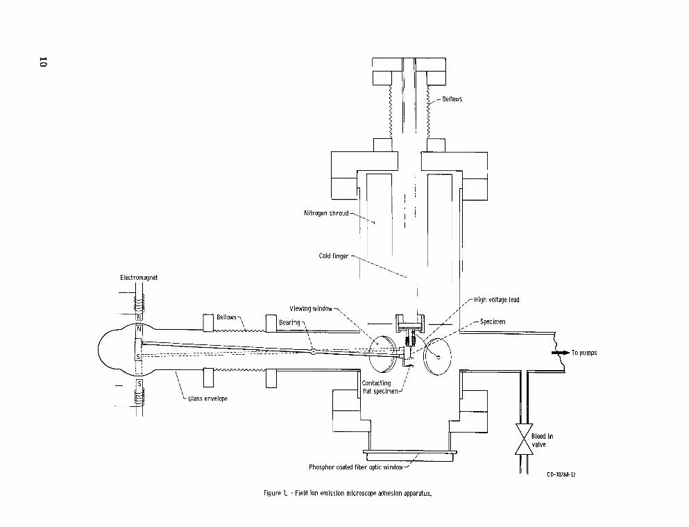
Field Ion Microscope (FIM)
The field ion microscope is shown schematically in figure 1. The microscope is of metal construction with copper sealing gaskets so the system can be baked out to achieve low background pressures. The field emitter is mounted by tack welding to a nickel wire loop which slips over two copper posts extending down from the end of the cryogenically cooled cold finger. Also attached to the copper posts is the high voltage (0 to 30 kV) lead. The copper post mounting disk is separated from the metal (ground) end of the cold finger by sapphire disks which se rve both as electrical insulators and thermal conductors. The cold finger is cooled by either filling it with liquid nitrogen (78 K ) , liquid helium (4.2 K ) , or by using a two-stage commercial cryostat which can be inserted down the cold finger tube to liquify hydrogen ( 2 1 K ) . The cold finger is welded to a flange which mates with a bellows assembly used to vary the vertical position of the tip. Tip to screen distance can be varied from 8 t o 5 centimeters by bellows compression.
2
I

The screen of the FIM is a tin oxide coated fiber optic window 7 .6 centimeters in diameter with an average fiber diameter of 16 microns. Phosphor is coated on the inside of the fiber optic screen by using an ar t is t ' s air brush. Photography of the field ion image is done by direct contact photography methods. The film is pressed against the outside of the fiber optic window, and this essentially uses the fiber bundles to transmit the image from inside the screen t o the emulsion.
The image gas system consisted simply of cylinders of research grade helium and neon which were bled into the evacuated microscope to a pressure around 3 millitorr with a variable leak valve.
The vacuum system of the field ion microscope consisted of a cryosorption fore pump, a 20/400 l i ter per second combination ion pump and water cooled titanium getter pump, and a noble gas pumping 50 l i ter per second ion pump. Chamber pressure was monitored at imaging pressure by a thermocouple gage and at UHV conditions with a triggered discharge gage. With moderate bakeout (250' C), chamber pressure was 1 0 - ~ O t o r r .
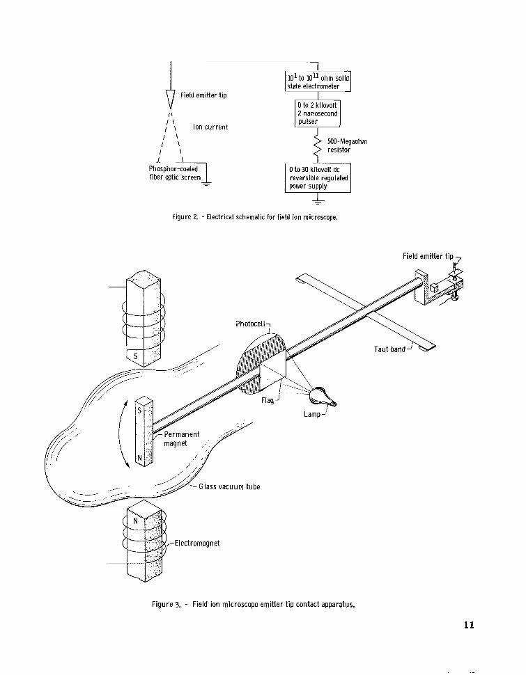
The electrical schematic of the FIM is shown in figure 2. A regulated, reversible, 0 to 30 kilovolt dc power supply is used in the positive mode for field ionization. A 2nanosecond pulser with variable pulse height from 0 to 2 kilovolts is floated at the 30kilovolt supply bias level. The pulser is capable of single manual pulsing o r repetitive pulsing at 60 cycles per second. The pulser permits controlled field evaporation of the specimen at ra tes from 1atomic layer to several layers per second. Between the HV supply and the pulser is a 500-megohm resis tor for preventing damaging electrical breakdowns inside the microscope. Also floated in ser ies is a solid s ta te electrometer for measuring the ion and emission current. The electrometer is protected against breakdown by an input to chassis diode couple (27-v breakdown voltage).
Emitter Contactor Apparatus
The manipulator which was used for contacting the field ion emitter t ip is shown schematically in figure 3. Basically the device is a stainless steel beam mounted on a taut band. On one end of the beam is a small permanent bar magnet. Above and below the ba r magnet, outside the glass vacuum tube, a r e two small electromagnets wired so that like poles face the permanent magnet. The beam can be made to move either up or down by varying current to the electromagnets. On the other end of the beam is a platform which by the compression of the horizontal bellows, is moved under the field emitte r tip f o r contact. On the platform is the material with which the tip is touched.
Also mounted on the beam is a stainless s teel flag which acts to intercept the light f rom a small lamp to a photocell. The shadow cast on the photocell changes the resistance of the cell, which causes a change in voltage to the electromagnets. This
3

photocell-electromagnet voltage system serves to damp out vibrations. The photocell voltage also se rves as a monitor for beam position. Photocell voltage is amplified and read on a multirange recorder . Any change in beam position is reflected in photocell voltage which is recorded.
The contact of the t ip was sensed by using the defection of a thin spring. In this ca se a foil of platinum was welded to a linear spring. When contact with the field t ip occurs, the spring deflects enough s o the foil makes an electrical contact with an electrode just below the foil. The spring and foil a r e grounded, thus causing a measurable current between the electrode and ground which is read on a meter outside the microscope. The gap between the foil and the electrode can b e set to vary the force required to give a current indication. The gap spacing could be set close enough s o that loads less than 0.25 milligram could b e sensed. Even this small load is sufficient to produce a high contact s t r e s s .
Precalibration of contact force as a function of electromagnet current is accomplished by using an electronic balance with a sensitivity of 0.01 milligram. A known load can b e applied to the contacted t ip by applying more electromagnet current to the top magnet. After contacting and loading is completed, the current to the top electromagnet is reduced until the t ip and contact material separate.
To reduce the influence of ambient vibrations on the experiments, the entire field ion microscope including pumps, power supplies, gages, gas supply systems, e tc . , and the emitter contactor apparatus a r e mounted on a vibration isolation table. The vibration table uses air piston suspension and has a natural frequency of 1.1hertz with better than 90 percent isolation at resonant frequencies of 7 to 20 hertz.
PROCEDURE
The t ip contact procedure is shown as a flow diagram in figure 4 . The t ip is electroetched from fine high purity wire to an extremely fine radius (<500 A ) . Methods for t ip preparation a r e discussed in the l i terature (ref. 6). Following etching, the specimen is mounted on the cold finger and the FIM is pumped into the UHV range.
The t ip is imaged at a pressure around 3 milli torr with either helium or neon gas. Field evaporation is conducted to increase t ip radius and to prepare a nearly perfect crystallographic surface. After field evaporation, the image gas is pumped out while the high voltage is kept on to prevent contamination of the tip. After pressure is less than lo” t o r r , the high voltage is turned off. A clean surface can be maintained for several minutes at pressures below lo-’ t o r r .
Following the pump down, the emitter contact apparatus is moved under the t ip by bellows compression. The platform is then raised until the t ip contacts the solid lubricant material as sensed by the electrode contacting the metallized underside of the
4

lubricant material. At this point additional loading may be applied beyond that required t o close the preset gap (0.25 mg). The load is then removed and the image of the surface reestablished by readmitting the image gas and turning on the high voltage. The sterographic projection of the body centered cubic lattice is shown in figure 5.
RESULTS
Polytetrafluoroethylene - Tungsten
Mechanical contacts of tungsten emitter tips by PTFE were made in vacuum of 10-10
torr . Figure 6 shows the precontact image of a somewhat imperfect tip. The dark a r e a is a furrow between two protruding asperities. Figure 7 is the same t ip after being contacted with PTFE. The surface is characterized by a random appearance containing many bright spots. Note the diffuse tails extending outward from many of the spots. These diffuse tails a r e more evident in figure 8 which was taken at a slightly higher voltage. There a r e apparent molecular structures which can be resolved on the (110) plane. It is likely that many of the other bright spots a r e more than one atom but cannot b e r e solved because of their enhanced brightness. These apparent molecular structures have an appearance very s imilar to the end view of a PTFE chain. Structural illustrations of the PTFE chain and of the PI s t ructure are shown in figure 9. It is thus believed that some PTFE has t ransferred to the tungsten surface and that the molecular images r e solved on (110) plane represent a fragment of a PTFE chain, possibly a single monomer. Furthermore, the bonding is strong enough to withstand the helium image field without desorbing. This strong bonding suggests a tungsten-carbon bond formed at the interface. Figure 10 is a micrograph of the same surface taken at 18.0 kilovolts. Several of the bright spots that appeared in figures 7 and 8 have now desorbed. In addition, the remaining ones do not exhibit the diffuse tails that were observed previously. It is not clear what causes these tails. During metal-metal contact, reference 5, there was no evidence of diffuse tails as was observed with the PTFE. It is of interest to note that the tails appear to be projected outward from a point near the bottom of the micrograph. This point may represent the center of the mechanical contact and the tail-like s t ructure may be due to an orientation effect caused by the s t r e s ses exerted radially from the cent e r of the contact.
Figure 11is a micrograph taken at 17.5 kilovolts after raising the voltage to 19.0 kilovolts. Some further desorption has occurred, but generally the image is similar t o that of f igure 10. The micrograph in figure 12 was taken after raising the voltage t o 22.0 kilovolts in order to desorb the PTFE from the (110) plane.
Repeating the experiments with lightly loaded tungsten-PTFE contacts showed s imilar results .
5

A heavily loaded tungsten-PTFE (approximately three t imes more load) contact gave the rather surprising result that extensive deformation of the tungsten occurred. Figu r e 13 shows the precontact micrograph, and figure 14 shows a postcontact micrograph. This photograph was taken after the desorption of the adhered PTFE. The deformation extended far into the bulk of the material as shown in figure 15, which was taken after extensive field evaporation (an effective increase in t ip radius of approximately fifty per -cent). Generally, during heavy loaded contacts the t ip will bend so that the image is often displaced on the screen; however, there is no displacement of (110) in these micrographs. The t ip, when pressed into the PTFE, may be prevented from bending and thus absorbing the s t r e s s further up the shank by the very large a rea of contact (relative to metal -metal contacts).
Polyimide - Tungsten
Mechanical contacts with a polyimide polymer (PI) contacting tungsten tips were made in vacuum of lo-’ t o r r with both light and heavy loads. Figure 16 is a precontact micrograph of tungsten. This particular t ip had been contacted previously as there is some deformation in the vicinity of the (100) plane. Figure 17 shows a micrograph after the light load PI contact. The surface is again characterized by a random distribution of bright spots. Figure 18 is the same tip with an increase of 500 volts during imaging. Many of the spots in figures 17 and 18 a r e elongated and appear to contain groups of atoms as if they were transferred molecular fragments of PI. Figure 19 is a micrograph taken at 14.5 kilovolts. Considerable desorption has occurred and the underlying tungsten is visible. Note the surface has not been displaced nor is there any obvious evidence of further deformation. As with PTFE, the (110) plane appears to have several polymer fragments adhered to it. Figure 20, taken at 15.0 kilovolts, shows further desorption has occurred, particularly on (110). It is of interest to note the change in the character of the remaining spots on (110) as the neighboring fragments desorb. Additional increases in voltage cause further desorption; however , it was necessary to evaporate the tungsten substrate to return the surface to the ordered tungsten appearance.
To determine if load would significantly influence the PI-tungsten contacts, an experiment was conducted with PI contacting tungsten using a load approximately three t imes greater than that used for light load contents. Figure 21 is the precontact micrograph. Figure 22 is the image of the same tungsten t ip after a heavily loaded PI contact. The results show a ser ies of elongated spots all radially projected outward from a dark nonimaging a r e a on the right side of the micrograph. As with PTFE, it appears that the polyimide polymer fragments have been oriented by the radial s t resses projecting outward from the center of contact, where the center of contact is the dark region t o the right in the micrograph. Figure 23 is a micrograph taken with a slightly higher voltage.
6

It can be seen that the (110) plane has been displaced to the upper left indicating the t ip is slightly bent by the force of the contact. Raising the voltage to 10.25 kilovolts caused considerable desorption of the s t reak to occur; this condition resulted in a surface that had an appearance very similar t o the light load PI contact of figure 17.
Subsequent micrographs taken with increased voltage show similar resul ts to those light load PI-tungsten contact micrographs.
D ISCUSS ION
The resul ts of this study with PTFE and PI polymers in contact with tungsten indicate that polymers will t ransfer to a clean metal surface on simple touch contact and that the bond formed reflects more than simple mechanical transfer. The stability of the transferred polymers at the high field for helium ion imaging imply that the bond of the polymer to the metal surface is chemical in nature. With PTFE it is hypothesized that the bonding is that of carbon to the metal surface because the carbon to carbon bond is the weakest bond in the PTFE structure and the one most frequently seen broken on polymer scission (ref. 7). Furthermore, the carbon could readily interact with the clean tungsten to form bonds stable a t the imaging and field evaporation voltages applied in this study.
With the polyimide (PI) both oxygen and carbon bonding to the tungsten surface a r e possible. But again because of the imaging and evaporation voltages employed the bond must be chemical in nature.
The concept of chemical bonding of the polymers to the clean metal surface necessitates the breaking of bonds in the organic molecule and the subsequent formation of metal to carbon o r oxygen bonds to form organometallics. The breaking of organic bonds by metal surfaces is observed with hydrocarbons contacting metals in the field of catalysis. The tendency for such reactions should b e increased when the metal surface is atomically clean because of the enhanced surface activity of the metal.
The effect of loading in the t ransfer of the polyimide to the tungsten surface indicates an increased amount of polymer transfer with an increase in load. The polymer appears to remain on the tungsten surface in longer chain fragments indicating that fracture occurred deeper in the polymer body than was observed at light loads. When field evaporation was conducted the polymer chain length adhered t o the tungsten could be reduced t o that observed with light loads.
It is of interest also to note in figures 22 and 23 that preferred orientation of the polymer chains toward the zone of contact has occurred. This in all probability resulted when the tungsten was pressed into the polymer under load. Adhesion of polymer occurred to the tungsten surface. Polymer bonds were broken in the bulk and the relative tangential motion of the polymer body along the radius of the tungsten t i p resulted in texturing.
7
With heavy loading of the polymers against the tungsten surface, field evaporation of the polymer revealed a plastically deformed tungsten surface. This is believed to be the first experimental evidence for the plastic deformation of a metal surface when pressed into contact with a polymer. Tungsten has the highest cohesive energy and one of the highest elastic moduli of the metallic elements in the periodic table. Therefore, it is reasonable to assume that other metals could also be plastically deformed in their s u r ficial layers by contact with these polymers with sufficient loads.
SUMMARY OF RESULTS
Mechanical contacts of tungsten FIM emitter tips by polytetrafluoroethylene (PTFE) and polyimide polymer (PI) were conducted in the field ion microscope, and the effects of these contacts were examined on an atomic scale by field ion microscopy. The following results were obtained:
1. Both the PTFE and PI transfer to a clean tungsten surface on simple touch contact.
2. The stability of the transferred polymeric material at the high fields employed for helium field ion microscopy imply very strong chemical bonding between the polymer and the metal surface. For PTFE this suggests a tungsten-carbon bond, while for PI the bonding could possibly be either that of tungsten to oxygen o r carbon.
3. The transferred polymeric materials are oriented by the mechanical contact s t r e s s in a radial manner outward from the centers of the contact zones.
4. With sufficient load, both the PI and PTFE can cause deformation of the tungsten substrate.
5. Individual polymer molecular clusters can be resolved on the (110) plane of tungsten.
Lewis Research Center, National Aeronautics and Space Administration,
Cleveland, Ohio, July 29, 1971, 114-03.
REFERENCES
1. Buckley, D. H. ; and Johnson, R. L. : Degradation of Polymeric Compositions in Vacuum to lo-’ mm Hg in Evaporation and Sliding Friction Experiments. SPE Trans . , vol. 4, no. 4, Oct. 1964, pp. 306-314.
8

2. Steijn, R. P. : Friction and Wear of Plastics. ASM Metals Eng. Quart., vol. 7, no. 2, May 1967, pp. 9-21.
3. Buckley, Donald H. : Friction and Wear Characteristics of Polyimide and Filled Polyimide Compositions in Vacuum (10-l' mm Hg). NASA TN D-3261, 1966.
4. MGller, E. W. ; and Nisikawa, 0. : Atomic Surface Structures of the Common Transition Metals and the Effect of Adhesion as Seen by Field Ion Microscopy. Adhesion or Cold Welding of Materials in Space Environments. Spec. Tech. Publ. 431, ASTM, 1967, pp. 67-87.
5. Brainard, W. A. ; and Buckley, D. H. : Preliminary Studies by Field Ion Microscopy of Adhesion of Platinum and Gold to Tungsten and Tridium. NASA TN D-6492, 1971.
6. Mcller , Erwin W. ; and Tsong, T. T. : Field Ion Microscopy; Principles and Applications. American Elsevier Publ. Co., 1969.
7. Pauling, Linus C. : The Nature of the Chemical Bond and the Structure of Molecules and Crystals. Third ed. , Cornel1 Univ. Press, 1960, p. 85.
9
c. 0
Electromagnet
I I,,,,rHigh voltage lead
Viewins window 7
,-Specimen ,
To pumps
Contacting ,' \LGlass envelope
U flat specimen'
Avalve
I I I
Phosphor coated fiber optic window-' I' '1 CD-10784-17
Figure 1. - Field ion emission microscope adhesion apparatus.
-Field emitter t ip
I \
I I \\ Ion current I \
I \ I \
fiber optic screen
2 nanosecond
500-Megaohm resistor
0 to 30 kilovolt dc reversible regulated
Figure 2. - Electrical schematic for field ion microscope.
Field emi t ter t i p
Photocell:
Taut b a n d ’\
-’///-Glass vacuum tube
F igure 3. - Field ion microscope emi t ter t i p contact apparatus.

with voltage on to
metal contact I
potential to t ip
Move contactorLLLJ emission current
[ is 5x10⁻⁹' a m p s 1
&; II proceed yith c o n t a d
Image t ip and observe extend
interior damage
For metal nonconductor contact
close to t ip by visual observation
Move contactor toward t ip at extremely slow rate
load - unload
Figure 4. - Flow diagram of FIM t ip contact procedure.
12

13
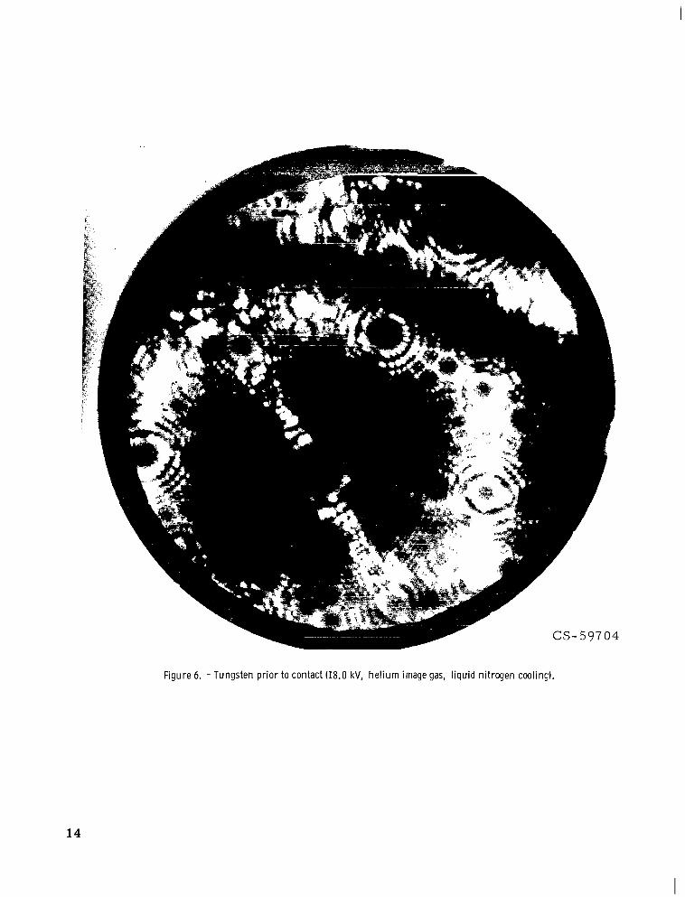
Figure 6. - T u n g s t e n p r i o r t o contact (18.0 kV, h e l i u m image gas, l i qu id n i t ragen cooling).
14

Figure 7. -Tungsten after PTFE contact (16.2 kV, hel ium image gas, liquid hel ium cooling).
15
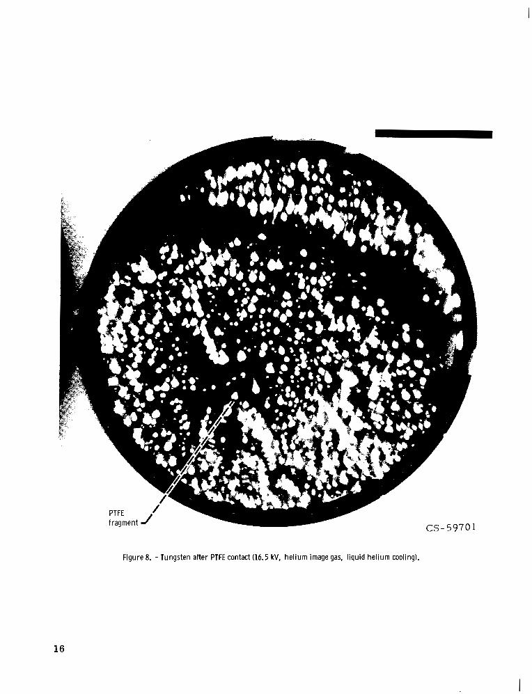
Figure 8. -Tungsten after PTFE contact (16.5 kV, h e l i u m image gas, l iqu id h e l i u m cooling).
16

17

Figure 10. - Tungsten afler PTFE contact (18.0 kV, hel ium image gas, liquid hel ium cooling).
18

1'
c
Figure 11. -Tungsten after PTFE contact (17.5 kV, hel ium image gas, takenafter raising voltage to 19.0 kV, liquid hel ium cooling).
19

Figure 12. -Tungs ten after PTFE contact (17.5 kV, h e l i u m image gas, taken after ra is ing voltage to 22.0 kV, l iqu id he l i um cooling).
20
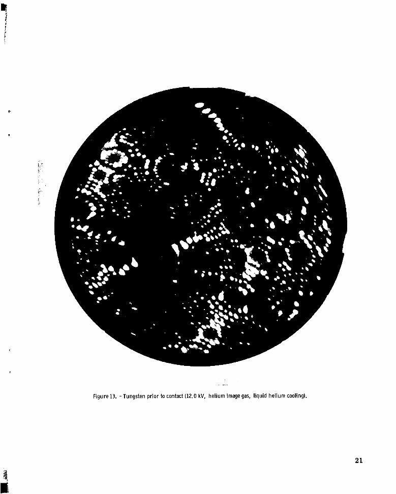
Figure 13. -Tungsten p r io r t o contact (12.0 kV, h e l i u m image gas, l iqu id h e l i u m cooling).
21

CS- 597 0 3
Figure 14. - Tungsten after heavy load PTFE contact.
22

Figure 15. -Tungsten af ter heavy load PTFE contact (20.0kV), h e l i u m image gas, after ra is ing voltage to 24.0 kV, l iqu id h e l i u m cooling).
23

111 I, 1.1.1111 I. I, 1 1 1 . 1 1 1
Figure 16. -Tungsten p r io r to contact (15.0 kV, h e l i u m image gas, l iqu id ni t rogen cooling).
24

Figure 17. -Tungs ten after polyimide contact (13.0 kV, h e l i u m image gas, l iqu id he l i um cooling).
25

I-
Figure 18. - Tungsten after polyimide contact (13.5 kV, helium image gas, liquid helium cooling).
26
... ... .... .. .
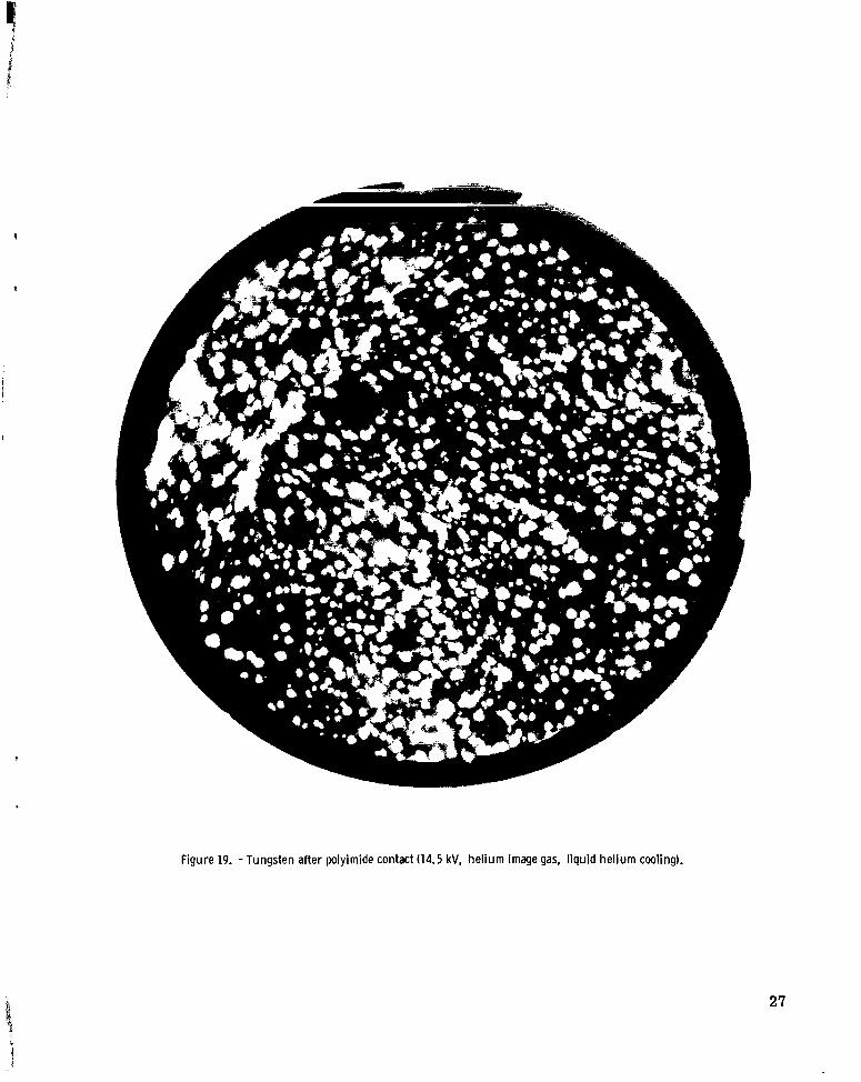
Figure 19. -Tungsten after polyimide contact (14.5 kV, hel ium image gas, liquid hel ium cooling).
27

Figure 20. - Tungsten after polyimide contact (15.0 kV, hel ium image gas, liquid hel ium cooling).
28

4i I
ti
Figure 21. -Tungsten prior to contact (10.5 kV, hel ium image gas, liquid nitrogen cooling).
29

I .-- -Figure 22. -Tungsten after polyimide contact (9.25 kV, helium image gas, liquid helium coaling).
30

Figure 23. -Tungsten affer polyimide contact (9.75 kV, helium image gas, liquid helium cooling).
31
N A T I O N A L A E R O N A U T I C S A N D SPACE A D M I S T R A T I O N W A S H I N G T O N . D.C. 20546
_ _ ~ P O S T A G E A N D FEES P A I D
N A T I O N A L A E R O N A U T I C S A N D O F F I C I A L B U S I N E S S FIRST CLASS MAIL. SPACE A D M I N I S T R A T I O N
P E N A L T Y F O R P R I V A T E USE 5300 USMAIL
021 0 0 1 (31 U 15 717008 S009030S DEPT OF THE A m FORCE A F WEAPONS LAB (AFSC) A
TECH L I B R A R Y / W L O L / BTTN: E LDU BOWMAN, C H I E F K I R T L A N D AFB N M 87117 d
If Undeliverable (Section 158 Posral Manual ) Do Not Return
‘The aeronautical and ;#ace activities of the United Stntes shall be condacted so as to contribute . . . to.-the expansion of human knowledge of phenoniena in the atviosphere and space. The Administration shall provide for the widest practicable and appopriate dissemination of inforiiiation concerning i ts activities and the resrilts thereof.”
-NATIONALAERONAUTICSAND SPACEACT OF 1958
NASA SCIENTIFIC AND TECHNICAL PUBLICATIONS
TECHNICAL REPORTS: Scientific and technical information considered important, complete, and a lasting contribution to existing knowledge.
TECHNICAL NOTES: Information less broad in scope but nevertheless of importance as a contribution to existing knowledge.
TECHNICAL MEMORANDUMS: Information receiving limited distribution because of preliminary data, security classification, or other reasons.
CONTRACTOR REPORTS: Scientific and technical information generated under a NASA contract or grant and considered an important contribution to existing knowledge.
TECHNICAL TRANSLATIONS: Information published in a foreign language considered to merit NASA distribution in English.
SPECIAL PUBLICATIONS: Information derived from or of value to NASA activities. Publications include conference proceedings, monographs, data compilations, handbooks, sourcebooks, and special bibliographies.
TECHNOLOGY UTILIZATION PUBLICATIONS: Information on technology used by NASA that may be of particular interest in commercial and other non-aerospace . applications. Publications include Tech Briefs, . Technology Utilization R~~~~~~and Technology Surveys.
Details on the availability of these publications may be obtained from:
SCIENTIFIC AND TECHNICAL INFORMATION OFFICE
NATIONAL AERONAUTICS AND SPACE ADMINISTRATION Wdrbington, D.C. 40546