adav4601 audio processor for advanced tv ... - analog devices
TRANSCRIPT

Audio Processor for Advanced TV ADAV4601
Rev. B Information furnished by Analog Devices is believed to be accurate and reliable. However, no responsibility is assumed by Analog Devices for its use, nor for any infringements of patents or other rights of third parties that may result from its use. Specifications subject to change without notice. No license is granted by implication or otherwise under any patent or patent rights of Analog Devices. Trademarks and registered trademarks are the property of their respective owners.
One Technology Way, P.O. Box 9106, Norwood, MA 02062-9106, U.S.A.Tel: 781.329.4700 www.analog.com Fax: 781.461.3113 ©2008–2009 Analog Devices, Inc. All rights reserved.
FEATURES Fully programmable 28-bit audio processor for enhanced
ATV sound—default audio processing flow loaded on reset Implements Analog Devices, Inc. and third-party branded
audio algorithms Adjustable digital delay line for audio/video
Synchronization for up to 200 ms stereo delay High performance 24-bit ADC and DAC
94 dB DNR performance on DAC channels 95 dB DNR performance on ADC channels
Headphone output with integrated amplifiers High performance pulse-width modulation (PWM) digital
outputs Multichannel digital baseband I/O
4 stereo synchronous digital I2S input channels One 6-channel sample rate converter (SRC) and one stereo
SRC supporting input sample rates from 5 kHz to 50 kHz One stereo synchronous digital I2S output S/PDIF output with S/PDIF input mux capability
Fast I2C control Operates from 3.3 V (analog), 1.8 V (digital core), and 3.3 V
(digital interface) Available in 80-lead LQFP
APPLICATIONS General-purpose consumer audio post processing
Home audio DVD recorders Home theater in a box systems and DVD receivers
Audio processing subsystems for DTV-ready TVs Analog broadcast capability for iDTVs
GENERAL DESCRIPTION The ADAV4601 is an enhanced audio processor targeting advanced TV applications with full support for digital and analog baseband audio.
The audio processor, by default, loads a dedicated TV audio flow that incorporates full matrix switching (any input to any output), automatic volume control that compensates for volume changes during advertisements or when switching channels, dynamic bass, a multiband equalizer, and up to 200 ms of stereo delay memory for audio-video synchronization.
Alternatively, Analog Devices offers an award-winning graphical programming tool (SigmaStudio™) that allows custom flows to be quickly developed and evaluated. This allows the creation of customer-specific audio flows, including the use of ADI library of third-party algorithms.
The analog I/O integrates Analog Devices proprietary continuous-time, multibit Σ-Δ architecture to bring a higher level of performance to ATV systems, required by third-party algorithm providers to meet system branding certification. The analog input is provided by 95 dB dynamic range (DNR) ADCs, and analog output is provided by 94 dB DNR DACs.
The main speaker outputs can be supplied as a digitally modulated PWM stream to support digital amplifiers.
The ADAV4601 includes multichannel digital inputs and outputs. In addition, digital input channels can be routed through integrated sample rate converters (SRC), which are capable of supporting any arbitrary sample rate from 5 kHz to 50 kHz.

ADAV4601
Rev. B | Page 2 of 60
TABLE OF CONTENTS Features .............................................................................................. 1 Applications ....................................................................................... 1 General Description ......................................................................... 1 Revision History ............................................................................... 3 Functional Block Diagram .............................................................. 4 Specifications ..................................................................................... 5
Performance Parameters ............................................................. 5 Timing Specifications .................................................................. 7 Timing Diagrams .......................................................................... 8
Absolute Maximum Ratings ............................................................ 9 Thermal Resistance ...................................................................... 9 Thermal Conditions ..................................................................... 9 ESD Caution .................................................................................. 9
Pin Configuration and Function Descriptions ........................... 10 Typical Performance Characteristics ........................................... 12 Terminology .................................................................................... 14 Pin Functions .................................................................................. 15
Detailed Pin Descriptions ......................................................... 15 Functional Descriptions ................................................................ 17
Power-Up Sequence ................................................................... 17 Master Clock Oscillator ............................................................. 17 I2C Interface ................................................................................ 17 I2C Read and Write Operations ................................................ 19 ADC Inputs ................................................................................. 19 I2S Digital Audio Inputs ............................................................. 20
DAC Voltage Outputs ................................................................ 22 PWM Outputs ............................................................................ 22 Headphone Output .................................................................... 22 I2S Digital Audio Outputs ......................................................... 23 S/PDIF Input/Output ................................................................. 23 Hardware Mute Control ............................................................ 23 Audio Processor ......................................................................... 23 Graphical Programming Environment ................................... 23 SigmaStudio Pin Assignment ................................................... 24 Application Layer ....................................................................... 24 Loading a Custom Audio Processing Flow ............................. 24 Numeric Formats ....................................................................... 24 ROMs and Registers ................................................................... 25 Safe Loading to Parameter RAM and Target/Slew RAM ...... 25 Read/Write Data Formats ......................................................... 25 Target/Slew RAM ....................................................................... 26 Layout Recommendations ........................................................ 28
Typical Application Diagram ........................................................ 29 Audio Flow Control Registers....................................................... 31
Detailed Register Descriptions ................................................. 31 Main Control Registers .................................................................. 48
Detailed Register Descriptions ................................................. 48 Outline Dimensions ....................................................................... 58
Ordering Guide .......................................................................... 58

ADAV4601
Rev. B | Page 3 of 60
REVISION HISTORY 9/09—Rev. A to Rev. B Changes to Table 11 ........................................................................ 24 Changes to Table 15 ........................................................................ 31 Changes to Table 16 ........................................................................ 32 Changes to Table 40 ........................................................................ 45 Changes to Table 50 ........................................................................ 51 Changes to Table 51 ........................................................................ 53 Changes to Table 54 ........................................................................ 54
4/09—Rev. 0 to Rev. A
Added Advantiv Logo ....................................................................... 1 Changes to General Description Section ....................................... 1 Changes to Figure 1 ........................................................................... 3 Changes to Table 2 ............................................................................ 6 Changes to FILTA and FILTD Section, AVDD Section, and VDD Section .................................................................................... 15 Added Power-Up Sequence Section and Figure 22; Renumbered Sequentially .............................................................. 16 Changes to Master Clock Oscillator Section ............................... 16 Added Table 6, Table 7, Table 8, Table 9, and Figure 23; Renumbered Sequentially .............................................................. 17 Added Figure 24 .............................................................................. 18 Changes to ADC Inputs Section and Figure 25 .......................... 18
Added Figure 31 .............................................................................. 21 Changes to DAC Voltage Outputs Section, Figure 30, PWM Outputs Section, Headphone Output Section, and Figure 33 ... 21 Added Figure 36 .............................................................................. 22 Changes to Hardware Mute Control Section .............................. 22 Added SigmaStudio Pin Assignment Section, Table 10, Table 11, and Numeric Formats Section ....................................................... 23 Changes to Application Layer Section ......................................... 23 Added Figure 38, ROMs and Registers Section, Safe Loading to Parameter RAM and Target/Slew RAM Section, and Read/Write Data Formats Section ..................................................................... 24 Added Target/Slew RAM Section, Table 12, Table 13, and Table 14 ............................................................................................. 25 Added Figure 39, Figure 40, Figure 41, Figure 42, and Figure 43 ........................................................................................... 26 Added Figure 44, Figure 45, Figure 46, and Layout Recommendations Section ............................................................ 27 Changes to Figure 47 ...................................................................... 28 Added Figure 48 .............................................................................. 29 Added Table 15 to Table 61 ............................................................ 30
3/08—Revision 0: Initial Version

ADAV4601
Rev. B | Page 4 of 60
FUNCTIONAL BLOCK DIAGRAM
0707
0-00
1
AUDIOPROCESSOR
ADAV4601A-V
SYNCHRONOUSDELAY
MEMORY
I2C INTERFACE
AD0
SYNCHRONOUSMULTICHANNELDIGITAL INPUTS
6-CHANNEL SRCASYNCHRONOUS
DIGITAL INPUT
2-CHANNEL SRCASYNCHRONOUS
DIGITAL INPUT
SYSTEMCLOCKS
PLL
SPDIF_IN0SPDIF_IN1SPDIF_IN2SPDIF_IN3SPDIF_IN4SPDIF_IN5SPDIF_IN6
SPDIF_OUT/SDO1
S/PDIF I/O
PWMDIGITALOUTPUT
PWM1APWM1BPWM2APWM2BPWM3APWM3BPWM4APWM4B
PWM_READY
BCLK1LRCLK1
SDO0/AD0
HPOUT1L
HPOUT1R
AUXOUT4LAUXOUT4RDAC
AUXOUT1LAUXOUT1RDAC
AUXOUT3LAUXOUT3RDAC
SCLSDA
BCLK2LRCLK2
BCLK0LRCLK0
SDIN0SDIN1SDIN2SDIN3
XOUTMCLKI/XIN
MCLK_OUT
AUXIN1LAUXIN1R ADC
DIGITALOUTPUTS
BCLK1LRCLK1
MUTE
Figure 1. ADAV4601 with PWM-Based Speaker Outputs

ADAV4601
Rev. B | Page 5 of 60
SPECIFICATIONS AVDD = 3.3 V, DVDD = 1.8 V, ODVDD = 3.3 V, operating temperature = −40°C to +85°C, master clock 24.576 MHz, measurement bandwidth = 20 Hz to 20 kHz, ADC input signal = DAC output signal = 1 kHz, unless otherwise noted.
PERFORMANCE PARAMETERS
Table 1. Parameter Min Typ Max Unit Test Conditions/Comments REFERENCE SECTION
Absolute Voltage VREF 1.53 V VREF Temperature Coefficient 100 ppm/°C
ADC SECTION Number of Channels 2 One stereo channel Full-Scale Input Level 100 μA rms Resolution 24 Bits Dynamic Range (Stereo Channel)
A-Weighted 95 dB −60 dBFS with respect to full-scale analog input Total Harmonic Distortion + Noise
(Stereo Channel) −90 dB −3 dBFS with respect to full-scale analog input
Gain Mismatch 0.2 dB Left- and right-channel gain mismatch Crosstalk (Left-to-Right, Right-to-Left) −110 dB Gain Error −1 dB Input signal is 100 μA rms
Current Setting Resistor (RISET) 20 kΩ External resistor to set current input range of ADC for nominal 2.0 V rms input signal
Power Supply Rejection −87 dB 1 kHz, 300 mV p-p signal at AVDD ADC DIGITAL DECIMATOR FILTER
CHARACTERISTICS At 48 kHz, guaranteed by design
Pass Band 22.5 kHz Pass-Band Ripple ±0.0002 dB Stop Band 26.5 kHz Stop-Band Attenuation 100 dB Group Delay 1040 μs
PWM SECTION Frequency 384 kHz Guaranteed by design Modulation Index 0.976 Guaranteed by design Dynamic Range
A-Weighted 98 dB −60 dBFS with respect to full-scale code input Total Harmonic Distortion + Noise −80 dB −3 dBFS with respect to full-scale code input
DAC SECTION Number of Auxiliary Output Channels 6 Three stereo channels Resolution 24 Bits Full-Scale Analog Output 1 V rms Dynamic Range
A-Weighted 94 dB −60 dBFS with respect to full-scale code input Total Harmonic Distortion + Noise −86 dB −3 dBFS with respect to full-scale code input Crosstalk (Left-to-Right, Right-to-Left) −102 dB Interchannel Gain Mismatch 0.1 dB Left- and right-channel gain mismatch Gain Error 0.525 dB 1 V rms output DC Bias 1.53 V Power Supply Rejection −90 dB 1 kHz, 300 mV p-p signal at AVDD Output Impedance 235 Ω

ADAV4601
Rev. B | Page 6 of 60
Parameter Min Typ Max Unit Test Conditions/Comments DAC DIGITAL INTERPOLATION FILTER
CHARACTERISTICS At 48 kHz, guaranteed by design
Pass Band 21.769 kHz Pass-Band Ripple ±0.01 dB Transition Band 23.95 kHz Stop Band 26.122 kHz Stop-Band Attenuation 75 dB Group Delay 580 μs
HEADPHONE AMPLIFIER Measured at headphone output with 32 Ω load Number of Channels 2 One stereo channel Full-Scale Output Power 31 mW rms 1 V rms output Dynamic Range
A-Weighted 93 dB −60 dBFS with respect to full-scale code input Total Harmonic Distortion + Noise −83 dB −3 dBFS with respect to full-scale code input Interchannel Gain Mismatch 0.1 dB DC Bias 1.53 V Power Supply Rejection −85 dB 1 kHz, 300 mV p-p signal at AVDD
SRC Number of Channels 8 Two channels (SRC1), six channels (SRC2) Dynamic Range
A-Weighted 115 dB −60 dBFS input (worst-case input fS = 50 kHz) Total Harmonic Distortion + Noise −113 dB −3 dBFS input (worst-case input fS = 50 kHz) Sample Rate 5 50 kHz
SRC DIGITAL INTERPOLATION FILTER CHARACTERISTICS
At 48 kHz, guaranteed by design
Pass Band 21.678 kHz Pass-Band Ripple 0.005 dB Stop Band 26.232 kHz Stop-Band Attenuation 110 dB Group Delay 876 μs
DIGITAL INPUT/OUTPUT Input Voltage High (VIH) 2.0 ODVDD V Input Voltage Low (VIL) 0.8 V Input Leakage
IIH (SDIN0, SDIN1, SDIN2, SDIN3, LRCLK0, LRCLK1, LRCLK2, BCLK0, BCLK1, BCLK2, SPDIF_OUT, SPDIF_IN)
40 μA VIH = ODVDD, equivalent to a 90 kΩ pull-up resistor
IIH (RESET) 13.5 μA VIH = ODVDD, equivalent to a 266 kΩ pull-up resistor
IIL (SDO0, SCL, SDA) −40 μA VIL = 0 V, equivalent to a 90 kΩ pull-down resistor Output Voltage High (VOH) 2.4 V IOH = 0.4 mA Output Voltage Low (VOL) 0.4 V IOL = −2 mA Output Voltage High (VOH) (MCLK_OUT) 1.4 V IOH = 0.4 mA Output Voltage Low (VOL) (MCLK_OUT) 0.4 V IOL = −3.2 mA Input Capacitance 10 pF
SUPPLIES Analog Supplies (AVDD) 3.0 3.3 3.6 V Digital Supplies (DVDD) 1.65 1.8 2.0 V Interface Supply (ODVDD) 3.0 3.3 3.6 V Supply Currents MCLK = 24 MHz, ADCs and DACs active, headphone
outputs active and driving a 16 Ω load Analog Current 115 mA Digital Current 160 mA Interface Current 2 mA

ADAV4601
Rev. B | Page 7 of 60
Parameter Min Typ Max Unit Test Conditions/Comments Power Dissipation 0.674 W Standby Currents ADC, DAC, and headphone outputs floating,
RESET low, MCLK = 24 MHz
Analog Current 7 mA Digital Current 3 mA Interface Current 1.6 mA
TEMPERATURE RANGE Operating Temperature −40 +85 °C Storage Temperature −65 +150 °C
TIMING SPECIFICATIONS
Table 2. Parameter Description Min Max Unit Comments MASTER CLOCK AND RESET
fMCLKI MCLKI frequency 3.072 24.576 MHz tMP MCLKI period 40 325 ns tMCH MCLKI high 10 ns tMCL MCLKI low 10 ns tRESET RESET low 200 ns
MASTER CLOCK OUTPUT tCK MCLK_OUT period 8 162 ns tJIT
Period jitter 800 ps tCH MCLK_OUT high 45 55 % tCL MCLK_OUT low 45 55 %
I2C PORT fSCL SCL clock frequency 400 kHz tSCLH SCL high 600 ns tSCLL SCL low 1.3 μs Start Condition
tSCS Setup time 600 ns Relevant for repeated start condition tSCH Hold time 600 ns After this period, the first clock is generated tDS Data setup time 100 ns tSCR SCL rise time 300 ns tSCF SCL fall time 300 ns tSDR SDA rise time 300 ns tSDF SDA fall time 300 ns
Stop Condition tSCS Setup time 0 ns
SERIAL PORTS Slave Mode
tSBH BCLK high 40 ns tSBL BCLK low 40 ns fSBF BCLK frequency 64 × fS tSLS LRCLK setup 10 ns To BCLK rising edge tSLH LRCLK hold 10 ns From BCLK rising edge tSDS SDIN setup 10 ns To BCLK rising edge tSDH SDIN hold 10 ns From BCLK rising edge tSDD SDO delay 50 ns From BCLK falling edge
Master Mode tMLD LRCLK delay 25 ns From BCLK falling edge tMDD SDO delay 15 ns From BCLK falling edge tMDS SDIN setup 10 ns From BCLK rising edge tMDH SDIN hold 10 ns From BCLK rising edge

ADAV4601
Rev. B | Page 8 of 60
TIMING DIAGRAMS
MCLKI
RESET
tMP = 1/fMCLKI tMCH tMCL
tRESET 0707
0-00
4
Figure 2. Master Clock and Reset Timing
0707
0-03
5
tJIT
tCH tCL
tCK
DVDD
GND
Figure 3. Master Clock Output Timing
LRCLK1
BCLK1
SDINx
SDO0
tSLS
tSLH
tSDS tSDH
tSDD 0707
0-00
2
Figure 4. Serial Port Slave Mode Timing
LRCLK1
BCLK1
SDINx
SDO0
tMLD
tMDS tMDH
tMDD 0707
0-00
3
Figure 5. Serial Port Master Mode Timing
0707
0-03
2
ODVDD
100µA IOL
100µA IOH
TO OUTPUTPIN
50pF
Figure 6. Load Circuit for Digital Output Timing Specifications
0707
0-03
3
DVDD
1.8V
0V
3.3V
0V
AVDDODVDD
1.0s MAX
1.0s MAX
1.65V
3.0V
0.33V
0.18V
Figure 7. Power-Up Sequence Timing
0707
0-03
4
DVDD
1.8V
0V
3.3V
0V
AVDDODVDD
1.0s MAX
1.0s MAX
1.65V
3.0V
0.33V
0.18V
Figure 8. Power-Down Sequence Timing

ADAV4601
Rev. B | Page 9 of 60
ABSOLUTE MAXIMUM RATINGS Table 3. Parameter Rating DVDD to DGND 0 V to 2.2 V ODVDD to DGND 0 V to 4 V AVDD to AGND 0 V to 4 V AGND to DGND −0.3 V to +0.3 V Digital Inputs DGND − 0.3 V to ODVDD + 0.3 V Analog Inputs AGND − 0.3 V to AVDD + 0.3 V Reference Voltage Indefinite short circuit to ground Soldering (10 sec) 300°C
Stresses above those listed under Absolute Maximum Ratings may cause permanent damage to the device. This is a stress rating only; functional operation of the device at these or any other conditions above those indicated in the operational section of this specification is not implied. Exposure to absolute maximum rating conditions for extended periods may affect device reliability.
THERMAL RESISTANCE θJA is specified for the worst-case conditions, that is, a device soldered in a circuit board for surface-mount packages. Thermal resistance is based on JEDEC 2S2P PCB.
Table 4. Package Type θJA θJC Unit 80-Lead LQFP 38.1 7.6 °C/W
THERMAL CONDITIONS To ensure correct operation of the device, the case temperature (TCASE) must be kept below 121°C to keep the junction temperature (TJ) below the maximum allowed, 125°C.
ESD CAUTION

ADAV4601
Rev. B | Page 10 of 60
PIN CONFIGURATION AND FUNCTION DESCRIPTIONS
VREFAGNDAVDD
NCNCNC
FILTA
NCNCNC
NCDGNDDVDDMUTE
SDASCL
SPDIF_IN5/LRCLK2SPDIF_IN6/BCLK2
DGND
2
3
4
7
6
5
1
8
9
10
12
13
14
15
16
17
18
19
20
11NC
AVDDHPOUT1RHPOUT1L
PLL_LFAGNDAGND
NC
NC = NO CONNECT
AVDDDGNDDVDD
PWM4BPWM4APWM3BPWM3APWM2BPWM2APWM1BPWM1ADGND
59
58
57
54
55
56
60
53
52
51
49
48
47
46
45
44
43
42
41
50 RESET
21
DVD
D
22
SDIN
0
23
SDIN
1
24
SDIN
2
25
SPD
IF_I
N0/
SDIN
3
26
SPD
IF_I
N1/
LRC
LK0
27
SPD
IF_I
N2/
BC
LK0
28
OD
GN
D
29
OD
VDD
30
MC
LK_O
UT
31
DVD
D
32
DG
ND
33
MC
LKI/X
IN
34
XOU
T
35
SPD
IF_I
N4/
BC
LK1
36
SPD
IF_I
N3/
LRC
LK1
37
SDO
0/A
D0
38SP
DIF
_OU
T/SD
O1
39PW
M_R
EAD
Y40
DVD
D
ISET
AU
XIN
1RA
UXI
N1L
NC
NC
NC
NC
AU
XOU
T1R
AU
XOU
T1L
AVD
DA
GN
DA
GN
DA
VDD
FILT
DN
CA
UXO
UT4
RA
UXO
UT4
LA
UXO
UT3
RA
UXO
UT3
LN
C
80 79 78 77 76 75 74 73 72 71 70 69 68 67 66 65 64 63 62 61
PIN 1
ADAV4601TOP VIEW
(Not to Scale)
0707
0-00
6
Figure 9. Pin Configuration
Table 5. Pin Function Descriptions Pin No. Mnemonic Description 1 FILTA ADC Filter Capacitor. 2 VREF Reference Capacitor. 3 AGND ADC Ground. 4 AVDD ADC Supply (3.3 V). 5 to 12 NC No Connection to This Pin Allowed. 13 DGND Digital Ground. 14 DVDD Digital Supply (1.8 V). 15 MUTE Active-Low Mute Request Input Signal.
16 SDA I2C Data. 17 SCL I2C Clock. 18 SPDIF_IN5/LRCLK2 External Input to S/PDIF Mux/Left/Right Clock for SRC2 (Default). 19 SPDIF_IN6/BCLK2 External Input to S/PDIF Mux/Bit Clock for SRC2 (Default). 20 DGND Digital Ground. 21 DVDD Digital Supply (1.8 V). 22 SDIN0 Serial Data Input 0/SRC Data Input. 23 SDIN1 Serial Data Input 1/SRC Data Input. 24 SDIN2 Serial Data Input 2/SRC Data Input.

ADAV4601
Rev. B | Page 11 of 60
Pin No. Mnemonic Description 25 SPDIF_IN0/SDIN3 External Input to S/PDIF Mux/SRC Data Input/Serial Data Input 3 (Default). 26 SPDIF_IN1/LRCLK0 External Input to S/PDIF Mux/Left/Right Clock for SRC1 (Default). 27 SPDIF_IN2/BCLK0 External Input to S/PDIF Mux/Bit Clock for SRC1 (Default). 28 ODGND Digital Ground. 29 ODVDD Digital Interface Supply (3.3 V). 30 MCLK_OUT Master Clock Output. 31 DVDD Digital Supply (1.8 V). 32 DGND Digital Ground. 33 MCLKI/XIN Master Clock/Crystal Input. 34 XOUT Crystal Output. 35 SPDIF_IN4/BCLK1 External Input to S/PDIF Mux/Bit Clock for Serial Data I/O (Default). 36 SPDIF_IN3/LRCLK1 External Input to S/PDIF Mux/Left/Right Clock for Serial Data I/O (Default). 37 SDO0/AD0 Serial Data Output. This pin acts as the I2C address select on reset. It has an internal pull-down resistor.
38 SPDIF_OUT/SDO1 Output of S/PDIF Mux/Serial Data Output. 39 PWM_READY PWM Ready Flag. 40 DVDD Digital Supply (1.8 V). 41 DGND Digital Ground. 42 PWM1A Pulse-Width Modulated Output 1A. 43 PWM1B Pulse-Width Modulated Output 1B. 44 PWM2A Pulse-Width Modulated Output 2A. 45 PWM2B Pulse-Width Modulated Output 2B. 46 PWM3A Pulse-Width Modulated Output 3A. 47 PWM3B Pulse-Width Modulated Output 3B. 48 PWM4A Pulse-Width Modulated Output 4A. 49 PWM4B Pulse-Width Modulated Output 4B. 50 RESET Reset Analog and Digital Cores.
51 DVDD Digital Supply (1.8 V). 52 DGND Digital Ground. 53 AVDD PLL Supply (3.3 V). 54 PLL_LF PLL Loop Filter. 55 AGND PLL Ground. 56 AGND Headphone Driver Ground. 57 HPOUT1L Left Headphone Output. 58 HPOUT1R Right Headphone Output. 59 AVDD Headphone Driver Supply (3.3 V). 60, 61 NC No Connection to This Pin Allowed. 62 AUXOUT3L Left Auxiliary Output 3. 63 AUXOUT3R Right Auxiliary Output 3. 64 AUXOUT4L Left Auxiliary Output 4. 65 AUXOUT4R Right Auxiliary Output 4. 66 NC No Connection to This Pin Allowed. 67 FILTD DAC Filter Capacitor. 68 AVDD DAC Supply (3.3 V). 69 AGND DAC Ground. 70 AGND DAC Ground. 71 AVDD DAC Supply (3.3 V). 72 AUXOUT1L Left Auxiliary Output 1. 73 AUXOUT1R Right Auxiliary Output 1. 74 to 77 NC No Connection to This Pin Allowed. 78 AUXIN1L Left Auxiliary Input 1. 79 AUXIN1R Right Auxiliary Input 1. 80 ISET ADC Current Setting.

ADAV4601
Rev. B | Page 12 of 60
TYPICAL PERFORMANCE CHARACTERISTICS 0
–180
–160
0 7
MA
GN
ITU
DE
(dB
)
FREQUENCY (kHz)192 384 576
–140
–120
–100
–80
–60
–40
–20
68
0707
0-00
7
Figure 10. DAC Composite Filter Response (48 kHz)
0
–1600 9
MA
GN
ITU
DE
(dB
)
FREQUENCY (kHz)24 48 72
–140
–120
–100
–80
–60
–40
–20
6
0707
0-00
8
Figure 11. DAC Pass-Band Filter Response (48 kHz)
0.6
–0.6
–0.4
–0.2
0
0.2
0.4
0 2
MA
GN
ITU
DE
(dB
)
FREQUENCY (kHz)8 16 4
0707
0-00
9
Figure 12. DAC Pass-Band Ripple (48 kHz)
0
–30
–60
–90
–120
–150
–180
–210
–240
–270
–3000 3
MA
GN
ITU
DE
(dB
)
FREQUENCY (kHz)128 256 84
0707
0-01
0
Figure 13. ADC Composite Filter Response (48 kHz)
0
–180
–150
–120
–90
–60
–30
0 9
MA
GN
ITU
DE
(dB
)
FREQUENCY (kHz)24 48 72 6
0707
0-01
1
Figure 14. ADC Pass-Band Filter Response (48 kHz)
0.04
–0.04
–0.03
–0.02
–0.01
0
0.01
0.02
0.03
0 2
MA
GN
ITU
DE
(dB
)
FREQUENCY (kHz)8 16 4
0707
0-01
2
Figure 15. ADC Pass-Band Ripple (48 kHz)

ADAV4601
Rev. B | Page 13 of 60
0
–1600 20000
MA
GN
ITU
DE
(dB
V)
FREQUENCY (Hz)4000 8000 12000 16000
–140
–120
–100
–80
–60
–40
–20
0707
0-01
3
Figure 16. DAC Dynamic Range
0
–1600 20000
MA
GN
ITU
DE
(dB
V)
FREQUENCY (Hz)4000 8000 12000 16000
–140
–120
–100
–80
–60
–40
–20
0707
0-01
4
Figure 17. DAC Total Harmonic Distortion + Noise
0
–160
MA
GN
ITU
DE
(dB
V)
–140
–120
–100
–80
–60
–40
–20
0707
0-01
5
0 20000FREQUENCY (Hz)
4000 8000 12000 16000
Figure 18. ADC Dynamic Range
0
–160
MA
GN
ITU
DE
(dB
V)
–140
–120
–100
–80
–60
–40
–20
0707
0-01
6
0 20000FREQUENCY (Hz)
4000 8000 12000 16000
Figure 19. ADC Total Harmonic Distortion + Noise
0
–140
–120
–100
–80
–60
–40
–20
0 10.90.80.70.60.50.40.30.20.1
GA
IN (d
B)
NORMALIZED FREQUENCY 0707
0-01
7
.0
Figure 20. Sample Rate Converter Transfer Function

ADAV4601
Rev. B | Page 14 of 60
TERMINOLOGY Dynamic Range The ratio of a full-scale input signal to the integrated input noise in the pass band (20 Hz to 20 kHz), expressed in decibels (dB). Dynamic range is measured with a −60 dB input signal and is equal to (S/[THD+N]) + 60 dB. Note that spurious harmonics are below the noise with a −60 dB input; therefore, the noise level establishes the dynamic range. The dynamic range is specified with and without an A-weight filter applied.
Pass Band The region of the frequency spectrum unaffected by the attenuation of the filter of the digital decimator.
Pass-Band Ripple The peak-to-peak variation in amplitude response from equal amplitude input signal frequencies within the pass band, expressed in decibels.
Stop Band The region of the frequency spectrum attenuated by the filter of the digital decimator to the degree specified by stop-band attenuation.
Gain Error With a near full-scale input, the ratio of the actual output to the expected output, expressed in dB.
Interchannel Gain Mismatch With identical near full-scale inputs, the ratio of the outputs of the two stereo channels, expressed in decibels.
Crosstalk Ratio of response on one channel with a grounded input to a full-scale 1 kHz sine wave input on the other channel, expressed in decibels.
Power Supply Rejection With no analog input, the signal present at the output when a 300 mV p-p signal is applied to power supply pins, expressed in decibels of full scale.
Group Delay Intuitively, the time interval required for an input pulse to appear at the output of the converter, expressed in milliseconds (ms); more precisely, the derivative of radian phase with respect to radian frequency at a given frequency.

ADAV4601
Rev. B | Page 15 of 60
PIN FUNCTIONS DETAILED PIN DESCRIPTIONS Table 5 shows the pin numbers, mnemonics, and descriptions for the ADAV4601. The input pins have a logic threshold compatible with 3.3 V input levels.
SDIN0, SDIN1, SDIN2, and SDIN3/SPDIF_IN0
Serial data inputs. These input pins provide the digital audio data to the signal processing core. Any of the inputs can be routed to either of the SRCs for conversion; this input is then not available as a synchronous input to the audio processor but only as an input through the selected SRC. The serial format for the synchronous data is selected by Bits[3:2] of the Serial Port Control Register 1. If the SRCs are required, the serial format is selected by Bits[12:9] of the same register. The synchronous inputs are capable of using any pair of serial clocks, LRCLK0/BCLK0, LRCLK1/BCLK1, or LRCLK2/BCLK2. By default, they use LRCLK1 and BCLK1. See Figure 26 for more details regarding the configuration of the synchronous inputs.
SDIN3 is a shared pin with SPDIF_IN0. If SDIN3 is not in use, this pin can be used to connect an S/PDIF signal from an external source, such as an MPEG decoder, to the ADAV4601 on-chip S/PDIF output multiplexer. If SPDIF_OUT is selected from one of the SPDIF_IN (external) signals, the signal is simply passed through from input to output.
LRCLK0/SPDIF_IN1, BCLK0/SPDIF_IN2, LRCLK1/SPDIF_IN3, BCLK1/SPDIF_IN4, LRCLK2/SPDIF_IN5, and BCLK2/SPDIF_IN6
By default, LRCLK1 and BCLK1 are associated with the synchronous inputs, LRCLK0 and BCLK0 are associated with SRC1, and LRCLK2 and BCLK2 are associated with SRC2. However, the SRCs and synchronous inputs can use any of the serial clocks (see Figure 26). LRCLK0, BCLK0, LRCLK1, BCLK1, LRCLK2, and BCLK2 are shared pins with SPDIF_IN1, SPDIF_IN2, SPDIF_IN3, SPDIF_IN4, SPDIF_IN5, and SPDIF_IN6, respectively. If LRCLK0/LRCLK1/ LRCLK2 or BCLK0/BCLK1/BCLK2 are not in use, these pins can be used to connect an S/PDIF signal from an external source, such as an MPEG decoder, to the ADAV4601 on-chip S/PDIF output multiplexer. If SPDIF_OUT is selected from one of the SPDIF_IN (external) signals, the signal is simply passed through from input to output.
SDO0/AD0
Serial data output. This pin can output two channels of digital audio using a variety of standard 2-channel formats. The clocks for SDO0 are always the same as those used by the synchronous inputs; therefore, LRCLK1 and BCLK1 are used by default, although SDO0 is capable of using any pair of serial clocks, LRCLK0/BCLK0, LRCLK1/BCLK1, or LRCLK2/BCLK2. The Serial Port Control Register 1 selects the serial format for the synchronous output. On reset, the SDO0 pin duplicates as the I2C® address select pin. In this mode, the logical state of the pin is polled for four MCLKI cycles following reset. The address select bit is set as the majority poll of the logic level of the pin after the four MCLKI cycles.
SPDIF_OUT/SDO1
The ADAV4601 contains an S/PDIF multiplexer functionality that allows the SPDIF_OUT signal to be chosen from an internally generated S/PDIF signal or from the S/PDIF signal of an external source, which is connected via one of the SPDIF_IN pins. This pin can also be configured as an additional serial output (SDO1) as an alternate function.
MCLKI/XIN
Master clock input. The ADAV4601 uses a PLL to generate the appropriate internal clock for the audio processing core. A clock signal of a suitable frequency can be connected directly to this pin, or a crystal can be connected between MCLKI/XIN and XOUT together with the appropriate capacitors to DGND to generate a suitable clock signal.
XOUT
This pin is used in conjunction with MCLKI/XIN to generate a clock signal for the ADAV4601.
MCLK_OUT
This pin can be used to output MCLKI or one of the internal system clocks. Note that the output level of this pin is referenced to DVDD (1.8 V) and not ODVDD (3.3 V) like all the other digital inputs and outputs.
SDA
Serial data input for the I2C control port. SDA features a glitch elimination filter that removes spurious pulses that are less than 50 ns wide.
ADAV4601
Rev. B | Page 16 of 60
SCL
Serial clock for the I2C control port. SCL features a glitch elimination filter that removes spurious pulses that are less than 50 ns wide.
MUTE
Mute input request. This active-low input pin controls the muting of the output ports (both analog and digital) from the ADAV4601. When low, it asserts mute on the outputs that are enabled in the audio flow.
RESET
Active-low reset signal. After RESET goes high, the circuit blocks are powered down. The blocks can be individually powered up with software. When the part is powered up, it takes approximately 3072 internal clocks to initialize the internal circuitry. The internal system clock is equal to MCLKI until the PLL is powered and enabled, after which the internal system clock becomes 2560 × fS (122.88 MHz). When the PLL is powered up and enabled after reset, it takes approximately 3 ms to lock. When the audio processor is enabled, it takes approximately 32,768 internal system clocks to initialize and load the default flow to the audio processor memory. The audio processor is not available during this time.
AUXIN1L AND AUXIN1R
Analog inputs to the on-chip ADCs.
AUXOUT1L, AUXOUT1R, AUXOUT3L, AUXOUT3R, AUXOUT4L, and AUXOUT4R
Auxiliary DAC analog outputs. These pins can be programmed to supply the outputs of the internal audio processing for line out or record use.
HPOUT1L and HPOUT1R
Analog outputs from the headphone amplifiers.
PLL_LF
PLL loop filter connection. A 100 nF capacitor and a 2 kΩ resistor in parallel with a 1 nF capacitor tied to AVDD are required for the PLL loop filter to operate correctly.
VREF
Voltage reference for DACs and ADCs. This pin is driven by an internal 1.5 V reference voltage.
FILTA and FILTD
Decoupling nodes for the ADC and DAC. Decoupling capacitors should be connected between these nodes and AGND, typically 47 μF in parallel with 0.1 μF and 10 μF in parallel with 0.1 μF, respectively.
PWM1A, PWM1B, PWM2A, PWM2B, PWM3A, PWM3B, PWM4A, and PWM4B
Differential pulse-width modulation outputs are suitable for driving Class-D amplifiers.
PWM_READY
This pin is set high when PWM is enabled and stable.
AVDD
Analog power supply pins. These pins should be connected to 3.3 V. Each AVDD pin should be decoupled with a 0.1 μF capacitor to AGND, as close to the pin as possible. In addition, the ADC supply (Pin 4) and the DAC supplies (Pin 68 and Pin 71) should share a 10 μF capacitor to ground. The PLL supply (Pin 53) should have an additional 1 nF and 10 μF capacitor to ground, and the headphone supply (Pin 59) should have an additional 10 μF capacitor to ground.
DVDD
Digital power supply pins. These pins should be connected to a 1.8 V digital supply. For optimal performance, each DVDD/DGND pair requires a 0.1 μF decoupling capacitor as close to the pin as possible. In addition, these 0.1 μF decoupling capacitors are in parallel with a single 10 μF capacitor.
ODVDD
Digital interface power supply pin. Connect this pin to a 3.3 V digital supply. Decouple this pin with 10 μF and 0.1 μF capacitors to DGND, as close to the pin as possible.
DGND
Digital ground.
AGND
Analog ground.
ODGND
Ground for the digital interface power supply.
ISET
ADC current setting resistor. See the ADC Inputs section for more details.

ADAV4601
Rev. B | Page 17 of 60
FUNCTIONAL DESCRIPTIONS POWER-UP SEQUENCE The following sequence provides an overview of how to initialize the IC:
1. Apply power to the ADAV4601.
2. Enable PLL via an I2C write and wait 15 ms for PLL to lock.
3. Power up via an I2C write to the global power-up bit in the initialization control register (0x0000).
4. A default flow is automatically loaded on power-up. If a user-defined flow is loaded, see the Loading a Custom Audio Processing Flow section for additional information.
5. Depending on the I/O blocks required, other steps may need to be taken; for example, headphone outputs may need to be tristated. See the ADC Inputs, DAC Voltage Outputs, PWM Outputs, Headphone Output and S/PDIF Input/Output sections that describe the I/O blocks in detail.
6. Unmute.
MASTER CLOCK OSCILLATOR Internally, the ADAV4601 operates synchronously to the master MCLKI input. All internal system clocks are generated from this single clock input using an internal PLL. This MCLKI input can also be generated by an external crystal oscillator connected to the MCLKI/XIN pin or by using a simple crystal oscillator connected across MCLKI/XIN and XOUT. By default, the master clock frequency is 24.576 MHz; however, by using the internal dividers, an MCLKI of 12.288 MHz, 6.144 MHz, and 3.072 MHz are also supported.
OSC
DIVIDER
REGISTER
DIVIDER WORD[÷8, ÷4, ÷2, ÷1]
3.072MHz PLLREFERENCECLOCK
MASTER CLOCK FREQUENCY[24.576MHz, 12.288MHz,6.144MHz, 3.072MHz]
I2C
EXTERNAL CLOCK/CRYSTAL
0707
0-01
8
Figure 21. Master Clock
Figure 22 shows the external circuit recommended for proper operation when using a crystal oscillator. Due to the effect of stray capacitance, consideration must be given to the value of C1 and C2 when calculating the desired CLOAD for the crystal.
Spgpg
pgpgLOAD C
CCCC
CCCCC +
+++
++=
21
)2)(1(
21
21
where: Cpg1 and Cpg2 are the pin to ground capacitances. CS is the PCB stray capacitance.
A good rule of thumb is to approximate Cpg1 and Cpg2 to be between 5 pF and 10 pF and CS to be between 2 pF and 3 pF.
C1
C2
XIN
XOUT
0707
0-10
0
Figure 22. Circuit for Crystal Resonator
I2C INTERFACE The ADAV4601 supports a 2-wire serial (I2C compatible) microprocessor bus driving multiple peripherals. The ADAV4601 is controlled by an external I2C master device, such as a micro-controller. The ADAV4601 is in slave mode on the I2C bus, except during self-boot. While the ADAV4601 is self-booting, it becomes the master, and the EEPROM, which contains the ROMs to be booted, is the slave. When the self-boot process is complete, the ADAV4601 reverts to slave mode on the I2C bus. No other devices should access the I2C bus while the ADAV4601 is self-booting (refer to the Application Layer section and the Loading a Custom Audio Processing Flow section).
Initially, all devices on the I2C bus are in an idle state, wherein the devices monitor the SDA and SCL lines for a start condition and the proper address. The I2C master initiates a data transfer by establishing a start condition, defined by a high-to-low transition on SDA while SCL remains high. This indicates that an address/ data stream follows. All devices on the bus respond to the start condition and read the next byte (7bit address plus the R/W bit) MSB first. The device that recognizes the transmitted address responds by pulling the data line low during the ninth clock pulse. This ninth bit is known as an acknowledge bit.
All other devices on the bus revert to an idle condition. The R/W bit determines the direction of the data. A Logic Level 0 on the LSB of the first byte means the master writes information to the peripheral. A Logic Level 1 on the LSB of the first byte means the master reads information from the peripheral. A data transfer takes place until a stop condition is encountered. A stop condition occurs when SDA transitions from low to high while SCL is held high.
The ADAV4601 determines its I2C device address by sampling the SDO0 pin after reset. Internally, the SDO0 pin is sampled by four MCLKI edges to determine the state of the pin (high or low). Because the pin has an internal pull-down resistor default, the address of the ADAV4601 is 0x34 (write) and 0x35 (read). An alternate address, 0x36 (write) and 0x37 (read), is available by tying the SDO0 pin to ODVDD via a 10 kΩ resistor. The I2C interface supports a clock frequency of up to 400 kHz.

ADAV4601
Rev. B | Page 18 of 60
Table 6. Single Word I2C Write1 S Chip address,
R/W = 0 AS Subaddress high AS Subaddress low AS Data Byte 1 AS Data Byte 2 … AS Data Byte N P
1 S = start bit, P = stop bit, and AS = acknowledge by slave.
Table 7. Burst Mode I2C Write1 S Chip
address, R/W = 0
AS Subaddress high
AS Subaddress low
AS Data-Word 1, Byte 1
AS Data-Word 1, Byte 2
AS Data-Word 2, Byte 1
AS Data-Word 2, Byte 2
AS … P
1 S = start bit, P = stop bit, and AS = acknowledge by slave.
Table 8. Single Word I2C Read1 S Chip address,
R/W = 0 AS Subaddress
high AS Subaddress
low AS S Chip address,
R/W = 1 AS Data Byte 1 AM Data
Byte 2 … AM Data
Byte N P
1 S = start bit, P = stop bit, AM = acknowledge by master, and AS = acknowledge by slave.
Table 9. Burst Mode I2C Read1 S Chip address,
R/W = 0 AS Subaddress
high AS Subaddress
low AS S Chip address,
R/W = 1 AS Data-Word 1
Byte 1 AM Data-Word 1
Byte 2 AM … P
1 S = start bit, P = stop bit, AM = acknowledge by master, and AS = acknowledge by slave.
R/W0
SCL
SCL(CONTINUED)
SDA(CONTINUED)
SDA 0 1 0 ADRSEL1 0
FRAME 1CHIP ADDRESS BYTE
START BYMASTER
ACK BYADAV4601
ACK BYADAV4601
FRAME 2SUBADDRESS BYTE 1
FRAME 2SUBADDRESS BYTE 2
ACK BYADAV4601
ACK BYADAV4601
STOP BYMASTER
0707
0-10
1
FRAME 3DATA BYTE 1
Figure 23. I2C Write Format

ADAV4601
Rev. B | Page 19 of 60
R/W
R/W
0 0 1 0 1 0
0 0 1 0 1 0
ADRSEL
ADRSEL
SCL
SCL(CONTINUED)
SDA(CONTINUED)
SCL(CONTINUED)
SDA(CONTINUED)
SDA
FRAME 1CHIP ADDRESS BYTE
START BYMASTER
ACK BYADAV4601
ACK BYADAV4601
FRAME 2SUBADDRESS BYTE 1
FRAME 3SUBADDRESS BYTE 2
ACK BYADAV4601
REPEATEDSTART BYMASTER
ACK BYADAV4601
FRAME 4CHIP ADDRESS BYTE
FRAME 5READ DATA BYTE 1
ACK BYMASTER
ACK BYMASTER
FRAME 6READ DATA BYTE 1
STOP BYMASTER
0707
0-10
2
Figure 24. I2C Read Format
I2C READ AND WRITE OPERATIONS ADC INPUTS Table 6 shows the timing of a single word write operation. Every ninth clock, the ADAV4601 issues an acknowledge by pulling SDA low.
The ADAV4601 has two ADC inputs. By default, this is configured as a single stereo input; however, because the audio processor is programmable, these inputs can be reconfigured.
Table 7 shows the timing of the burst mode write sequence. Table 7 shows an example where the target destination registers are two bytes. The ADAV4601 auto-increments its subaddress register counter every two bytes until a stop condition occurs.
The ADC inputs are shown in Figure 25. The analog inputs are current inputs (100 μA rms FS) with a 1.5 V dc bias voltage. Any input voltage can be accommodated by choosing a suitable combination of input resistor (RIN) and ISET resistor (RISET) using the formulas The timing of a single word read operation is shown in Table 8.
Note that the first R/W bit is still 0, indicating a write operation. This is because the subaddress must be written to set up the internal address. After the ADAV4601 acknowledges the receipt of the subaddress, the master must issue a repeated start command followed by the chip address byte with the R/W set to 1 (read). The ADAV4601 responds with the read result on SDA. The master then responds every ninth clock with an acknowledge pulse to the ADAV4601.
RIN = VFS rms/100 μA rms
RISET = 2RIN/VIN
Resistor matching (typically 1%) between RIN and RISET is important to ensure a full-scale signal on the ADC without clipping. A 10 μF dc blocking capacitor is also required at the input.
After reset, the ADCs are in a power-down state. The ADCs can be powered up using the global power-up in the initialization control register (0x0000). In power critical applications, it is possible to use the analog power management register (0x0005) to power-up or power-down individual ADCs.
Table 9 shows the timing of the burst mode read sequence. Table 9 shows an example where the target read registers are two bytes. The ADAV4601 increments its subaddress register every two bytes because the requested subaddress corresponds to a register or memory area with word lengths of two bytes. Other address ranges may have a variety of word lengths ranging from one to six bytes; the ADAV4601 always decodes the subaddress and sets the auto-increment circuit so that the address increments after the appropriate number of bytes.
DC BIAS1.5V
24-BIT
ADC
20kΩ
ANALOG INPUT100µA rms
FULL SCALE
DC BIAS1.5V
24-BIT
ADC
20kΩ
ANALOG INPUT100µA rms
FULL SCALE
AUXIN1L
AUXIN1R
RISET20kΩ
+
10µF
+
10µF
0707
0-10
3
Figure 25. Analog Input Section

ADAV4601
Rev. B | Page 20 of 60
I2S DIGITAL AUDIO INPUTS The ADAV4601 has four I2S digital audio inputs that are, by default, synchronous to the master clock. Also available are two SRCs capable of supporting any nonsynchronous input with a sample rate between 5 kHz and 50 kHz. Any of the serial digital inputs can be redirected through the SRC. Figure 26 shows a block diagram of the input serial port.
0707
0-02
0
SRC2B
SRC2C
LRCLK0BCLK0
LRCLK1BCLK1
LRCLK2BCLK2
SDIN0SDIN1SDIN2
SDIN3
LRCLK0BCLK0
SDIN0SDIN1SDIN2SDIN3
LRCLK1BCLK1
LRCLK2BCLK2
SRC1
LRCLK0BCLK0
SDIN0SDIN1SDIN2SDIN3
LRCLK1BCLK1
LRCLK2BCLK2
SRC2
SRC2A
SRC2B
SRC2C
AUDIOPROCESSOR
Figure 26. Digital Input Section
Synchronous Inputs and Outputs
The synchronous digital inputs and outputs can use any of the BCLK or LRCLK inputs as a clock and framing signal. By default, BCLK1 and LRCLK1 are the serial clocks used for the synchronous inputs. The synchronous port for the ADAV4601 is in slave mode by default, which means the user must supply the appropriate serial clocks, BCLK and LRCLK. The synchronous port can also be set to master mode, which means that the appropriate serial clocks, BCLK and LRCLK, can be generated internally from the MCLK; therefore, the user does not need to provide them. The serial data inputs are capable of accepting all of the popular audio transmission standards (see the Serial Data Interface section for more details).
Asynchronous Inputs
The ADAV4601 has two SRCs, SRC1 and SRC2, that can be used for converting digital data, which is not synchronous to the master clock. Each SRC can accept input sample rates in the range of 5 kHz to 50 kHz. Data that has been converted by the SRC is input to the part and is then synchronous to the internal audio processor.
The SRC1 is a 2-channel (single-stereo) sample rate converter that is capable of using any of the three serial clocks available. The SRC1 can accept data from any of the serial data inputs (SDIN0, SDIN1, SDIN2, and SDIN3). When selected as an input to the SRC, this SDIN line is assumed to contain asynchronous data and is then masked as an input to the audio processor to ensure that asynchronous data is not processed as synchronous data. By default, SRC1 uses the LRCLK0 and BCLK0 as the clock and framing signals.
The SRC2 is a 6-channel (3-stereo) sample rate converter that is capable of using any of the three serial clocks available. The SRC2 can accept data from any of the serial data inputs (SDIN0, SDIN1, SDIN2, and SDIN3). When selected as an input to the SRC, this SDIN line is assumed to contain asynchronous data and is then masked internally as an input to the audio processor to ensure that asynchronous data is not processed as synchronous data. By default, SRC2 uses the LRCLK2 and BCLK2 as the clock and framing signals.
The first output (SRC2A) from SRC2 is always available to the audio processor. The other two outputs are muxed with two of the serial inputs before being available to the audio processor. SRC2B is muxed with SDIN2, and SRC2C is muxed with SDIN3. By default, these muxes are configured so that the synchronous inputs are available to the audio processor. The SRC2B and SRC2C channels can be made available to the audio processor simply by enabling them by register write.
When using the ADAV4601 in an asynchronous digital-in-to-digital-out configuration, the input digital data is input to the audio processor core from one of the SRCs, using the assigned BCLK/LRCLK as a framing signal. The digital output is synchronous to the BCLK/LRCLK, which is assigned to the synchronous port; the default clock in this case is BCLK1 and LRCLK1.
Serial Data Interface
LRCLK is the framing signal for the left- and right-channel inputs, with a frequency equal to the sampling frequency (fS).
BCLK is the bit clock for the digital interface, with a frequency of 64 × fS (32 BCLK periods for each of the left and right channels).
The serial data interface supports all the popular audio interface standards, such as I2S, left-justified (LJ), and right-justified (RJ). The interface mode is software selectable, and its default is I2S. The data sample width is also software selectable from 16 bits, 20 bits, or 24 bits. The default is 24 bits.

ADAV4601
Rev. B | Page 21 of 60
I2S Mode Right-Justified (RJ) Mode
In I2S mode, the data is left-justified, MSB first, with the MSB placed in the second BCLK period following the transition of the LRCLK. A high-to-low transition of the LRCLK signifies the beginning of the left channel data transfer, and a low-to-high transition on the LRCLK signifies the beginning of the right channel data transfer (see Figure 27).
In RJ mode, the data is right-justified, LSB last, with the LSB placed in the last BCLK period preceding the transition of LRCLK. A high-to-low transition of the LRCLK signifies the beginning of the right-channel data transfer, and a low-to-high transition on the LRCLK signifies the beginning of the left-channel data transfer (see Figure 29).
Left-Justified (LJ) Mode
In LJ mode, the data is left-justified, MSB first, with the MSB placed in the first BCLK period following the transition of the LRCLK. A high-to-low transition of the LRCLK signifies the beginning of the right-channel data transfer, and a low-to-high transition on the LRCLK signifies the beginning of the left-channel data transfer (see Figure 28).
LRCLK
BCLK
SDO0 MSB
LEFT CHANNEL
LSB MSB
RIGHT CHANNEL
LSB
1 /FS 0707
0-02
1
Figure 27. I2S Mode
LRCLKBCLK
SDO0
LEFT CHANNEL
MSB LSB MSB
RIGHT CHANNEL
LSB
1 /FS 0707
0-02
2
Figure 28. Left-Justified Mode
LRCLKBCLK
SDO0
LEFT CHANNEL
MSB LSB MSB
RIGHT CHANNEL
LSB
1 /FS 0707
0-02
3
Figure 29. Right-Justified Mode

ADAV4601
Rev. B | Page 22 of 60
DAC VOLTAGE OUTPUTS The ADAV4601 has six DAC outputs, configured as 3-stereo auxiliary DAC outputs. However, because the flow is customizable, it is programmable. The output level is 1 V rms full scale. The DAC outputs should have a 10 nF capacitor to ground for filtering out high frequency noise. Following the filtering capacitor, a 10 μF is required for dc blocking.
After reset, the DACs are in a power-down state. They can power up quickly using the global power-up in the initialization control register (0x0000). A popless and clickless power-up and power-down are also possible.
In power critical applications, it is possible to use the Analog Power Management 1 register (0x0005) to power up or power down individual DACs.
AUXOUT1L
AUXOUT1R
AUXOUT3L
AUXOUT3R
AUXOUT4L
AUXOUT4R
+
10µF
10nF
+
10µF
10nFDAC
+
10µF
10nF
+
10µF
10nFDAC
+
10µF
10nF
+
10µF
10nFDAC
0707
0-10
4
Figure 30. DAC Output Section
PWM OUTPUTS In the ADAV4601, the main outputs are available as four PWM output channels, which are suitable for driving Class-D amplifiers.
After reset, the PWM channels are in a power-down state. Writing to the miscellaneous control register (0x000A) enables the PWM channels. To help ensure popless and clickless power-up and power-down, there is an enable/disable pattern that is specially constructed to bring the PWM channels from a zero condition to a 50/50 duty-cycle square wave (effectively, a zero signal into the PWM block). This takes 365 ms to complete and can be seen in Figure 33.
Designed for use in conjunction with this ramp-up scheme, the ADAV4601 features a status pin, PWM_READY, that indicates when the PWM outputs are in a state that can cause pops/clicks,
such as power-up and power-down. During PWM power-up and power-down, this pin remains low to signify that the outputs are not in a valid state. This functionality helps to eliminate pop/click and other unwanted noise on the outputs.
To accommodate different power stages, the point at which the PWM_READY signal goes high is programmable. It can go high when the PWM outputs begin their ramp-up scheme (PWM_READY early), or it can be programmed to go high when this ramp-up scheme is complete (PWM_READY late). This is shown in Figure 33, and it is configured in the PWM control register (0x001F).
Each set of PWM outputs comprises complementary outputs. The modulation frequency is 384 kHz, and the full-scale duty cycle has a ratio of 97:3.
0707
0-02
5
PWM1APWM1B
PWM2APWM2B
PWM3APWM3B
PWMMODULATOR
PWMMODULATOR
PWMMODULATOR
+–
+–
+–
PWM4A
PWM_READY
PWM4BPWM
MODULATOR
+–
Figure 31. PWM Output Section
HEADPHONE OUTPUT There is a dedicated stereo headphone amplifier output that is capable of driving 32 Ω loads at 1 V rms.
After reset, the headphone output is tristated. The tristate is disabled using the headphone control register (0x000B). Using the same register, the gain of the headphone amplifier can be set in +1.5 dB steps from +1.5 dB to −45 dB. The headphone output should have a 10 μF capacitor for dc blocking.
HPOUT1L
AUXOUT4L
AUXOUT4R
HPOUT1R
+
10µF
+
10µFDAC
PA
0707
0-10
6
Figure 32. Headphone Output Section
PWM1A
PWM1B
PWM READY
PWM READY EARLY PWM READY LATE
DIFFERENTIAL PWMIN PHASE
DIFFERENTIAL PWMOUT OF PHASE—VALID AUDIO
365ms 206µs
0707
0-10
5
Figure 33. PWM Early

ADAV4601
Rev. B | Page 23 of 60
I2S DIGITAL AUDIO OUTPUTS One I2S output, SDO0, uses the same serial clocks as the serial inputs, which are BCLK1 and LRCLK1 by default. If an additional digital output is required, an additional pin can be reconfigured as a serial digital output, as shown in Figure 34.
SDO0RL
RL
S/PDIFOUTPUT
SPDIF_OUT (SDO1)
0707
0-02
7
I2S OUTPUTINTERFACE
BCLK1LRCLK1
Figure 34. I2S Digital Outputs
S/PDIF INPUT/OUTPUT The S/PDIF output (SPDIF_OUT/SDO1) uses a multiplexer to select an output from the audio processor or to pass through the unprocessed SPDIF_IN signals, as shown in Figure 35. On the ADAV4601, the S/PDIF inputs, SPDIF_IN0/SPDIF_IN1/ SPDIF_IN2/SPDIF_IN3/SPDIF_IN4/SPDIF_IN5/SPDIF_IN6, are available on the SDIN3, LRCLK0, BCLK0, LRCLK1, BCLK1, LRCLK2, and BCLK2 pins, respectively. It is possible to have all seven S/PDIF inputs connected to different S/PDIF signals at one time. A consequence of this setup is that none of the LRCLKs and BCLKs are available for use with the digital inputs SDIN0, SDIN1, SDIN2, and SDIN3. If there is only one S/PDIF input in use, using the SDIN3 pin as the dedicated S/PDIF input is recommended; this enables BCLK0/LRCLK0, BCLK1/LRCLK1, and BCLK2/LRCLK2 to be used as the clock and framing signals for the synchronous and asynchronous port. If SDIN3 is used as an S/PDIF input, it should not be used internally as an input to the audio processor because it contains invalid data. Similarly, if BCLK or LRCLK is used as the S/PDIF input, they can no longer be used as the lock and framing signals for SDIN0, SDIN1, SDIN2, and SDIN3. The S/PDIF encoder supports only consumer formats that conform to IEC-600958.
SDIN3 (SPDIF_IN0)LRCLK0 (SPDIF_IN1)BCLK0 (SPDIF_IN2)LRCLK1 (SPDIF_IN3)BCLK1 (SPDIF_IN4)LRCLK2 (SPDIF_IN5)BCLK2 (SPDIF_IN6)
SDO1 (SPDIF_OUT)S/PDIFENCODER
0707
0-02
8
Figure 35. S/PDIF Output
HARDWARE MUTE CONTROL The ADAV4601 mute input can be used to mute any of the analog or digital outputs. When the MUTE pin goes low, the selected outputs ramp to a muted condition. Unmuting is handled in one of two ways and depends on the register setting.
By default, the MUTE pin going high causes the outputs to immediately ramp to an unmuted state. However, it is also possible to have the unmute operation controlled by a control register bit. In this scenario, even if the MUTE pin goes high, the device does not unmute until a bit in the control register is set. This can be used when the user wants to keep the outputs muted, even after the pin has gone high again, for example, in the case of a fault condition. This allows the system controller total control over the unmute operation.
AUDIO PROCESSOR The internal audio processor runs at 2560 × fS; at 48 kHz, this is 122.88 MHz. Internally, the word size is 28 bits, which allows 24 dB of headroom for internal processing. Designed specifically with audio processing in mind, it can implement complex audio algorithms efficiently.
By default, the ADAV4601 loads a default audio flow, as shown in Figure 48. However, because the audio processor is fully programmable, a custom audio flow can be quickly developed and loaded to the audio processor.
The audio flow is contained in program RAM and parameter RAM. Program RAM contains the instructions to be processed by the audio processor, and parameter RAM contains the coefficients that control the flow, such as volume control, filter coefficients, and enable bits.
GRAPHICAL PROGRAMMING ENVIRONMENT Custom flows for the ADAV4601 are created in a powerful drag- and-drop graphical programming application called SigmaStudio. No knowledge of assembly code is required to program the ADAV4601. Featuring a comprehensive library of audio processing blocks (such as filters, delays, dynamics processors, and third-party algorithms), sigma studio allows a quick and simple creation of custom flows. For debugging purposes, run-time control of the audio flow allows the user to fully configure and test the created flow.
0707
0-10
9
Figure 36. SigmaStudio Window

ADAV4601
Rev. B | Page 24 of 60
SIGMASTUDIO PIN ASSIGNMENT Inputs and outputs are defined as numbers in SigmaStudio. Each number corresponds to a physical input or output on the ADAV4601. Table 10 and Table 11 show these relationships.
Table 10. Input Channels SigmaStudio Input Pin Name 0 SDINL0 1 SDINR0 2 SDINL1
3 SDINR1 4 SDINL2/SRC2BL
5 SDINR2/SRC2BR 6 SDINL3/SRC2CL
7 SDINR3/SRC2CR 8 AUXIN1L
9 AUXIN1R 10, 11 No connect
12 SRC1L 13 SRC1R
14 SRC2AL 15 SRC2AR
16, 17 No connect
Table 11. Output Channels Sigma Studio Output Pin Name 0 SDOL0 1 SDOR0
2 to 7 No connect 8 PWM1/AUXOUT3L
9 PWM2/AUXOUT3R 10 AUXOUT4L/Headphone 1L
11 AUXOUT4R/Headphone 1R 12 AUXOUT1L
13 AUXOUT1R 14 PWM3
15 PWM4 16 to 19 No connect
20 SPDIF OUTL 21 SPDIF OUTR
APPLICATION LAYER Unique to the ADAV46xx family is the embedded application layer, which allows the user to define a custom set of registers to control the audio flow, greatly simplifying the interface between the audio processor and the system controller. This allows the ADAV4601 to appear as a simple fixed function register-based device to the system controller.
When a custom flow is created, a user-customized register map can be defined for controlling the flow. Each register is 16 bits, but controls can use only one bit or all 16 bits. Users have full control over which parameters they use and the degree of control they have over those parameters during run time. The combination of the graphical programming environment and the powerful application layer allows the user to quickly develop a custom audio flow and still maintain the usability of a simple register-based device.
LOADING A CUSTOM AUDIO PROCESSING FLOW The ADAV4601 can load a custom audio flow from an external I2C ROM. The boot process is initiated by a simple control register write. The EEPROM device address and the EEPROM start address for the audio flow ROMs can all be programmed.
For the duration of the boot sequence, the ADAV4601 becomes the master on the I2C bus. Transfer of the ROMs from the EEPROM to the ADAV4601 takes a maximum of 1.06 sec, assuming that the full audio processor memory is required, during which time no other devices should access the I2C bus. When the transfer is complete, the ADAV4601 automatically reverts to slave mode, and the I2C bus master can resume sending commands.
AUDIOPROCESSOR
MEMORY
ADDRESS
DATA
DEFAULTCODE
I2C PORT
LOADON
COMMAND
LOADON
RESET
BOOT-UPROM
CUSTOMCODE
EXTERNALBOOT-UP ROM
47260 BYTES (MAX)07
070-
029
AUDIOPROCESSOR
Figure 37. External EEPROM Booting
NUMERIC FORMATS It is common in DSP systems to use a standardized method of specifying numeric formats. Fractional number systems are specified by an A.B format, where A is the number of bits to the left of the decimal point and B is the number of bits to the right of the decimal point.
The ADAV4601 uses the same numeric format for both the coefficient values (stored in the parameter RAM) and the signal data values.
Numeric Format: 5.23
It ranges from −16.0 to (+16.0 − 1 LSB).

ADAV4601
Rev. B | Page 25 of 60
Examples 1000 0000 0000 0000 0000 0000 0000 = −16.0 1110 0000 0000 0000 0000 0000 0000 = −4.0 1111 1000 0000 0000 0000 0000 0000 = −1.0 1111 1110 0000 0000 0000 0000 0000 = −0.25 1111 1111 1111 1111 1111 1111 1111 = (1 LSB below 0.0) 0000 0000 0000 0000 0000 0000 0000 = 0.0 0000 0010 0000 0000 0000 0000 0000 = +0.25 0000 1000 0000 0000 0000 0000 0000 = +1.0 0010 0000 0000 0000 0000 0000 0000 = +4.0 0111 1111 1111 1111 1111 1111 1111 = (+16.0 − 1 LSB)
The serial port accepts up to 24 bits on the input and is sign-extended to the full 28 bits of the DSP core. This allows internal gains of up to 24 dB without internal clipping.
A digital clipper circuit is used between the output of the DSP core and the DACs or serial port outputs (see Figure 38). This clips the top four bits of the signal to produce a 24-bit output with a range of +1.0 (minus 1 LSB) to −1.0. Figure 38 shows the maximum signal levels at each point in the data flow in both binary and decibel levels.
4-BIT SIGN EXTENSION
DATA IN1.23(0dB)
1.23(0dB) 1.23
(0dB)5.23(24dB)
5.23(24dB)
SERIALPORT
SIGNALPROCESSING(5.23 FORMAT)
DIGITALCLIPPER
0707
0-11
0
Figure 38. Numeric Precision and Clipping Structure
ROMS AND REGISTERS The ADAV4601 contains four ROMS: program, instruction, parameter, and LUT. A default set of ROMs is stored on chip and is loaded on power-up. A set of ROMs defining a custom flow can be stored externally on an EEPROM and can be loaded after power-up.
Program ROM
Program ROM is 42-bits wide and occupies Address 0x1400 to Address 0x1FFF. This is where the audio flow generated in SigmaStudio is stored.
Instruction ROM
Instruction ROM is 33-bits wide and occupies Address 0x3000 to Address 0x327F. This is where the application layer register map is stored.
Parameter ROM
Parameter ROM is 28-bits wide and occupies Address 0x1000 to Address 0x13FF. Default parameters for default flow and custom flow are stored here.
LUT ROM
LUT ROM is 28-bits wide and occupies Address 0x4000 to Address 0x57FF. This contains the parameters for both flows combined.
SAFE LOADING TO PARAMETER RAM AND TARGET/SLEW RAM Up to five safe load registers can be loaded with parameter RAM address data. The data is transferred to the requested address when the RAM is idle. It is recommended to use this method for dynamic updates during run time. For example, a complete update of one biquad section can occur in one audio frame. This method is not available for writing to the program RAM or control registers.
There are ten safe load registers operating in pairs of five, where five of them store addresses and five of them store data. To safe load a register, move its address into a safe load address register and move its data into the corresponding safe load data register. If it is a parameter RAM, set Bit 4 in Register 0x0200 to 1 to initiate the safe load. If it is a target/slew RAM, set Bit 5 in Register 0x0200 to 1 to initiate the safe load.
The safe load data registers are located from Address 0x2040 to Address 0x2044 and are five-bytes wide.
The safe load address registers are located from Address 0x2045 to Address 0x2049 and are two-bytes wide.
The last five instructions of the program RAM are used for the safe load process; therefore, the program length should be limited to 2555 cycles (2560 − 5). It is guaranteed that the safe load occurs within one LRCLK period (21 μs at fS = 48 kHz) of the initiate safe transfer bit being set. Safe load only updates those safe load registers that have been loaded with new data since the last safe load operation. For example, if only two parameters or target RAM locations are updated, it is only necessary to load two of the safe load registers; the other safe load registers are ignored because they contain old data.
READ/WRITE DATA FORMATS The read/write formats of the control port are designed to be byte oriented. This allows easy programming of common micro-controller chips. To fit into a byte-oriented format, 0s are appended to the data fields before the MSB to extend the data-word to eight bits. For example, 28-bit words written to the parameter RAM are appended with four leading 0s to equal 32 bits (4 bytes); 40-bit words written to the program RAM are not appended with 0s because they are already a full five bytes. These zero-padded data fields are appended to a 3-byte field consisting of a 7-bit chip address, a read/write bit, and a 16-bit RAM/register address. The control port knows how many data bytes to expect based on the address given in the first three bytes.
The total number of bytes for a single location write command can vary from five bytes (for a control register write) to eight bytes (for a program RAM write). Burst mode can be used to fill contiguous register or RAM locations. A burst mode write begins by writing the address and data of the first RAM or register location to be written to. Rather than ending the control port transaction (by issuing a stop command in I2C mode), as would be done in a single-address write, the next data-word can be written immediately without specifying its address.

ADAV4601
Rev. B | Page 26 of 60
The ADAV4601 control port auto-increments the address of each write even across the boundaries of the different RAMs and registers.
TARGET/SLEW RAM The target/slew RAM is a bank of 64 RAM locations, each of which can be set to autoramp from one value to a desired final value in one of four modes.
When a program is loaded into the program RAM using one or more locations in the slew RAM to access the internal coefficient data, the target/slew RAM is used by the DSP. Typically, these coefficients are used for volume controls or smooth cross-fading effects, but they can also be used to update any value in the parameter RAM. Each of the 64 locations in the slew RAM is linked to a corresponding location in the target RAM. When a new value is written to the target RAM using the control port, the corresponding slew RAM location begins to ramp toward the target. The value is updated once per audio frame (LRCLK period).
The target RAM is 34 bits wide. The lower 28 bits contain the target data in 5.23 format for the linear and exponential (constant decibels and RC) ramp types. For constant time ramping, the lower 28 bits contain 16 bits in 2.14 format and 12 bits to set the current step. The upper six bits are used to determine the type and speed of the ramp envelope in all modes. The format of the data write for linear and exponential formats is shown in Table 12. Table 13 shows the data write format for the constant time ramping.
In normal operation, write data to the target/slew RAM using the safe load registers as described in the Safe Loading to Parameter RAM and Target/Slew RAM section. A mute slew RAM bit is included in the audio core control register to simultaneously set all the slew RAM target values to 0. This is useful for implementing a global multichannel mute. When this bit is de-asserted, all slew RAM values return to their original premuted states.
Table 12. Linear, Constant Decibels, and RC Ramp Data Write Byte 0 Byte 1 Bytes[2:4] 000000, Curve_Type[1:0]
Time_Const[3:0], Data[27:24]
Data[23:0]
Table 13. Constant Time Ramp Data Write Byte 0 Byte 1 Bytes[2:4] 000000, Curve_Type[1:0]
Update_Step[0], #_of_Steps[2:0], Data[15:12]
Data[11:0], Reserved[11:0]
There are four types of ramping curves: linear, constant decibels, RC, and constant time.
• The linear ramping curve—The value slews to the target value using a fixed step size.
• The constant decibels ramping curve—The value slews to the target value using the current value to calculate the step size. The resulting curve has a constant rise and decay when measured in decibels.
• The RC ramping curve—The value slews to the target value using the difference between the target and current values to calculate the step size, resulting in a simple RC response.
• The constant time ramping curve—The value slews to the target value in a fixed number of steps in a linear fashion. The control port mute has no effect on this type of ramping curve.
Table 14. Target/Slew RAM Ramp Type Settings Settings Ramp Type 00 Linear 01 Constant decibels 10 RC 11 Constant time
The following sections detail how the control port writes to the target/slew RAM to control the time constant and ramp type parameters.
Ramp Types[1:3]—Linear, Constant Decibels, and RC (34-Bit Write)
The target word for the first three ramp types is broken into three parts. The 34-bit command is written with six leading 0s to extend the data write to five bytes. The parts of the target RAM write are
• Ramp type (two bits) • Time constant (four bits) • 0000 = fastest
… • 1111 = slowest • Data (28 bits): 5.23 format
Ramp Type 4—Constant Time (34-Bit Write)
The target word for the constant time ramp type is written in five parts, with the 34-bit command written with six leading 0s to extend the data write to five bytes. The parts of the constant time target RAM write are
• Ramp type (two bits). • Update step (one bit). Set to 1 when a new target is loaded
to trigger a step value update. The value is automatically reset after the step value is updated.
• Number of steps (three bits). The number of steps needed to slew to the target value is set by these three bits, with the number of steps equal to 23-bit setting + 6. 000 = 64 001 = 128 010 = 256 011 = 512 100 = 1024 101 = 2048 110 = 4096 111 = 8196
• Data (16 bits): 2.14 format. • Reserved (12 bits). When writing to the RAM, set all of
these bits to 0.

ADAV4601
Rev. B | Page 27 of 60
Target/Slew RAM Initialization
On reset, the target/slew RAM initializes to preset values. The target RAM initializes to a linear ramp type with a time constant of 5 and the data set to 1.0. The slew RAM initializes to 1.0. These defaults result in a full-scale (1.0 to 0.0) ramp time of 21.3 ms.
Linear Update
A linear update is the addition or subtraction of a constant value, referred to as a step. The following equation describes this step size as
( )20
10
13
52
2−×=
CONSTtStep
The result of the equation is normalized to a 5.23 data format. This produces a time constant range from 6.75 ms to 213.4 ms (−60 dB relative to 0 dB full scale). An example of this kind of update is shown in Figure 39 and Figure 40. All slew RAM figure examples, except the half-scale constant time ramp plot (Figure 45), show an increasing or decreasing ramp between −80 dB and 0 dB (full scale). All figures except the constant time plots (Figure 44, Figure 45, and Figure 46) use a time constant of 0x7 (0x0 being the fastest and 0xF being the slowest).
0707
0-11
1
TIME (ms)
OU
TPU
T LE
VEL
(V)
1.0
0.4
0.6
0.8
0.2
0
–0.4
–0.2
–1.0
–0.8
–0.6
3525155 20100 30
Figure 39. Slew RAM—Linear Update Increasing Ramp
0707
0-11
2–1.0
–0.8
–0.6
–0.4
–0.2
0
0.2
0.4
0.6
0.8
1.0
3525155TIME (ms)
OU
TPU
T LE
VEL
(V)
20100 30
Figure 40. Slew RAM—Linear Update Decreasing Ramp
Constant Decibels and RC Updates (Exponential)
An exponential update is accomplished by shifts and additions with a range from 6.1 ms to 1.27 sec (−60 dB relative to 0 dB full scale). When the ramp type is set to 01 (constant decibels), each step size is set to the current value in the slew data. When the ramp type bits are set to 10 (RC), the step size is equal to the difference between the values in the target RAM and the slew RAM (see Figure 41, Figure 42, and Figure 43).
0707
0-11
3
TIME (ms)O
UTP
UT
LEVE
L (V
)
1.0
0.8
0.6
0.4
0.2
0
–0.6
–0.4
–0.2
–0.8
–1.00 105 2015 3025 35
Figure 41. Slew RAM—Constant Decibels Update Increasing Ramp
0707
0-11
4
TIME (ms)
OU
TPU
T LE
VEL
(V)
1.0
0.8
0.6
0.4
0.2
0
–0.6
–0.4
–0.2
–0.8
–1.03525155 20100 30
Figure 42. Slew RAM—RC Update Increasing Ramp
0707
0-11
5–1.0
–0.8
–0.6
–0.4
–0.2
0
0.2
0.4
0.6
0.8
1.0
TIME (ms)
OU
TPU
T LE
VEL
(V)
3525155 20100 3
0
Figure 43. Slew RAM—Constant Decibels and RC Updates Decreasing Ramp, Full Scale
ADAV4601
Rev. B | Page 28 of 60
0707
0-11
8–1.0
–0.8
–0.6
–0.4
–0.2
0
0.2
0.4
0.6
0.8
1.0
TIME (ms)
OU
TPU
T LE
VEL
(V)
3525155 20100 3
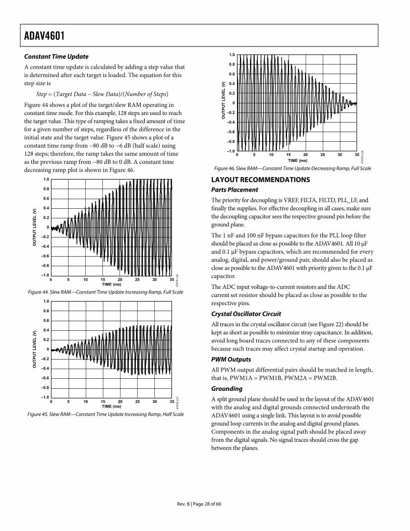
Constant Time Update
A constant time update is calculated by adding a step value that is determined after each target is loaded. The equation for this step size is
Step = (Target Data − Slew Data)/(Number of Steps)
Figure 44 shows a plot of the target/slew RAM operating in constant time mode. For this example, 128 steps are used to reach the target value. This type of ramping takes a fixed amount of time for a given number of steps, regardless of the difference in the initial state and the target value. Figure 45 shows a plot of a constant time ramp from −80 dB to −6 dB (half scale) using 128 steps; therefore, the ramp takes the same amount of time as the previous ramp from −80 dB to 0 dB. A constant time decreasing ramp plot is shown in Figure 46.
0
Figure 46. Slew RAM—Constant Time Update Decreasing Ramp, Full Scale
0707
0-11
6
TIME (ms)
OU
TPU
T LE
VEL
(V)
1.0
0.8
0.6
0.4
0.2
0
–0.6
–0.4
–0.2
–0.8
–1.03525155 20100 3
LAYOUT RECOMMENDATIONS Parts Placement
The priority for decoupling is VREF, FILTA, FILTD, PLL_LF, and finally the supplies. For effective decoupling in all cases, make sure the decoupling capacitor sees the respective ground pin before the ground plane.
0
The 1 nF and 100 nF bypass capacitors for the PLL loop filter should be placed as close as possible to the ADAV4601. All 10 μF and 0.1 μF bypass capacitors, which are recommended for every analog, digital, and power/ground pair, should also be placed as close as possible to the ADAV4601 with priority given to the 0.1 μF capacitor.
The ADC input voltage-to-current resistors and the ADC current set resistor should be placed as close as possible to the respective pins.
Figure 44. Slew RAM—Constant Time Update Increasing Ramp, Full Scale
0707
0-11
7
TIME (ms)
OU
TPU
T LE
VEL
(V)
1.0
0.8
0.6
0.4
0.2
0
–0.6
–0.4
–0.2
–0.8
–1.03525155 20100
Crystal Oscillator Circuit
All traces in the crystal oscillator circuit (see Figure 22) should be kept as short as possible to minimize stray capacitance. In addition, avoid long board traces connected to any of these components because such traces may affect crystal startup and operation.
PWM Outputs
All PWM output differential pairs should be matched in length, that is, PWM1A = PWM1B, PWM2A = PWM2B.
Grounding
30
A split ground plane should be used in the layout of the ADAV4601 with the analog and digital grounds connected underneath the ADAV4601 using a single link. This layout is to avoid possible ground loop currents in the analog and digital ground planes. Components in the analog signal path should be placed away from the digital signals. No signal traces should cross the gap between the planes.
Figure 45. Slew RAM—Constant Time Update Increasing Ramp, Half Scale

ADAV4601
Rev. B | Page 29 of 60
TYPICAL APPLICATION DIAGRAM
ADAV4601
AG
ND
AG
ND
AG
ND
AG
ND
AG
ND
DG
ND
DG
ND
DG
ND
DG
ND
DG
ND
OD
GN
D
BCLK0LRCLK0BCLK1LRCLK1BCLK2LRCLK2SDIN0SDIN1SDIN2SDIN3SDO0
TO A
UD
IO C
ON
TRO
LLER
+
10µF
10nFAUXOUT1L AUXOUT1L
+
10µF
10nFAUXOUT1R AUXOUT1R
+
100µFHPOUT1L HPOUT1L
+
100µFHPOUT1R HPOUT1R
PWM1A PWM1APWM1B PWM1BPWM2A PWM2APWM2B PWM2BPWM3A PWM3APWM3B PWM3BPWM4A PWM4APWM4B PWM4B
PWM_READY PWM_READY
SPDIF_OUT SPDIF_OUT
MCLK_OUT MCLK_OUT
+
10µF
10nFAUXOUT3L AUXOUT3L
+
10µF
10nFAUXOUT4R AUXOUT4R
XIN
XOUT
C1
C2
MUTEMUTE
SPDIF_IN6SPDIF_IN6SPDIF_IN5SPDIF_IN5SPDIF_IN4SPDIF_IN4SPDIF_IN3SPDIF_IN3SPDIF_IN2SPDIF_IN2SPDIF_IN1SPDIF_IN1
RESET
AD0SCLSDA
ICCONTROLLER
MCLKICLOCK
RESETCIRCUITRY
AUXIN1RAUXIN1R20kΩ
+
10µF
AUXIN1LAUXIN1L20kΩ
+
10µF
FILT
D
+
0.1µ
F
10µF
FILT
A
+
0.1µ
F
47µF
VREF
+
0.1µ
F
47µF
ISET
20kΩ
PLL_
LF
2kΩ
1nF 100nF
AVDD (PIN 53)
AVD
D(P
IN 4
)
AVD
D(P
IN 5
3)
+10µF
AVD
D(P
IN 5
9)0.
1µF
+10µF+10
µF
0.1µ
F
1nF
AVD
D(P
IN 6
8)0.
1µF
AVD
D(P
IN 7
1)0.
1µF
0.1µ
F
3.3V
DVD
D
DVD
D
0.1µ
F
0.1µ
F
+10µF
1.8V
0.1µF
+
10µF
3.3V
OD
VDD
0707
0-10
7
Figure 47. Typical Application Circuit

ADAV4601
Rev. B | Page 30 of 60
0x0100 0x0102 0x0105 0x0106 0x0107 0x0108
0x010A
0x010A0x0109
0x012C0x012D0x012E
0x010B
0x010C0x010D0x010E0x010F
0x01100x01110x01120x0113
0x01140x0115
0x0116
0x0117
0x0121
0x0121
0x0100 0x0102 0x0118 0x0120 0x011A0x011B0x011C0x011D
0x011E0x011F
0x0121
0x0101 0x0103 0x0121
0x0101 0x0103 0x0121
0x0101 0x0121
0x0123
0x0103
0x0124
0x0122
LIP
SYN
C
TRIM
AUXOUTL1
AUXOUTR1
HPOUTL1/AUXOUTL4
HPOUTR1/AUXOUTR4
HP
MU
XA
UX
OU
T1M
UX
SPD
IF M
UX
SDO
0 M
UX
TRIM
TRIM
7 B
AN
D E
QM
UTE
MU
TEM
UTE
LOU
DN
ESS
BA
LAN
CE
VOLU
ME
MU
TE
BEEPER
MA
IN M
UX
TRIM
AVC
7 B
AN
D E
Q
LOU
DN
ESS
CR
OSS
OVE
R
CR
OSS
OVE
RTR
IM
8 B
AN
D E
Q
BA
LAN
CE
VO
LUM
E C
ON
TRO
L
LIM
ITER
+
MU
TEM
UTE
PWM1 (LHIGH)/AUXOUT3L
PWM2 (RHIGH)/AUXOUT3R
SPDIF OUTR (SDOR1)
SPDIF OUTL (SDOL1)
PWM3 (LLOW)
PWM4 (RLOW)
+
SDOL0
SDOR0
AUXINL1AUXINR1
TRIM
(L +
R)/2
LPF SUBCHANNEL
TO INPUTMUXES
SUBCHANNEL
SDIN0SDIN1
SPA
TIA
LIZE
R
CR
OSS
OVE
RTR
IM
DYN
AM
ICB
ASS
BA
LAN
CE
LIM
ITER
0x0126
SDIN3/SRC2CHANNEL C
SRC1
SRC2CHANNEL A
SR
C D
ELA
Y
0x0127
0x0127
0x0127
0x0127
SR
C1
MU
TESR
C2
MU
TE
SR
C1
DE-
EMPH
AS
ISS
RC
2D
E-EM
PHA
SIS
SDIN2/SRC2CHANNEL B
0707
0-10
8
Figure 48. Default Audio Processing Flow

ADAV4601
Rev. B | Page 31 of 60
AUDIO FLOW CONTROL REGISTERS DETAILED REGISTER DESCRIPTIONS Address 0x0100 Mux Select 1 Register (Default: 0x0000)
Table 15. Bit No. Bit Name Description Default Bits[15:12] Main source mux Source for main channel. 0000 0x0 = reserved 0x1 = ADC1 0x2 = reserved 0x3 = SDIN0 0x4 = SDIN1 0x5 = SDIN2/SRC2 Channel B 0x6 = SDIN3/SRC2 Channel C 0x7 = SRC1 0x8 = SRC2 Channel A 0x9 = reserved 0xA = reserved Bits[11:8] Reserved Always write as 0 if writing to this register. 0000 Bits[7:4] Headphone 1/AUXOUT4 output Source for the Headphone 1/AUXOUT4 output. 0000 0x0 = reserved 0x1 = ADC1 0x2 = reserved 0x3 = SDIN0 0x4 = SDIN1 0x5 = SDIN2/SRC2 Channel B 0x6 = SDIN3/SRC2 Channel C 0x7 = SRC1 0x8 = SRC2 Channel A 0x9 = reserved 0xA = reserved 0xB = reserved 0xC = delayed main input 0xD = main input after loudness 0xE = subchannel Bits[3:0] AUXOUT3 output mux Source for the AUXOUT3 output. 0000 0x0 = reserved 0x1 = ADC1 0x2 = reserved 0x3 = SDIN0 0x4 = SDIN1 0x5 = SDIN2/SRC2 Channel B 0x6 = SDIN3/SRC2 Channel C 0x7 = SRC1 0x8 = SRC2 Channel A 0x9 = reserved 0xA = reserved 0xB = reserved 0xC = delayed main input 0xD = main input after loudness 0xE = subchannel

ADAV4601
Rev. B | Page 32 of 60
Address 0x0101 Mux Select 2 Register (Default: 0x0000)
Table 16. Bit No. Bit Name Description Default Bits[15:12] SDO0 output Source for the SDO0 output channel. 0000 0x0 = reserved 0x1 = ADC1 0x2 = reserved 0x3 = SDIN0 0x4 = SDIN1 0x5 = SDIN2/SRC2 Channel B 0x6 = SDIN3/SRC2 Channel C 0x7 = SRC1 0x8 = SRC2 Channel A 0x9 = reserved 0xA = reserved 0xB = reserved 0xC = delayed main input 0xD = main input after loudness 0xE = subchannel Bits[11:8] SPDIF output Source for the SPDIF output. 0000 0x0 = reserved 0x1 = ADC1 0x2 = reserved 0x3 = SDIN0 0x4 = SDIN1 0x5 = SDIN2/SRC2 Channel B 0x6 = SDIN3/SRC2 Channel C 0x7 = SRC1 0x8 = SRC2 Channel A 0x9 = reserved 0xA = reserved 0xB = reserved 0xC = delayed main input 0xD = main input after loudness 0xE = subchannel Bits[7:4] AUXOUT1 output Source for the AUXOUT1 output. 0000 0x0 = reserved 0x1 = ADC1 0x2 = reserved 0x3 = SDIN0 0x4 = SDIN1 0x5 = SDIN2/SRC2 Channel B 0x6 = SDIN3/SRC2 Channel C 0x7 = SRC1 0x8 = SRC2 Channel A 0x9 = reserved 0xA = reserved 0xB = reserved 0xC = delayed main input 0xD = main input after loudness 0xE = subchannel Bits[3:0] Reserved Always write as 0 if writing to this register. 0000

ADAV4601
Rev. B | Page 33 of 60
Address 0x0102 Main and Headphone 1/AUXOUT4 Input Trim Register (Default: 0x0E0E)
Table 17. Bit No. Bit Name Description Default Bits[15:14] Reserved Always write as 0 if writing to this register. 00 Bits[13:8] Main input trim These register bits are used to gain or attenuate the input to the main channel
processing path from −14 dB to +14 dB in +1 dB steps. 001110
0x00 = +14 dB 0x01 = +13 dB … 0x07 = +7 dB … 0x0E = 0 dB … 0x15 = −7 dB 0x1B = −13 dB 0x1C = −14 dB Bits[7:6] Reserved Always write as 0 if writing to this register. 00 Bits[5:0] Headphone 1/AUXOUT4 input trim These register bits are used to gain or attenuate the input to the Headphone 1/
AUXOUT4 channel processing path from −14 dB to +14 dB in +1 dB steps. 001110
0x00 = +14 dB 0x01 = +13 dB … 0x07 = +7 dB … 0x0E = 0 dB … 0x15 = −7 dB … 0x1B = −13 dB 0x1C = −14 dB
Address 0x0103 SDO0/AUXOUT3 and SPDIF Input Trim Register (Default: 0x0E0E)
Table 18. Bit No. Bit Name Description Default Bits[15:14] Reserved Always write as 0 if writing to this register. 00 Bits[13:8] SDO0/AUXOUT3 input trim These register bits are used to gain or attenuate the input to the SDO0 and the
AUXOUT3 processing path from −14 dB to +14 dB in +1 dB steps. 001110
0x00 = +14 dB 0x01 = +13 dB … 0x07 = +7 dB … 0x0E = 0 dB … 0x15 = −7 dB 0x1B = −13 dB 0x1C = −14 dB Bits[7:6] Reserved Always write as 0 if writing to this register. 00

ADAV4601
Rev. B | Page 34 of 60
Bit No. Bit Name Description Default Bits[5:0] SPDIF input trim These register bits are used to gain or attenuate the input to the SPDIF processing
path from −14 dB to +14 dB in +1 dB steps. 001110
0x00 = +14 dB 0x01 = +13 dB … 0x07 = +7 dB … 0x0E = 0 dB … 0x15 = −7 dB … 0x1B = −13 dB 0x1C = −14 dB
Address 0x0104 AUXOUT1 Input Trim Register (Default: 0x0E0E)
Table 19. Bit No. Bit Name Description Default Bits[15:14] Reserved Always write as 0 if writing to this register. 00 Bits[13:8] AUXOUT1 input trim These register bits are used to gain or attenuate the input to the AUXOUT1
channel processing path from −14 dB to +14 dB in +1 dB steps. 001110
0x00 = +14 dB 0x01 = +13 dB … 0x07 = +7 dB … 0x0E = 0 dB … 0x15 = −7 dB 0x1B = −13 dB 0x1C = −14 dB Bits[7:0] Reserved Always write as 0 if writing to this register. 00000000
Address 0x0105 Main Delay Register (Default: 0x0000)
Table 20. Bit No. Bit Name Description Default Bits[15:13] Reserved Always write as 0 if writing to this register. 000 Bits[12:0] Main delay These register bits are used to specify the lip synchronization delay for the main channel. 0000000000000 0x0000 = 20.83 μs (1 sample delay at 48 kHz) 0x0001 = 20.83 μs (1 sample delay) 0x0002 = 41.66 μs (2 sample delay) … 0x1C20 = 150 ms (7200 sample delay)

ADAV4601
Rev. B | Page 35 of 60
Address 0x0106 Automatic Volume Control (Default: 0x350C)
Table 21. Bit No. Bit Name Description Default Bits[15:12] AVC maximum gain Used to control the maximum gain in the range of 0 dB to 15 dB. This is the maximum gain
that can be applied to the input signal to reach the desired output level. 0011
0x0 = 15 dB 0x1 = 14 dB 0x2 = 13 dB 0x3 = 12 dB 0x4 = 11 dB 0x5 = 10 dB ... 0xF = 0 dB Bits[11:8] AVC decay time Used to control the decay time in the range of 20 ms to 12 sec. The decay time
corresponds to the time required for the output to reach the desired level. 0101
0x0 = 20 ms 0x1 = 100 ms 0x2 = 200 ms 0x3 = 500 ms 0x4 = 1 sec 0x5 = 2 sec 0x6 = 3 sec 0x7 = 4 sec 0x8 = 5 sec 0x9 = 6 sec 0xA = 7 sec 0xB = 8 sec 0xC = 9 sec 0xD = 10 sec 0xE = 11 sec 0xF = 12 sec Bits[7:4] AVC maximum attenuation Used to control the maximum attenuation in the range of −18 dB to −3 dB in
+1 dB steps. This is the maximum attenuation that can be applied to the input signal to reach the desired output level.
0000
0x0 = −18 dB 0x1 = −17 dB … 0xE = −4 dB 0xF = −3 dB Bits[3:0] AVC output level Used to control the required output level of the AVC block in the range of −3 dBFS to
−18 dBFS in −1 dB steps. If the input signal is greater than the output level that has been set by these bits, the gain is automatically reduced.
1100
0x0 = −18 dBFS 0x1 = −17 dBFS … 0xC = −6 dBFS 0xD = −5 dBFS 0xE = −4 dBFS 0xF = −3 dBFS

ADAV4601
Rev. B | Page 36 of 60
Address 0x0107 Main Sever Band EQ Control Register (Default: 0x0018)
Table 22. Bit No. Bit Name Description Default Bits[15:11] Reserved Always write as 0 if writing to this register. 00000 Bits[10:8] Main EQ band These register bits control the frequency band of the equalizer. 000 0x0 = 120 Hz 0x1 = 200 Hz 0x2 = 500 Hz 0x3 = 1200 Hz 0x4 = 3000 Hz 0x5 = 7500 Hz 0x6 = 12,000 Hz Bits[7:6] Reserved Always write as 0 if writing to this register. 00 Bits[5:0] Main EQ gain These register bits are used to control the required gain of the equalizer. The gain of the equalizer
is changed in 0.5 dB steps. 011000
0x00 = +12 dB 0x01 = +11.5 dB … 0x0A = +7 dB … 0x18 = 0 dB … 0x26 = −7 dB … 0x2F = −11.5 dB 0x30 = −12 dB
Address 0x0108 Main Channel Loudness Register (Default: 0x0000)
Table 23. Bit No. Bit Name Description Default Bits[15:7] Reserved Always write as 0 if writing to this register. 000000000 Bits[6:5] Cutoff frequency These register bits are used to control the cutoff frequency of the loudness. 00 00b – 10 Hz 01b – 30 Hz 10b – 50 Hz 11b – 70 Hz Bits[4:0] Loudness level These register bits are used to control the required level of loudness. 00000 0x00 = 0 dB 0x01 = +1 dB … 0x0E = +14 dB 0x0F = +15 dB

ADAV4601
Rev. B | Page 37 of 60
Address 0x0109 Crossover Register (Default: 0x0505)
Table 24. Bit No. Bit Name Description Default Bits[15:14] Reserved Always write as 0 if writing to this register. 00 Bits[13:8] Low crossover frequency The low crossover frequency is the cutoff frequency of the crossover low-pass
filter. This means that only the frequencies under this frequency are sent to the woofer output. The frequency changes in 10 Hz steps.
000101
0x00 = 50 Hz 0x01 = 60 Hz 0x02 = 70 Hz 0x03 = 80 Hz 0x04 = 90 Hz 0x05 = 100 Hz 0x06 = 110 Hz … 0x2D = 500 Hz 0x2E = 510 Hz Bits[7:6] Reserved Always write as 0 if writing to this register. 00 Bits[5:0] High crossover frequency The high crossover frequency is the cutoff frequency of the crossover high-pass
filter. This means that only the frequencies above this frequency are sent to the tweeter output.
000101
0x00 = 50 Hz 0x01 = 60 Hz 0x02 = 70 Hz 0x03 = 80 Hz 0x04 = 90 Hz 0x05 = 100 Hz 0x06 = 110 Hz ... 0x3B = 640 Hz 0x3C = 650 Hz
Address 0x010A Crossover Trim Register (Default: 0x0E0E)
Table 25. Bit No. Bit Name Description Default Bits[15:14] Reserved Always write as 0 if writing to this register. 00 Bits[13:8] Tweeter trim These register bits are used to gain or attenuate the input to the tweeter outputs from
−14 dB to +14 dB in +1 dB steps. 001110
0x00 = +14 dB 0x01 = +13 dB … 0x07 = +7 dB … 0x0E = 0 dB … 0x15 = −7 dB … 0x1B = −13 dB 0x1C = −14 dB Bits[7:6] Reserved Always write as 0 if writing to this register. 00

ADAV4601
Rev. B | Page 38 of 60
Bit No. Bit Name Description Default Bits[5:0] Woofer trim These register bits are used to gain or attenuate the input to the woofer outputs from
−14 dB to +14 dB in +1 dB steps. 001110
0x00 = +14 dB 0x01 = +13 dB … 0x07 = +7 dB … 0x0E = 0 dB … 0x15 = −7 dB … 0x1B = −13 dB 0x1C = −14 dB
Address 0x010B ADI Bass Control Register (Default: 0x0062)
Table 26. Bit No. Bit Name Description Default Bits[15:9] Reserved Always write as 0 if writing to this register. 0000000 Bits[8:4] Boost value The boost ranges from 0 dB to 31 dB, and it controls the maximum dynamic gain applied to
the algorithm. 00110
0x00 = 0 dB 0x01 = 1 dB 0x02 = 2 dB 0x03 = 3 dB 0x04 = 4 dB 0x05 = 5 dB 0x06 = 6 dB 0x07 = 7 dB … 0x1E = 30 dB 0x1F = 31 dB Bits[3:0] Boost frequency The boost frequency ranges from 20 Hz to 320 Hz, and it designates the center frequency
for the boosting filter. The frequency is increased in 20 Hz steps. 0010
0x0 = 20 Hz 0x1 = 40 Hz 0x2 = 60 Hz 0x3 = 80 Hz … 0xE = 300 Hz 0xF = 320 Hz

ADAV4601
Rev. B | Page 39 of 60
Address 0x010C and Address 0x010D Tweeter Left Balance Control Registers (Default: 0x0080, 0x0000)
These two registers (0x010C and 0x010D) control the balance for the left tweeter output.
The balance control words are 28-bit words in twos complement and a 5.23 format. This means there are five bits to the left of the decimal point of which the most significant bit is the sign bit.
To simplify updating the tweeter left balance control, the I2C address pointer auto-increments when writing and reading. This means that the balance control register can be updated in a single I2C block write. Therefore, it is recommended that the tweeter left balance control be updated using the following I2C write format:
<dev addr><010C><32-bit data transfer>
Note that the tweeter left balance control is a 32-bit parameter; therefore, both Register 0x010C and Register 0x010D must be written to. Writing anything less than the 32 bits to these registers does not update the parameter.
Table 27. Bit No. Bit Name Description Default Bits[15:12] Reserved Always write as 0 if writing to this register. 0000 Bits[11:0] Tweeter left balance control register[27:0] 0x010C Bits[11:0] = tweeter left balance control register[27:16] 000010000000 Bits[15:0] Tweeter left balance control register[27:0] 0x010D Bits[15:0] = tweeter left balance control register[15:0] 0000000000000000
Address 0x010E and Address 0x010F Tweeter Right Balance Control Registers (Default: 0x0080, 0x0000)
These two registers (0x010E and 0x010F) control the balance for the right tweeter output.
The balance control words are 28-bit words in twos complement and a 5.23 format. This means there are five bits to the left of the decimal point of which the most significant bit is the sign bit.
Table 28. Bit No. Bit Name Description Default Bits[15:12] Reserved Always write as 0 if writing to this register. 0000 Bits[11:0] Tweeter right balance control register[27:0] 0x010E Bits[11:0] = tweeter right balance control register[27:16] 000010000000 Bits[15:0] Tweeter right balance control register[27:0] 0x010F Bits[15:0] = tweeter right balance control register[15:0] 0000000000000000
Address 0x0110 and Address 0x0111 Woofer Left Balance Control Registers (Default: 0x0080, 0x0000)
These two registers control the balance for the left woofer output.
The balance control words are 28-bit words in twos complement and a 5.23 format. This means there are five bits to the left of the decimal point of which the most significant bit is the sign bit.
Table 29. Bit No. Bit Name Description Default Bits[15:12] Reserved Always write as 0 if writing to this register. 0000 Bits[11:0] Woofer left balance control register[27:0] 0x0110 Bits[11:0] = woofer left balance control register[27:16] 000010000000 Bits[15:0] Woofer left balance control register[27:0] 0x0111 Bits[15:0] = woofer left balance control register[15:0] 0000000000000000

ADAV4601
Rev. B | Page 40 of 60
Address 0x0112 and Address 0x0113 Woofer Right Balance Control Registers (Default: 0x0080, 0x0000)
These two registers control the balance for the right tweeter output.
The balance control words are 28-bit words in twos complement and a 5.23 format. This means there are five bits to the left of the decimal point of which the most significant bit is the sign bit.
Table 30. Bit No. Bit Name Description Default Bits[15:12] Reserved Always write as 0 if writing to this register. 0000 Bits[11:0] Woofer right balance control register[27:0] 0x0112 Bits[11:0] = woofer right balance control register[27:16] 000010000000 Bits[15:0] Woofer right balance control register[27:0] 0x0113 Bits[15:0] = woofer right balance control register[15:0] 0000000000000000
Address 0x0114 and Address 0x0115 Main Volume Control Registers (Default: 0x0080, 0x0000)
These two registers control the volume for the main channel output.
The volume control words are 28-bit words in twos complement and a 5.23 format. This means there are five bits to the left of the decimal point of which the most significant bit is the sign bit.
Table 31. Bit No. Bit Name Description Default Bits[15:12] Reserved Always write as 0 if writing to this register. 0000 Bits[11:0] Woofer right balance control register[27:0] 0x0114 Bits[11:0] = main volume Bits[27:16] 000010000000 Bits[15:0] Woofer right balance control register[27:0] 0x0115 Bits[15:0] = main volume Bits[15:0] 0000000000000000
Address 0x0116 Tweeter Peak Limiter Control Register (Default: 0x0F00)
This register controls the peak limiter for the main output tweeter.
Table 32. Bit No. Bit Name Description Default Bits[15:13] Reserved Always write as 0 if writing to this register. 000 Bits[12:8] Post gain These register bits control the post gain in the range of +15 dB to −15 dB in +1 dB steps. 01111 0x00 = +15 dB 0x01 = +14 dB … 0x08 = +7 dB … 0x0F = +0 dB … 0x16 = −7 dB … 0x1D = −14 dB 0x1E = −15 dB Bits[7:5] Hold time These register bits control the hold time for the limiter, which is the time in ms that the limiter
holds the attenuated level after the current input to the limiter function falls below the limiter threshold.
000
0x0 = 0 ms 0x1 = 10 ms 0x2 = 20 ms 0x3 = 30 ms 0x4 = 40 ms 0x5 = 50 ms 0x6 = 60 ms 0x7 = 70 ms

ADAV4601
Rev. B | Page 41 of 60
Bit No. Bit Name Description Default Bits[4:0] Decay time These register bits control the decay time for the limiter in the range of 10 dB/s to 320 dB/s in
10 dB/s steps. 00000
0x00 = 10 dB/s (~870 ms) 0x01 = 20 dB/s (~435 ms) 0x02 = 30 dB/s (~289 ms) 0x03 = 40 dB/s (~217 ms) 0x04 = 50 dB/s (~173 ms) 0x05 = 60 dB/s (~144 ms) 0x06 = 70 dB/s (~124 ms) 0x07 = 80 dB/s (~108 ms) 0x08 = 90 dB/s (~96 ms) 0x09 = 100 dB/s (~86 ms) 0x0A = 110 dB/s (~78 ms) 0x0B = 120 dB/s (~72 ms) 0x0C = 130 dB/s (~66 ms) 0x0D = 140 dB/s (~62 ms) 0x0E = 150 dB/s (~57 ms) 0x0F = 160 dB/s (~54 ms) 0x10 = 170 dB/s (~51 ms) 0x11 = 180 dB/s (~48 ms) 0x12 = 190 dB/s (~45 ms) 0x13 = 200 dB/s (~43 ms) 0x14 = 210 dB/s (~41 ms) 0x15 = 220 dB/s (~39 ms) 0x16 = 230 dB/s (~37 ms) 0x17 = 240 dB/s (~36 ms) 0x18 = 250 dB/s (~34 ms) 0x19 = 260 dB/s (~33 ms) 0x1A = 270 dB/s (~32 ms) 0x1B = 280 dB/s (~31 ms) 0x1C = 290 dB/s (~29 ms) 0x1D = 300 dB/s (~28 ms) 0x1E = 310 dB/s (~28 ms) 0x1F = 320 dB/s (~27 ms)
Address 0x0117 Woofer Peak Limiter Control Register (Default: 0x0F00)
Table 33. Bit No. Bit Name Description Default Bits[15:13] Reserved Always write as 0 if writing to this register. 000 Bits[12:8] Post gain These register bits control the post gain in the range of +15 dB to −15 dB in +1 dB steps. 01111 0x00 = +15 dB 0x01 = +14 dB … 0x08 = +7 dB … 0x0F = 0 dB … 0x16 = −7 dB … 0x1D = −14 dB 0x1E = −15 dB

ADAV4601
Rev. B | Page 42 of 60
Bit No. Bit Name Description Default Bits[7:5] Hold time These register bits control the hold time for the limiter, which is the time in ms that the limiter
holds the attenuated level after the current input to the limiter function falls below the limiter threshold.
000
0x0 = 0 ms 0x1 = 10 ms 0x2 = 20 ms 0x3 = 30 ms 0x4 = 40 ms 0x5 = 50 ms 0x6 = 60 ms 0x7 = 70 ms Bits[4:0] Decay time These register bits control the decay time for the limiter in the range of 10 dB/s to 320 dB/s in
10 dB/s steps. 0000
0x00 = 10 dB/s (~870 ms) 0x01 = 20 dB/s (~435 ms) 0x02 = 30 dB/s (~289 ms) 0x03 = 40 dB/s (~217 ms) 0x04 = 50 dB/s (~173 ms) 0x05 = 60 dB/s (~144 ms) 0x06 = 70 dB/s (~124 ms) 0x07 = 80 dB/s (~108 ms) 0x08 = 90 dB/s (~96 ms) 0x09 = 100 dB/s (~86 ms) 0x0A = 110 dB/s (~78 ms) 0x0B = 120 dB/s (~72 ms) 0x0C = 130 dB/s (~66 ms) 0x0D = 140 dB/s (~62 ms) 0x0E = 150 dB/s (~57 ms) 0x0F = 160 dB/s (~54 ms) 0x10 = 170 dB/s (~51 ms) 0x11 = 180 dB/s (~48 ms) 0x12 = 190 dB/s (~45 ms) 0x13 = 200 dB/s (~43 ms) 0x14 = 210 dB/s (~41 ms) 0x15 = 220 dB/s (~39 ms) 0x16 = 230 dB/s (~37 ms) 0x17 = 240 dB/s (~36 ms) 0x18 = 250 dB/s (~34 ms) 0x19 = 260 dB/s (~33 ms) 0x1A = 270 dB/s (~32 ms) 0x1B = 280 dB/s (~31 ms) 0x1C = 290 dB/s (~29 ms) 0x1D = 300 dB/s (~28 ms) 0x1E = 310 dB/s (~28 ms) 0x1F = 320 dB/s (~27 ms)

ADAV4601
Rev. B | Page 43 of 60
Address 0x0118 Headphone 1/AUXOUT4 Seven Band EQ Control Register (Default: 0x0018)
Table 34. Bit No. Bit Name Description Default Bits[15:11] Reserved Always write as 0 if writing to this register. 00000 Bits[10:8] Headphone 1/
AUXOUT4 EQ band These register bits control the frequency band of the equalizer. 000
0x0 = 120 Hz 0x1 = 200 Hz 0x2 = 500 Hz 0x3 = 1200 Hz 0x4 = 3000 Hz 0x5 = 7500 Hz 0x6 = 12000 Hz Bits[7:6] Reserved Always write as 0 if writing to this register. 00 Bits[5:0] Headphone 1/
AUXOUT4 EQ gain These register bits are used to control the required gain of the equalizer. The gain of the equalizer is changed in 0.5 dB steps.
001110
0x00 = +12 dB 0x01 = +11.5 dB … 0x0A = +7 dB … 0x18 = 0 dB … 0x26 = −7 dB … 0x2F = −11.5 dB 0x30 = −12 dB
Address 0x011A and Address 0x011B Headphone 1/AUXOUT4 Left Balance Control Registers (Default: 0x0080, 0x0000)
These two registers control the balance for the Left Headphone 1 and AUXOUT 4 output.
The balance control words are 28-bit words in twos complement and a 5.23 format. This means there are five bits to the left of the decimal point of which the most significant bit is the sign bit.
Table 35. Bit No. Bit Name Description Default Bits[15:12] Reserved Always write as 0 if writing to this register. 0000 Bits[11:0] Woofer left balance
control register[27:0] 0x011A Bits[11:0] = Headphone 1/AUXOUT 4 left balance control register[27:16] 000010000000
Bits[15:0] Woofer left balance control register[27:0]
0x011B Bits[15:0] = Headphone 1/AUXOUT 4 left balance control register[15:0] 0000000000000000
Address 0x011C and Address 0x011D Headphone 1/AUXOUT4 Right Balance Control Registers (Default: 0x0080, 0x0000)
These two registers control the balance for the Right Headphone 1 and AUXOUT 4 output.
The balance control words are 28-bit words in twos complement and a 5.23 format. This means there are five bits to the left of the decimal point of which the most significant bit is the sign bit.
Table 36. Bit No. Bit Name Description Default Bits[15:12] Reserved Always write as 0 if writing to this register. 0000 Bits[11:0] Woofer left balance
control register[27:0] 0x011C Bits[11:0] = Headphone 1/AUXOUT 4 right balance control register[27:16]
000010000000
Bits[15:0] Woofer left balance control register[27:0]
0x011D Bits[15:0] = Headphone 1/AUXOUT 4 right balance control register[15:0]
0000000000000000

ADAV4601
Rev. B | Page 44 of 60
Address 0x011E and Address 0x011F Headphone 1/AUXOUT4 Volume Control Registers (Default: 0x0080, 0x0000)
These two registers control the volume for the headphone and AUXOUT4 outputs.
The volume control words are 28-bit words in twos complement and a 5.23 format. This means there are five bits to the left of the decimal point of which the most significant bit is the sign bit.
Table 37. Bit No. Bit Name Description Default Bits[15:12] Reserved Always write as 0 if writing to this register. 0000 Bits[11:0] Headphone 1 volume control[27:0] 0x011E Bits[11:0] = Headphone 1/AUXOUT 4 volume
Bits[27:16] 000010000000
Bits[15:0] Headphone 1 volume control[27:0] 0x011F Bits[15:0] = Headphone 1/AUXOUT 4 volume Bits[15:0]
0000000000000000
Address 0x0120 Headphone 1/AUXOUT4 Channel Loudness Register (Default: 0x0000)
Table 38. Bit No. Bit Name Description Default Bits[15:7] Reserved Always write as 0 if writing to this register. 000000000 Bits[6:5] Cutoff frequency These register bits are used to control the cutoff frequency of the loudness. 00 00b = 10 Hz 01b = 30 Hz 10b = 50 Hz 11b = 70 Hz Bits[4:0] Loudness level These register bits are used to control the required level of loudness. It can be
changed in 1 dB steps. 00000
0x00 = 0 dB 0x01 = 1 dB … 0x0E = 14 dB 0x0F = 15 dB
Address 0x0121 Mute Control Register (Default: 0x0000)
Table 39. Bit No. Bit Name Description Default Bits[15:8] Reserved Always write as 0 if writing to this register. 00000000 Bit[7] Mute tweeter output Mutes the tweeter output. 0 0b = mutes 1b = unmutes Bit[6] Mute woofer output Mutes the woofer output. 0 0b = mutes 1b = unmutes Bit[5] Mute AUXOUT3 output Mutes the AUXOUT3 output. 0 0b = mutes 1b = unmutes Bit[4] Mute HP1/AUXOUT4 output Mutes the Headphone 1 and AUXOUT4 output. 0 0b = mutes 1b = unmutes Bit[3] Mute SDO0 output Mutes the SDO0 output. 0 0b = mutes 1b = unmutes Bit[2] Mute SPDIF output Mutes the SPDIF output. 0 0b = mutes 1b = unmutes

ADAV4601
Rev. B | Page 45 of 60
Bit No. Bit Name Description Default Bit[1] Mute AUXOUT1 output Mutes the AUXOUT1 output. 0 0b = mutes 1b = unmutes Bit[0] Reserved Always write as 0 if writing to this register. 0
Address 0x0122 Audio Flow Control Register (Default: 0x8001)
Table 40. Bit No. Bit Name Description Default Bit[15] Reserved Always write a 1 if writing to this register. 1 Bit[14] Enable AVC When set to 1, it enables the AVC function. 0 0b = disabled 1b = enabled Bit[13] Enable main delay When set to 1, it enables the lip synchronization delay. 0 0b = disabled 1b = enabled Bit[12] Enable main EQ When set to 1, it enables the seven band equalizer. 0 0b = disabled 1b = enabled Bit[11] Enable ADI bass When set to 1, it enables the ADI bass. 0 0b = disabled 1b = enabled Bit[10] Enable main loudness When set to 1, it enables the loudness. 0 0b = disabled 1b = enabled Bit[9] Enable main beeper When set to 1, it leaves only the beeper on the main channel. By default, this register bit
is set to 0, which means the main channel input is added to the beeper. 0
0b = beeper and channel 1b = beeper only Bit[8] Enable main limiter When set to 1, it enables the tweeter and woofer peak limiters. 0 0b = disabled 1b = enabled Bit[7] Enable speaker EQ When set to 1, it enables the eight band speaker equalizer for the tweeter output. 0 0b = disabled 1b = enabled Bit[6] Enable crossover bypass When set to 1, it enables the crossover low-pass and high-pass filters for the main channel. 0 0b = disabled 1b = enabled Bit[5] Tweeter output control When set to 1, the tweeter and woofer outputs are added together and output on
the tweeter output. 0
0b = tweeter only 1b = tweeter and woofer Bit[4] Enable subchannel LPF Used to control the LPF on the subchannel. 0 0b = enabled 1b = disabled Bit[3] Enable HP1 EQ When set to 1, it enables the seven band equalizer for the Headphone 1 channel. 0 0b = disabled 1b = enabled
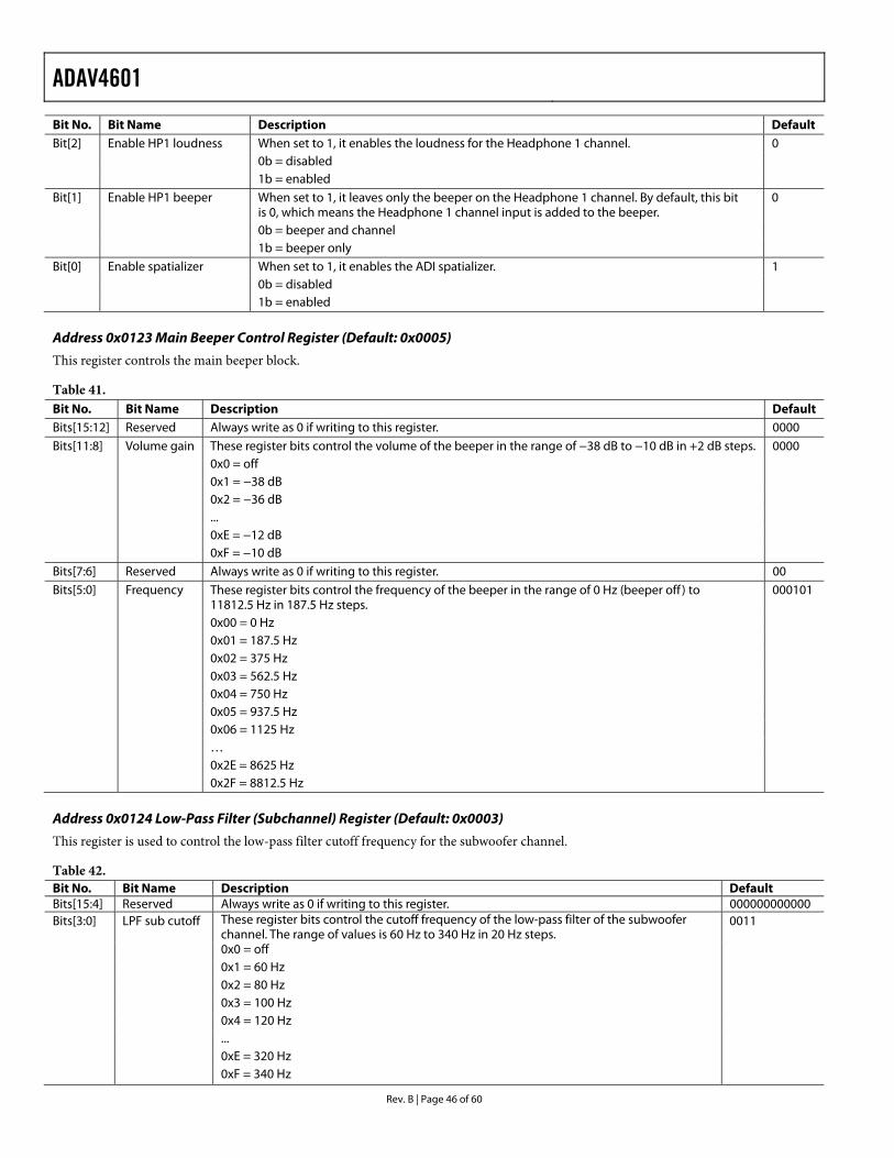
ADAV4601
Rev. B | Page 46 of 60
Bit No. Bit Name Description Default Bit[2] Enable HP1 loudness When set to 1, it enables the loudness for the Headphone 1 channel. 0 0b = disabled 1b = enabled Bit[1] Enable HP1 beeper When set to 1, it leaves only the beeper on the Headphone 1 channel. By default, this bit
is 0, which means the Headphone 1 channel input is added to the beeper. 0
0b = beeper and channel 1b = beeper only Bit[0] Enable spatializer When set to 1, it enables the ADI spatializer. 1 0b = disabled 1b = enabled
Address 0x0123 Main Beeper Control Register (Default: 0x0005)
This register controls the main beeper block.
Table 41. Bit No. Bit Name Description Default Bits[15:12] Reserved Always write as 0 if writing to this register. 0000 Bits[11:8] Volume gain These register bits control the volume of the beeper in the range of −38 dB to −10 dB in +2 dB steps. 0000 0x0 = off 0x1 = −38 dB 0x2 = −36 dB ... 0xE = −12 dB 0xF = −10 dB Bits[7:6] Reserved Always write as 0 if writing to this register. 00 Bits[5:0] Frequency These register bits control the frequency of the beeper in the range of 0 Hz (beeper off ) to
11812.5 Hz in 187.5 Hz steps. 000101
0x00 = 0 Hz 0x01 = 187.5 Hz 0x02 = 375 Hz 0x03 = 562.5 Hz 0x04 = 750 Hz 0x05 = 937.5 Hz 0x06 = 1125 Hz … 0x2E = 8625 Hz 0x2F = 8812.5 Hz
Address 0x0124 Low-Pass Filter (Subchannel) Register (Default: 0x0003)
This register is used to control the low-pass filter cutoff frequency for the subwoofer channel.
Table 42. Bit No. Bit Name Description Default Bits[15:4] Reserved Always write as 0 if writing to this register. 000000000000Bits[3:0] LPF sub cutoff These register bits control the cutoff frequency of the low-pass filter of the subwoofer
channel. The range of values is 60 Hz to 340 Hz in 20 Hz steps. 0011
0x0 = off 0x1 = 60 Hz 0x2 = 80 Hz 0x3 = 100 Hz 0x4 = 120 Hz ... 0xE = 320 Hz 0xF = 340 Hz

ADAV4601
Rev. B | Page 47 of 60
Address 0x0126 SRC Delay Register (Default: 0x0000)
This register is used to set the delay for the SRC channel.
Table 43. Bit No. Bit Name Description Default Bits[15:12] Reserved Always write as 0 if writing to this register. 0000 Bits[11:0] SRC delay The range of values is 20.83 μs to 42 ms in 20.83 μs (1 sample delay) steps. 000000000000 0x000 = 20.83 μs (1 sample delay) 0x001 = 41.66 μs (2 sample delay) ... 0x7E1 = 42 ms (2017 sample delay)
Address 0x0127 SRC Control Register (Default: 0x0030)
This register is used to enable the DSP mute circuit for SRC1 and SRC2. If SRC is enabled and detects an error, it will mute the output of the SRC. It also bypasses the de-emphasis filters of the SRC.
Table 44. Bit No. Bit Name Description Default Bits[15:6] Reserved Always write as 0 if writing to this register. 0000000000 Bit[5] SRC1 de-emphasis filter bypass This bypasses the SRC1 de-emphasis filter. 0 0b = bypass 1b = enabled Bit[4] SRC2 de-emphasis filter bypass This bypasses the SRC2 de-emphasis filter. 0 0b = bypass 1b = enabled Bit[3] SRC1 DSP mute circuit bypass If an error is detected, it mutes the output of SRC1. 0 0b = enabled 1b = disabled Bit[2] SRC2 Channel A DSP mute circuit bypass If an error is detected, it mutes the output of SRC2. 0 0b = enabled 1b = disabled Bit[1] SRC2 Channel B DSP mute circuit bypass If an error is detected, it mutes the output of SRC2. 0 0b = enabled 1b = disabled Bit[0] SRC2 Channel C DSP mute circuit bypass If an error is detected, it mutes the output of SRC2. 0 0b = enabled 1b = disabled

ADAV4601
Rev. B | Page 48 of 60
MAIN CONTROL REGISTERS DETAILED REGISTER DESCRIPTIONS Address 0x0000 Initialization Control Register (Default: 0x0080)
Table 45. Bit No. Bit Name Description Default Bits[15:13] Reserved Always write as 0 if writing to this register. 000 Bit[12] Slew mute When set to 1, all slew parameters ramp to zero. It is recommended to set this
bit to 1 prior to downloading a new program to reduce any risk of pops or clicks on the output.
0
0b = unmuted 1b = muted Bit[11] Reserved Always write as 0 if writing to this register. 0 Bits[10:9] MCLKI frequency select Used to select the MCLKI pin frequency. 00 00b = 512 × frequency sample (FS) (24.576 MHz) 01b = 256 × FS (12.288 MHz) 10b = 128 × FS (6.144 MHz) 11b = 64 × FS (3.072 MHz) Bits[8:7] SRC2 Channel A input select Used to select the source for SRC2 Channel A. 01 00b = SDIN0 01b = SDIN1 10b = SDIN2 11b = SDIN3 Bits[6:5] SRC1 input select Used to select the source for SRC1. 00 00b = SDIN0 01b = SDIN1 10b = SDIN2 11b = SDIN3 Bit[4] SRC2 Channel A enable Used to enable SRC2 Channel A. 0 0b = disabled 1b = enabled Bit[3] SRC1 enable Used to enable SRC1 Channel A. 0 0b = disabled 1b = enabled Bit[2] GSB enable When set to 1, the ADAV4601 enters standby mode. 0 0b = disable standby or not in standby 1b = enable standby or not in standby Bit[1] Audio processor enable Set to 1 to enable the audio processor. 0 0b = disabled 1b = enabled Bit[0] GPU Globally powers up all parts of the device. If read back, it indicates the status of
the global power-up. 0
0b = use power management register 1b = global power-up

ADAV4601
Rev. B | Page 49 of 60
Address 0x0004 Serial Port Control 1 Register (Default: 0x0000)
Table 46. Bit No. Bit Name Description Default Bits[15:13] Reserved Always write as 0 if writing to this register. 000 Bits[12:11] SRC2 serial mode Used to select the format of the data for SRC2. 00 00b = I2S 01b = left-justified 10b = right-justified 11b = not applicable Bits[10:9] SRC2 word width Used to specify the word width of the data. 00 00b = 24 bits 01b = 20 bits 10b = 16 bits 11b = not applicable Bits[8:7] SRC1 serial mode Used to select the format of the data for SRC1. 00 00b = I2S 01b = left-justified 10b = right-justified 11b = not applicable Bits[6:5] SRC1 word width Used to specify the word width of the data. 00 00b = 24 bits 01b = 20 bits 10b = 16 bits 11b = not applicable Bit[4] Sync master slave Used to set master or slave mode for the synchronous input. In slave mode, LRCLK1 and BCLK1
are provided by another source. In master mode, the ADAV4601 provides LRCLK1 and BCLK1. 0
0b = slave 1b = master Bits[3:2] Sync serial mode Used to select the format of the data for the inputs used by the synchronous serial input block. 00 00b = I2S 01b = left-justified 10b = right-justified 11b = not applicable Bits[1:0] Sync word width Used to specify the word width of the data for the synchronous digital inputs. 00 00b = 24 bits 01b = 20 bits 10b = 16 bits 11b = not applicable
Address 0x0005 Analog Power Management 1 Register (Default: 0x8000)
Table 47. Bit No. Bit Name Description Default Bit[15] DAC standby disable Set to 1 after reset, which means all DACs are in normal mode but are still powered down. 1 0b = DACs in low power mode 1b = DACs in normal mode Bit[14] Reserved Always write as 0 if writing to this register. 0 Bit[13] REF BUF Provides the voltage reference for the analog core. 0 1b = block powered up 0b = block powered down Bit[12] Reserved Always write as 0 if writing to this register. 0 Bit[11] Reserved Always write as 0 if writing to this register. 0

ADAV4601
Rev. B | Page 50 of 60
Bit No. Bit Name Description Default Bit[10] ADC1 right Powers on the ADC1 right channel. 0 1b = block powered up 0b = block powered down Bit[9] ADC1 left Powers on the ADC1 left channel. 0 1b = block powered up 0b = block powered down Bit[8:7] Reserved Always write as 0 if writing to this register. 00 Bit[6] AUXDAC3 right Powers on the AUXDAC3 right channel. 0 1b = block powered up 0b = block powered down Bit[5] AUXDAC3 left Powers on the AUXDAC3 left channel. 0 1b = block powered up 0b = block powered down Bit[4] Reserved Always write as 0 if writing to this register. 0 Bit[3] Reserved Always write as 0 if writing to this register. 0 Bit[2] Reserved Always write as 0 if writing to this register. 0 Bit[1] AUXDAC1 right Powers on the AUXDAC1 right channel. 0 1b = block powered up 0b = block powered down Bit[0] AUXDAC1 left Powers on the AUXDAC1 left channel. 0 1b = block powered up 0b = block powered down
Address 0x0006 Analog Power Management 2 Register (Default: 0x0000)
Table 48. Bit No. Bit Name Description Default Bits[15:10] Reserved Always write as 0 if writing to this register. 000000 Bit[9] PLL Powers on the PLL. 0 1b = block powered up 0b = block powered down Bits[8:6] Reserved Always write as 0 if writing to this register. 000 Bit[5] Reserved Always write as 0 if writing to this register. 0 Bit[4] Reserved Always write as 0 if writing to this register. 0 Bit[3] HP1 DAC right Powers on the HP1 DAC right channel. 0 1b = block powered up 0b = block powered down Bit[2] HP1 DAC left Powers on the HP1 DAC left channel. 0 1b = block powered up 0b = block powered down Bit[1] HP1 AMP right Powers on the HP1 AMP right channel. 0 1b = block powered up 0b = block powered down Bit[0] HP1 AMP left Powers on the HP1 AMP left channel. 0 1b = block powered up 0b = block powered down
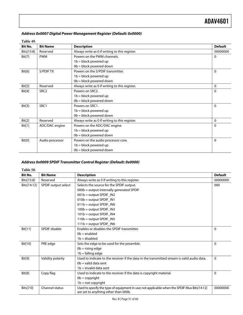
ADAV4601
Rev. B | Page 51 of 60
Address 0x0007 Digital Power Management Register (Default: 0x0000)
Table 49. Bit No. Bit Name Description Default Bits[15:8] Reserved Always write as 0 if writing to this register. 00000000 Bit[7] PWM Powers on the PWM channels. 0 1b = block powered up 0b = block powered down Bit[6] S/PDIF TX Powers on the S/PDIF transmitter. 0 1b = block powered up 0b = block powered down Bit[5] Reserved Always write as 0 if writing to this register. 0 Bit[4] SRC2 Powers on SRC2. 0 1b = block powered up 0b = block powered down Bit[3] SRC1 Powers on SRC1. 0 1b = block powered up 0b = block powered down Bit[2] Reserved Always write as 0 if writing to this register. 0 Bit[1] ADC/DAC engine Powers on the ADC/DAC engine. 0 1b = block powered up 0b = block powered down Bit[0] Audio processor Powers on the audio processor core. 0 1b = block powered up 0b = block powered down
Address 0x0009 SPDIF Transmitter Control Register (Default: 0x0000)
Table 50. Bit No. Bit Name Description Default Bits[15:8] Reserved Always write as 0 if writing to this register. 00000000 Bits[14:12] SPDIF output select Selects the source for the SPDIF output. 000 000b = output internally generated SPDIF 001b = output SPDIF_IN2 010b = output SPDIF_IN1 011b = output SPDIF_IN0 100b = output SPDIF_IN3 101b = output SPDIF_IN4 110b = output SPDIF_IN5 111b = output SPDIF_IN6 Bit[11] SPDIF disable Enables or disables the SPDIF transmitter. 0 0b = enabled 1b = disabled Bit[10] PRE edge Sets the edge to be used for the preamble. 0 0b = rising edge 1b = falling edge Bit[9] Validity polarity Used to indicate to the receiver if the data in the transmitted stream is valid audio data. 0 0b = valid data sent 1b = invalid data sent Bit[8] Copy flag Used to indicate to the receiver if the data is copyright material. 0 0b = copyright 1b = not copyright Bits[7:0] Channel status Used to specify the type of equipment in use; not applicable when the SPDIF Mux Bits[14:12]
are set to anything other than 000b. 00000000

ADAV4601
Rev. B | Page 52 of 60
Address 0x000A Misc Control Register (Default: 0x0800)
Table 51. Bit No. Bit Name Description Default Bit[15] PWM ready flag (read-only) Indicates the current status of the PWM ready pin. When PWM ready is low, the
PWM is not enabled. When PWM ready is high, the PWM is enabled and stable. 0
0b = PWM ready pin low 1b = PWM ready pin high Bit[14] Enable selected PWM channels When enabled, all PWM channels selected by Bits[10:7] can be used. 0 0b = all PWM channels disabled 1b = selected PWM channels enabled Bit[13] MCLK_OUT CLK type select Used to configure the MCLK_OUT pin. 0 0b = crystal frequency on MCLK_OUT 1b = internally generated clocks on MCLK_OUT Bit[12] PWM enable/disable patterns Enables the enable/disable patterns for the PWM block. 0 0b = enable/disable pattern not used 1b = use enable/disable pattern Bit[11] DAC mod offset Adds dc offset to the DAC Σ-Δ modulator to eliminate idle tones. It is recommended
that this bit be disabled before the ADC/DAC engine is powered up in Control Register 0x0007[1].
1
0b = enabled 1b = disabled Bit[10] PWM Enable 4 The PWM outputs are disabled by default, which means that the outputs are
at GND. When this bit is set to 1 and Bit[14] of this register is set to 1, then the PWM Enable 4 channel is enabled.
0
0b = disabled 1b = enabled Bit[9] PWM Enable 3 The PWM outputs are disabled by default, which means that the outputs are
at GND. When this bit is set to 1 and Bit[14] of this register is set to 1, then the PWM Enable 3 channel is enabled.
0
0b = disabled 1b = enabled Bit[8] PWM Enable 2 The PWM outputs are disabled by default, which means that the outputs are
at GND. When this bit is set to 1 and Bit[14] of this register is set to 1, then the PWM Enable 2 channel is enabled.
0
0b = disabled 1b = enabled Bit[7] PWM Enable 1 The PWM outputs are disabled by default, which means that the outputs are
at GND. When this bit is set to 1 and Bit[14] of this register is set to 1, then the PWM Enable 1 channel is enabled.
0
0b = disabled 1b = enabled Bit[6] SRC2 lock (read-only) Set to 1 when the sample rate converter (SRC) locks to the incoming data,
indicating the data is valid. 0
0b = not locked 1b = locked Bit[5] SRC1 lock (read-only) Set to 1 when the sample rate converter (SRC) locks to the incoming data,
indicating the data is valid. 0
0b = not locked 1b = locked Bit[4] MCLK_OUT enable Enables the clock chosen by Bit[13] and Bits[3:1] to be output on the MCLK_OUT pin. 0 0b = MCLK_OUT function disabled 1b = MCLK_OUT function enabled
ADAV4601
Rev. B | Page 53 of 60
Bit No. Bit Name Description Default Bits[3:1] Select internally generated
clock Selects the frequency of the internally generated clock to be output on the MCLK_OUT pin. 000
000b = crystal clock from internal PLL 001b = audio processor clock (122.88 MHz/2560 × FS) 010b = engine clock (49.152 MHz/1024 × FS) 011b = SRC clock/2 (24.576 MHz/512 × FS) 1xxb = modulator clock (6.144 MHz/128 × FS) Bit[0] PLL enable Enables the PLL. 0 0b = PLL bypassed 1b = PLL enabled
Address 0x000B Headphone Control Register (Default: 0x0000)
Table 52. Bit No. Bit Name Description Default Bits[15:8] Reserved Always write as 0 if writing to this register. 00000000 Bit[7] HP1 mute When set to 1, mutes the headphone output immediately without ramping. 0 0b = unmuted 1b = mute Bit[6] HP1 short-circuit protect Enables the short-circuit protection for the headphone amplifier. 0 0b = disabled 1b = enabled Bit[5] HP1 tristate Disables tristating of the headphone amplifier. 0 0b = enabled 1b = disabled Bits[4:0] Headphone 1 gain/attenuation Used to apply analog attenuation to the headphone amplifier. 00000 00000b = 0 dB 00001b = −1.5 dB 00010b = −3 dB … 11101b = −43.5 dB 11110b = −45 dB 11111b = +1.5 dB
Address 0x000C Serial Port Control 2 Register (Default: 0x8004)
It should be noted that SDIN3, LRCLK0, BCLK0, LRCLK1, BCLK1, LRCLK2, and BCLK2 can also be used as SPDIF_IN0, SPDIF_IN1, SPDIF_IN2, SPDIF_IN3, SPDIF_IN4, SPDIF_IN5, and SPDIF_IN6.
Table 53. Bit No. Bit Name Description Default Bits[15:14] SCR2 clock select Used to select the serial clocks used for the input to SRC2. 10 00b = uses LRCLK0 and BCLK0 01b = uses LRCLK1 and BCLK1 10b = uses LRCLK2 and BCLK2 11b = reserved Bits[13:12] SRC1 clock select Used to select the serial clocks used for the input to SRC1. 00 00b = uses LRCLK0 and BCLK0 01b = uses LRCLK1 and BCLK1 10b = uses LRCLK2 and BCLK2 11b = reserved Bit[11] Reserved Always write as 0 if writing to this register. 0

ADAV4601
Rev. B | Page 54 of 60
Bit No. Bit Name Description Default Bit[10] Digout Enable 1 Used to change the function of the PWM1A and PWM1B pins to additional serial
digital outputs, SDO2 and SDO3. 0
0b = PWM1A and PWM1B in normal operation 1b = PWM1A and PWM1B used as SDO2 and SDO3 Bit[9] Digout Enable 2 Used to change the function of SPDIF output to serial digital output SDO1. 0 0b = SPDIF output normal operation 1b = SPDIF output used as SDO1 Bits[8:7] BCLK frequency (master) Used to set the BCLK frequency when the synchronous serial port is in master mode. 00 00b = 64 × frequency sample, FS (3.072 MHz) 01b = 128 × FS (6.144 MHz) 10b = 256 × FS (12.288 MHz) 11b = reserved Bits[6:5] Reserved Always write as 0 if writing to this register. 00 Bit[4] Dither enable When set to 1, it performs dithering on the digital output when the word width
is set to 20 bits or 16 bits. This reduces the effect of truncation noise. 0
0b = disabled 1b = enabled Bits[3:2] Synchronous port clock select Used to select the serial clocks used for the synchronous digital inputs. 0 00b = uses LRCLK0 and BCLK0 01b = uses LRCLK1 and BCLK1 10b = uses LRCLK2 and BCLK2 11b = reserved Bit[1] 8-channel time division
multiplexing enable When set to 1, time division multiplexing mode is enabled. 0
0b = disabled 1b = enabled Bit[0] Reserved Always write as 0 if writing to this register. 0
Address 0x0018 Audio Mute Control 1 Register (Default: 0x7F00)
Table 54. Bit No. Bit Name Description Default Bits[15:8] PWM output latency Set the delay from the 50/50 duty-cycle square wave to zero on GND when the output
is muted and Bit[5] is set to 1. 01011111
0x00 = 1.066 ms 0x01 = 2.133 ms … 0x5F = 101.33 ms … 0xFE = 270.93 ms 0xFF = 272 ms Bits[7:6] Reserved Always write as 0 if writing to this register. 00 Bit[5] PWM zero enable Used to specify the final condition of the PWM channels after a mute. 0 0b = PWM not zeroed after audio mute 1b = PWM zeroed after audio mute Bit[4] Mute clear select Mute clear select bit. When the mute pin is used to mute the device, the part can be
unmuted in two ways, depending on the condition of this bit. 0
0b = mute pin rising edge clears mute bit 1b = mute clear gated by clear mute bit Bit[3] Audio mute Used to control the software mute. 0 0b = unmute 1b = mute

ADAV4601
Rev. B | Page 55 of 60
Bit No. Bit Name Description Default Bit[2] Clear mute Set to 1 to unmute the ADAV4601 when the external pin has been used to mute the
part and the mute clear select bit is set. Having performed the required action, this bit automatically resets to 0.
0
0b = no change 1b = clear pin mute Bit[1] Mute status (read-only) Displays the status of the ADAV4601 mute. 0 0b = currently unmuting or unmuted 1b = currently muting or muted Bit[0] Mute flag (read-only) Set to 1 when the ADAV4601 is in mute. 0 0b = unmuted 1b = muted
Address 0x0019 PWM Status Register (Default: 0x0000)
Table 55. Bit No. Bit Name Description Default Bits[15:4] Reserved Always write as 0 if writing to this register. 000000000000 Bit[3] PWM4 status Set when the PWM4 outputs have gone from zero to 50/50 duty cycle. 0 0b = PWM4 disabled 1b = PWM4 enabled Bits[2] PWM3 status Set when the PWM3 outputs have gone from zero to 50/50 duty cycle. 0 0b = PWM3 disabled 1b = PWM3 enabled Bits[1] PWM2 status Set when the PWM2 outputs have gone from zero to 50/50 duty cycle. 0 0b = PWM2 disabled 1b = PWM2 enabled Bit[0] PWM1 status Set when the PWM1 outputs have gone from zero to 50/50 duty cycle. 0 0b = PWM1 disabled 1b = PWM1 enabled
Address 0x001F PWM Control Register (Default: 0x1070)
Table 56. Bit No. Bit Name Description Default Bits[15:14] PWM ready configure 00b = PWM ready forced low 00 01b = PWM ready forced high 10b = PWM ready late 11b = PWM ready early Bit[13] Reserved Always write as 0 if writing to this register. 0 Bit[12] Reserved Always write a 1 if writing to this register 1 Bits[11:7] Reserved Always write as 0 if writing to this register. 00000 Bits[6:4] Reserved Always write a 1 if writing to this register. 111 Bits[3:0] Reserved Always write as 0 if writing to this register. 0000

ADAV4601
Rev. B | Page 56 of 60
Address 0x008A SRC Configuration 3 Register (Default: 0x0032)
Table 57. Bit No. Bit Name Description Default Bits[15:7] Reserved Always write as 0 if writing to this register. 000000000 Bit[6] SRC2 Channel C enable Used to enable Channel C of SRC2. 0 0b = disabled 1b = enabled Bits[5:4] SRC2 Channel C input select Used to select the serial data input for SRC2 Channel C. 11 00b = SDIN0 01b = SDIN1 10b = SDIN2 11b = SDIN3 Bit[3] Reserved Always write as 0 if writing to this register. 0 Bit[2] SRC2C Channel B enable Used to enable Channel B of SRC2. 0 0b = disabled 1b = enabled Bits[1:0] SRC2C Channel B input select Used to select the serial data input for SRC2 Channel B. 10 00b = SDIN0 01b = SDIN1 10b = SDIN2 11b = SDIN3
Address 0x008E SPDIF Transmitter Control 2 Register (Default: 0x002D)
Table 58. Bit No. Bit Name Description Default Bits[15:8] Reserved Always write as 0 if writing to this register. 00000000 Bits[7:4] Channel status sampling frequency Used to set the channel status sampling rate in the SPDIF transmitted
stream; should not change the sample rate but only the status bits. 0010
0x0 = 44.1 kHz 0x2 = 48 kHz 0x3 = 32 kHz Bit[3] SPDIF TX word length field size Selects the maximum SPDIF transmitter word length. 1 0b = 20 bits maximum 1b = 24 bits maximum Bits[2:0] Transmitter word length Used to select how many of the bits set by Bit[3] carry valid data.
If 24-bit maximum 101
0x5 = 24 bits 0x4 = 23 bits 0x2 = 22 bits 0x6 = 21 bits 0x1 = 20 bits If 20-bit maximum 0x5 = 20 bits 0x4 = 19 bits 0x2 = 18 bits 0x6 = 17 bits 0x1 = 16 bits

ADAV4601
Rev. B | Page 57 of 60
Address 0x0200 EEPROM Self Boot Control Register (Default: 0x0000)
Table 59. Bit No. Bit Name Description Default Bits[15] Self-boot enable It initiates a self-boot from the external EEPROM. 0 0b = normal operation 1b = initiates self-boot Bits[14:6] Reserved Always write as 0 if writing to this register. 000000000 Bit[5] Safe load target/slew RAM Initiates a safe load to the target/slew RAM; cleared when safe load completed. 0 0b = finished 1b = safe load request Bit[4] Safe load parameter RAM Initiates a safe load to the parameter RAM; cleared when safe load completed. 0 0b = finished 1b = safe load request Bits[3:0] Reserved Always write as 0 if writing to this register. 0000
Address 0x0316 EEPROM Device Address Register (Default: 0x0050)
Bit No. Bit Name
Table 60. Description Default
Bits[15:7] Reserved Always write as 0 if writing to this register. 000000000 Bits[6:0] EEPROM device address 0x50 = sets external EEPROM address 1010000
Address 0x0317 EEPROM Data Address Register (Default: 0x0000)
Table 61. Bit No. Bit Name Description Default Bits[15:0] EEPROM start address 0x0000 = default address 0000000000000000

ADAV4601
Rev. B | Page 58 of 60
OUTLINE DIMENSIONS
COMPLIANT TO JEDEC STANDARDS MS-026-BEC
1.45 1.40 1.35
0.150.05
0.200.09
0.10COPLANARITY
VIEW AROTATED 90° CCW
SEATINGPLANE
7°3.5°0°
61601
80
20 4121 40
VIEW A
1.60MAX
0.750.600.45
16.2016.00 SQ15.80
14.2014.00 SQ13.80
0.65BSC
LEAD PITCH
0.380.320.22
TOP VIEW(PINS DOWN)
PIN 1
0517
06-A
Figure 49. 80-Lead Low Profile Quad Flat Package [LQFP]
(ST-80-2) Dimensions shown in millimeters
ORDERING GUIDE Model Temperature Range Package Description Package Option ADAV4601BSTZ1 –40°C to +85°C 80-Lead Low Profile Quad Flat Package [LQFP] ST-80-2 EVAL-ADAV4601EBZ1
Evaluation Board 1 Z = RoHS Compliant Part. The ADAV4601 is a Pb-free, environmentally friendly product. It is manufactured using the most up-to-date materials and processes. The
coating on the leads of each device is 100% pure Sn electroplate. The device is suitable for Pb-free applications and can withstand surface-mount soldering at up to 255°C (±5°C). In addition, it is backward compatible with conventional SnPb soldering processes. This means the electroplated Sn coating can be soldered with Sn/Pb solder pastes at conventional reflow temperatures of 220°C to 235°C.

ADAV4601
Rev. B | Page 59 of 60
NOTES

ADAV4601
Rev. B | Page 60 of 60
NOTES
Purchase of licensed I2C components of Analog Devices or one of its sublicensed Associated Companies conveys a license for the purchaser under the Philips I2C Patent Rights to use these components in an I2C system, provided that the system conforms to the I2C Standard Specification as defined by Philips.
©2008–2009 Analog Devices, Inc. All rights reserved. Trademarks and registered trademarks are the property of their respective owners. D07070-0-9/09(B)