academic year 2008/2009 - cqt · ee4001 honour’s year dissertation for the degree of bachelor of...
TRANSCRIPT

EE4001 Honour’s year dissertation for the Degree of Bachelor of EngineeringAcademic Year 2008/2009
EE4001 Honour’s year dissertation in partial fulfillment of therequirements for the Degree of Bachelor of Engineering
Academic Year 2008/2009Supervisor (ECE): Dr. Aaron Danner
Supervisor (CQT): Dr. Antıa Lamas-LinaresExaminer: Dr. Daniel Pickard
Supervisee & Examinee: Mai Lijian (U066874H)
Authored by: Mai Lijian (U066874H) 1

EE4001 Honour’s year dissertation for the Degree of Bachelor of EngineeringAcademic Year 2008/2009
Contents
Contents 2
1 Introduction 4
2 Theory 62.1 Quantum optics . . . . . . . . . . . . . . . . . . . . . . . . . . . . . . . . 6
2.1.1 Quantum emitters and molecular fluorescence . . . . . . . . . . 62.1.2 Photon bunching and anti-bunching . . . . . . . . . . . . . . . . 92.1.3 Rate equations and analytical solutions . . . . . . . . . . . . . . 11
2.2 Microscopy basics . . . . . . . . . . . . . . . . . . . . . . . . . . . . . . 132.2.1 Magnification . . . . . . . . . . . . . . . . . . . . . . . . . . . . . 132.2.2 Numerical aperture . . . . . . . . . . . . . . . . . . . . . . . . . . 142.2.3 Diffraction limited focusing and resolution . . . . . . . . . . . . . 152.2.4 Microscope miscellaneous . . . . . . . . . . . . . . . . . . . . . 172.2.5 Widefield illumination . . . . . . . . . . . . . . . . . . . . . . . . 182.2.6 Aberrations and other problems . . . . . . . . . . . . . . . . . . . 19
2.3 Principles of confocal microscopy . . . . . . . . . . . . . . . . . . . . . . 212.4 Coherent and incoherent light . . . . . . . . . . . . . . . . . . . . . . . . 232.5 Colourimetry . . . . . . . . . . . . . . . . . . . . . . . . . . . . . . . . . 25
3 Practical 273.1 Confocal microscope . . . . . . . . . . . . . . . . . . . . . . . . . . . . . 27
3.1.1 Illumination . . . . . . . . . . . . . . . . . . . . . . . . . . . . . . 273.1.2 Detection and the Hanbury Brown and Twiss setup . . . . . . . . 303.1.3 Avalanche Photodiodes (APD) . . . . . . . . . . . . . . . . . . . 333.1.4 High pass filter . . . . . . . . . . . . . . . . . . . . . . . . . . . . 333.1.5 CCD camera and magnification . . . . . . . . . . . . . . . . . . . 343.1.6 Piezo stage and controller . . . . . . . . . . . . . . . . . . . . . . 353.1.7 Opto-mechanics . . . . . . . . . . . . . . . . . . . . . . . . . . . 35
3.2 Light emitting diodes (LEDs) . . . . . . . . . . . . . . . . . . . . . . . . 373.2.1 LED physical structure . . . . . . . . . . . . . . . . . . . . . . . . 373.2.2 LED Holder . . . . . . . . . . . . . . . . . . . . . . . . . . . . . . 383.2.3 Characterization . . . . . . . . . . . . . . . . . . . . . . . . . . . 39
3.3 Spectrometer . . . . . . . . . . . . . . . . . . . . . . . . . . . . . . . . . 423.3.1 Principles of operation . . . . . . . . . . . . . . . . . . . . . . . . 423.3.2 Characterization . . . . . . . . . . . . . . . . . . . . . . . . . . . 45
3.4 Sample preparation . . . . . . . . . . . . . . . . . . . . . . . . . . . . . 463.4.1 Coverslip cleaning . . . . . . . . . . . . . . . . . . . . . . . . . . 463.4.2 Host matrix . . . . . . . . . . . . . . . . . . . . . . . . . . . . . . 473.4.3 Fluorescent molecules . . . . . . . . . . . . . . . . . . . . . . . . 473.4.4 Fluorescent beads . . . . . . . . . . . . . . . . . . . . . . . . . . 483.4.5 Spin coating . . . . . . . . . . . . . . . . . . . . . . . . . . . . . 48
Authored by: Mai Lijian (U066874H) 2

EE4001 Honour’s year dissertation for the Degree of Bachelor of EngineeringAcademic Year 2008/2009
4 Results and discussion 494.1 Measured photon statistics . . . . . . . . . . . . . . . . . . . . . . . . . 494.2 Experiments with LED illumination . . . . . . . . . . . . . . . . . . . . . 50
4.2.1 Spectral filtering . . . . . . . . . . . . . . . . . . . . . . . . . . . 504.2.2 Spectral coverage of LED . . . . . . . . . . . . . . . . . . . . . . 524.2.3 Surface irradiance of laser and LED . . . . . . . . . . . . . . . . 534.2.4 Signal to background ratio of laser and LED . . . . . . . . . . . . 564.2.5 Ideal filter . . . . . . . . . . . . . . . . . . . . . . . . . . . . . . . 584.2.6 Modal filtering . . . . . . . . . . . . . . . . . . . . . . . . . . . . 59
4.3 Reprogrammed piezo stage . . . . . . . . . . . . . . . . . . . . . . . . . 60
5 Conclusions 635.1 Summary . . . . . . . . . . . . . . . . . . . . . . . . . . . . . . . . . . . 635.2 Outlook . . . . . . . . . . . . . . . . . . . . . . . . . . . . . . . . . . . . 63
6 Acknowledgement 66
Appendices 67
A Technical drawings 67
B Piezo stage program flowchart 72
Index 73
List of Figures 75
List of Tables 77
References 78
Authored by: Mai Lijian (U066874H) 3

EE4001 Honour’s year dissertation for the Degree of Bachelor of EngineeringAcademic Year 2008/2009
1 Introduction
As classical information technology reaches its limits due to unsustainable deviceminiaturization or theoretical upper bounds imposed by classical information theory(e.g. Shannon’s information entropy), new methods for realizing fast and secure infor-mation processing and communication are needed to meet ever increasing demandfor information processing speed and security. Quantum information technology is apossible candidate to meet this challenge by using quantum physics to do what clas-sical physics cannot. However, just like classical information theory, which uses bitsas its basic unit of information, quantum information theory relies on quantum-bits,or ”qubits”, as its fundamental unit of information. Ever since the first ground break-ing works on quantum cryptography [1, 2] were published, the photon has alwaystouted as the ideal candidate to play the role of the ”flying qubit” [3]; that is, an entity tocarry information between quantum information systems, much like a train of electronicpulses carry bits in today’s electronic systems. It is predominantly for this purpose thatmany schemes [3] have been devised to generate such single photons. However,each of these schemes suffer from deficiencies that still restrains them from beingtrue, deterministic and ideal single photon sources. Take for example, the workhorseof quantum cryptography [3, 4, 5], spontaneous parametric down conversion sources.These sources suffer from low brightness and does not give a photon on demand [4].Also, measuring the photon statistics over a long time window will reveal that it is not atrue single photon source [3]; measuring of these photon statistics will be discussed insection 2.1.2. Thus, creating true single photon sources are not trivial and is an areaof intense research [3].
Photons, by being a type of Boson [6] (particles which adhere to the Bose-Einsteinstatistics) exhibit a property known as ”Bosonic Bunching”, or simply, ”Bunching”; inwhich several photons of the same mode, tend to spatially coalesce together shouldthey meet [7]. Thus, when the term ”single photons” is invoked, they actually meanphotons that are in an ”anti-bunched” state, that is, spatially separated from one an-other and not bunched together. These aforementioned terms shall be used inter-changeably hereafter in this thesis to mean anti-bunched single photons. Photon anti-bunching is a completely quantum mechanical phenomena and cannot be explainedor predicted by classical theories of light [8]; its manifestation involves the explanationof light in terms of corpuscular photons. In classical theory, light can be continuouslydivided in irradiance into halves.
Fluorescence from a single molecule is one of the few schemes proposed wheresingle photons have been detected [3]. This is possible as fluorescing molecules insolid state matrices can absorb and emit only a single photon at a time through a turn-stile excitation and de-excitation cycle. However, these emissions are not on-demand,as would be desired in a reliable and deterministic communication device. To achievean on demand emission, such a molecule can be triggered by a pulsed excitationscheme [9]. But even then, the probability of having only one photon and not any othernumber is less than 90%.
Authored by: Mai Lijian (U066874H) 4

EE4001 Honour’s year dissertation for the Degree of Bachelor of EngineeringAcademic Year 2008/2009
In this thesis, a scheme using a laser scanning confocal microscope to observephoton anti-bunching will be discussed. The molecules are simply low concentrationsof fluorescent dyes which will be placed on a coverslip, which is a thin sheet of glass,and put under the microscope for observation. The molecules will be held in placeon the coverslip by a layer of solid host matrix. Methods of creating a sample thatis suitable for these experiments will also be discussed, including coverslip cleaning,spin-coating and sample preparation.
An inherited confocal setup is enhanced in my project and will be characterized inthe chapters that follow. This microscope is equipped to be single photon sensitiveand has a spectrum analyzing tool (hereafter, the spectrometer). The spectrometerwill allow any light to be converted into its optical spectrum. To verify the anti-bunchingof detected light, a Hanbury Brown and Twiss setup is also included to measure a setof photon statistics from which the anti-bunching status can be ascertained. I will alsotouch on the aligning methods of the microscope and all its detection attachments(both the spectrometer and the Hanbury Brown and Twiss setup).The experimentalsetup allows flexible adaptation to other wavelength or emitters, e.g. to single colour-centers in diamond [10, 11].
Such setups have already been demonstrated before and are well documented inliterature [9, 10, 11, 12, 13, 14, 15, 16]. But these experiments, with the exception of[12, 13] have always been carried out with laser beams and coherent lighting. Thisexperiment will attempt to replace these lasers by incoherent light sources in the formof inexpensive, commercially available light emitting diodes. Recent advances in solidstate lighting has brought about a ready market of high brightness LEDs and in thisthesis I will summarize the efforts undertaken to use these LEDs as an illuminationscheme for such experiments. Pertinent topics include spectral and spatial filteringof incoherent light, characterization of light that is being focused onto a sample andresults of this experiment.
Lastly, I shall also conclude with an outlook section in which future steps that canbe taken with the research status quo are duly discussed.
Authored by: Mai Lijian (U066874H) 5

EE4001 Honour’s year dissertation for the Degree of Bachelor of EngineeringAcademic Year 2008/2009
2 Theory
In this chapter, theoretical concepts which are used in the experiments are reviewed.The emission characteristics of molecules will be discussed, followed by techniquesto detect photon anti-bunching. As microscopy is extensively used, basic elements ofmicroscopy will be reviewed. Lastly, as LEDs are also used in this experiment, a shortsection on colourimetry will be presented; covering conversion between photometricunits, which are often used in the LED literature, and radiometric units, which is usedin the experiment.
2.1 Quantum optics
Whereas classical optics would have it that light is an electromagnetic wave, quan-tum optics analyzes light by modeling it as discrete photons. Both theories would givepredictions on light that are, in some cases, complementary and in other cases, con-tradictory. In this experiment, the quantum optical nature of light emitted by a singlemolecule acting as a quantum emitter is investigated. In this section, the basic theoriesof quantum optics pertaining to the experiment will be reviewed.
2.1.1 Quantum emitters and molecular fluorescence
Quantum emitters are nano-sized structures that are quantum confined systems; i.e.small objects where the number of atoms are sufficiently small enough for the quantumnature to become dominant as the ensemble behavior diminishes. Quantum emitterscan be approximated as a two level system [17], that is, by considering only 2 energylevels that have an energy difference that is within the range of the excitation photonenergy. In a fluorescent molecule, these two levels are often referred to HOMO andLUMO energy levels in literature [17]. With HOMO being the abbreviation for ”highestoccupied molecular orbital and LUMO being the abbreviation for ”lowest unoccupiedmolecular orbital”. Also for a fluorescent molecule, a third state is also present withan energy level that is between the HOMO and LUMO states. This is the triplet state,denoted as |T1〉 on a Jabłonski energy diagram in Figure 1. Whereas the HOMO andLUMO states are singlet states, denoted as |S1〉 and |S0〉 in Figure 1.
From Figure 1, it is evident that the excitation photon is able to excite an electroninto any one of the vibrational states of |S1〉. The possibility of excitation into any ofthese finely spaced level is what gives the absorption spectrum its broad profile (seeFigure 2), despite the singlet states having discrete energy levels. The converse is alsotrue for emission; the ability for the electron to relax into any of the finely spaced en-ergy levels of |S0〉 explains its broad emission spectrum. After excitation, the electrontypically relaxes into the least energetic level of |S1〉 in a non-radiative decay beforefinally relaxing back into |S0〉. The non-radiative decay that occurs within |S1〉 results inthe emitted photon having less energy and larger wavelength compared to the excita-tion photon. This accounts for a shift between the absorption and emission spectrumsof the molecule. The difference between the dominant absorption and emission wave-lengths is known as the Stokes shift and is shown in Figure 2. The value of the Stoke’s
Authored by: Mai Lijian (U066874H) 6

EE4001 Honour’s year dissertation for the Degree of Bachelor of EngineeringAcademic Year 2008/2009
|T >1
|S >1
HOMO
|S >0
LUMO
d)
a)-1510 s
c)-9 -710 s~10 s
-14 -11b) 10 s~10 s
RotationalStatesEnergy
Figure 1: Jabłonski energy diagram [18, 19], S denotes sin-glet states, and T denotes the triplet state. (a) denotes an exci-tation event, (b) denotes non-radiative decay back to the lowestenergy state of the first excited state, (c) is the radiative decaywhere a photon is emitted, (d) is a triplet state excursion and itssubsequent radiative relaxation back to the ground state. Thenumbers at the side denote the approximate time scale for thecorresponding event.
400 500 600 7000
20
40
60
80
Wavelength(nm)
Terryleneemission
Norm
aliz
ed s
pect
ral a
mplit
ude
Terryleneabsorption
100Äëstokes
Figure 2: Absorption and emission spectrum showingStokes shift as the difference between the absorption andemission spectra, ∆λstokes. The peak absorption of Ter-rylene is at 561nm and peak emission is at 575nm. Thiscorresponds to a stokes shift of 14nm [20].
shift is dependent on temperature; higher temperatures give rise to a greater Stokesshift as electrons have more energy to be promoted to higher vibrational states, andrelaxation can occur to more vibrational states of the ground state as well; increasedtemperature gives the molecule more vibrational energy and this is reflected in the in-crease in vibrational levels in |S0〉.
The singlet state is a collection of orbitals where each orbital holds two electrons.Each electron has opposing spin from the other electron in the orbital, pursuant to thePauli’s exclusion principle. The triplet state is a state where electrons can have spinsthat are in the same direction in a way that does not violate the exclusion principleas the triplet state is actually consisting of three closely energy separated spin states;hence the term ”triplet” state. Apart from these fundamental electronic states, additionenergy levels can also be present due to vibrational motion of the molecule. Theseadditional states are usually represented by lines above the singlet or triplet electronicstates on the Jabłonski energy diagram as shown by the fine lines in Figure 1. Thelines further in between each pair of vibrational states are rotational states, which arepresent due to rotational motions of the molecule.
Usually, molecular excitation and relaxation occurs between the HOMO and LUMOsinglet states only [17]. However, there exist a non-zero probability of an interstate ex-cursion (sometimes also referred to as an ”intersystem crossing” in literature [14, 11]);where electrons transit into the triplet state from a singlet excited state; but these oc-currences are rare. The converse, where the electron returns to |S0〉 form |T1〉 is alsorare, thus the triplet state lifetime is long compared to that of the singlet states.
Authored by: Mai Lijian (U066874H) 7

EE4001 Honour’s year dissertation for the Degree of Bachelor of EngineeringAcademic Year 2008/2009
Therefore, when the electron is within the triplet state, the molecule appears darkand non-emitting. For this reason, the triplet state is sometimes referred to as the”dark state” [15, 16]. The excited lifetime in these triplet states are usually muchlonger than lifetimes in the excited singlet states; the triplet state has an average life-time of 18 ± 2 µs [16]. As seen in Figure 1, the triplet state |T1〉 has lower energythan the singlet excited state |S1〉. Thus, electron relaxation from |T1〉 tend to radiatelow energy photons, often outside the optical range. This is the mechanism behindphosphorescence and explains its delayed, red shifted emissions with respect to theincident light. Whereas the fluorescence emission has lifetime indicated in 1c). Emis-sion will resume again once the electron is relaxed back into the singlet ground stateand the entire excitation process restarts itself upon excitation. One of the charac-teristic behavior of single molecules is therefore these apparent blinking effects whenthe electron is in the triplet state. Based on the triplet state model, other mechanismshave been forwarded to explain the observation of blinking [21, 22]. The selected hostmatrix in which the molecule resides in also has an influence on the photostabilityof the molecule. blinking effects have been observed to be far worse (that is to say,more blinking) in disordered matrices such as Poly(methyl methacrylate/methacrylicacid)(hereafter PMMA/MA) than in crystalline matrices such as p-terphenyl [16]. An-other property that makes crystalline host matrices more favorable for use is the spec-tral stability of molecular fluorescence in crystalline matrices is better compared to thespectra stability of the same molecule embedded in disordered matrices [16].
Another characteristic behavior is that single molecules tend to photobleach afterprolonged exposure; that is, they stop fluorescing permanently. However, unlike bulkfluorophores, when single molecules photobleach, they turn off instantly, also knownas a single step bleaching event. A rigorous mechanism to explain this phenomenonhas not been forthcoming, but possible explanations such as further excitation from thetriplet state [14] has been forwarded in an attempt to explain photobleaching. Whenany of these two events have been observed to happen, one can reasonably concludethat one has observed a single molecule. However, care should be noted that this isnot a rigorous conclusion, as several molecules can be packed together and switchoff consecutively or simultaneously, thus giving the illusion of being a single molecule,although many works found in literature employ this observation as an indication thatsingle molecules have been observed [16, 13, 12]. Measurement of the second-ordercorrelation function is a better way of concluding an observation’s single molecule sta-tus; the second-order correlation function will be described in more detail below insection 2.1.2.
The particular quantum emitter selected for the experiment is terrylene embeddedin p-terphenyl crystalline host matrix, where the host matrix has the function of holdingthe molecules in place. Terrylene is used as it is known fluorescent molecule with highphotostability and quantum yield [23].
In Figure 3, the red arrow shows the transition dipole moment of terrylene. Fromliterature, it is known that p-terphenyl causes the transition dipole moment of terryleneto have a defined orientation pointing away from the coverslip surface[24]; this is be-
Authored by: Mai Lijian (U066874H) 8

EE4001 Honour’s year dissertation for the Degree of Bachelor of EngineeringAcademic Year 2008/2009
Coverslip
p-terphenyl
≈20nm
Figure 3: Transition dipole moment of a Terrylene molecule indicated by the red arrow drawn through the molecular structureof Terrylene. The red ovals beside denote the emission profile of the molecule, which resembles that of the diploe antenna. Bluecolour box represents the p-terphenyl crystalline host matrix; molecular structure shown on the right. The molecule drawn inthe middle is the Terrylene molecule whereas the molecule on the right is the molecular structure of the p-terphenyl host matrixmolecule. Thickness of film is approximately 20nm or 20 molecular layers thick [24]. Molecules are not drawn to scale.
cause the crystalline structure causes the transition dipole moment to align itself withone of its crystal axis. The orientation of the transition dipole moment is important indetermining how efficiently the molecule is absorbing the incoming light; the most effi-cient light absorption occurs when the polarization of the incident light is parallel to thetransition dipole moment orientation. In the strong focusing regime the molecule willmost likely find itself in when single molecule experiments are conducted, the excita-tion focus will have longitudinal polarizations which can efficiently excite the molecule,even if the incoming light has polarization transverse to the direction of propagation[17].
The circles around the molecule denotes its emission profile, it can be see thatmuch of the light emitted by terrylene is perpenticular to the dipole moment orientation.
2.1.2 Photon bunching and anti-bunching
Photons that are spatially separated are known as anti-bunched photons. Since asingle molecule can only emit a single photon at one time, due to the excitation / re-laxation cycle, the photons emitted from a single molecule must be anti-bunched. Theconverse is also true, that detecting anti-bunched photons will also indicate that thereis a single molecule under the observation. The way to measure anti-bunched light isthrough the use of a Hanbury Brown and Twiss setup [25] as shown in Figure 4.
Single photondetector 1
(2)g (ô) plot
Single photondetector 2
Start
Stop
50:50 beamsplitter
Figure 4: Schematic diagram of a Hanbury Brown and Twiss setup used to detect the second order correlation between thetwo detectors.
Using a 50:50 beam-splitter, incident photons can be detected by either detector1 or 2 with equal probability. The start/stop measuring device is basically a computerwhich will log arrival times of the photons, with the help of a timestamp card; an exter-nal device with high temporal resolution that is able to convert photon arrival times into
Authored by: Mai Lijian (U066874H) 9

EE4001 Honour’s year dissertation for the Degree of Bachelor of EngineeringAcademic Year 2008/2009
computer-readable data. Due to the corpuscular nature of photons, they can never ar-rive at two places at one time. Thus, anti-bunched photons cannot be detected by bothdetectors simultaneously. The computer then calculates the time difference betweeneach detected photon on detector 1 and every other detected photon on detector 2.Following which the information is plotted as a histogram of time differences and thetotal number of photons with that time difference. The normalized version of this datais the second order correlation function and is mathematically expressed as [26]:
g(2)(τ) =〈I(t)I(t+ τ)〉〈I(t)〉2
(1)
Where t is time and τ denotes the time delay between consecutive photons be-tween the two detectors. Thus the expression in equation 1 expresses the temporalcorrelation of detection events between two arms; given a detection event in detector1, what is the probability for the next detection in detector two to occur given a timedifference τ .
Theoretically, if g(2)(τ) ≥ 1, it is said that the incident light exhibits photon bunching.This is consistent with the classical theory of light and can be predicted by electromag-netic wave theory [8]. In classical theory, light can be continuously divided in irradianceinto halves and activating both detectors simultaneously. However, by applying quan-tum mechanics to model the second order correlation function, the results yield [26, 8],
g(2)(0) =
{1− 1
n∀ n ≥ 1
0 ∀ n = 0(2)
where
n ∈ N
Where n is the same quantity as n in the number state of light, denoted as |n〉[8, 26] in Dirac notation. The number state of light represents how many photon ex-ists in any one particular space and time coordinate; thus the number of photons are inthat particular state of light. This is analogous to intensity in the classical expression ofsecond order correlation function, where the irradiance is proportional to the number ofphotons incident on a surface or detector. In the case of single molecule fluorescence,the number state of light can be attributed to the number of molecules in the focus; asat any one time, one molecule can only contribute to one photon. Thus with n numberof molecules, the number of photons, is potentially n. As there are more moleculesemitting photons, the normalized correlation approaches 1 and the light starts to be-have in a classical manner. To demonstrate anti-bunching behavior, which correspondto a number state |1〉, equation 2 must evaluate to to less than 0.5; g(2)(τ) ≥ 0.5 wouldindicate a possibility of there being more than one photon and anti-bunching is notrigorously confirmed, even if a dip is visible. Although |0〉 can also evaluate to zero atτ=0, it would also be 0 even when τ 6=0. Thus it is easy to distinguish between anti-bunched light and having no light at all. Photon anti-bunching is a completely quantummechanical phenomena and cannot be explained or predicted by classical theories of
Authored by: Mai Lijian (U066874H) 10

EE4001 Honour’s year dissertation for the Degree of Bachelor of EngineeringAcademic Year 2008/2009
light [8]; its manifestation involves the explanation of light in terms of corpuscular pho-tons, which will not be in two places at once; thus yielding g(2)(0) = 0.
Another, more intuitive way of looking at this is that if there were two moleculesemitting, as one molecule emits, there is a 50% chance that the other will also emit atthe same time. Thus, after measuring a large number of photons, this statistic will bemanifested as a situation where g(2)(0) = 0.5. The same argument can be extended ton number of molecules.
The need for two detectors to resolve the anti-bunching in such an indirect manneris due to the inherent dead time of the APDs [3]. Time is needed to charge up the APDdepletion region after it is depleted by an electron avalanche following a photon inci-dence. During which, any incoming photons will not be detected or correlated, therebygiving g(2)(0) = 0 unconditionally. If an ideal detector with no dead time is available,then there is no need for a Hanbury Brown and Twiss detection scheme [3].
2.1.3 Rate equations and analytical solutions
The dynamics of a system shown in Figure 1 can be described by a series of rateequations, which are reduced from the optical Bloch equations [11, 27]. A figure illus-trating the derivations is shown in Figure 5. Note that in this analytical solutions, unlikea similar Jabłonski energy diagram in Figure 1, no vibrational or rotational states aretaken into account.
|S >1
HOMO
|S >0
LUMO
b) Ã12
a)k
Energy
|T >1
c)1T1
+k
ã20
Figure 5: Energy diagram and corresponding symbols used in analytical derivation of the second order correlation functionand rate equations.
The rate equations describing the dynamics of electron population in each stateare [11]:
dρ0
dt= (
1
T1
+ k)− kρ0 + kγ20ρ2 (3)
dρ1
dt= −(Γ + k)ρ0 + kρ0 (4)
Authored by: Mai Lijian (U066874H) 11

EE4001 Honour’s year dissertation for the Degree of Bachelor of EngineeringAcademic Year 2008/2009
dρ2
dt= Γ12ρ1 − γ20ρ2 (5)
WhereΓ =
1
T1
+ Γ12 (6)
Where Γ12 is the rate of intersystem crossing into the triplet state per second, k isthe rate of absorption, and γ20 is the decay rate from the triplet state back to the singleground state, T 1 is the life time of the electron in the excited state (not to be confusedwith the triplet state, |T1〉), ρ0 & ρ1 are the electron populations of |S0〉 and |S1〉 respec-tively and ρ2 is the population of the triplet state, |T1〉. Knowing the dynamics of thesystem will enable the derivation of the emission rates of the molecule and to constructan analytical version of the second order correlation function, g(2)(τ).
Where the second order correlation function derived with this analytical method is[11],
C(τ) =k
T1
[γ20
γ20 −R2
+ (1− γ20
γ0 −R)e−(γ0−R)τ
2R− (1− γ20
γ0 + r)e−(γ0+R)τ
2R] (7)
Where
γ0 =Γ + 2k + γ20
2and R =
√(Γ + 2k − γ20
2)2 − Γ12k (8)
The normalized second order correlation function would then be [11],
g(2)(τ) =C(τ)
C(∞)(9)
normalizing to the number of coincidences for infinite separation time between the ar-rival time of both arms. But for the purposes for the experiment, this is usually in theorder of tens of microseconds.
0.0
0.2
0.4
0.6
0.8
1.0
Time delay (ns)-400
No
rma
lize
d c
oin
cid
en
ces
-200 0 200 400/ô
Figure 6: Idealized g(2)(τ) using equation 9 and γ12=6.1MHz, Γ12=0.01MHz, T1 = 187MHz
, k=0.4MHz, Γ=10MHz.
Authored by: Mai Lijian (U066874H) 12

EE4001 Honour’s year dissertation for the Degree of Bachelor of EngineeringAcademic Year 2008/2009
2.2 Microscopy basics
As a microscopy system is involved, basic elements of microscopy is used in handlingand designing the microscope. Thus, relevant concepts are reviewed here that will becommon in the day to day use of the confocal microscope.
2.2.1 Magnification
The main purpose of microscopes is to be able to magnify an small object to a reason-able size for the purposes of observation. At the heart of any microscopy system is theobjective lens, which is the lens closest to the object under observation. magnificationcan be described as the ratio of the image size and the object size.
A value for the objective lens magnification is usually inscribed on the housing ofany modern microscope objective lens, along with other vital information pertaining tothe specific objective lens. An example of this is shown in Figure 7.
Manufacturer’smark
Lens classification
Magnification
Infinity corrected
Image space
Numerical aperture and
immersion medium
Field number
Object space
Coverslip correction
Lens aperture
Back aperture
Figure 7: Example of a modern microscope objective lens. Same objective used in the project. Image of objective takenfrom [28];labels describing the inscription was not part of image taken from the aforementioned website.
Old objective lenses are designed so that an image converges at 160 mm awayfrom the objective lens to form an image without the help of additional lenes, this isshown in Figure 8(a). Modern objectives are now infinity corrected, that is to say,instead of converging rays, parallel rays emerge from the lens for each point on theobject and this is shown in Figure 8(b). As a result, a tube lens must be placed behindthe objective lens for an image to be formed. This is shown in Figure 8(c). Infinitycorrected objective lenses are marked by an ∞ sign (see Figure 7), whereas old ob-jectives would have ”160 mm” inscribed on the housing. Notwithstanding the abolition
Authored by: Mai Lijian (U066874H) 13

EE4001 Honour’s year dissertation for the Degree of Bachelor of EngineeringAcademic Year 2008/2009
of the 160 mm standard, the magnification defined on the housing of the lens still ad-heres to that definition; i.e., the given magnification is only valid for an optical systemwhich has a tube lens of focal length, ftube=160 mm.
160mm
SoSi
fo
(a) Old objective of tube length 160 mm.
∞mm
So
fo
(b) Infinity corrected objective.
d
So
foftube
Si
(c) Infinity corrected objective with tube lens.
Figure 8: New and old objectives, So denotes object size, Si denotes image size, fo denotes focal length of lens.
For any imaging system for which the tube lens focal length is not 160 mm, theeffective magnification can be calculated by [29]:
Meff =ftube(Mobj)
160mm=ftubefobj
=SiSo
(10)
Where Meff is the effective magnification of the system comprising of the micro-scope objective and the tube lens, ftube is the tube lens focal length in mm, ftube is thetube lens focal length in mm, Mobj is the magnification value given by the microscopeobjective housing, fobj is the focal length of the microscope objective lens, Si is theimage size and So is the object size (see Figure 8).
2.2.2 Numerical aperture
The numerical aperture (hereafter abbreviated to NA) is a number which describesthe solid angle subtended by the acceptance cone of a lens (see Figure 9 for a 2Drepresentation of the acceptance cone). As shown below, the higher the NA, thegreater the light collecting ability of the lens when observing a given spot or location.
Mathematically, the NA is defined as [6]:
NA = n sin(α) (11)
Authored by: Mai Lijian (U066874H) 14

EE4001 Honour’s year dissertation for the Degree of Bachelor of EngineeringAcademic Year 2008/2009
á1 á2
á <1 á2
Figure 9: (Left) Lens with lower NA, (Right) Lens with higher NA. Both lenses have the same diameter, but different focallengths. From equation 11, it can be inferred that higher NA lenses usually have shorter focal lengths than a lens with the samediameter but lower NA. Higher NA lenses tend to be thicker as well.
where n is the refractive index of the immersion medium and α is the angle high-lighted in Figure 9. The physically meaning of the NA is the light gathering ability of themicroscope objective lens [6]. As indicated by the word ”oil” inscribed on the objectivehousing in Figure 7, this particular lens is an oil immersion objective lens, in which thetip of the objective facing the sample will be immersed in a microscopy oil which has arefractive index of 1.51; i.e. the value n in equation 11 is also 1.51.
The numerical aperture is the cardinal figure of merit for any lens and an ideal lenswill have a NA value which is exactly equals to the value of n. But this would imply thatα is 90 degrees. Physically, this means either the lens diameter is infinitely large, orthat the focal length of the lens is zero, thus impractical in reality. It will be explained insection 2.2.3, on diffraction limitation, how the NA of a microscope objective is crucialin defining the performance of the microscope.
2.2.3 Diffraction limited focusing and resolution
The performance of an optical microscopy system is constrained by the diffraction limit.In which the effects of Fraunhofer diffraction limits the ability of a system to focus lightto a spot, or to resolve distances smaller than the diffraction limit.
Diffraction limited focusingWhen a coherent laser beam is being focused to a spot by the objective lens, the lensacts as a circular aperture and the resultant image of the focused spot is given belowin Figure 10(b).
This diffraction pattern is known as an Airy disk and its cross-section normalizedirradiance profile can be described by [6]:
I(θ)
I(0)= [
2 J1(ka sinθ)
ka sinθ]2 (12)
Where J1(θ) is the first order Bessel function and θ is the angular displacementfrom the middle of the focusing aperture, k is the wavenumber of the light and a isthe aperture radius. Plotting equation 12 will yield the following irradiance profile asshown in Figure 10(a). As seen, this is in excellent agreement with the picture inFigure 10(b), with the central maximum much brighter than the rest and the first order
Authored by: Mai Lijian (U066874H) 15

EE4001 Honour’s year dissertation for the Degree of Bachelor of EngineeringAcademic Year 2008/2009
-10 -5 0 5 100.0
0.2
0.4
0.6
0.8
1.0N
orm
aliz
ed
irra
dia
nce
Distance from central maximum (ka sinè)
rAiry
(a) Normalized Irradiance of a diffraction limited spot as a func-tion of radial distance away from the central maximum.
1ìm
(b) An actual picture of a diffraction limitedspot, yellow line a location where the crosssection intensity profile is described by Figure10(a).
Figure 10: Figures depicting the Airy disk.
ring around it only slighter brighter than the higher order rings, which are barely visible.
Where rAiry indicated in Figure 10(a), the radius of the first irradiance minimum canonly reach a lower-bound theoretical limit given by:
rAiry = 0.61λ
NA(13)
Where λ is the wavelength of the light being focused.
The spot cannot be focused down any further due to the diffraction limitation andthis is thus called a diffraction limited spot. As aforementioned in the closing remarksof the previous section (section 2.2.2), it is evident in equation 13 that the diffractionlimited focal spot radius, which is the smallest size a laser beam can be focused downinto, is highly dependent on the NA of the microscope objective. A higher NA trans-lates to a better, smaller focus. A given radiant flux compressed into a smaller focuswill yield a higher irradiance.
Diffraction limited resolutionWhereas diffraction limited focusing deals with how well light can be focused down to aspot, diffraction resolution deals with the converse situation; if given two infinitesimallysmall point sources, how close can they be brought together and still be resolved astwo separate point sources. This distance is known as the resolution of an imaging sys-tem and a smaller value is sought after as this means smaller details can be resolvedby the microscope. There are several competing yardsticks for measuring resolution[6], but we shall only consider the Rayleigh Criterion for its simplicity and practicality.The criterion states that two point sources are just resolved when the minimum of oneAiry disk coincides with the maximum of the other Airy disk, as shown below in Figure11(a).
Authored by: Mai Lijian (U066874H) 16

EE4001 Honour’s year dissertation for the Degree of Bachelor of EngineeringAcademic Year 2008/2009
Seperation distance (AU)
-4 -2 0 2 40.0
0.2
0.4
0.6
0.8
1.0
Norm
aliz
ed ir
radia
nce rRayleigh
(a) Normalized irradiance spatial distribution of two diffrac-tion limited point sources (red and blue lines). Golden linerepresents the addition of both sources.
0
4
2
-2
-4
-4 -2 0 2 4Separation distance (AU)
Se
pa
ratio
n d
ista
nce
(A
U)
(b) Sketch of physical view of two justresolved point sources calculated usingMathematica.
Figure 11: Pictures describing two just resolved points pursuant to the Rayleigh resolution criterion.
As a result of the Rayleigh’s resolution, the resolution is simply the same as theradius of the first dark ring around an Airy disk. Thus, the resolution can be calculatedusing equation 13; i.e. rAiry = rRayleigh.
2.2.4 Microscope miscellaneous
The rest of the markings of the microscope objective housing shown in Figure 7 areexplained here.
FNThe field number (hereafter referred to as the ”FN”) defines the field of view numberof the microscope objective. This number denotes the area on the sample that can beseen; a larger FN represents the ability to see more of the sample.
Lens classificationThis inscription usually indicates the type of lens in question and abbreviations usedto indicate these features differs from manufacturer to manufacturer. In this case, UP-LANSAPO is a combination of three qualities. U (or universal) indicates the suitabilityof the microscope objective for use in all illumination schemes (e.g. brightfield, dark-field, polarized light, etc). PLAN denotes that the said objective lens is capable ofproducing images that are uniformly focused and appear planar. SAPO is the abbre-viation for superapochromatic, and it indicates that the objective lens in question hasall chromatic abberations corrected to the fullest extent possible within the state of theart during the time of its manufacture.
Working distanceFor most lenses, the focal length of the lens is the cardinal figure taken into accountwhen performing analysis or calculation. It is defined as the distance from the effectivefocal plane of the lens to the focal point of the lens on the principal axis. The effec-tive focal plane is the position where an ideal thin lens can reside to perform the ideal
Authored by: Mai Lijian (U066874H) 17

EE4001 Honour’s year dissertation for the Degree of Bachelor of EngineeringAcademic Year 2008/2009
functions of the real lens; a real lens is a lens which has a finite thickness, whereas athin lens is an idealized lens with no thickness, but convenient for use in calculations.The working distance, however, is the distance from the tip of the microscope objectivelens to the sample plane, where a collimated beam entering the lens is focused to adiffraction limited spot. It is also the position where an object resides for a focused im-age of the object to be form. This disparity is illustrated in Figure 12. For an immersionobjective, the samples are usually placed on a coverslip facing away from the micro-scope objective, to prevent the sample from being contaminated by the immersion oil.The working distance for the objective depicted in Figure 7 is 0.13 mm. This objectiveis also used in the experiment.
Working distance
Focal length
Microscope objective
Effective focal plane
Coverslip/Sample surface
Figure 12: Working distance is the distance between the tip of the microscope objective to the sample plane or back ofcoverslip. This is different from the effective focal length, which is the distance between the effective focal plane of the lens andthe sample plane. For an immersion objective, the working distance is the distance between the tip of the lens to the back of thecoverslip, which is immersed in oil. Drawing not to scale.
Coverslip correctionThe 0.17 marking on the objective lens housing denotes that this particular objective issuitable for working with a coverslip of 0.17 mm thickness. The coverslip is a thin pieceof glass used to hold samples for observation under the microscope objective. Usinga coverslip of thickness not matching this value can introduce a additional chromaticand spherical abberations [29]. Although for oil immersion objectives, such as this onewe are using for the project, this is less of a concern as there is less refractive indexmismatch between the coverslip and the immersion medium (oil) [29].
2.2.5 Widefield illumination
Widefield microscopy is the traditional optical microscopy technique that allow a userto observe a wide field of view at a time; where field of view denotes the area of thesample that can be observed. Widefield microscopy has the advantage of being easyto work with for quick observation of objects without the need for high precision or highcontrast measurements.
As mentioned above, light can be send through the objective lens and focused ontoa sample that is being observed. This allows the sample to be illuminated by a highirradiance as most of the radiant flux is focused and confined to a small area. However,other schemes of illumination are also possible, such as the widefield illumination. A
Authored by: Mai Lijian (U066874H) 18

EE4001 Honour’s year dissertation for the Degree of Bachelor of EngineeringAcademic Year 2008/2009
schematic of such an illumination technique is shown below in Figure 13.
fofo
Figure 13: (Green)Wide field illuminationschematically represented, (Red) Focused illumina-tion. Dotted line indicates the back focal plane ofthe objective.
13ìm
Figure 14: Picture of single molecules (indi-cated by red arrows) and p-terphenyl crystal hostmatrix (indicated by blue arrow) under widefield illu-mination.
The aim is to be able to use the objective lens to illuminate a wider area of thesample rather than just a small spot. This is done by focusing the laser onto the backfocal plane of the objective lens instead of sending a collimated beam into it. The backfocal plane is a plane perpendicular to the principal axis of the lens which intersectsthe back focal point, which is the conjugate point of the focal point of the objectivelens, but located in the back aperture of the objective lens. The light coming out will besemi-directional (The collimated green beam emerging from the objective lens shownin Figure 13 is for illustration purposes only, in reality, the emerging beam is still ratherdivergent). Illumination area is increased at the expense of irradiance, but this is use-ful when high irradiance is not required but a larger illuminated area desired for quickobservation.
2.2.6 Aberrations and other problems
All the analysis hitherto are done by using the first order approximation of light; inwhich system non-linearities are ignored. This approximation is valid if light is notforced to refract at high angles, or have too much off-axis rays (light rays which are faraway from the principal axis) [6]. This is true for most applications. However, such anapproximation break down when the light is forced into a strong focusing regime, assuch strong focusing requires the refraction of light at extreme angles. An example ofsuch strong focusing can be achieved by the microscope objective lens, which is ableto focus a coherent light beam into a diffraction limited spot.
A breakdown of the first order approximation will introduce abberations into the im-ages formed by the objective lens. Abberations are generally divided into monochro-matic abberations and chromatic abberations. Chromatic abberations are caused bylenses having a different response to light of different wavelengths and these abber-ations are wavelength dependent. Monochromatic abberations are wavelength inde-pendent, as such, these abberations affect light of all wavelength equally. Althoughmodern microscope objective lenses are able to correct most abberations, it is worth-while to review some of the common abberations that may occur.
Authored by: Mai Lijian (U066874H) 19

EE4001 Honour’s year dissertation for the Degree of Bachelor of EngineeringAcademic Year 2008/2009
Spherical abberation (Monochromatic)Spherical abberations occur when off axis light enters a lens at different incident anglesas paraxial rays, (rays near to the principal axis). This is shown schematically below inFigure 15.
Figure 15: (Left)Spherical abberation caused by focusing of light from different parts of the lens on different longitudinallocations. (Center) and (Right) Using a plano-convex lens with the plane side facing the incoming light will increase sphericalabberation. Note that the color of the ray is merely for differentiating different rays and do not denote wavelength.
Comatic abberation (Monochromatic)The result is that images that suffer from comatic abberation will have the the off axisregions being out of focus. This is shown below in Figure 17 and schematically inFigure 16. Comatic abberation can also be caused when a lens is tilted to the objectplane, causing incoming rays to focus in off-axis regions [6].
Figure 16: Object areas outside (representedby colored rays) of intended spot is now includedinto image being taken by the objective lens (repre-sented by all the parallel lines, colored and black).
160ìm
Figure 17: Outer regions of the picture isslightly out of focus due to comatic abberations.Each square corresponds to 11.5µm
Distortion abberation (Monochromatic)Distortion abberation occurs as the magnification of a lens is a function of the off axisdistance of the object. This is shown in Figures 18 and 19 below. Note that althoughthe shape is distorted, the focus of the image is unprejudiced throughout the image.The distortion shown in Figure 19 is a form of negative distortion, also known as barreldistortion; where the sides of the image seem to bulge away from the center. The othercase is known as positive, or pincushion distortion, where the sides will appear to beattracted into the middle of the image.
Chromatic abberationAs aforementioned, chromatic abberation occurs due to the lens focusing light of differ-ent wavelengths onto different points on the principal axis. This is schematically shown
Authored by: Mai Lijian (U066874H) 20

EE4001 Honour’s year dissertation for the Degree of Bachelor of EngineeringAcademic Year 2008/2009
1.5mm
Figure 18: LED die
1.5mm
Figure 19: Same LED die as Figure 18, butwith a high NA lens. Note the strong distortion ab-beration at the side.
below in Figure 20. However, most state of the art microscope objectives are able tocorrect chromatic abberations to the point where it is almost non-existent. As shownin Figure 20, light with shorter wavelength tend to focus closer to the lens compared tolight with longer wavelength.
Figure 20: Different colours denote relative wavelength, with the blue ray having a shorter wavelength than the red ray.
2.3 Principles of confocal microscopy
In this section, the basics of confocal microscopy is introduced generally, focusing onthe principles of operation rather than on the features of the actual confocal micro-scope used in the experiment, which will be covered in detail in section 3.1.
The confocal microscope was patented by Dr. Marvin Minsky in 1957. The name”confocal” is due to the fact that the detected area and illumination spot are coincidingon the same spot on the sample; i.e. confocal on the sample, that the detector seeexactly what is being illuminated and nothing else [30].
Whereas conventional optical microscopy enabled the user to observe entire im-ages at a time, confocal microscopy restricts the user to observe a small section of theobject by obstructing his view via a tiny confocal pinhole. Different parts of the objectis observed by moving the object on a scanning stage. Although this might soundrestrictive at first, the presence of the confocal pinhole actually reduces the amountof scattering light from other parts of the sample which are not intentionally observedby the confocal pinhole [30]. As observing a tiny portion of a sample is almost of nopractical utility, an irradiance tomogram is constructed by scanning the sample area ofinterest. The purpose of the pinhole, and the comparison to traditional microscopy isshown in Figure 21.
Authored by: Mai Lijian (U066874H) 21

EE4001 Honour’s year dissertation for the Degree of Bachelor of EngineeringAcademic Year 2008/2009
ComputerTomographyPhotodetector
CCD camera/ Human eye
Movablestage
Microscope Objective
Lens
Confocal pinhole
Tube lens
Samples
Figure 21: Comparison between confocal and traditional compound microscope. Picture taken from [31]. Note that theconfocal image exhibit superior contrast and image sharpness
Wavelength discrimination to remove illumination light from fluorescence light emit-ted by the sample. This is shown in Figure 22. A dichroic mirror has the ability to
Microscopeobjective
lens
Dichroic mirror Sample
Photo-Detector
Green Nd:YAG
Confocalpinhole
Figure 22: A bare-bone confocal microscope, to highlight the principles of operations. Note that this is different and muchsimpler than the confocal microscope used in the experiment.
reflect light of a certain wavelength range (in Figure 22, this corresponds to the green-ish range) and transmit light that falls outside that bandwidth. Using the dichroic mirror,the laser used to illuminate the sample can lie on the back aperture side of the micro-scope objective lens. This allows the objective lens to be used as a focusing lens aswell, taking advantage of its high NA to focus the illumination laser into a diffraction lim-ited spot. To have light in a highly localized spot also means that areas of the samplethat are not being observed are not illuminated, so stray fluorescence from other areasof the sample is less likely to occur and overexpose the area that is being observed;it will be harder to see legitimate images if the background light originating from otherareas of the sample is too bright.
The illumination light reflected off the sample back into the path of the illumina-tion laser will also be reflected again by the dichroic mirror away from the detectorsand back into the illumination laser, this is true for illumination laser that underwentRayleigh scattering at the sample surface; Rayleigh scattering is the elastic scatteringof light, where the scattered light can have a different direction from the incident light,but the same wavelength as the incident light [6]. Thus, back reflected illumination light
Authored by: Mai Lijian (U066874H) 22

EE4001 Honour’s year dissertation for the Degree of Bachelor of EngineeringAcademic Year 2008/2009
is kept away from the detectors and this prevents the fluorescence signal from beingcontaminated by the illumination light. A high pass filter can be placed in front of thedetector to filter off other sources of light which are not from the sample; i.e. a backupfilter to remove unwanted light the dichroic mirror failed to remove.
2.4 Coherent and incoherent light
As an incoherent light source will be used in the experiment, in the form of an LED, it isuseful to cover the basics of coherence theory, in particular, the difference in focusingcoherent and incoherent light is discussed mathematically in the following section.
Coherence describes the correlation between the phase of two spatial points in alight field. Coherent light have a fixed phase relation between these two spatial pointsand as a result, light from the two spatial points can interfere and form an interferencepattern. Constructive interference can cause areas of high irradiance and this is seenin the central maximum of an Airy disk as shown in Figure 10(b), which is imaged with alaser; a coherent light source. Thus, coherence is also measured by the ability of lightto interfere, as will be mathematically derived below. For LEDs, a large emitting surfacemeans that there are many individual atoms giving off light independently, thus, eachmode of light given off is independent of the other modes of light given off by otheratoms; they are all independently emitted and have no mutual fixed phase relation,thus they do not interfere. This concept is demonstrated schematically in Figure 23.The quantity measuring the coherence between two spatial modes of light (denoted
Figure 23: The difference between the focusing abilities of (Left) coherent and (Right) incoherent light. The interference onthe left is supposedly an Airy disk, with side fringes exaggerated for illustrative purposes.
modes a and b) is the normalized mutual coherence function, denoted as γab(τ,~r) [6],where if a=b, the quantity measures the auto-correlation of the mode. Since it is anormalized quantity,
0 ≤ | γab(τ12,~r) | ≤ 1 (14)
Where γab ∈ C. For intensity on a given point (~r) on a surface irradiated by twomodes, its intensity can be given as [6],
I(~r) = I1(~r) + I2(~r) + 2√I1(~r) I2(~r)Re[γab(τ12,~r)] (15)
Authored by: Mai Lijian (U066874H) 23

EE4001 Honour’s year dissertation for the Degree of Bachelor of EngineeringAcademic Year 2008/2009
By using Euler’s Identity, let
Re[γab(τ12,~r)] = cos(φ) (16)
Where τ12 is the difference in time taken by the two modes to travel from their respec-tive sources and is a leftover from the derivations from electromagnetic theory [6].
∴ −1 ≤ Re[γab(τ12,~r)] ≤ 1 (17)
By defining a quantity to describe the contrast between the maximum and minimumirradiance magnitudes of a radiation distribution; i.e. the interference pattern’s visibility,
v =Imax(~r)− Imin(~r)Imax(~r) + Imin(~r)
(18)
Where due to the sinusoidal dependence of I as shown in equation 17,
Imin(~r) = I1(~r) + I2(~r) + 2√I1(~r)I2(~r) | γab(τ12,~r) | (19)
Imax(~r) = I1(~r) + +I2(~r)− 2√I1(~r)I2(~r) | γab(τ12,~r) | (20)
We therefore get
v =2√I1(~r)I2(~r) | γab(τ12,~r) |
2I1(~r) + I2(~r)(21)
If I1(~r) = I2(~r), as is usually the case, then
v =| γab(τ12,~r) | (22)
That is to say, the visibility, or contrast, of the radiation pattern irradiance extrema is adirect measure of the spatial coherence of between two modes of light. The modes canbe considered completely coherent when Imin=0, which implies that | γab(τ12,~r) |=1.Returning to Figure 23, this means that a spot of high irradiance is possible for coher-ent light as If I1(~r) = I2(~r), as is usually the case, then
| γab(τ12,~r) |= 1 (23)
Letting I1(~r) = I2(~r) = Iequal(~r), implies that for coherent light,
Imax(~r) = 4Iequal(~r) (24)
Whereas for incoherent light,
Imax(~r) = Imin(~r) = 2Iequal(~r) (25)
In relation to microscopy, where focusing of light is required, this means that thefocus of coherent light will always have a higher irradiance then that of incoherent lightof the same radiant flux. The interference pattern is seen by focusing light to a spot isthe aforementioned Airy Disk (see section on ”Diffraction limited focusing” above). Infigure 23, I1(~r) and I2(~r) can be view as the two dotted rays from the left and right ofthe right picture, which depicts incoherent light.
Authored by: Mai Lijian (U066874H) 24

EE4001 Honour’s year dissertation for the Degree of Bachelor of EngineeringAcademic Year 2008/2009
2.5 Colourimetry
As high power LEDs are usually used for lighting applications instead of scientific ex-periments, manufacturers usually prefer to express their LED optical capabilities interms of photometric units; using Lumens (lm) or Lux (lx) as units. However, for mostintents and purposes of functioning as an experimental light source, an expression inradiometric units serves a more practical function; using power or irradiance as mea-surement yardsticks as this corresponds directly to photon energy and is a more objec-tive measure of optical power. Photometry and radiometry differs in that photometricmeasurements takes into account the human eye’s spectral response when perceiv-ing the brightness of an object. As the human eye is not equally sensitive across theentire spectrum, photometry does not provide an objective measure source exitance,especially across different coloured LEDs. The spectral response of the human eye iswidely accepted to be defined by the International Commission on Illumination 1931Resolutions on Colorimetry (hereafter CIE 1931, abbreviated from the Commission’sFrench name, Commission Internationale de I’Eclairage). This is shown in Figure 24[32].
400 500 600 700
0.0
0.2
0.4
0.6
0.8
1.0
Wavelength (nm)
No
rma
lize
d S
pe
ctra
l am
plit
ud
e
Figure 24: The normalized CIE 1931 spectral response of the human eye using photopic vision; vision adopted by the eyeunder well illuminated conditions.
The curve shown in Figure 24 is a normalized curve, to convert into an absolutevalue, simply multiply every point on the curve by the peak luminous efficacy of radia-tion [33], which is 683 lm/W. This value occurs at 555 nm under brightly lit conditions.That is to say the human eye is most sensitive to light with the wavelength of 555 nmunder brightly lit conditions.
Letting R(λ) denote the human eye normalized spectral response curve shown inFigure 24 and S(λ) denote the spectrum of the incident light with spectral amplitudeexpressed in lm/nm the conversion to a photometric spectrum, P(λ), will be
P (λ) = R(555 nm) R(λ) S(λ) (26)
To obtain the absolute illuminance of the incident light S(λ),
P =
∫ ∞−∞
R(555 nm) R(λ) S(λ) dλ (27)
Authored by: Mai Lijian (U066874H) 25

EE4001 Honour’s year dissertation for the Degree of Bachelor of EngineeringAcademic Year 2008/2009
For most experimental purposes however, it is not realistic to take infinite integrationlimits when only a finite bandwidth is of interest. Thus, a more realistic expression is
P =
∫ λ2
λ1
R(555 nm) R(λ) S(λ) dλ (28)
Authored by: Mai Lijian (U066874H) 26

EE4001 Honour’s year dissertation for the Degree of Bachelor of EngineeringAcademic Year 2008/2009
3 Practical
In this section, practical work done in the project will be reported. This discussion willmainly center around the construction and operation of the confocal microscope anddescription of its additional attachments such as the spectrometer and the LED lightsource.
3.1 Confocal microscope
A schematic diagram of the actual confocal microscope used is shown in Figure 25.The analysis of a confocal microscope system can be decomposed the detection andillumination paths. The detection path detects the light emitted by the object underobservation, and the illumination path provides the light to illuminate the sample.
+
Piezo stage capable of moving in X,Y and Z.
3.6V~4.0V0.7A~1.5A
Delay 290nsBroadband 50:50
non-polarising beam splitter
High pass filter
Flippable Broadband
mirror
Avalanche Photodiode 1 (2)g (ô) plot
Spectrometer
CCD Camera
Green LaserNd:YAG
Broadband mirror
Flippable mirror
Flippable Widefield lens,
f=300mm
Green LED with peltier coolers, heatsink
and fan
Focusing lens
Dichroic mirror,Transmission/reflection
567nm
OlympusMicroscope objective
1.4 NA, 100X Oil immersion
Avalanche Photodiode 2
Start
Stop
Figure 25: Schematic of confocal microscope. Hanbury Brown and Twiss setup is within the dashed box.
3.1.1 Illumination
The illumination for the confocal microscope in this experiment is provided by either anLED or a Neodymium-doped Yttrium Aluminum Garnet (Nd:YAG) laser. The Nd:YAGlaser is a diode pump solid state green laser and has a maximum power of 250 µWand emits at a wavelength of 532 nm. Thus, using equation 11, the resolution of themicroscope is 232 nm. The illumination laser is reflected by a series of mirror before
Authored by: Mai Lijian (U066874H) 27
EE4001 Honour’s year dissertation for the Degree of Bachelor of EngineeringAcademic Year 2008/2009
entering the microscope objective and focused down onto a high irradiance spot ontothe sample. The alignment of the illumination beam (green dotted arrow in Figure 25)is crucial in generating quality images and good scan results. As seen in Figure 25,the illumination beam is incident on two mirrors before arriving at the dichroic. Eachmirror has two degrees of freedom; adjusting the azimuth and zenith angles. Together,this allows the beam to be steered in any direction. One of these steering mirrors isbefore the LED illumination path and is placed on a motorized flippable mount that willallow choosing between the LED or laser illumination. A remotely controlled switch al-lows the mirror to flip up, reflected the laser into the microscope objective, or flip down,revealing the LED behind the mirror and allowing LED light to transmit.
The dichroic mirror used in this experiment is the Thorlabs DMLP567, with thetransmission/reflection limit at 567 nm; i.e. that ideally, when light is incident 45◦ tothe surface of the dichroic mirror, it reflects light with wavelength below 567 nm andtransmits light above 567 nm. This is the key to using the wavelength discriminationtechnique to separate illumination and fluorescence light, as the fluorescence light hasa lower wavelength than the incident light.
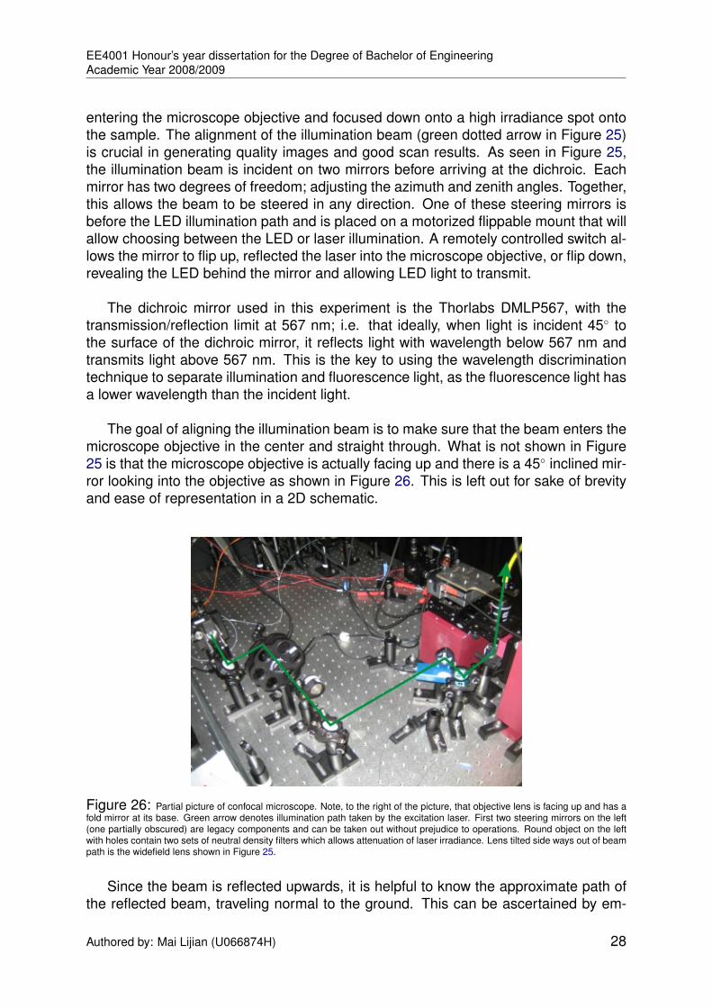
The goal of aligning the illumination beam is to make sure that the beam enters themicroscope objective in the center and straight through. What is not shown in Figure25 is that the microscope objective is actually facing up and there is a 45◦ inclined mir-ror looking into the objective as shown in Figure 26. This is left out for sake of brevityand ease of representation in a 2D schematic.
Figure 26: Partial picture of confocal microscope. Note, to the right of the picture, that objective lens is facing up and has afold mirror at its base. Green arrow denotes illumination path taken by the excitation laser. First two steering mirrors on the left(one partially obscured) are legacy components and can be taken out without prejudice to operations. Round object on the leftwith holes contain two sets of neutral density filters which allows attenuation of laser irradiance. Lens tilted side ways out of beampath is the widefield lens shown in Figure 25.
Since the beam is reflected upwards, it is helpful to know the approximate path ofthe reflected beam, traveling normal to the ground. This can be ascertained by em-
Authored by: Mai Lijian (U066874H) 28

EE4001 Honour’s year dissertation for the Degree of Bachelor of EngineeringAcademic Year 2008/2009
ploying the assistance of a plumbline. As shown in Figures 27(a) and 27.
(a) Using a plumbline totrace out laser path if it weretruly normal to the groundand correctly reflected bythe mirror.
(b) Closeup of Figure 27(a).
Figure 27: Using a plumbline to align microscope.
In Figure 27, the hole which the plumbline cone is enter is where the objective willbe screwed into. The platform which the hole is on has three adjustable knobs whichallows adjustment of the tilt of the objective lens with respect to the ground. It is alsocrucial to make this platform perpendicular to the incoming illumination beam by ad-justing these knobs. A mirror can be placed where the hole is to reflect the incomingillumination beam. If the mirror surface, hence the platform, is perpendicular to theincoming beam the reflected illumination beam will travel back at exactly along thesame path and become coaxial with the incoming illumination beam. The knobs onthe platform should be adjusted until this condition is observed, this will ensure thatwhen the objective lens is screwed into the hole, the incoming illumination beam willbe coaxial with the principal axis of the lens.
As seen in Figure 27(a), a spot is marked on the spot above the microscope objec-tive position, represented by where the plumbline string touches the top structure tobe marked. Every time an alignment is carried out, the illumination beam is moved tohit that spot and the center of the hole where the microscope objective is supposed tosit to ensure the beam will enter the objective lens though the center.
Unfortunately, even with all the aforementioned procedures, it still does not guar-antee that the beam is absolutely entering the objective along the principal axis, but itdoes give a very good rough alignment and a place to start. To ensure that the beamis really coaxial to the principal axis, one must make use of the microscope objective
Authored by: Mai Lijian (U066874H) 29

EE4001 Honour’s year dissertation for the Degree of Bachelor of EngineeringAcademic Year 2008/2009
itself and observe the focused spot on a coverslip under magnification using the CCDcamera. Ideally, an objective lens pointed perpendicularly onto a sample surface asymmetrical Airy disk should be observed. If the lens is tilted relative to the incomingbeam (or vice versa), comatic abberations will be apparent, in the form of the Airydisk having an asymmetrical comet like profile (hence the name comatic abberations)instead of a symmetrically round disk [6]. This would indicate that the beam is enter-ing the objective lens at a slightly tilted angle with respect to the principal axis. Thecomatic abberation can be minimized by carefully adjusting the folding mirror and thecorresponding degree of freedom on the dichroic mirror to compensate for this untila symmetrical Airy disk is formed on screen. This final adjustment to correct for thecomatic abberation will ensure that the beam, microscope objective lens and sampleare all aligned correctly to the principal axis.
In this microscope, the objective lens will play two roles; firstly, to use its large nu-merical aperture to focus light down to a small spot to enhance illumination irradiance,secondly, to use that same numerical aperture to act as a collection optic to enhancethe collection of single photons emitted by the fluorescence of the molecule. Detectionand related issues will be discussed in the next section on detection.
3.1.2 Detection and the Hanbury Brown and Twiss setup
The role of the confocal pinhole in this setup is played by the narrow aperture of asingle mode fibre at the detector, roughly 8µm in diameter. Starting from the top of theschematic, the we see that a 290 ns delay is added one detection arm of the HanburyBrown and Twiss setup. This is due to the 128 ns dead time of the timestamp cardthat forms part of the start-stop measurement device, which makes it unable to mea-sure anything after a detection even has occurred on either the ”start” or ”stop” input.This represents a problem in that g(2)(0) = 0 will always occur due to the dead time,regardless of having anti-bunched photons incident on the detector or otherwise.To compensate for this, a delay has to be added in one arm of the start stop measure-ment. A delay cable of approximately 58 m is added to introduce a delay in one ofthe arms of the start-stop measurement. This effectively shifts the τ=0 point by 290nsand now, both positive and negative time delays can be measured properly. A coax-ial cable from AM Australia is used (MIL-C-17D) with a polyethylene insulator. Fromthe manufacturer’s datasheet, the phase velocity in the cable is vp=2×10⁸m/s and thiscorresponds to the velocity expected with the measured delay time and cable length,i.e,
vp =l
τdelay
(29)
Where τdelay is the delay time between the two detector arms, which is directly dueto the cable, and l is the length of the cable used. Positive time delay, τ >=0, occurswhen a photon activates the start arm before the stop arm and negative time delay,τ <0 occurs when the stop arm actives before the start. The selection and namingof the arms are arbitrary. A actual raw data plot of the g(2)(τ) is shown in Figure 28.This is before the plot is normalized to 1 and zero-shifted to yield a final plot shown in
Authored by: Mai Lijian (U066874H) 30

EE4001 Honour’s year dissertation for the Degree of Bachelor of EngineeringAcademic Year 2008/2009
Figure 47. The resulting g(2)(τ) plot is a histogram of number of photon counts that aretemporally separated by τns.
0 500 1000 1500 2000 2500 30000
200
400
600
800
1000
Time delay ,ô (ns)
Ra
w c
oin
cid
en
ces
Figure 28: A raw plot of the g(2)(τ) function. Note the actual anti-bunching dip at τ=290ns.
Figure 29: Actual picture of the Hanbury Brown and Twiss setup. The two black boxes at the top right hand corner are theAPDs used. The square objective shown on the bottom left corner is the non-polarizing broadband beam-splitter. Just below thebeam-splitter is a highpass filter. The two black objects with three silver handles hold the coupling lens, which is connected to anoptical fibre from the APD.
The photo detectors used in this experiment are Avalanche photodioes (hereafterAPD). The APD is pigtailed to an optical fibre, which is connected to a coupling lens,which collects and focuses light into the optical fibre. The coupling lens in turn, sitson a black mount facing the beam-splitter in the Hanbury Brown and Twiss setip asshown in Figure 29. To adjust the sensory direction of the APDs, there are four de-grees of freedom to be adjusted for the coupling lens. Two to change the cartesianposition of the lens, two to change the azimuth and zenith sensory orientation of the
Authored by: Mai Lijian (U066874H) 31

EE4001 Honour’s year dissertation for the Degree of Bachelor of EngineeringAcademic Year 2008/2009
lens. As both APDs should be taking photon statistics from the same molecule, thus,it is of cardinal import to ensure that both APDs are aligned to observe the same spot.This is done by sending a laser beam out of the coupling lens for both mounts, byconnecting a single mode fibre between the mount and a laser. Lasers of differentcolours are recommended to be able to differentiate which mount needs adjustment.In the setup, a two He-Ne lasers emitting at 590 nm and 632.8 nm are used for thispurpose; as both lasers have different colours and both are able to transmit throughthe high pass filters and dichroic mirror to reach the illumination 532 nm laser for coax-ial alignment. Collimation should be the checked first to ensure all further alignmentsare valid. Collimation checking can be done by intuition from projecting a beam acrossa sufficiently large distance, or by using a shear plate collimation tester. Collimationcan be adjusted by changing the coupling lens distance to the fibre ferrule.
Next, the orientation of the beam-splitter should also be checked to see if it is paral-lel to the ground and have surfaces normal to both input beams. This can be confirmedbut turning the incline and direction of the beam-splitter so that the back reflected laserbeam from each mount can be seen to light up its own optical fibre that is delivering thelaser. Both beams should be combined at the beam-splitter and projected across aneffectively large distance together with the illumination laser; e.g. 10m across the lab.From simple geometry, any number of cylinders can be considered coaxial if they arecoaxial at two points in space. Thus, borrowing from this concept, the detector beamsmust be adjusted using the four degrees of freedom so that their two spots coincidein two spatial coordinates together with the illumination spot, which would have beenalready aligned earlier. Ideally, these two spatial coordinates selected for alignmentshould be as far away as possible from each other. To coincide the beams in the spotnearer to the setup, it would be more convenient to adjust the cartesian degrees offreedom and to reserve the spherical degrees of freedom for the further calibrationspot. This is because spherical arc length changes due to adjusting the azimuth andzenith angles are a function of radial distances; meaning small changes in angles canresult in large changes in distance in the further calibration spot while not changing thespot’s position much in the nearer spot. Thus, by its very nature, the spherical degreesof freedom are more suited for calibrating the further calibration spot.
Often, it takes several iterations between trying to coincide the far and near spotsto achieve coaxial beams. Additionally, the beam heights of the Hanbury Brown andTwiss setup should be coplanar with the illumination laser. Lastly, as different fibreshave different ferrule lengths, it may not be advisable to change fibres connected tothe mounts after the collimation has been set for that particular fibre. Instead, usea mating sleeve to connect other fibres to the calibrated fibre and avoid the need tochange fibres that are already connected to the coupling lens.
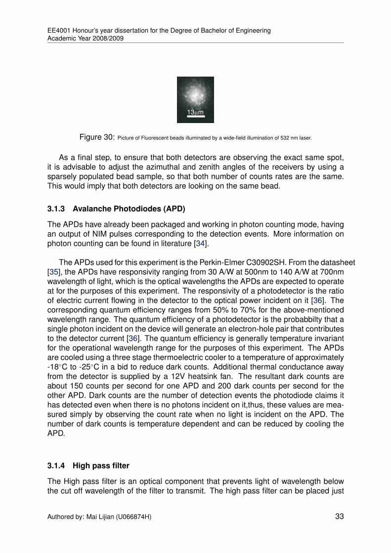
Fluorescent beads are highly useful in aligning the confocal microscope and aas test sample as they approximate point sources, although with diameters of about100nm, technically they are not point sources. They are photostable as they take verylong to bleach, and they are highly fluorescent, suitable for use even in low irradianceconditions. A picture of Fluorescent beads is shown in Figure 30.
Authored by: Mai Lijian (U066874H) 32
EE4001 Honour’s year dissertation for the Degree of Bachelor of EngineeringAcademic Year 2008/2009
13µm
Figure 30: Picture of Fluorescent beads illuminated by a wide-field illumination of 532 nm laser.
As a final step, to ensure that both detectors are observing the exact same spot,it is advisable to adjust the azimuthal and zenith angles of the receivers by using asparsely populated bead sample, so that both number of counts rates are the same.This would imply that both detectors are looking on the same bead.
3.1.3 Avalanche Photodiodes (APD)
The APDs have already been packaged and working in photon counting mode, havingan output of NIM pulses corresponding to the detection events. More information onphoton counting can be found in literature [34].
The APDs used for this experiment is the Perkin-Elmer C30902SH. From the datasheet[35], the APDs have responsivity ranging from 30 A/W at 500nm to 140 A/W at 700nmwavelength of light, which is the optical wavelengths the APDs are expected to operateat for the purposes of this experiment. The responsivity of a photodetector is the ratioof electric current flowing in the detector to the optical power incident on it [36]. Thecorresponding quantum efficiency ranges from 50% to 70% for the above-mentionedwavelength range. The quantum efficiency of a photodetector is the probabbilty that asingle photon incident on the device will generate an electron-hole pair that contributesto the detector current [36]. The quantum efficiency is generally temperature invariantfor the operational wavelength range for the purposes of this experiment. The APDsare cooled using a three stage thermoelectric cooler to a temperature of approximately-18◦C to -25◦C in a bid to reduce dark counts. Additional thermal conductance awayfrom the detector is supplied by a 12V heatsink fan. The resultant dark counts areabout 150 counts per second for one APD and 200 dark counts per second for theother APD. Dark counts are the number of detection events the photodiode claims ithas detected even when there is no photons incident on it,thus, these values are mea-sured simply by observing the count rate when no light is incident on the APD. Thenumber of dark counts is temperature dependent and can be reduced by cooling theAPD.
3.1.4 High pass filter
The High pass filter is an optical component that prevents light of wavelength belowthe cut off wavelength of the filter to transmit. The high pass filter can be placed just
Authored by: Mai Lijian (U066874H) 33

EE4001 Honour’s year dissertation for the Degree of Bachelor of EngineeringAcademic Year 2008/2009
before the beam splitter is used to get rid of any excitation or stray light which willcontaminate the fluoresce signal and cause signal background to increase, thus de-creasing the signal to background or signal to background ratio.
There is also an option to connect one of the arms of the detector to a spectrom-eter, where the incoming light can be decomposed to its various component wave-lengths. The spectrometer also uses the avalanche photodiode(APD) as a photode-tector. Thus, now the APD measures spectral amplitude of the light spectrum. For theinner workings of the spectrometer, see section 3.3.1.
3.1.5 CCD camera and magnification
The camera used is a WATEC WAT 120N-CCIR monochromatic camera with a NikonNikkor zoom objective lens attached (zoom objective lens on the CCD camera shouldnot be confused with the microscope objective lens). In this case, the Nikon zoom ob-jective is acting as the tube lens in the microscope system when the sample is viewedthrough the CCD camera. The zoom objective lens has an adjustable f-number, orf/#, of 4.5 to 5.4 and is used primarily to adjust the zoom and focus of the image.Thef-number is a measure of a lens’ light collection capability and is related to the NA. Thef/# is defined as [6]
f/# =f
D(30)
Where f is the focal length of the lens and D is the diameter of the lens aperture.The focal length of the lens is adjustable from 80mm to 200mm, with 200mm usedto focus objects at infinity. In this case, the fixture of the the zoom objective lens of-fers insufficient distance between the objective lens and the CCD array surface; i.e.the distance between the lens and the CCD array is smaller than the focal length ofthe lens, thus images are all blurred. This is solved by using additional c-mount ringswhich act as extenders, attached between the zoom objective lens and the camera.There is a flippable mirror in front of the CCD camera, this allows us to choose be-tween using the CCD camera as our detection equipment or using the APDs. With theCCD camera, the setup works just like a normal microscope, allow us to see the en-tire sample surface at one go. Whereas using the APD is for confocal scanning, whereone pixel is detected at a time. The APD is much more sensitive than the CCD camera.
Note that using equation 30, calculating for D using the two extreme values yield adifferent answer; i.e. D using f=80 mm and f/# = 4.5 is not equal to D calculated usingf=200 mm and f/# = 5.4. This is because of an additional aperture inside the zoomobjective which has a size smaller than the external lens. This limits the amount oflight going in and changes the effective value of D.
In the current configuration, the focal length of the CCD zoom objective lens is setto be 200 mm to focus to objects at infinity. This will perfectly receive light that exits
Authored by: Mai Lijian (U066874H) 34

EE4001 Honour’s year dissertation for the Degree of Bachelor of EngineeringAcademic Year 2008/2009
the microscope objective lens as the exiting light is also corrected to focus at infinity.Using the equation 10, the current configuration has a magnification of 125X.
3.1.6 Piezo stage and controller
The piezo stage used to move a sample around is shown and this is shown in Figure31.
(a) piezo stage supporting a fork which holds thesample coverslip.
(b) Controller for piezo stage, knobs allow for man-ual control of piezo stage.
Figure 31: Pictures of piezo stage and its controller.
It is from Piezosystem Jena and has a translation range of 80 µm × 80 µm × 80 µmin all three cartesian axes. It is capable of operating in closed loop control mode andthis enables high repeatability in locating a given position. Also, operating in closedloop mode reduces the drift that might occur when operating in open loop mode; leav-ing a piezo stage alone for an hour in open loop mode might cause the piezo stage tolose its intended positioning. However, the translation range is higher when operatingin open loop mode; up to 100 µm × 100 µm × 100 µm. The spatial resolution of thepiezo stage is 1 nm. The piezo stage is controlled by three control voltage channelsfrom the computer that modulates between 0V to 10V, one channel for each axis. Thismodulation voltage is translated linearly into distance translation on the piezo stageby the controller. The controller will in turn, apply a voltage from -10V to 150V on thepiezo stage to drive the stage around. The stage is predominantly used in the positivevoltage regime; from 0V to 150V.
In Figure 32, a grid usually used for transmission electron microscopes is scannedin confocal mode. Each individual square on in Figure 32(a) is 11.5µm across. Theresult is shown in Figure 32(b).
3.1.7 Opto-mechanics
As seen from Figure 33, the confocal microscope had gone through a physical re-design. It was decided to reconfigure the microscope as this allows the use of theoptical table and brings much needed flexibility in altering the topology of various com-ponents of the confocal microscope to suit the nature of the experiment; to have formfollow function. Before the redesign, the setup was mounted on a vertical breadboard
Authored by: Mai Lijian (U066874H) 35

EE4001 Honour’s year dissertation for the Degree of Bachelor of EngineeringAcademic Year 2008/2009
(a) Picture of grids being scanned as viewed fromthe CCD camera. Each square is 11.5µm across
(b) Confocal scan of calibration grids.
Figure 32: Comparison of CCD image and confocal scan.
as shown in Figure 33(a) when it was first inherited. After the re-design, it is as shownin Figure 33(b). The red blocks which were missing in the old setup is shown in Figure34.
These blocks are created by using a computerized numerical control (hereafterCNC) machine. The programming of these machines is in a language known as G-code. The design drawings of these components are shown in the appendices.
Another advantage of this new setup is that now, the microscope objective lens isfacing upwards instead of downwards. This reduces the danger of crashing the mi-croscope objective lens into the sample when the objective lens is over driven; thiscan happen when the user is trying to obtain a focus, but has already gone beyondthe plane of focus without knowing it. As in the old configuration, the entire weight ofthe objective lens will bear onto the coverslip, causing it to break as it is compressedbetween the old holder and the objective lens. The shattering glass may scratch theobjective lens, rendering it unusable. In the new configuration, the microscope ob-jective lens will merely push the coverslip and cause it to balance on the microscopeobjective lens instead. Also, changing of samples is easier with the new objective lensnow that the user does not have to drive the objective up just to change a sample asthe sample is easily accessible from the top, not compressed between the microscopeobjective and the stage below.
Authored by: Mai Lijian (U066874H) 36

EE4001 Honour’s year dissertation for the Degree of Bachelor of EngineeringAcademic Year 2008/2009
(a) Inherited setup. (b) Setup status quo.
Figure 33: Setup now and then.
Figure 34: Red blocks and silver fork on top are new additions to the microscope design.
3.2 Light emitting diodes (LEDs)
As LEDs are extensively used in the experiment, a summary of work done on LEDs isgiven here. Noting the physical features, spectral and optical characteristics.
3.2.1 LED physical structure
The various subfigures of Figure 35 shows different views of a typical high power LED,in this case, selected to be the Luxeon K2 for illustration purposes notwithstandingnot being used heavily in the experiment. The Luxeon Rebel, which is used in theexperiment, does not have physical characteristics such as bonding wires or a largelens as in in Figure 35(b) and 35(c) respectively. In Figure 35(b), the red object in themiddle is the LED die (sometimes referred to as the LED chip) and is the light emittingobject of the LED. The two golden objects rising out of the sides are bonding wires and
Authored by: Mai Lijian (U066874H) 37
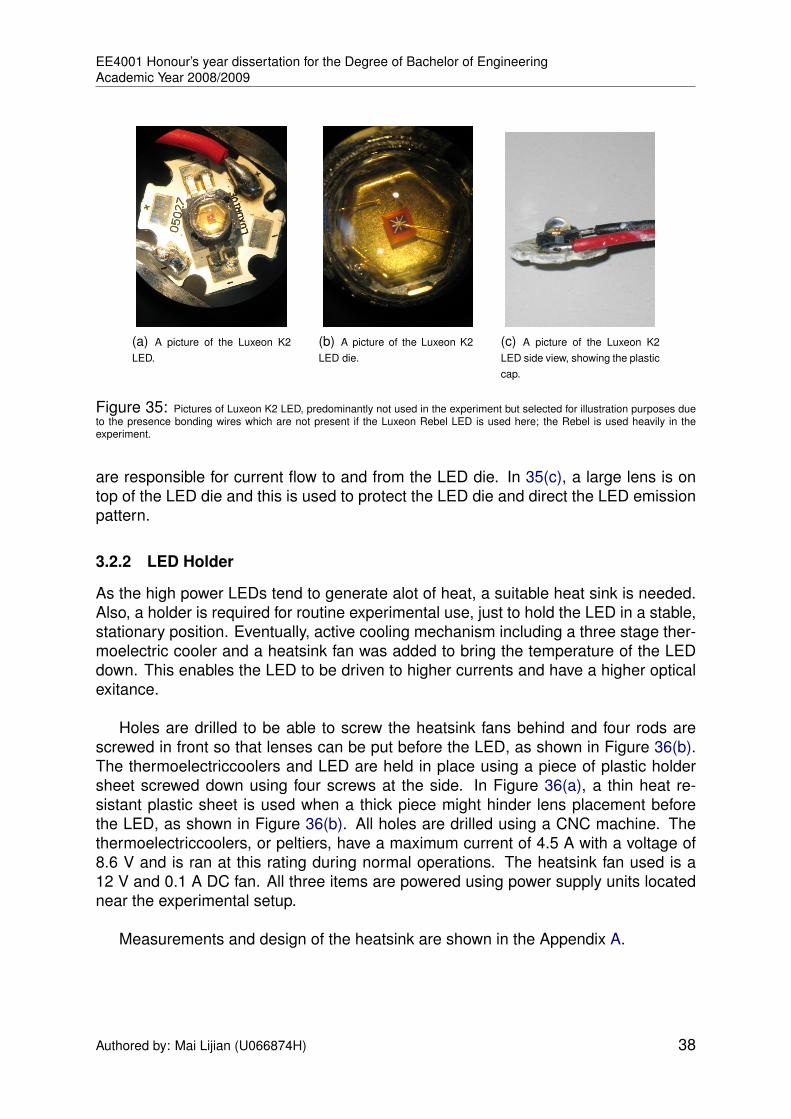
EE4001 Honour’s year dissertation for the Degree of Bachelor of EngineeringAcademic Year 2008/2009
(a) A picture of the Luxeon K2LED.
(b) A picture of the Luxeon K2LED die.
(c) A picture of the Luxeon K2LED side view, showing the plasticcap.
Figure 35: Pictures of Luxeon K2 LED, predominantly not used in the experiment but selected for illustration purposes dueto the presence bonding wires which are not present if the Luxeon Rebel LED is used here; the Rebel is used heavily in theexperiment.
are responsible for current flow to and from the LED die. In 35(c), a large lens is ontop of the LED die and this is used to protect the LED die and direct the LED emissionpattern.
3.2.2 LED Holder
As the high power LEDs tend to generate alot of heat, a suitable heat sink is needed.Also, a holder is required for routine experimental use, just to hold the LED in a stable,stationary position. Eventually, active cooling mechanism including a three stage ther-moelectric cooler and a heatsink fan was added to bring the temperature of the LEDdown. This enables the LED to be driven to higher currents and have a higher opticalexitance.
Holes are drilled to be able to screw the heatsink fans behind and four rods arescrewed in front so that lenses can be put before the LED, as shown in Figure 36(b).The thermoelectriccoolers and LED are held in place using a piece of plastic holdersheet screwed down using four screws at the side. In Figure 36(a), a thin heat re-sistant plastic sheet is used when a thick piece might hinder lens placement beforethe LED, as shown in Figure 36(b). All holes are drilled using a CNC machine. Thethermoelectriccoolers, or peltiers, have a maximum current of 4.5 A with a voltage of8.6 V and is ran at this rating during normal operations. The heatsink fan used is a12 V and 0.1 A DC fan. All three items are powered using power supply units locatednear the experimental setup.
Measurements and design of the heatsink are shown in the Appendix A.
Authored by: Mai Lijian (U066874H) 38
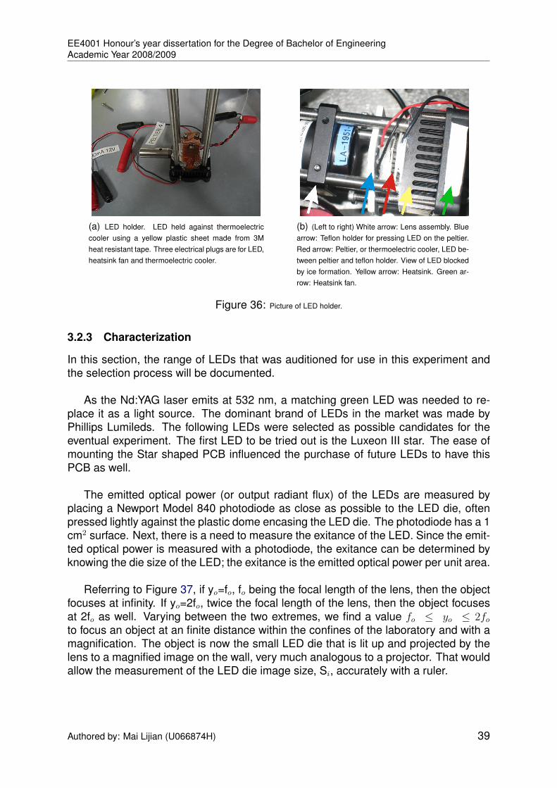
EE4001 Honour’s year dissertation for the Degree of Bachelor of EngineeringAcademic Year 2008/2009
(a) LED holder. LED held against thermoelectriccooler using a yellow plastic sheet made from 3Mheat resistant tape. Three electrical plugs are for LED,heatsink fan and thermoelectric cooler.
(b) (Left to right) White arrow: Lens assembly. Bluearrow: Teflon holder for pressing LED on the peltier.Red arrow: Peltier, or thermoelectric cooler, LED be-tween peltier and teflon holder. View of LED blockedby ice formation. Yellow arrow: Heatsink. Green ar-row: Heatsink fan.
Figure 36: Picture of LED holder.
3.2.3 Characterization
In this section, the range of LEDs that was auditioned for use in this experiment andthe selection process will be documented.
As the Nd:YAG laser emits at 532 nm, a matching green LED was needed to re-place it as a light source. The dominant brand of LEDs in the market was made byPhillips Lumileds. The following LEDs were selected as possible candidates for theeventual experiment. The first LED to be tried out is the Luxeon III star. The ease ofmounting the Star shaped PCB influenced the purchase of future LEDs to have thisPCB as well.
The emitted optical power (or output radiant flux) of the LEDs are measured byplacing a Newport Model 840 photodiode as close as possible to the LED die, oftenpressed lightly against the plastic dome encasing the LED die. The photodiode has a 1cm2 surface. Next, there is a need to measure the exitance of the LED. Since the emit-ted optical power is measured with a photodiode, the exitance can be determined byknowing the die size of the LED; the exitance is the emitted optical power per unit area.
Referring to Figure 37, if yo=fo, fo being the focal length of the lens, then the objectfocuses at infinity. If yo=2fo, twice the focal length of the lens, then the object focusesat 2fo as well. Varying between the two extremes, we find a value fo ≤ yo ≤ 2foto focus an object at an finite distance within the confines of the laboratory and with amagnification. The object is now the small LED die that is lit up and projected by thelens to a magnified image on the wall, very much analogous to a projector. That wouldallow the measurement of the LED die image size, Si, accurately with a ruler.
Authored by: Mai Lijian (U066874H) 39

EE4001 Honour’s year dissertation for the Degree of Bachelor of EngineeringAcademic Year 2008/2009
SoSi
yoyi
Figure 37: Imaging and magnifying LED die on a screen far away. So being the object size, Si being the image size, yo
being the object distance from the lens and yo being the image distance from the lens
Noting that transverse magnification [6],
MT =yiyo
=SiSo
(31)
With measured Si, yo and yi, So can be easily calculated using equation 31.
LED Maximum Voltage (V) Radiant Die Exitancecurrent (mA) flux (mW) area (mm2) (KW/m2)
Luxeon III 1000 3.6 113 2.465 46Luxeon K2 1500 4.1 147 2.465 59
Luxeon Rebel 700 3.3 198 2.465 80
Table 1: Table of different green LEDs tested. Maximum current is taken from datasheet.
The specific model numbers for the LEDs are, for the Luxeon III, LXHL-LM3C. TheLuxeon K2, LXK2-PM14-U00 and for the Luxeon Rebel, LXML-PM01-0080. From Ta-ble 1, it is clear that the Rebel is the LED of choice. Moreover, looking at Figure 38,it is possible to see that the Rebel has a narrower spectrum. Thus, more of the ra-diant flux will be focused in the relevant spectral range in the Rebel compared to thethe other LEDs. Using an ad-hoc yardstick to compare exitance per FWHM spectrallinewidth nm, we see that the Luxeon Rebel has a most of the light concentrated withinthe spectral region around the dominant wavelength; this name is shown in Table 2.This will be important when a filter is used in front of the LED to filter off unwanted lighttoo far beyond the dominant wavelength. Thus, having optical power in those spectralareas may even complicate the filtering process (see Section 4.2.1 for more on spec-tral filtering).
In the course of looking at the different LEDs, it is discovered that there are twovarieties of Luxeon Rebel LEDs, both having the model number LXML-PM01-0080.The LED with the white die often has more optical power output compared to the LEDwith the black die.
By using appropriate cooling methods described in section 3.2.2, the LED will bedriven over the rated limit of 700mA. The LED radiant flux vs input current curve isplotted in Figure 40. As these values are taken when the LED is cooled, the values
Authored by: Mai Lijian (U066874H) 40
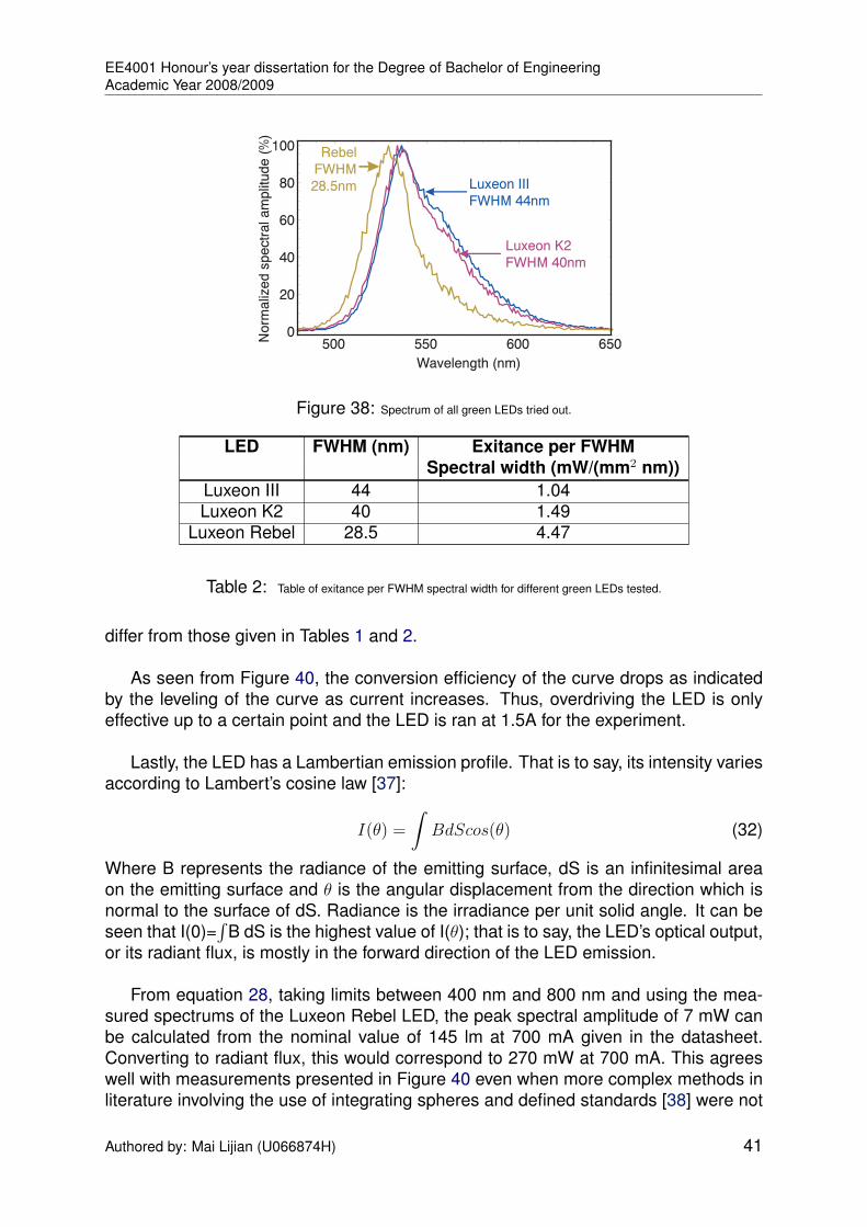
EE4001 Honour’s year dissertation for the Degree of Bachelor of EngineeringAcademic Year 2008/2009
500 550 600 6500
20
40
60
80
100
Wavelength (nm)
RebelFWHM
28.5nm
Luxeon K2FWHM 40nm
Luxeon III FWHM 44nm
No
rma
lize
d s
pe
ctr
al a
mp
litu
de
(%
)
Figure 38: Spectrum of all green LEDs tried out.
LED FWHM (nm) Exitance per FWHMSpectral width (mW/(mm2 nm))
Luxeon III 44 1.04Luxeon K2 40 1.49
Luxeon Rebel 28.5 4.47
Table 2: Table of exitance per FWHM spectral width for different green LEDs tested.
differ from those given in Tables 1 and 2.
As seen from Figure 40, the conversion efficiency of the curve drops as indicatedby the leveling of the curve as current increases. Thus, overdriving the LED is onlyeffective up to a certain point and the LED is ran at 1.5A for the experiment.
Lastly, the LED has a Lambertian emission profile. That is to say, its intensity variesaccording to Lambert’s cosine law [37]:
I(θ) =
∫BdScos(θ) (32)
Where B represents the radiance of the emitting surface, dS is an infinitesimal areaon the emitting surface and θ is the angular displacement from the direction which isnormal to the surface of dS. Radiance is the irradiance per unit solid angle. It can beseen that I(0)=
∫B dS is the highest value of I(θ); that is to say, the LED’s optical output,
or its radiant flux, is mostly in the forward direction of the LED emission.
From equation 28, taking limits between 400 nm and 800 nm and using the mea-sured spectrums of the Luxeon Rebel LED, the peak spectral amplitude of 7 mW canbe calculated from the nominal value of 145 lm at 700 mA given in the datasheet.Converting to radiant flux, this would correspond to 270 mW at 700 mA. This agreeswell with measurements presented in Figure 40 even when more complex methods inliterature involving the use of integrating spheres and defined standards [38] were not
Authored by: Mai Lijian (U066874H) 41

EE4001 Honour’s year dissertation for the Degree of Bachelor of EngineeringAcademic Year 2008/2009
(a) A picture of the Luxeon Rebel LED with a shinyblack die.
(b) A picture of the Luxeon Rebel LEDwith a white die.
Figure 39: Rebel die types.
0.2 0.4 0.6 0.8 1 1.2 1.450
100
150
200
250
300
Current (A)
Ra
dia
nt
flu
x /
O
utp
ut
op
tica
l po
we
r (m
W)
Figure 40: Green Rebel LED radiant flux vs input current.
used.
3.3 Spectrometer
3.3.1 Principles of operation
Shown in Figure 41 is a schematic of a spectrometer. At the heart of this spectrometeris a reflection grating. It is basically a piece of substrate with very fine trenches carvedout on the surface of the substrate. The grating used in this experiment has a trenchwidth of just 833nm or 1200 trenches per millimeter, denoted as ”a” in Figure 41. Notethat for the purposes of illustration, the trench is defined here as containing part ofthe top plateau as well. As shown in Figure 41, when a beam of light is incidenton the surface of the grating, several orders of reflection is observed off the grating.The zeroth order being the reflection order that obeys the law of reflection where theangle of reflection is equivalent to the angle of incidence. The orders of reflection aregoverned by the grating equation reproduced below [6],
mλ
a= sinθm − sinθi (33)
Authored by: Mai Lijian (U066874H) 42

EE4001 Honour’s year dissertation for the Degree of Bachelor of EngineeringAcademic Year 2008/2009
From source
To APD
Rotatable reflectiongrating, a=833.3nm
a
n=0
n=-1
n=-2
n=1
n=2
èi
èm
Figure 41: Schematic of a spectrometer, reflection grating is placed on a stepper motor and controlled by a motor driver. ndenotes the nth order reflection, with the zeroth order reflection is the same as the incidence angle, i.e. θ0 = θi.
Where m is the order of reflection, a is the grating spacing between two adjacent grat-ing peaks as illustrated in Figure 41, θi is the incidence angle and θm is the angle ofreflection for the mth order. These notations are illustrated in Figure 41. Thus, the an-gle of reflection for higher order reflections is a function of wavelength, thus a beam oflight of multiple wavelengths will be broken up into a radial spectrum by the grating. Asthe grating turns, only one wavelength should be reflected into the detection path bythe mirror. This would be especially true if a single mode fibre is placed at the end ofthe detection path; as it will only allow one mode and one wavelength to be measuredat any one time. Therefore, using a single mode fibre will usually give a higher spectralresolution.
The spectrometer topology used in this experiment is specifically designed so thatwhen θi=0, the 1st order reflection of a 632.8 nm He-Ne laser is exactly being de-tected by the spectrometer. Having a such a laser at hand makes the alignment of thespectrometer easy as the 632.8 nm laser is able to act as a control measurement foralignment. The angular displacement between the source beam and the mirror canbe calculated easily using this scenario and equation 33 by setting λ=632.8 nm, θi=0,m=1, a=833 nm. This means that the angular displacement between the source beamand the mirror is 49.434◦ or 0.8627 rad. This value is fixed as the components of thespectrometer and is a constant throughout the spectrometer operation.
To APDn=1 ë1
ë2
èi
è1
Figure 42: First order reflection is a function of wavelength. Colour is indicative of relative wavelength; λ1 > λ2.
Here, an equation to relate grating angle and the wavelength being observed bythe detection arm will be derived. Since the spectrometer is supposed to work in onlythe first order reflection mode, therefore, m=1. As illustrated in Figure 42, the grating
Authored by: Mai Lijian (U066874H) 43

EE4001 Honour’s year dissertation for the Degree of Bachelor of EngineeringAcademic Year 2008/2009
angle , driven by the stepper motor, is equal to the incidence angle θi and will be usedinterchangeably hereafter. Therefore equation 33 will now be
λ
833nm= sinθ1 − sinθi (34)
As above-mentioned,θi + θ1 = 49.434◦ (35)
Substituting 35 into 34
∴ sin(49.434◦ − θi)− sin(θi) =λ
833nm(36)
Using identity,sin(α± β) = sin(α)cos(β)± cos(α)sin(β) (37)
0.7584cos(θmot)− 1.651sin(θmot) = 1.2× 10⁶λ (38)
Using identity,αcos(θ)± βsin(θ) =
√α2 + β2cos(θ ∓ γ) (39)
Where γ = tan−1(βα
)We arrive at the equation to express wavelength being observed by detector in termsof motor angle,
λ = 1.514× 10⁶cos(θi + 1.1404)m (40)
Or conversely,θi = cos−1(660.22× 10³λ)− 1.14rad (41)
Note that angle of grating, θi < 49.434◦ to prevent the zeroth order reflection from beingobserved by the detector, thereby operating beyond the first order regime. This equa-tion is currently programmed within the motor controller and rounds off automatically.
However, for convenience sake, one can also take a linear approximation. By plot-ting the graph for, dθ
dλ, we can approximate the number of motor steps to move in order
to change the observed spectral wavelength. This will be shown below. Noting that[39],
d cos-1(θ)
dλ= − 1√
1− θ2(42)
∴dθidλ
= − 6558857.44√1− 4.30186× 10¹¹λ2
rad/m (43)
Converting the rad/m expression to number of motorized steps per nm is trivial, as thestepper motor used has, mathematically, 3642.88 steps per degree.Thus,
dθidλ
= −(10−9)(3642.88)(180
π)
6558857.44√1− 4.30186× 10¹¹λ2
steps/nm (44)
By plotting equation (44), shown in Figure 43, we see that the number of stepsper nm is roughly 150 for the operational wavelength we usually work at (400nm to800nm). That is to say, moving by 150 steps will change from observing 600nm to
Authored by: Mai Lijian (U066874H) 44

EE4001 Honour’s year dissertation for the Degree of Bachelor of EngineeringAcademic Year 2008/2009
601nm or 599nm, depending on the direction turned. This is especially useful in align-ing the spectrometer. Usually, the spectrometer might only be a few nm off but hasthe correct profile. All that would be needed is to reset the zero point where the spec-trometer is calibrated at. This approximation makes it easy to find the number of stepsneeded to move from looking at how many nanometers the spectrum is off the desiredtarget; during alignment, the desired target is the He-Ne 632.8nm. The zero can bereset after moving the grating to compensate for the offset inaccuracies.
200 400 600 800 1000
140
150
160
170
180
Wavelength (nm)
dèi
dë
100
Figure 43: Number of steps to turn to move observation by 1nm.
To align the spectrometer, firstly check that the first order reflections on both sidesof the grating are of the same height over a long distance, this will ensure that gratingis parallel to the ground. As the He-Ne laser is likely to hit the laser when the grating isat its default position with its surface normal to the incoming beam, a lower wavelengthlaser beam can be used instead to facilitate the projection of the reflection over a largerdistance. Secondly, the mirror is mounted in such a way that there are two degreesof freedom to be adjusted; its azimuth and zenith angles. Adjust these angles suchthat the reflected beam is in the same plane as the two first order reflected beamsearlier. Lastly, adjust the focusing lens which will couple the light into the optical fibreconnected to the APD. This lens is extremely sensitive to movement and its correctposition is crucial to the alignment of the system, thus, positioning of this lens on amicrometer positioning system is advised. By reading off the APD, minor adjustmentsto all three angles can be made to maximize the APD reading, thereby ensuring thehighest coupling efficiency into the APD.
3.3.2 Characterization
The throughput of the spectrometer is measured by plugging in 700µW of He-Ne laserlight and measuring approximately 200µW of output optical power. This implies thatthe throughput of the spectrometer is 28%; that is, 28% of the light is in one of the firstorder reflections off the grating. This is to be expected the measured power is only oneof the two first order reflections. Optical power is lost to the other first order reflection,
Authored by: Mai Lijian (U066874H) 45

EE4001 Honour’s year dissertation for the Degree of Bachelor of EngineeringAcademic Year 2008/2009
632.0 632.5 633.0 633.5
2000
4000
6000
8000
Wavelength (nm)
AP
D c
oun
ts p
er
seco
nd
FWHM≈0.4nm±0.05nm
Figure 44: Results of a test measuring a He-Ne 632.8nm laser spectrum 10 consecutive times.Amplitude fluctuation can be explained by irradi-ance fluctuation of the He-Ne laser used, whichcan even be see by the unaided eye. Spectralprofile consistency and accuracy are satisfactory.Arrow indicates full width half maximum (hereafterFWHM), which is about 0.4 nm.
Figure 45: Actual picture of the spectrometer. Blue box:Lens with focal length, f=100mm in a tube holder with microme-ter screw to adjust distance from fibre. Purple box: Mirror withspherical coordinate adjusting screws. Green box: stepper mo-tor controlling grating postiion. Red box: Reflection grating onmount.
the zeroth order reflection back into the laser and other coupling inefficiencies. Also,referring to Figure 44, the full width half maximum (FWHM) of the He-Ne is measuredto be 0.4 nm. Lasers have a much narrower line width compared to this, thus it isevident that this measurement is limited by the grating resolution, i.e. the resolutionlimit of the spectrometer is 0.4 nm.
3.4 Sample preparation
In this chapter, methods to cleaning coverslips and preparing samples will be intro-duced. This is the process whereby the molecules to be observed and the host matrixthat holds the molecules in place are deposited onto the coverslip. Processes arecarried out on a wet solvent bench. As this processes involve dangerous chemicals,safety wear should be donned at all times; lab coat, gloves and safety goggles. Safedisposal of these chemicals is also carried out by employing a waste disposal servicerather than pouring the used chemical into the sink.
3.4.1 Coverslip cleaning
When attempting to image extremely small particles such as single molecules, it iscrucial to ensure that the surroundings which the molecules reside are free from un-wanted particles such as dirt or water droplets; as very sensitive detection will be usedto detect very weak signals from the molecules, any brightly fluorescing dirt will easilybe detected and mistaken as a fluorescent single molecule. Although having a clean
Authored by: Mai Lijian (U066874H) 46
EE4001 Honour’s year dissertation for the Degree of Bachelor of EngineeringAcademic Year 2008/2009
working environment is important, ensuring that the coverslips are clean during thepreparation process is absolutely crucial to the potential usefulness of the sample. Asthe sample is coated onto the coverslip, any residual impurities present on the cover-slip during the preparation process will be permanently embedded onto the sample.
To clean the coverslips, a chain of solvents is used to progressively wash away sur-face contaminants. At every one stage of the solvent chain, the coverslips are placedin a clean glass beaker filled with the particular solvent and everything is placed ina ultrasonic bath of 25 Hz to 45 Hz for 15 minutes. The successive solvents usedare acetone, isopropyl alcohol and methanol in the said order. Acetone is used to re-move organic compounds such as dust or dirt and isopropyl alcohol is used to removenon-polar compounds such as grease and oil. Lastly, methanol is used to removethe isopropyl alcohol. Methanol is highly volatile and evaporates quickly on its own.Ethanol can also be used to replace methanol.
After the solvent chain is completed, all coverslips are placed in a beaker of Piranhasolution until it is required to be used. The Piranha solution consists of a ratio of twoparts of concentrated 98% sulphuric acid (H2SO4) and one part concentrated 40%hydrogen peroxide (H2O2). The Piranha solution derives its name from its ability ofaggressively attack and dissolve organic molecules is also plays the role as a final or-ganic contaminant removal solvent. When required to be used, a coverslip is removedfrom the Piranha solution using a stainless steel tweezer. The coverslip is then rinsedwith distilled water to wash away the Piranha solution. The distilled water is then re-moved from the coverslip using a nitrogen air gun to blow the water off the coverslipsurface. Finally, the samples are spin coated onto the coverslip.
There are other methods available in literature to clean coverslips, but this methodis employed for its simplicity and availability of chemicals in the lab.
3.4.2 Host matrix
Two host matrices are used in the experiment, predominantly p-terphenyl, althoughPMMA/MA was also used in the initial phases of the experiment. Both host matricesare originally in the form of a white powder. Their solutions are prepared in the sameway but different concentrations were used. For PMMA/MA, the resulting concentrationwas 20 mg/mL in toluene and for p-terphenyl it was 3 mg/mL in toluene. An ultrasonicbath for 30 min can also be performed to ensure homogeneity.
3.4.3 Fluorescent molecules
Terrylene comes in the form of shiny black powder in its pure form. To be able todeposit single molecules on the surface, it must be diluted down to an extremely lowconcentration. This is done by dissolving the terrylene powder into a toluene solvent.Generally, toluene dissolves most organic substances easily. A grain of terrylene pow-der of approximately 100 µm diameter is taken and placed into a small vial of tolueneof roughly 10 mL. After which, the mixture is placed in an ultrasonic bath for about 30
Authored by: Mai Lijian (U066874H) 47

EE4001 Honour’s year dissertation for the Degree of Bachelor of EngineeringAcademic Year 2008/2009
Figure 46: A picture of a spin coating machine, the coverslip is placed on the middle silver disk. Hole in the middle isconnected to a vacuum pump and coverslip is held in place by vacuum during the spinning, in which the silver disk and the whitecollar disk spins at high velocity.
mins. The resulting solution should be evenly pink in colour and still transparent. Overtime, the toluene may evaporate in storage, leaving the molecules behind in the vial,simply pour toluene back into the vial and perform an 30 min ultrasonic bath to restorethe molecules into a solution.
3.4.4 Fluorescent beads
The fluorescent beads is originally a thick, bright pink coloured liquid. The beads arediluted using water in the ratio of 1 part bead solution to 10 parts water and spin coatedon a coverslip. The resulting sample and concentration is shown in Figure 30.
3.4.5 Spin coating
In spin coating, a sample that needs to be deposited is placed on the coverslip byusing a pipette. After which, the spincoating machine is programmed with the desiredspin frequency and duration of spinning. Following from similar experiments found inliterature [24], a spinning frequency of 1000 revolutions per minute (hereafter RPM) for30 s followed by 3000 RPM for 2 s. The resulting thickness of the film is 20 nm [24].To spin coat Fluorescent beads, the diluted sample can simply be placed on the cover-slip. To spincoat the molecules however, the diluted terrylene solution has to be mixedwith the host matrix solution first before spin coating. Firstly, extract a portion of thehost matrix solution for use. The required concentration is so sparse that a needleis used by dipping the needle into the terrylene solution, taking it out of the terrylenesolution and dipping it in a sample of the host matrix solution. The minute amountneeded is the amount that is held by the surface tension between the needle surfaceand the terrylene solution.
Authored by: Mai Lijian (U066874H) 48
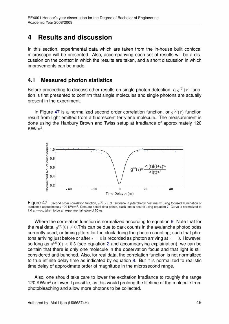
EE4001 Honour’s year dissertation for the Degree of Bachelor of EngineeringAcademic Year 2008/2009
4 Results and discussion
In this section, experimental data which are taken from the in-house built confocalmicroscope will be presented. Also, accompanying each set of results will be a dis-cussion on the context in which the results are taken, and a short discussion in whichimprovements can be made.
4.1 Measured photon statistics
Before proceeding to discuss other results on single photon detection, a g(2)(τ) func-tion is first presented to confirm that single molecules and single photons are actuallypresent in the experiment.
In Figure 47 is a normalized second order correlation function, or g(2)(τ) functionresult from light emitted from a fluorescent terrylene molecule. The measurement isdone using the Hanbury Brown and Twiss setup at irradiance of approximately 120KW/m2.
- 40 - 20 0 20 400.2
0.4
0.6
0.8
1.0
(2)g (ô)=<I(t)I(t+ô)>
2<I(t)>
No
rma
lize
d N
o.
of
co
inci
de
nce
s
Time Delay ,ô (ns)
Figure 47: Second order correlation function, g(2)(τ), of Terrylene in p-terphenyl host matrix using focused illumination ofirradiance approximately 120 KW/m2. Dots are actual data points, black line is best fit using equation 7. Curve is normalized to1.0 at τ=∞, taken to be an experimental value of 50 ns.
Where the correlation function is normalized according to equation 9. Note that forthe real data, g(2)(0) 6= 0.This can be due to dark counts in the avalanche photodiodescurrently used, or timing jitters for the clock doing the photon counting; such that pho-tons arriving just before or after τ = 0 is recorded as photon arriving at τ = 0. However,so long as g(2)(0) < 0.5 (see equation 2 and accompanying explaination), we can becertain that there is only one molecule in the observation focus and that light is stillconsidered anti-bunched. Also, for real data, the correlation function is not normalizedto true infinite delay time as indicated by equation 8. But it is normalized to realistictime delay of approximate order of magnitude in the microsecond range.
Also, one should take care to lower the excitation irradiance to roughly the range120 KW/m2 or lower if possible, as this would prolong the lifetime of the molecule fromphotobleaching and allow more photons to be collected.
Authored by: Mai Lijian (U066874H) 49

EE4001 Honour’s year dissertation for the Degree of Bachelor of EngineeringAcademic Year 2008/2009
4.2 Experiments with LED illumination
4.2.1 Spectral filtering
As the exitance spectrum from an LED is broadband, there is some difficulty in tryingto filter the excitation light from the emission light. This represents a problem as theexcitation light can actually be reflected off the glass coverslip due to Rayleigh scatter-ing in addition to unwanted background fluorescence [16, 13]. These undesirable lightthen propagate back into the detection path. Thus, there are three components in thelight emitted by the sample; the back reflected illumination light, the legitimate molec-ular fluorescence and the background fluorescence. Removing the illumination lightcomponent is not a problem for lasers, for lasers only has a very narrow spectral band-width and easily filtered off by the dichroic mirror or a High pass filter.But for LEDs,the broadband emission means that the back reflected light is also broadband andcan be transmitted through the dichroic mirror and high pass filters. As backgroundfluorescence induces a red-shift in the scattered light with respect to the incident light,eventually some of this scattered light might be transmitted through the dichroic mirrorand reach the detectors. This reduces the signal to background ratio as the scatteredlight becomes indistinguishable from real fluorescence. Usage of quartz coverslip isalso recommended in for lesser fluorescence [13], but is not available for this experi-ment. This is concept is illustrated in Figure 48.
400 500 600 700 800
0
20
40
60
80
100 High passfilter
Wavelength (nm)
No
rma
lize
d s
pe
ctra
l am
plit
ud
e (
%)
Luxeon RebelGreen LED
Nd:YAG laser
Terrylene emission
Wavelength Discrimination Filtering
Excitation light throughfilter
Excitation light throughfilter and overlapping with molecular emission
Figure 48: Cutting off excitation light from being detected is easier with the laser than with the LED. This is especially truefor the red shaded region; it can be indistinguishable from legitimate fluorescence and contributes to background signal. Also,cutting off this light will compromise legitimate molecular emissions.
Of the many filters available in the lab, there needs to be a way to find the opti-mum filter to use in conjunction to the light emitted from the molecules and the lightfrom the LED. To facilitate in the selection of the optimum filter function, the transmis-sion spectra of all filters are scanned using a Perkin-Elmer Lambda 950 spectrometer.Subsequently, to calculate the most efficient illumination filter for the LED, a numericalcalculation is performed with the software Mathematica in which the expression:
Authored by: Mai Lijian (U066874H) 50

EE4001 Honour’s year dissertation for the Degree of Bachelor of EngineeringAcademic Year 2008/2009
∫l(λ)[
∏f(λ)]a(λ)dλ (45)
yields the largest numerical value for different sets of filter transmission spectrum,∏f(λ). Where l(λ) describes the excitation source emission spectrum and a(λ) de-
scribes the absorption spectrum of the molecules. l(λ) can either be the LED or thelaser spectrum. The largest value will then correspond to the best spectral efficiencywhen exciting the molecules. After comparing the various filters, the following oneyields the best overlap with the LED and the molecular absorbtion, the Photonik band-pass filter, shown as ”BP500580” in Figure 49. The absorption spectrum is measuredby putting a concentrated sample of molecules suspended in liquid solvents held byquartz cuvettes into the Perkin-Elmer Lambda 950 transmission spectrometer. Theemission spectrum is then the mirror image but offset by the Stokes shift, as shown inFigure 2.
A corresponding calculation is also performed with the emission and detection armof the confocal microscope. This is shown in Figure 50 by evaluating equation 46∫
e(λ)[∏
f(λ)]dλ (46)
Where e(λ) is the molecular emission spectrum.
400 500 6000
20
40
60
80
100
Wavelength (nm)No
rma
lized S
pect
ral a
mplit
ude (
%)
LED
BP500580Bandpass
filter
Terryleneabsorption
Spectral overlap
Figure 49: Exciter filter with the best spec-tral overlap with absorption spectrum of Terrylene.Here we assume that the reflection bandwidth ofthe dichroic is infinitely broad. Evaluating equation45 will yield a 30% of LED power being incident onmolecules.
LED
400 500 600 7000
20
40
60
80
Wavelength(nm)
ThorlabsDichroic
XR3002
TerryleneEmission
Norm
aliz
ed s
pect
ral a
mplit
ude (
%)
Spectral overlap
100
Figure 50: Detector high-pass filter with the best spectraloverlap with emission spectrum of Terrylene. The orange portiondenotes the signal from the molecular fluorescence and the redregion denotes the background contributed by the LED. Evalu-ating equation 45 will yield a 70% fluorescent light reaching thedetectors.
However, although they produce the most efficient transmission of the LED lightand the best detection of fluorescence light individually, their combined usage is notfavorable as a relatively large portion (3%) of the filtered LED light leaks through thedichroic mirror and high pass filter to reach the detectors; which can be easily detected
Authored by: Mai Lijian (U066874H) 51

EE4001 Honour’s year dissertation for the Degree of Bachelor of EngineeringAcademic Year 2008/2009
in sensitive detection. This is shown in Figure 51.
400 500 600 700 8000
20
40
60
80
100
Wavelength (nm)No
rma
lize
d s
pe
ctra
l am
plit
ud
e (
%)
LED + BP500580 Terrylene +
dichroic +high pass filter
LED light leakage
Figure 51: Individually optimal filters for detection and emission arms of the confocal microscope may not yield the bestresult.Red portion denotes protion of light that still enters detectors. Blue line is the spectrum of filtered light using the PhotonikBP500580 and purple line is the combined transmission spectrum of the Thorlabs dichroic AND the XR3002 high pass filter. Thered shaded region denotes 3% of the LED light leaking through the high pass filter and dichroic mirror.
Note that Figure 51, the peak amplitudes of the plots are normalized to 100% aspotraying the profiles is the main aim of the figure. As seen in Figure 51, any attemptsto shift the high pass filter to the a higher cut off wavelength will further attenuatelegitimate signals from the fluorescent molecules. Moving the bandpass filter to alower wavelength band will also cut off the frequency components that overlap withthe terrylene dominant absorption wavelength. Thus, both situations are unfavorable.In section 4.2.5, the ideal filter cutoff frequency for both filters will be calculated.
4.2.2 Spectral coverage of LED
Apart from its low cost and compactness, the broadband emission of an LED alsomeans that the spectral overlap of the LED is superior to that of a laser’s narrowbandspectrum. If we set: ∫
lLED(λ)[∏
f(λ)]dλ =
∫llaser(λ)[
∏f(λ)]dλ (47)
where lLED(λ) is the emission spectrum of the LED, llaser(λ) is the emissions spec-trum of the laser and
∏f(λ) is the product of all filter transfer functions, including that
of the dichroic mirror. Thus,∫lLED(λ)[
∏f(λ)]dλ is the irradiance on the molecules due
to LED excitation,∫llaser(λ)[
∏f(λ)]dλ is the irradiance on the molecules due to laser
excitation. Using Mathematica to perform numerical analysis, we are able to have a38% in power available to the molecule. This concept is illustrated below in Figure 52.Note however, for sake of clarity, conditions describe by equation 47 is not representedin Figure 52; i.e. the laser and LED powers are not the same in this case, but bothspectral amplitudes are normalized to one.
Authored by: Mai Lijian (U066874H) 52

EE4001 Honour’s year dissertation for the Degree of Bachelor of EngineeringAcademic Year 2008/2009
Wavelength (nm)400 500 600 700 800
0
20
40
60
80
100
Norm
aliz
ed s
pect
ral a
mplit
ude (
%)
Terrylene emission Terryleneabsorption
Nd:YAG laser
Luxeon RebelGreen LED
Spectral overlap of laser with molecular absorption
Spectral overlap of LED with molecular absorption
Spectrums of laser, Terrylene absorption and LED
Figure 52: Higher spectral overlap and more efficient excitation for LED. Note that peak absorption wavelength is coveredby the LED emission. Further note that this graph does not contain filtering or reflect the scenerio whereby both LED and laserhave the same irradiance, that would have laser spectral amplitude too high to be graphically displayed. Thus, the two graphs arenormalized to spectral amplitude of one.
4.2.3 Surface irradiance of laser and LED
By using the CCD camera, and slowly decreasing the laser irradiance using a neu-tral density filter in widefield mode, we are able to determine that the smallest opticalpower needed to observe single molecules on in the CCD camera is 11µW. The illu-minated area is a circle of diameter approximately 13 µm2. This corresponds to anirradiance of 83 KW/m2 required to see single molecules. This is using a camera gainof 38dB and a long integration time of 10.24 seconds (256 frames).
Figure 53: Measuring the widefield spot using a TEM grid, diameter is determined to be approximately 13 µm2. Note theslight illumination beyond the lighted square. Illuminated area is slightly bigger than the square; this is observable by moving thespot around and to the other squares.
A high pass filter is placed before the CCD camera, the filter used was an OmegaXR3003 high pass filter tilted to an angle where the illumination light is just filtered off. The cut off wavelength of the filter transmission spectrum can be calculated using[40]:
Authored by: Mai Lijian (U066874H) 53

EE4001 Honour’s year dissertation for the Degree of Bachelor of EngineeringAcademic Year 2008/2009
λ(θ) = λ0
√1− [
sin(θ)
neff
]2 (48)
Where λ0 = λ(0), θ is the angle of incidence and neff is the effective refractive indexand is polarization dependent.
Measuring the irradiance of a focused laser beam is easier compared to the LED,as the radiant flux of the laser can be measured at any point of the beam prior toentering the objective lens by simply putting the photodiode as the illumination laserpath. An assumption of zero loss can be made with regards to the transmission ofthe microscope objective lens and a lossless propagation of the laser in air. The illu-minated laser area can be ascertained on screen, as seen in Figure 53 for widefieldillumination, or using equation 13 for focused illumination. The LED offers no such ad-vantage. With the LED, the high divergence of the source makes it difficult to measuresuch a value accurately. The area illuminated by LED light on the sample is also largecompared to the small focus of a laser beam; and this area is difficult to measure.Thus, it is not possible to use the above technique to measure and calculate the LEDirradiance. The LED light is collected by using a NA 0.68 aspheric lens placed beforethe LED and directed forward by using a f=50 mm lens.
By using fluorescent beads, we are able to vary the laser irradiance in widefieldmode until the bead fluorescence between the LED and the laser are comparable. Thisallows us to detect the LED irradiance on the sample. By using Fluorescent beads, theirradiance provided by the LED is determined to be approximately 15 KW/m2; whichis 5.5 times lower than the minimum laser irradiance needed to see single moleculeson the CCD camera, 83 KW/m2. Also, the LED illumination suffers from significantlypoorer signal to background ratio due to the broad band emission of the LED. As willbe explained in greater detail in the section 4.2.1.
As mentioned above, using a laser illumination in widefield mode, we are able toobserve molecular fluorescence using a CCD camera at 83 KW/m2, that is Imin-laser=83KW/m2. Since the Nd:YAG laser has a defined wavelength of 532 nm and that:
Ephoton =hc
λ(49)
Where h is the Planck’s constant in eV, 4.135667 × 10⁻¹⁵ eV s, c is the velocity oflight in vacuum, 2.99792 × 10⁸ m/s and λ is the wavelength of light having the energy,Ephoton. Then this would correspond to photons of energy, Ephoton 2.332 eV or 3.735 ×10⁻¹⁹ J and a photon density, ρphoton of,
ρphoton =Imin-laser
Ephoton
= 2.22× 10²³/m2 (50)
Knowing that the molecule, terrylene, has a absorption cross section of σab=7 ×10⁻¹⁶cm2 [16] and a quantum efficiency, η=1.0 [20], this would mean that the absorp-tion and re-emission rate is
Γab = σabηρphoton ≈ 15000 second−1 (51)
Authored by: Mai Lijian (U066874H) 54

EE4001 Honour’s year dissertation for the Degree of Bachelor of EngineeringAcademic Year 2008/2009
(a) A picture of an LED illuminated Fluorescentbeads. Used a condenser consisting of f=25 mm andf=3.1 mm lenses.
(b) Picture of laser illuminated Fluorescent beadsby decreasing the laser radiant flux to give the samelevel of fluorescence as the LED picture in Figure54(b). Note the same bead pattern in the same il-luminated area in Figure 54(b).
Figure 54: Measuring LED irradiance on sample surface.
(a) A picture of an LED die imaged onto a sample ofFluorescent beads. Unlike Figure 54(a), a single f=50mm lens is used before the LED, this makes the diefeatures visible.
(b) Picture of LED die.
Figure 55: Picture of LED imaged onto Fluorescent beads
That is, 15×103 photons are absorbed and re-emitted by the molecule every sec-ond. Further assuming that the detection efficiency of the microscope is only 1% (acomparable but more conservative estimate compared to similar experiments found inliterature [16, 11]), due to various filtering losses or inefficient light collection by the mi-croscope objective, then only 156 photons can be detected by our APDs. Consideringour APD dark counts are about 150 counts per second, the signal to background ratiois only about 1, bearing in mind that this is the bare minimum irradiance required toobserve single molecules. Using an APD can also improve the detection sensitivity offluorescent light such that we may even be able to operate below the critical value of,Imin-laser.
By applying a same analysis to the LED irradiance, by just changing Imin-laser in thecalculations to ILED=15 KW/m2. The result will show that the detectors will read 28
Authored by: Mai Lijian (U066874H) 55
EE4001 Honour’s year dissertation for the Degree of Bachelor of EngineeringAcademic Year 2008/2009
photons per second, which is below the dark count and thus impossible to read; witha signal to background ratio of 0.2.
To compute the upper bound irradiance on the sample surface, an assumption ismade that the maximum irradiance occurs when the LED exitance is fully transferredfrom the LED die surface to the irradiated sample surface. This is calculated using diearea of 2.456 mm2 given in Table 1 and the LED optical output power of 300 mW whenthe LED is overdriven at 1.5 A as shown in Figure 40.
ILED-exit = Isample =300 mW
2.465 mm2= 121 KW/m2 (52)
This would then indicate that the irradiance, even when under ideal conditions with-out taking into account filtering and other divergent losses is only 1.5 times above theminimum irradiance required to see fluorescent single molecules on a CCD camera.Comparing this to the measured irradiance on the sample surface, 15 KW/m2, theeventual irradiance by the LED on the sample surface is only about 10% of the originalLED exitance. Probably due divergent losses due to the inability to collimate incoher-ent light from the LED. Thus, although the radiant flux of the LED is high, the intensity,exitance and subsequent irradiance is low.
4.2.4 Signal to background ratio of laser and LED
Using the CCD camera, we are able to observe single molecules on the sample sur-face easily with a laser, with relatively high signal to background. Using the flippablemirror, we are also able to easily switch to the LED illumination mode (see Figure 25).Thus, we are able to compare between the two illumination schemes. This is shownin Figure 56 with their corresponding profiles at the side. The profiles are generatedby taking images using the CCD camera for both illumination modes at the same il-luminated location. After which the images are processed using Mathematica andselecting cross section profiles. Objects are concluded to be single molecules dueto the observation of blinking and single step bleaching. A second order correlationfunction has not been measured for LED illumination as the poor signal to backgroundratio makes such a measurement impossible.
Just by inspection, one can ascertain from the profiles that the signal to backgroundratio of the laser illuminated sample is higher than that of the LED illuminated sample.The LED illuminated sample is plagued by a high background due to background flu-orescence of the coverslip, probably attributed to background fluorescence of incidentbroadband LED light off the coverslip glass. The pictures are taken using a brandof coverslips named ”Cellpath”, changing to the Fischer Scientific coverslips yieldedless background fluorescence. At the end of the project, a premium range of FischerScientific coverslips have been ordered and yet to arrive from shipping. In literature,there exist more elaborate methods of coverslip cleaning [13, 41] which require morechemicals that are not available in the lab. Problems with using glass coverslips arealso documented in literature [16, 13].
Authored by: Mai Lijian (U066874H) 56

EE4001 Honour’s year dissertation for the Degree of Bachelor of EngineeringAcademic Year 2008/2009
LED noise levelLaser
LED
0.0
0.2
0.4
0.6
0.8
1.0
Comparison between LED illuminated fluorescent molecules and laser illuminated molecules.
LED signal level
Laser signal level
Laser signal level
x(pixel)
y(p
ixe
l)
Inte
nsi
ty (
a.u
.)
Intensity (a.u.)
3ìm3ìm
1.0
0.8
0.6
0.4
0.2
0.0
LaserLED
Figure 56: Fluorescent molecules illuminated by an LED and with a laser of comparable irradiance at approximately 15KW/m2. Note that the laser is always able to produce a higher signal to background ratio .
(a) A picture of fluorescent molecules illuminatedwith a LED.
(b) Same area as a) but that a laser is used in wide-field mode.
Figure 57: Pictures of LED and laser illuminated fluorescent samples, identified via blinking and single step bleaching. Notethe difference in signal to background ratio.
In Figure 59, it is shown that the confocal scan using a focused illumination beamgives a higher signal to background ratio of 17.3, which is comparable to similar setupsreported in literature [16]. Note that the colours denote exitance, not true colours asdepicted by the eye.
Eventually, it was discovered that the toluene used in the experiment is contami-nated with unknown fluorescent molecules. This conclusion is derived from spin coat-ing toluene on a coverslip and putting the coverslip under the microscope. The toluenecoated coverslip displayed strong background fluorescence and even some single flu-orescent molecules that exhibited single step bleaching. Placing a cleaned coverslipunder the microscope showed reduced background fluorescence, which showed thatthe problem was caused by the toluene.
Authored by: Mai Lijian (U066874H) 57

EE4001 Honour’s year dissertation for the Degree of Bachelor of EngineeringAcademic Year 2008/2009
Figure 58: Fluorescent terrylene molecules imaged by confocal scan with illumination irradiance of approximately 150KW/m2. Signal to background ratio is approximately 17.3.
Thus, in principle we are able to observe single molecules using an LED, however,the signal to background ratio remains very low and would hinder measurements of asecond order correlation function. Also, only very bright molecules can be observed,dimmer molecules are easily drowned out by the background fluorescence.
4.2.5 Ideal filter
By comparing the spectrums, the ideal filter can be calculated as a pair of filters,one at the LED and the other at the detectors, which will allow for the excitation ofthe comparable absorption of the LED light by the molecule, and the transmission offluorescent light while blocking the LED light from reaching the detectors. These twofilters, when placed together, should not allow any light through. By modelling the highpass filter placed before the detector as a unit step function,
u(λ− λc) (53)
Where λ is wavelength and λ′ is the cut off frequency of the ideal high pass filter,then the low pass filter placed before the LED is automatically have the same cutoffwavelength and a filter transfer function of:
1− u(λ− λc) (54)
To find the cut off wavelength of the filters that will yield the best LED light absorp-tion by the terrylene to emission detection, Mathematica can be used to process theequation
∆P (λ, λc) =|∫ λc
400
l(λ)a(λ) dλ −∫ 800
λc
e(λ) dλ | (55)
Where l(λ) is the LED spectrum, a(λ) is the absorption spectrum of the moleculeand e(λ) is the spectrum of the molecular fluorescence. The operating wavelength
Authored by: Mai Lijian (U066874H) 58

EE4001 Honour’s year dissertation for the Degree of Bachelor of EngineeringAcademic Year 2008/2009
range is taken to be between 400 nm to 800 nm. A minimum value of ∆P (λ, λc) willmean that the emission of the molecule and absorption of LED light by the molecule iscomparable. A plot for ∆P (λ, λc) is shown below and cut off wavelength in which theminimum value occurs is calculated to be 565 nm.
400 500 600 700 8000.0
0.2
0.4
0.6
0.8
1.0
Cut off wavelength /ëc (nm)No
rma
lize
d d
iffe
ren
ce b
etw
ee
n
ab
sorp
tion
an
d e
mis
sio
n p
ow
er
565nm
Figure 59: Difference between absorbed power and emitted power as a function of filter cut of, the least difference indicatesthe most comparable emission and absorption.
4.2.6 Modal filtering
Since it is impossible to focus incoherent light down to a single spot, irradiance is thencompromised as a given amount of optical power is now spread across a large area.One method is to perform spatial filtering of light to obtain a single mode of light witha Gaussian profile. This is done by placing the LED before a condenser composing oftwo high NA aspheric lenses which captures and focuses the light into a single modefibre. The two aspheric lenses used have a NA of 0.68 for the lens near the LED anda NA of 0.25 for the lens collecting the light into the single mode optical fibre; as thesingle mode fibre has an NA of approximately 0.12, any lens used to focus light intothe fibre with a lens NA higher than the NA of the fibre would not have any increasedcollection effect as compared to using a lens with a NA matching the NA of the fibre.Since the single mode fibre can only accommodate a single mode, only one mode oflight propagation will emerge from the other end of the optical fibre. This light can thenbe collimated and focused just like a laser beam as it now a Gaussian beam. Thus,the end of the fibre is connected to the confocal microscope and used in place of theNd:YAG laser. By measuring with an avalanche photodiode, the output optical powerfrom the optical fibre is measured to be 4nW from an original optical power output of250 mW from the LED. That is, let PsmLED=4nW. Such high losses are expected infiltering only one mode from the LED source.
Now that the light can be filtered down to a diffraction limited spot, with area
A = π(0.61λ
NA)2 (56)
And as mentioned earlier the minimum intensity required is Imin-laser=83 KW/m2, the
Authored by: Mai Lijian (U066874H) 59

EE4001 Honour’s year dissertation for the Degree of Bachelor of EngineeringAcademic Year 2008/2009
SingleMode fiber
LEDlens
High NAaspheric lens
condenser
Figure 60: Using a single mode fibre to extract a single Gaussian profile from the LED.
critical minimum area that the 4nW single mode LED light must have is also
Acrit = π(0.61λcrit
NA)2 =
Psm-LED
Imin-laser
(57)
∴ λcrit =
√Acrit(NA)2
π(0.61)2=
√Psm-LED
Imin-laser
(NA)2
π(0.61)2= 285.25nm (58)
Where the NA of our objective lens is 1.4.
Thus from the equation 58, only light with wavelength lesser than 285 nm can befocused down to a diffraction limited spot with sufficient irradiance to observe molecularfluorescence on a CCD camera. As seen from Figures 48,49 and 50, the LED has aspectrum in the range much larger than 285 nm; thus, this is theoretically impossibledue to low irradiance.
A confocal scan using the spatially and spectrally filtered light remains inconclusiveas no single molecules are detected. This is probably due to the broad band emissionof the light that is still incident on the glass coverslip.
4.3 Reprogrammed piezo stage
The confocal microscope setup was inherited from a previous PhD student workingwith quantum dots and modifications have been made to the tomography raster scan-ning Tcl/Tk program that came with the microscope which controls the piezo stage.One of the modifications is to automate the molecule location process. Now the pro-gram will be able to automatically locate the brightest spot and position the suspectedmolecule under the microscope objective lens for observation. This feature is activatedby selecting the radio button ”gomax” shown in Figure 62. The piezo stage program isalso able to detect the single step bleaching of molecules and search for the next sin-gle molecule within the sample. A similar test is ran with Fluorescent beads and this isshown in Figure 61, note that the beads take much longer to photobleach; whereas themolecules lasts a few minutes on average, beads can last for hours and their exitancedecreases gradually instead of in a single step.
As molecules also undergo dark state blinking, it is also possible to specify theduration the program can wait before searching for another bright spot. It will holdthe sample there for a small amount of time and read the fluorescence again. This
Authored by: Mai Lijian (U066874H) 60
EE4001 Honour’s year dissertation for the Degree of Bachelor of EngineeringAcademic Year 2008/2009
Day1 1030hrs Day1 2000hrs Day2 0945hrs
10µm
Figure 61: piezo stage program running for 24 hours continuously on a sample of Fluorescent beads under constant focusedillumination. Beads take much longer to photobleach. Arrows show the areas where photobleaching has occurred and this provesthat the program is a capable of searching for molecules autonomously. Colour of arrows shows reciprocal sites across picturesand their corresponding photobleaching.
hold time is specified by ”Blink time threshold (ms)” in Figure 62. If the readingis still low, the program will determine that the molecule is bleached and move on tofind another molecule. If the reading is high again, the photon collection goes on pernormal. Usually, a 1 ms delay time is used as from experience, the blinking effects areless than 1 ms. Similar phosphorescence effects reported in literature have shown thetriplet state lifetime of terrylene in p-terphenyl to be 18 ± 2 µs [16]. The critical valuewhich the program will use to judge if a molecule is present can be specified in the”Minimum count threshold” in Figure 62.
Figure 62: A picture of the GUI used to control the piezo stage. Red box indicates the additional features added by me.Radiobutton ”gomax” sets the program to seek out the maximum exitance. Fine scan tells the program how high a resolution itshould scan to search the exact position of the molecule.
To save scanning time, the program first does a fast rough scan with low resolu-tion, then goes to the region of the highest exitance and performs a fine scan to finallylocate the exact spot of highest exitance. The program then positions that spot un-der the microscope objective. The fine scan resolution is defined in the box labelled”Fine scanning resolution” in Figure 62. A lower value keyed into this box will result
Authored by: Mai Lijian (U066874H) 61

EE4001 Honour’s year dissertation for the Degree of Bachelor of EngineeringAcademic Year 2008/2009
in a longer scan time but more accurate positioning
Finally, ”Z go middle” is used to move the piezo stage to the middle of the Z scanrange specified in the Z ”from” and ”to” fields. This allows us to scan through the fo-cused plane so we can get successive cross section slices of the sample.
All the while, the program will output the status of the program to the commandline. Another program will be running in the background and monitoring the commandline for a message stating that a molecule has been located and is now being heldin the objective lens focus. Upon this happening, the background program will launchanother program which actually starts measuring the second order correlation function.
A flowchart of the program can be found in Figure 69 in the Appendix.
Authored by: Mai Lijian (U066874H) 62

EE4001 Honour’s year dissertation for the Degree of Bachelor of EngineeringAcademic Year 2008/2009
5 Conclusions
5.1 Summary
In this experiment, an existing confocal microscope was modified for use on an vibration-damped optical table. Simple opto-mechanical structures were build using s CNC ma-chine as a part of a redesign of the confocal microscope. The confocal microscopeis able to perform its normal task by acquiring widefield images with the CCD cameraand confocal images of single molecules with high signal to background ratio. Thescan program written in Tcl/Tk is also further modified by making it look for moleculesautonomously. By using APDs in the Hanbury Brown and Twiss detection scheme, themicroscope is made to be single photon sensitive and clearly demonstrated the capa-bility to detect anti-bunched photons emitted from a single molecule by the measure-ment of a second order correlation function. Strong anti-bunching is clearly resolvedas expected form emission by a single molecule. Single terrylene molecules are em-bedded into host matrices of p-terphenyl and PMMA/MA by the use of spin coatingtechniques and carried out on a chemical solvent wet bench. A spectrometer is alsoattached to the confocal microscope and is capable of measuring the spectrum of lightusing an APD as a detector.
A break from reported literature is attempted with switching the illumination sourcefrom a traditional laser source to an incoherent light source in the form of an LED.A LED cooling system is also developed to drive LED at currents higher than thedatasheet values. Under LED illumination, single molecules are visible intermittentlybut only by observation of single step bleaching, which is a characteristic behavior ofsingle molecules. Drawback of using an LED light is low intensity and irradiance dueto the large LED die size, notwithstanding high radiant flux of an LED. Spatial inco-herence also prevented the light from an LED from being focused onto a small focusof high irradiance as would be easily possible with laser light. Broadband emissionfrom an LED source also meant that spectral filtering would be a problem. This meansa high background is observed by the detectors as illumination light is inefficiently fil-tered. Spectral analysis is also performed to find the best filters for the experiment,including a numerical analysis to find the ideal cut off wavelength.
5.2 Outlook
An important goal would be to measure the second order correlation function of sin-gle molecules using LED light. Something that has not been reported in literature.Although single molecules have been identified through their single step bleaching be-havior, this is not the most rigorous determining yardstick for measuring the presenceof a single molecule.
As aforementioned, the experimental problems that are encountered are mostly at-tributed to contaminants in the chemicals used and poor quality glass coverslips. Oneway forward is to order a fresh batch of chemicals that are free from contaminants. An-other alternative that can be explored is to use quartz coverslips as done so by other
Authored by: Mai Lijian (U066874H) 63

EE4001 Honour’s year dissertation for the Degree of Bachelor of EngineeringAcademic Year 2008/2009
groups which is reported to have less background fluorescence [13].
Coverslip
PMMA/MA
≈20nm
Microscope objective
Figure 63: Transition dipole moment of a terrylene molecule in PMMA/MA. Emission now directed towards objective lens.
Another idea that can be pursued is to use PMMA/MA host matrix again insteadof p-terphenyl. As shown in Figure 3 in section 2.1.1, the transition dipole moment inof terrylene in p-terphenyl has a defined transition dipole moment which points in thelongitudinal direction of the illumination laser. This means that absorption and sub-sequent fluorescent emission of the terrylene molecules is less efficient compared toa situation where the terrylene transition dipole moments are lying flat on the cover-slip as the illumination beams have polarization directions in the plane transverse tothe direction of propagation, as shown in Figure 63; molecular absorption is most ef-ficient when transition dipole moment of the molecule and polarization of the light areparallel. Although PMMA/MA does not guarantee that the molecules will be alignedlying flat onto the coverslip and hence, have transition dipole moments lying on thetransverse plane of the illumination light, it does allow a high probability of it happen-ing as PMMA/MA does not force the transition dipole moment to lie in a pre-definedorientation [24]. Also, since the molecule has a dipole antenna profile emission pat-tern (emitting to the side), having the transition dipole moments lying on the coverslipalso implies that the side way emission will be directed at the microscope objectiveand fluorescence photons can be collected more efficiently, giving a better signal tobackground ratio.
However, using PMMA/MA means that it is not possible to take advantage of thephoto and spectral stability offered by crystalline matrices such as p-terphenyl.
Also, a customized filter set can be purchased with the specification close to theone proposed in section 4.2.5.
Apart from terrylene, other quantum emitters can also be studied using the modi-fied confocal microscope. Such as colour-centered diamonds [10], fluorescent protein[12], rhodamine family of dyes [12], dibenzoterrylene or CdSe colloidal quantum dotsjust to name a few. In particular, molecules which have an absorption spectrum in thelong wavelength regions, as red LEDs tend to have a better conversion efficiency andthus, a higher irradiance.
Authored by: Mai Lijian (U066874H) 64

EE4001 Honour’s year dissertation for the Degree of Bachelor of EngineeringAcademic Year 2008/2009
Also, other experiments that have previously been done by pulsed lasers can nowbe attempted with LEDs [9, 14]. One of which is to be able to generate single photonson demand; the probability of generating only one photon with every pulse is up to88% with a laser [9] and it would be interesting to see if this process can be increasedto a higher efficiency.
Authored by: Mai Lijian (U066874H) 65

EE4001 Honour’s year dissertation for the Degree of Bachelor of EngineeringAcademic Year 2008/2009
6 Acknowledgement
First and foremost, I would like to thank and acknowledge the invaluable help offeredto me by Dr. Ilja Gerhardt. His patience and guidance has been indispensable in thisproject and my education.
Also, this work will not be possible without the kind acquiescence of Dr. AntıaLamas-Linares and Dr. Aaron Danner in supervising my research. My stint would alsonot have been possible without the permission and sponsorship of Dr. Christian Kurt-siefer.
I would also like to acknowledge the work and collective knowledge of the previousproject group consisting of Dr. Gleb Maslenikov and Mr. Tey Meng Khoon who workedwith colloidal quantum dots using the confocal microscope, that I now use. Their pio-neering efforts made my current work possible.
Mr.Gan Eng Swee’s help around the workshop was also instrumental in helping mewith technical work.
Lastly I would also like to thank both the Quantum Optics group at the Centreof Quantum Technologies and the Centre of Quantum Technologies as a whole forsponsoring and financing my research.
Authored by: Mai Lijian (U066874H) 66

EE4001 Honour’s year dissertation for the Degree of Bachelor of EngineeringAcademic Year 2008/2009
Appendices
A Technical drawings
SHEET 1 OF 1
DRAWN
CHECKED
QA
MFG
APPROVED
ilja 9/5/2008
DWG NO
sampleholder_03
TITLE
SIZE
A4SCALE
REV
68.0
0
32.00
32.0
0
R10.00
20.005.00
30.0
0
R14.00
5.00
16.00
4.00
2.00
18.0
018.00
50.0
0
50.00
15.00
14.0
0
Sample Holder used tohold coverslips
Figure 64: Drawing of sample holder.
Authored by: Mai Lijian (U066874H) 67

EE4001 Honour’s year dissertation for the Degree of Bachelor of EngineeringAcademic Year 2008/2009
SH
EET 1
O
F 1
DRAW
N
CH
ECKED
QA
MFG
APPRO
VED
ilja
8/2
8/2
008
DW
G N
O
obje
ctiv
ehold
er0
2
TIT
LE
SIZ
E
A4
SCALE
REV
13.0
0
30.00
23.0
0
9.00
18.00
10.0
0
12.00
R12.5
0
39.90
58.40
n4.4
0 x
25.0
0
v n
8.0
0 x
15.0
0
n3.5
0 x
25.0
0
v n
5.0
0 x
5.0
0
58.4
0
12.00
18.00
11.0
0
18.0
0
8.4
0
20.0
0
15.0
015.0
0
7.25
9.0
0
Adapte
r to
attach
obje
ctiv
ehold
er
to the tra
nsl
atio
n s
tage
Figure 65: Drawing of objective adapter.
Authored by: Mai Lijian (U066874H) 68

EE4001 Honour’s year dissertation for the Degree of Bachelor of EngineeringAcademic Year 2008/2009
SH
EET 1
O
F 1
DRAW
N
CH
ECKED
QA
MFG
APPRO
VED
ilja
8/2
8/2
008
DW
G N
O
scannerh
old
er0
1
TIT
LE
SIZ
E
A4
SCALE
REV
90.0
0
16.0
0
145.00
100.0
0
12.0
0
15.0
0
14.0
0
M4x0
.7 -
6H
90.0
0
8.5
025.0
0
65.0
0
81.5
0
30.5
0
70.5
0
87.
00
Blo
ck to h
old
pie
zo s
tage
Figure 66: Drawing of red block which holds the piezo scanner.
Authored by: Mai Lijian (U066874H) 69
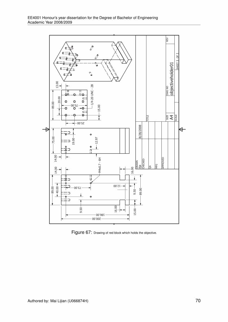
EE4001 Honour’s year dissertation for the Degree of Bachelor of EngineeringAcademic Year 2008/2009
SH
EET 1
O
F 1
DRAW
N
CH
ECKED
QA
MFG
APPRO
VED
ilja
8/2
8/2
008
DW
G N
O
obje
ctiv
ehold
er0
1
TIT
LE
SIZ
E
A4
SCALE
REV
89.0
0
16.0
0
200.00
12.0015.0
0
M4x0.7
- 6
H
75.0
0
40.0
0 73.00
14.0
0
9.5
0
186.00
12.9
7
89.0
0
14.0
0
19.0
0
9.5
0
16.0
0
13.0
0
1/4
-20 U
NC -
2B
20.0
0
25.00
15.0
0
89.0
0 75.00
Figure 67: Drawing of red block which holds the objective.
Authored by: Mai Lijian (U066874H) 70

EE4001 Honour’s year dissertation for the Degree of Bachelor of EngineeringAcademic Year 2008/2009
(0,0)
(7.86,-37.29)
13mm30mm
30mm
40mm
40mm
44.58mm
45.72mm
M3 holes#4-40 holes
(a) Specifications of the heatsink drill holes. (b) Picture of the end result.
Figure 68: LED holder CNC drilling.
Authored by: Mai Lijian (U066874H) 71

EE4001 Honour’s year dissertation for the Degree of Bachelor of EngineeringAcademic Year 2008/2009
B Piezo stage program flowchart
Move to next spot for
course scanning &
echoes data to
command line
Program updates
brightest spot location
New brightest spot
found?
Course Scan
done?
Yes
Moves to next location
for fine scan & echoes
data to command line
Program updates
brightest spot location
Scan done?
New brightest spot
found?Yes
No
No
Positions brightest
spot over microscope
objective
Hold at the same
position and output
holding status to
command line
Spot still bright?
Spot still bright?
Hold for specified
delay timeNo
Yes
Yes
No
Monintor command line
for holding status
message
Holding?No
Collects g(2)(τ) or
spectrum data
Yes
START
Yes
No
Yes
Appends data as part
of tomograph on
screen
Figure 69: Flow chart depicting the operations of the confocal microscope scanning program. Green colour portion controlsthe stage and displays information on screen; programmed in Tcl/Tk. Blue colour portions monitor the command line for signs ofa single molecule being localized and starts collection of data. Programmed in shell script.
Authored by: Mai Lijian (U066874H) 72

Indexp-terphenyl, 8, 47, 61, 63, 64160 mm, 13
Airy disk, 15, 17, 24, 30Airy disk maximum, 16Airy disk minimum, 16Airy disk profile, 15antenna, 8, 64anti-bunched, 4anti-bunched photons, 9, 10APD, 11, 31–34, 55, 63azimuth, 28, 31–33, 45
back focal plane, 19background fluorescence, 50, 57beam-splitter, 9, 31, 32Bessel function, 15blinking, 8, 60, 61Bloch equations, 11Bose-Einstein statistics, 4bosonic bunching, 4
CCD camera, 30, 34, 53, 54, 56, 60, 63chromatic abberation, 20chromatic abberations, 17CIE 1931 curve, 25circular aperture, 15CNC, 36, 38, 63coaxial cable, 30coherent light, 23collimation test, 32colour-centers, 5Colourimetry, 25comatic abberation, 20Commission Internationale de I’Eclairage,
25confocal microscope, 5, 21, 27, 49confocal microscope, illumination, 27confocal microscopy, 21confocal pinhole, 21coverslip, 5, 18, 30, 36, 46–48, 50, 56, 57,
64coverslip correction, 18coverslip thickness, 18coverslips, 46, 47, 56
dark counts, 33, 49, 55dark state, 8dead time, 30dichroic mirror, 22, 28diffraction limit, 15Diffraction limited focusing, 15Diffraction limited resolution, 16dipole moment, 8, 64distortion abberation, 20
effective magnification, 14exitance, 25, 38–40, 50, 56, 57, 60, 61
f-number, 34field number, 17Fischer Scientific coverslips, 56flippable, 28, 34Fluorescent beads, 32, 33, 48, 54, 60, 61focal length, 14, 34folding mirror, 28, 30Fraunhofer diffraction, 15
G-code, 36glass coverslips, 56grids, 35
Hanbury Brown and Twiss, 63Hanbury Brown and Twiss setup, 5, 9, 11,
30, 32high pass filter, 23, 33, 50HOMO, 6, 7
illuminance, 25immersion medium, 15immersion objective, 18immersion oil, 18incoherent light, 5, 23, 24infinity correction, 13intensity, 56, 63interference pattern, 24International Commission on Illumination
1931 Resolutions on Colorimetry,25
interstate excursion, 7intersystem crossing, 7, 12
73
EE4001 Honour’s year dissertation for the Degree of Bachelor of EngineeringAcademic Year 2008/2009
irradiance, 4, 10, 15, 16, 18, 19, 21, 24,25, 28, 30, 32, 49, 52–56, 59, 60,63
Jabłonski energy diagram, 6, 7, 11
Lambert’s cosine law, 41LED, 5, 25, 27, 28, 37–40, 50–54, 56, 58–
60, 63, 71Lumens, lm, 25LUMO, 6, 7Lux, lx, 25
magnification, 13, 14, 20, 30, 34, 35, 39,40
magnification, effective, 14microscope objective, 13–18, 28–30, 35,
36, 55, 60, 61modes, 23, 24mutual coherence function, 23
Nd:YAG, 27, 39, 54, 59number state, 10numerical aperture, 14, 15, 30, 34
objective holder platform, 29objective lens, 13, 19
paraxial rays, 20peak luminous efficacy, 25photometric units, 25photometry, 25piezo stage, 35, 60, 62piezo translation stage, 35Piranha solution, 47PLAN, 17plumbline, 29PMMA/MA, 63, 64point sources, 16, 32polyethylene, 30principal axis, 20, 29, 30
Quantum emitters, 6qubits, 4
radiometric units, 25radiometry, 25rate equations, 11rate of absorption, 12
Rayleigh scattering, 22, 50
SAPO, 17second order correlation function, 10, 12,
30, 58second order correlation function, raw, 30second order correlation, quantum, 10signal to background ratio, 63, 64singlet state population, 12spectrometer, 5, 34, 42, 43, 45, 50, 51spherical abberation, 20Stokes shift, 6superapochromatic, 17
T1 time, 12temporal coherence, 24terrylene, 8, 47–49, 54, 61, 64thermoelectric, 33, 38thin lens, 17timestamp card, 30toluene, 47, 48, 57triplet state, 7, 12triplet state decay rate, 12triplet state population, 12tube lens, 13, 34
UPLANSAPO, 17
visibility, 24
wavelength discrimination, 22wavenumber, 15widefield, 18, 53, 54widefield illumination, 18widefield microscopy, 18
zenith, 28, 31–33, 45zoom objective, 34
Authored by: Mai Lijian (U066874H) 74

EE4001 Honour’s year dissertation for the Degree of Bachelor of EngineeringAcademic Year 2008/2009
List of Figures
1 Jabłonski energy diagram . . . . . . . . . . . . . . . . . . . . . . . . . . 72 Terrylene absorption and emission spectrum . . . . . . . . . . . . . . . 73 Transition dipole moment of a Terrylene molecule in p-terphenyl . . . . 94 Hanbury Brown and Twiss Schematic . . . . . . . . . . . . . . . . . . . 95 Level Scheme used to derive rate equations . . . . . . . . . . . . . . . . 116 Idealized g(2)(τ) . . . . . . . . . . . . . . . . . . . . . . . . . . . . . . . . 127 Labeled microscope objective lens . . . . . . . . . . . . . . . . . . . . . 138 Ray diagram for new and old objectives . . . . . . . . . . . . . . . . . . 149 Diagrams showing physical meaning of NA . . . . . . . . . . . . . . . . 1510 Airy disk profile and picture . . . . . . . . . . . . . . . . . . . . . . . . . 1611 Profiles and picture describing Rayleigh’s resolution . . . . . . . . . . . 1712 Difference between working distance and effective focal length . . . . . 1813 Widefield illumination . . . . . . . . . . . . . . . . . . . . . . . . . . . . . 1914 Widefield image of single molecules . . . . . . . . . . . . . . . . . . . . 1915 Picture of spherical abberation . . . . . . . . . . . . . . . . . . . . . . . 2016 Diagram describing comatic abberation . . . . . . . . . . . . . . . . . . 2017 Picture depicting comatic abberation . . . . . . . . . . . . . . . . . . . . 2018 Picture of objective without distortion abberation . . . . . . . . . . . . . 2119 Picture of objective with distortion abberation . . . . . . . . . . . . . . . 2120 Diagram depicting chromatic abberation . . . . . . . . . . . . . . . . . . 2121 Difference between confocal and conventional microscopy . . . . . . . . 2222 Bare-boned confocal microscope . . . . . . . . . . . . . . . . . . . . . . 2223 Difference between coherent and incoherent focusing . . . . . . . . . . 2324 CIE 1931 curve . . . . . . . . . . . . . . . . . . . . . . . . . . . . . . . . 2525 Schematic of confocal microscope . . . . . . . . . . . . . . . . . . . . . 2726 Picture of microscope alignment path . . . . . . . . . . . . . . . . . . . 2827 Using a plumbline to align microscope . . . . . . . . . . . . . . . . . . . 2928 Raw g(2)(τ) plot . . . . . . . . . . . . . . . . . . . . . . . . . . . . . . . . 3129 Picture of Hanbury Brown and Twiss . . . . . . . . . . . . . . . . . . . . 3130 Fluorescent beads and widefield laser illumination . . . . . . . . . . . . 3331 Picture of Piezo stage and controller . . . . . . . . . . . . . . . . . . . . 3532 Difference between confocal scan and CCD image . . . . . . . . . . . . 3633 Change in setup’s physical layout . . . . . . . . . . . . . . . . . . . . . . 3734 New parts of confocal microscope . . . . . . . . . . . . . . . . . . . . . 3735 Pictures of Luxeon K2 LED . . . . . . . . . . . . . . . . . . . . . . . . . 3836 Pictures of LED holder . . . . . . . . . . . . . . . . . . . . . . . . . . . . 3937 Projection of an small LED die . . . . . . . . . . . . . . . . . . . . . . . 4038 Green LED spectrums . . . . . . . . . . . . . . . . . . . . . . . . . . . . 4139 Pictures of black and white Luxeon Rebel dies . . . . . . . . . . . . . . 4240 Green Rebel LED radiant flux vs input current . . . . . . . . . . . . . . . 4241 spectrometer schematic . . . . . . . . . . . . . . . . . . . . . . . . . . . 4342 Grating first order diffractions . . . . . . . . . . . . . . . . . . . . . . . . 4343 Plot depicting number of steps per spectral nm . . . . . . . . . . . . . . 4544 Reliability test of spectrometer . . . . . . . . . . . . . . . . . . . . . . . 46
Authored by: Mai Lijian (U066874H) 75

EE4001 Honour’s year dissertation for the Degree of Bachelor of EngineeringAcademic Year 2008/2009
45 Picture of spectrometer . . . . . . . . . . . . . . . . . . . . . . . . . . . 4646 Picture of spin coating machine . . . . . . . . . . . . . . . . . . . . . . . 4847 Normalized g(2)(τ) . . . . . . . . . . . . . . . . . . . . . . . . . . . . . . 4948 Spectrum depicting challenge in filtering away illumination light from de-
tection . . . . . . . . . . . . . . . . . . . . . . . . . . . . . . . . . . . . . 5049 Spectrum showing best exciter filter for LED and terrylene . . . . . . . . 5150 Spectrum showing best detector filter for LED and terrylene . . . . . . . 5151 Spectrum non ideal filters in the lab . . . . . . . . . . . . . . . . . . . . . 5252 Spectrum showing a more efficient overlap of LED with terrylene com-
pared to laser illumination . . . . . . . . . . . . . . . . . . . . . . . . . . 5353 Measurement of widefield illumination . . . . . . . . . . . . . . . . . . . 5354 Measuring LED irradiance on sample . . . . . . . . . . . . . . . . . . . 5555 Picture of LED imaged onto Fluorescent beads . . . . . . . . . . . . . . 5556 Signal to background ratio of widefield illumination by both laser and LED 5757 Pictures of LED and laser illuminated fluorescent samples. . . . . . . . 5758 Picture showing confocal scan . . . . . . . . . . . . . . . . . . . . . . . 5859 Ideal filter . . . . . . . . . . . . . . . . . . . . . . . . . . . . . . . . . . . 5960 Diagram depicting spatial filtering . . . . . . . . . . . . . . . . . . . . . . 6061 Bleaching trend . . . . . . . . . . . . . . . . . . . . . . . . . . . . . . . . 6162 GUI of piezo stage controller . . . . . . . . . . . . . . . . . . . . . . . . 6163 Transition dipole moment of a Terrylene molecule in PMMA/MA . . . . . 6464 Drawing of sample fork . . . . . . . . . . . . . . . . . . . . . . . . . . . . 6765 Drawing of adapter . . . . . . . . . . . . . . . . . . . . . . . . . . . . . . 6866 Drawing of scanner block holder . . . . . . . . . . . . . . . . . . . . . . 6967 Drawing of objective holder . . . . . . . . . . . . . . . . . . . . . . . . . 7068 Drawing of LED holders . . . . . . . . . . . . . . . . . . . . . . . . . . . 7169 Flowchart of program controlling piezo stage . . . . . . . . . . . . . . . 72
Authored by: Mai Lijian (U066874H) 76

EE4001 Honour’s year dissertation for the Degree of Bachelor of EngineeringAcademic Year 2008/2009
List of Tables
1 Table of LEDs tested . . . . . . . . . . . . . . . . . . . . . . . . . . . . . 402 Table of exitance per FWHM of spectral width . . . . . . . . . . . . . . . 41
Authored by: Mai Lijian (U066874H) 77

EE4001 Honour’s year dissertation for the Degree of Bachelor of EngineeringAcademic Year 2008/2009
References
[1] Charles H. Bennett and Gilles Brassard. Quantum cryptography: Public key dis-tribution and coin tossing. Proceedings of the IEEE International Conference onComputers, Systems, and Signal Processing, page 175, 1984.
[2] Artur K. Ekert. Quantum cryptography based on Bell’s theorem. Phys. Rev. Lett.,67(6):661–663, Aug 1991.
[3] Brahim Lounis and Michel Orrit. Single-photon sources. Reports on Progress inPhysics, 68(5):1129–1179, 2005.
[4] Hans A. Bachor and Timothy C. Ralph. A Guide to Experiments in QuantumOptics. Wiley-VCH, 2004.
[5] Alexander Ling, Matt Peloso, Ivan Marcikic, Antıa Lamas-Linares, and Chris-tian Kurtsiefer. Experimental E91 quantum key distribution. Proc. of SPIE,6903:69030U–1, 2008.
[6] Eugene Hecht. Optics. Addison Wesley, 2002.
[7] Charles Santori, David Fattal, and Jelena Vuckovicand Glenn S. Solomon& Yoshihisa Yamamoto. Indistinguishable photons from a single-photon device.Nature, 419:594–597, 2002.
[8] Peng Jin-Sheng and Li Gao-Xiang. Introduction to Modern Quantum Optics.World Scientific, 1998.
[9] Brahim Lounis and W.E Moerner. Single photons on demand from a singlemolecule at room temperature. Nature, 407:491–493, Sept 2000.
[10] Christian Kurtsiefer, Sonja Mayer, Patrick Zarda, and Harald Weinfurter. Stablesolid-state source of single photons. Phys. Rev. Lett., 85(2):290–293, Jul 2000.
[11] T. Gaebel, I. Popa, A. Gruber, M. Domhan, F. Jelezko, and J. Wrachtrup. Stablesingle -photon source in the near infrared. New Journal of Physics, 6:98, 2004.
[12] Jason S. Kuo, Christopher L. Kuyper, Peter B. Allen, Gina S. Fiorini, and Daniel T.Chiu. High-power blue/UV light-emitting diodes as excitation sources for sensitivedetection. Electrophoresis, 25:3796–3804, 2004.
[13] M. Unger, E.Kartalov, C.-S. Chiu, H.A. Lester, and S.R. Quake. Single-moleculefluorescence observed with mercury lamp illumination. BioTechniques, 27:1008–1014, Nov. 1999.
[14] V. Jacques, J.D Murray, F. Marquier, D. Chauvat, F. Grosshans, F. Treussart, andJ.-F. Roch. Enhancing single-molecule photostability by optical feedback fromquantum jump detection. Applied Physics Letters, 93, Nov. 2008.
[15] W.E. Moerner. Single-photon sources based on single molecules in solids. NewJournal of Physics, 6:88, 2004.
Authored by: Mai Lijian (U066874H) 78

EE4001 Honour’s year dissertation for the Degree of Bachelor of EngineeringAcademic Year 2008/2009
[16] F. Kulzer, F. Koberling, Th. Christ, A. Mews, and Th. Basch. Terrylene in p-terphenyl: single-molecule experiments at room temperature. Chemical Physics,247(Issue 1):23–34, August 1999.
[17] Bert Hecht and Lukas Novotny. Principles of Nano-Optics. Cambridge UniversityPress, 2006.
[18] Brian Herman, Victoria E. Centonze Frohlich, Joseph R. Lakowicz, Douglas B.Murphy, Kenneth R. Spring, and Michael W. Davidson. Olympus microscopy re-source center, fluorescence microscopy, basic concepts in fluorescence.
[19] S.P. McGlynn, T. Azumi, and M. Kinoshita. Molecular Spectroscopy of the tripletstate. Prentice-Hall, 1969.
[20] Christian Florian Seebacher. Einzelmolekulspektroskopie von organischen Farb-stoffmolekulen in porosen Festkorpern und Tieftemperaturspektroskopie an demgrun fluoreszierenden Protein. PhD thesis, Ludwig-Maximilians-UniversitatMunchen, 2002.
[21] Oliver Panzer, Wolfgang Ghde, Ulrich C. Fischer, Harald Fuchs, and Klaus Mullen.Influence of oxygen on single molecule blinking. Advanced materials, 10(Issue17):1469–1472, December 1998.
[22] A. Nicolet, M. A. Kol’chenko, B. Kozankiewicz, and M. Orrit. Intermolecular inter-system crossing in single-molecule spectroscopy: Terrylene in anthracene crys-tal. The Journal of Chemical Physics, 124:164711, 2006.
[23] S. Kummer, F. Kulzer, R. Kettner, Th. Basch, C. Tietz, C. Glowatz, and C. Kryschi.Absorption, excitation, and emission spectroscopy of terrylene in p-terphenyl:Bulk measurements and single molecule studies. The Journal of ChemicalPhysics, 107(19):7673–7684, 1997.
[24] R.J. Pfab, J. Zimmermann, C. Hettich, I. Gerhardt, A. Renn, and V. Sandogh-dar. Aligned terrylene molecules in a spin-coated ultrathin crystalline film of p-terphenyl. Chemical Physics Letters, 387:490–495, 2004.
[25] R. Q. Twiss, A. G. Little, and R. Hanbury Brown. Correlation between photons, incoherent beams of light, detected by a coincidence counting technique. Nature,180:324–326, August 1957.
[26] Rodney Loudon. The quantum theory of light. Oxford University Press, 3rd edi-tion, 2000.
[27] K Sam Wells, David R. Sandison, James Strickler, and Watt W. Webb. Quanti-tative fluorescence imaging with laser scanning confocal microscopy, chapter 3,pages 27–39. Plenum Press, 1990. Handbook of biological confocal microscopy.
[28] http://www.spachoptics.com/v/vspfiles/photos/uplsapo-100-2t.jpg. Picture.
[29] Maksymilian Pluta. Advanced Light Micrscopy, volume 1. Elsevier, 1988.
Authored by: Mai Lijian (U066874H) 79

EE4001 Honour’s year dissertation for the Degree of Bachelor of EngineeringAcademic Year 2008/2009
[30] I. Shinya. Foundations of confocal scanned imaging in light microscopy, chap-ter 1, pages 1–13. Plenum Press, 1990. Handbook of biological confocal mi-croscopy.
[31] http://www.microscopyu.com/tutorials/java/virtual/confocal/.
[32] Commission Internationale de l’Eclairage proceedings. Cie 1931 standard colori-metric observer y2(lambda) data (between 380 nm and 780 nm at 5 nm intervals),1932.
[33] Jnos Schanda. Colorimetry: Understanding the CIE system, chapter 3, pages25–76. Wiley-Interscience, 2007.
[34] Henri Dautet, Pierre Deschamps, Bruno Dion, Andrew D. MacGregor, DarleeneMacSween, Robert J. McIntyre, Claude Trottier, and Paul P. Webb. Photoncounting techniques with silicon avalanche photodiodes. Applied Optics, 32(No.21):3894, July 1993.
[35] Perkin-Elmer. Silicon avalanche photodiodes c30902 series technical datasheet.
[36] Bahaa E.A. Saleh and Malvin Carl Teich. Fundamentals of Photonics. Wiley-Interscience, 2nd edition edition, 2007.
[37] Max Born and Emil Wolf. Principles of Optics. Cambridge University Press, 7th(expanded) edition, 2002.
[38] Richard Young. Measuring light emission from leds. Advanced LEDs for SolidState Lighting, Proceedings of SPIE, 6355:63550H–1, 2006.
[39] Daniel Zwillinger. CRC Standard Mathematical Tables and Formulaes. CRCPress, Chapham & Hall, 31th edition, 2003.
[40] Edge filter spectra vs. angle of incidence, semrock inc. technical notes.
[41] Andrew H. Fischer, Kenneth A. Jacobson, Jack Rose, and Rolf Zeller. Preparationof slides and coverslips for microscopy. Cold Spring Habour Protocols, 2008.
Authored by: Mai Lijian (U066874H) 80