about the arm processor - egloospds9.egloos.com/pds/200803/19/35/about_the_arm_processor.pdf ·...
TRANSCRIPT


ARM LtdFounded in November 1990
Spun out of Acorn Computers
Designs the ARM range of RISC processor cores
Licenses ARM core designs to semiconductor partners who fabricate and sell to their customers
ARM does not fabricate silicon itself
Also develop technologies to assist with the design-in of the ARM architecture
Software tools, boards, debug hardware, application software, bus architectures, peripherals etc

ARM HISTORY(1985 – 1995)1985
Acorn Computer Group develops the world's first commercial RISC processor 1987
Acorn's ARM processor debuts as the first RISC processor for low-cost PCs 1990
Advanced RISC Machines (ARM) spins out of Acorn and Apple Computer's collaboration efforts with a charter to create a new microprocessor standard. VLSI Technology becomes an investor and the first licensee
1993ARM introduces the ARM7™ core
1994Samsung license ARM technology ARM introduces the ARM7500™ "system-chip" for multimedia applications
1995ARM's Thumb® architecture extension gives 32-bit RISC performance at 16-bit system cost and offers industry-leading code density ARM launches Software Development Toolkit First StrongARM™ core from Digital Semiconductor and ARM ARM extends family with ARM8™ high-performance solution ARM launches the ARM7100™ "PDA-on-a-chip“
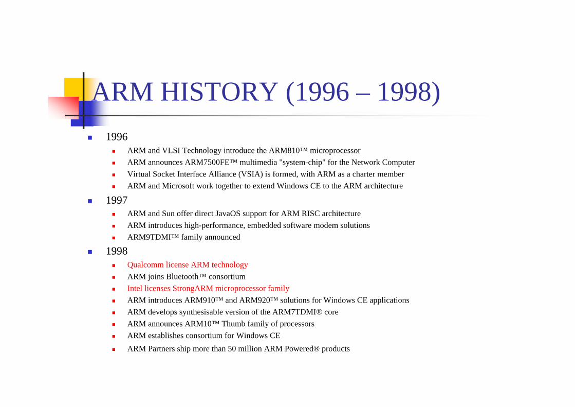
ARM HISTORY (1996 – 1998)1996
ARM and VLSI Technology introduce the ARM810™ microprocessor ARM announces ARM7500FE™ multimedia "system-chip" for the Network Computer Virtual Socket Interface Alliance (VSIA) is formed, with ARM as a charter member ARM and Microsoft work together to extend Windows CE to the ARM architecture
1997ARM and Sun offer direct JavaOS support for ARM RISC architecture ARM introduces high-performance, embedded software modem solutions ARM9TDMI™ family announced
1998Qualcomm license ARM technologyARM joins Bluetooth™ consortium Intel licenses StrongARM microprocessor familyARM introduces ARM910™ and ARM920™ solutions for Windows CE applications ARM develops synthesisable version of the ARM7TDMI® core ARM announces ARM10™ Thumb family of processorsARM establishes consortium for Windows CE ARM Partners ship more than 50 million ARM Powered® products

ARM HISTORY (1999 – 2001)1999
ARM announces synthesisable ARM9E™ processor with enhanced signal processingARM works with Microsoft to optimize Windows Media Audio ARM introduces MP3 and Dolby Digital Software solutions
2000ARM launches SecurCore™ family for smartcards ARM introduces Jazelle™ technology for Java™ applications ARM introduces ARM922T™ core Lucent ships ARM10™ silicon ARM supports Intel's launch of ARM architecture-compliant XScale™ microarchitecture
2001ARM announces new ARMv6 architecture ARM announces the ARM VFP9-S™ and ARM VFP10™ vector floating-point coprocessors ARM introduces the ARM926EJ-S™ soft macrocell, the ARM7EJ™ core, and the Jazelle Technology Enabling Kit™ (JTEK)SavaJe and Symbian license Jazelle™ software for incorporation into their operating systemsARM announces the PrimeXsys™ platforms. ARM introduces the SecurCore SC200™ and SC210™ microprocessor cores ARM announces MOVE™ multimedia acceleration technology for wireless devices

ARM PARTNER

ARM POWERED PRODUCTS

ARM FEATURERISC(Reduced Instruction Set Computer) architectureGeneral purpose 32-bit microprocessorsVery low power consumption and priceBig/Little Endian Mode
Intel x86 – Little EndianMotorola – Big Endian
Fast Interrupt ResponseFIQ Mode
Excellent High Level Language Support C Language Auto Increment/Decrement addressing mode
Simple and powerful Instruction SetLoad/Store multiple instructionsConditional execution

ARM ARCHITECTURE
XXXXV6
XXXV5TEJ
XXV5TE
XV4T
MediaJazelleDSPTHUMBArchitecture

ARM ARCHITECTUREv4T
Thumb instruction set Short 16-bit instructionsTypical memory savings of up to 35%
5TEDSP instruction set 70% speed up(audio DSP applications)
v5TEJJazelle technology for java 80% reduction
V6SIMD extensions
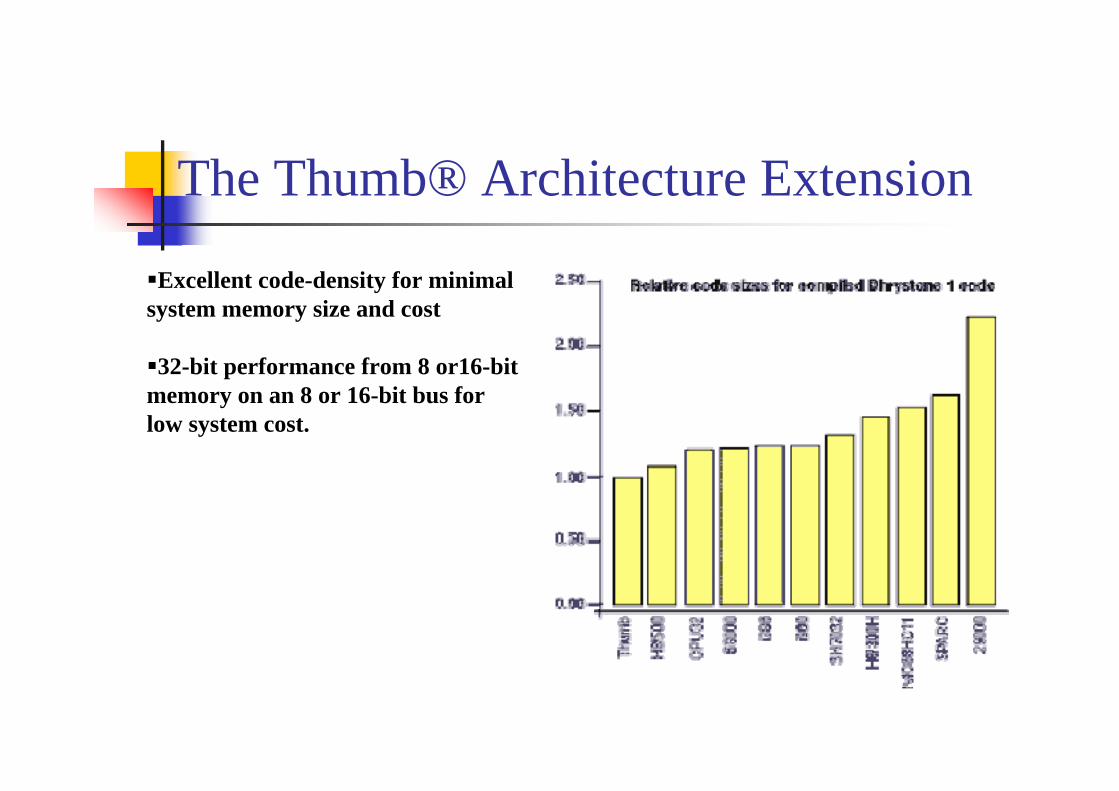
The Thumb® Architecture Extension
Excellent code-density for minimal system memory size and cost
32-bit performance from 8 or16-bit memory on an 8 or 16-bit bus for low system cost.
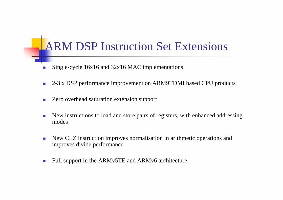
ARM DSP Instruction Set ExtensionsSingle-cycle 16x16 and 32x16 MAC implementations
2-3 x DSP performance improvement on ARM9TDMI based CPU products
Zero overhead saturation extension support
New instructions to load and store pairs of registers, with enhanced addressing modes
New CLZ instruction improves normalisation in arithmetic operations and improves divide performance
Full support in the ARMv5TE and ARMv6 architecture

ARM® Jazelle TechnologyThe ARM Jazelle technology provides a highly-optimized implementation of the Java Virtual Machine (JVM), speeding up execution times and providing consumers with an enriched user experience on their mobile devices.,

ARM Media ExtensionsOverview
•streaming media performance (film, video phone, music and more), •more human-oriented interfaces (voice and handwriting recognition)
Feature•2-4x performance increase for audio and video processing •Simultaneous computation of 2x16-bit or 4x8-bit operands •Fractional arithmetic •User definable saturation modes (arbitrary word-width) •Dual 16x16 multiply-add/subtract •32x23 fractional MAC •Simultaneous 8/16-bit select operations

THE ARM CORE FAMILY- ROADMAP
V4T V5TEJV5TE V6
ARM7 Securecore
ARM9
ARM10E/EJ
ARM1136J(F)-S
ARM9E/EJ
Xscale
100 MIPS(<50mW)
200-300 MIPS (<160mW)
400-900 MIPS(150-825mW)
400-550 MIPS+DSP
(<300mW)200-300 MIPS
+DSP(<300mW)
400MIPS
Perf
orm
ance
ROADMAP
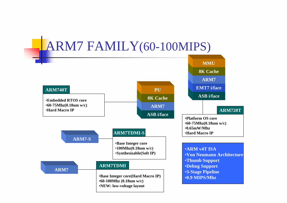
ARM7 FAMILY(60-100MIPS)
ASB i/face
ARM7
8K Cache
PUASB i/face
EMT7 i/face
ARM7
8K Cache
MMU
ARM7
ARM7-S
ARM7TDMI
ARM740T
ARM7TDMI-S
ARM720T
•Embedded RTOS core•60-75Mhz(0.18um w/c)•Hard Macro IP
•ARM v4T ISA•Von Neumann Architecture•Thumb Support•Debug Support•3-Stage Pipeline•0.9 MIPS/Mhz
•Platform OS core•60-75Mhz(0.18um w/c)•0.65mW/Mhz•Hard Macro IP
•Base Integer core(Hard Macro IP)•60-100Mhz (0.18um w/c)•NEW: low-voltage layout
•Base Integer core•100Mhz(0.18um w/c)•Synthesizable(Soft IP)

ARM9 FAMILY(200 MIPS)
ASB i/face
ARM9T
4K Caches
PU
ASB i/face
EMT7 i/face
ARM9T
16K Caches
MMU
ARM9T
ARM920T
•Hard macro IP•ARM v4T ISA•Harvard architecture•Thumb Support•Debug Support•5-Stage Pipeline•Dual Caches•AMBA ASB bus•1.1 MIPS/Mhz
•Platform OS processor core•Up to 200Mhz(0.18um w/c) •0.8mW/Mhz
ASBi/face
EMT9 i/face
ARM9
8K Cache
MMU
ARM940T
•Embedded RTOS processor core•Up to 180Mhz(0.18um w/c) •0.85mW/Mhz
ARM9TDMI
•Base Integer processor core•Up to 220Mhz(0.18um w/c)•0.3mW/Mhz
ARM922T
•Platform OS processor core•Up to 200Mhz(0.18um w/c) •0.8mW/Mhz

ARM9E FAMILY(200 MIPS+DSP)
AHB i/face
ETM9 i/face
ARM9E-S
Flexible SRAMs
AHB i/face
EMT7 i/face
ARM9E-S
Flexible Caches
TCM i/face
ARM9E-S
ARM926EJ-S
•Synthesizable (Soft IP)•ARM v5TE ISA•Thumb Support•Debug Support•5-Stage Pipeline•Dual Caches•AMBA AHB bus
•Platform OS processor core•200MIPS(0.18um w/c target•~190K gates + SRAM
AHB i/face
EMT9 i/face
ARM9E-S
Flexible Caches
TCM i/face
ARM966E-S
•Embedded processor core•180MIPS(0.18um w/c) •~110K gates + SRAM
ARM9E-S
ARM946E-S
•Embedded OS processor core•160MIPS(0.18um w/c) •~140K gates + SRAM
PUMMU
Jazelle™Enhanced
•Base Integer processor core•180MIPS(0.18um w/c) •~65K gates

ARM10E FAMILY(390 MIPS+DSP)
Dual AHB
EMT10 i/face
ARM10E
2x16K Cache
MMU
Dual AHB
EMT10 i/face
ARM10J
16K/32K Cache
MMU
Dual AHB
EMT10 i/face
ARM10E
2x32K Cache
MMU
ARM946E-S
•Platform OS core•300Mhz(0.15um w/c)•Hard Macro IP
VFP10
Jazelle™Enhanced
•ARM v5TE ISA•Thumb Code Compression•Debug Support•6-Stage Pipeline•Dual Cache architecture•Dual 64-bit AHB bus•Optional VFP coprocessor•AMBA AHB bus•1.3 MIPS/Mhz•Low power: 0.7mW/MIPS
ARM1020E
•Platform OS core•300Mhz(0.15um w/c)•Hard Macro IP
ARM966E-S•Platform OS core•>400Mhz(0.13um w/c)•Hard Macro IP
ARM966E-S•600Mflops Vector floatingPoint coprocessor

ARM11 FAMILY(<400 MIPS+DSP+ Jazelle™)
M-layer AHB
M-layer AHB
ARM11
ARM1136J-S
•Platform OS core•Up to 1Ghz(0.15um w/c)
•ARM v6 ISA•Thumb Code Compression•DSP extensions•8-Stage Pipeline( 35% enhanced)•SIMD media processing•Multi-port 64bit memory system•Optional VFP coprocessor•TCM(scratch-pad) memory•Low power: 0.4mW/Mhz
ARM11
•Platform OS core•Up to 1Ghz(0.15um w/c)
ARM1136JF-S•Platform OS core•600Mflops Vector floating•Point coprocessor
Multi Port
ARM11
I/D Cache
TCM
Multi Port
ARM11
I/D Cache
TCM
VFP

SA Core
DRAM
16K I/D Cache
MMU
SA1100
•199Mhz
•SA core(StrongARM)•ARM8 •ARM v4 Architecture•Harvard Architecture ,I/D Cache•5-Stage Pipeline
•Xscale•ARM5T Architecture•Thumb mode Support•7-stage integer, 8-stage memory superpipeline
SA110
•Up to 233Mhz•Only Core Support
PXA210(250)
•Up to 400Mhz
INTEL SA & XSCALE FAMILY
SDRAM
SA1110
•206Mhz
SA Core
DRAM
16K I-Cache
8K-D-Cache
MMU
Xcale Core
64-bit BIU
2K Mini/D Cache
32K I/D Cache
I/D MMU

ARM PROCESSOR CORES
200
400
100
Un-cached CoresFor
Hard real-timerApplications
ARM1136(J)-S ARM1136(J)-SARM1020E
MIPS
ARM9TDMIARM9E-S
ARM7TDMIARM7TDMI-S
ARM966E-S ARM940TARM946E-S
ARM740T
ARM920TARM926E-S
ARM720T
Basic Cores
Cached Cores With
Embedded real-time
applications
Cached CoresWith full MMU
OSSupport for e.g.
winCE ,Symbian OS,
Linux

ARM7TDMI Core diagram

ARM INSTRUCTIONS
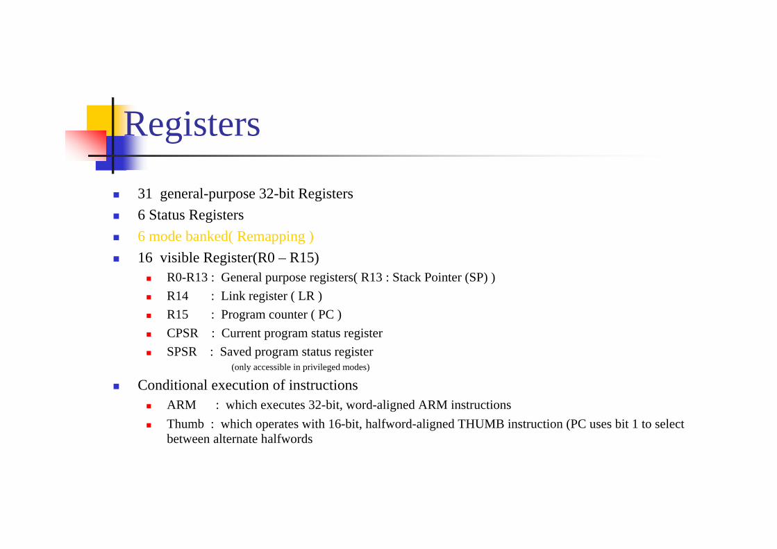
Registers
31 general-purpose 32-bit Registers6 Status Registers6 mode banked( Remapping )16 visible Register(R0 – R15)
R0-R13 : General purpose registers( R13 : Stack Pointer (SP) )R14 : Link register ( LR )R15 : Program counter ( PC )CPSR : Current program status registerSPSR : Saved program status register
(only accessible in privileged modes)
Conditional execution of instructionsARM : which executes 32-bit, word-aligned ARM instructionsThumb : which operates with 16-bit, halfword-aligned THUMB instruction (PC uses bit 1 to select between alternate halfwords

Program Status Register Format
M0
M1
M2
M3
M4
TFIVCZN31 30 29 28 27 8 7 6 5 4 3 2 1 0
Condition Code Flags Reserved Control Bits
Condition Code Flags( arithmetic and logical operations)N : Negative/Less ThanZ : ZeroC : Carry/Borrow/ExtendV : Overflow
Control bitsI : IRQ disable (Active Set)F : FIQ disable (Active Set)T : State bit ( 1: Thumb state 0: ARM state)Mode bits
User, FIQ, IRQ, Supervisor, Abort, Undefined

Processor Modes
Runs privileged operating system tasks 1111System( sys )
Supports software emulation of hardware coprocessors11011Undefined( und )
Implements virtual memory and/or memory protection10111Abort( abt )
A protected mode for the operating system10011Supervisor( svc)
Used for general purpose interrupt handling10010IRQ( irq )
Supports a high-speed data transfer or channel process10001FIQ( fiq )
Normal program execute mode10000User( usr )
DescriptionValueM[4:0]Mode
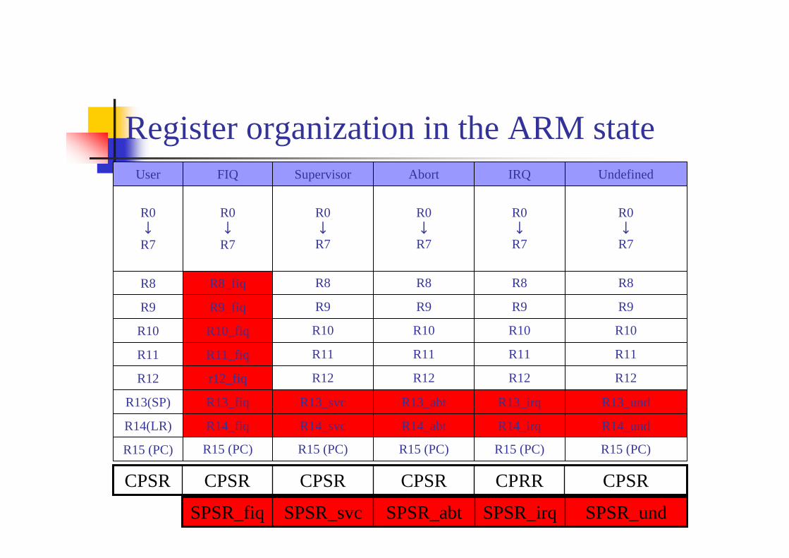
Register organization in the ARM state
R15 (PC)R15 (PC)R15 (PC)R15 (PC)R15 (PC)R15 (PC)
R14_undR14_irqR14_abtR14_svcR14_fiqR14(LR)
R13_undR13_irqR13_abtR13_svcR13_fiqR13(SP)
R12R12R12R12r12_fiqR12
R11R11R11R11R11_fiqR11
R10R10R10R10R10_fiqR10
R9R9R9R9R9_fiqR9
R8R8R8R8R8_fiqR8
R0↓R7
R0↓R7
R0↓R7
R0↓R7
R0↓R7
R0↓R7
UndefinedIRQAbortSupervisorFIQUser
CPSRCPRRCPSRCPSRCPSRCPSR
SPSR_undSPSR_irqSPSR_abtSPSR_svcSPSR_fiq

Register organization in the Thumb state
PCPCPCPCPCPC
LR_undLR_irqLR_abtLR_svcLR_fiqLR
SP_undSP_irqSP_abtSP_svcSP_fiqSP
Not UsedR8↓
R12
R0↓R7
R0↓R7
R0↓R7
R0↓R7
R0↓R7
R0↓R7
UndefinedIRQAbortSupervisorFIQUser
CPSRCPRRCPSRCPSRCPSRCPSR
SPSR_undSPSR_irqSPSR_abtSPSR_svcSPSR_fiq

Exception
Interrupts, traps, supervisor calls
Exceptions arise whenever the normal flow of program has to be halted temporarily

CISC and RISC
CISC (Complex Instruction Set Computing) 구조단순한 명령 처리에서 복합적인 명령 수행까지 하나의 명령집합으로 실행할 수 있도록 여러 개의 명령어를 가진구조논리 회로 증가→명령어마다 실행속도가 틀리다과다한 Memory Access로 속도 저하
RISC (Reduced Instruction Set Computing) 구조1975년 IBM 왓슨 연구소의 John Cocke명령의 종류를 최소한으로 줄임→논리회로 줄어듬여러 개의 명령을 여러 개의 연산회로에 나누어 처리파이프 라인 구조 채택
Pt = Ti + 2Ti + 3Ti+ … + nTi
(Pt : 프로그램 실행 시간, Ti : 명령어의 실행시간, n : 명령어의 수)Ti를 줄이자 RISCN을 줄이자 CISC

Interrupt Concept Hardware Interrupt
외부의 사건을 CPU에게 알리는 방편
인터럽트가 걸리면 CPU가 자동으로 반응하게 됨
의의 - CPU가 실행중인 프로그램의 영향에서 벗어나게 함.
Software Interrupt 프로그램에서 명령에 의해 실행됨
동작방법은 하드웨어 인터럽트와 유사함
Interrupt 서비스루틴 - 모든 program이 공유. kernel level의 프로그램
입출력 연산을 한 군데서 제어하는데 유용함입출력 장치로부터의 사건발생(키보드, 마우스, 디스크 등)비정상적인 긴급한 상황의 발생 (전원 고장,등) 불법 명령의 수행 금지( 0 으로 나누기, 없는 명력 수행 시도 등)
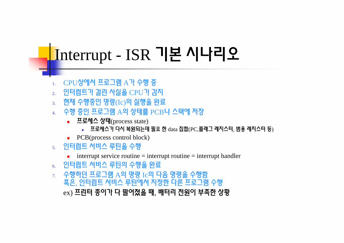
Interrupt - ISR 기본 시나리오
1. CPU상에서 프로그램 A가 수행 중2. 인터럽트가 걸린 사실을 CPU가 감지3. 현재 수행중인 명령(Ic)의 실행을 완료4. 수행 중인 프로그램 A의 상태를 PCB나 스택에 저장
프로세스 상태(process state)프로세스가 다시 복원되는데 필요 한 data 집합(PC,플래그 레지스터, 범용 레지스터 등)
PCB(process control block) 5. 인터럽트 서비스 루틴을 수행
interrupt service routine = interrupt routine = interrupt handler 6. 인터럽트 서비스 루틴의 수행을 완료7. 수행하던 프로그램 A의 명령 Ic의 다음 명령을 수행함
혹은, 인터럽트 서비스 루틴에서 지정한 다른 프로그램 수행ex) 프린터 종이가 다 떨어졌을 때, 배터리 전원이 부족한 상황

Interrupt - 용어
Interrupt sourceInput pin, counter, Serial port 등과 같이 Interrupt를 발생시킬 수있는 것들
Interrupt vectorInterrupt 발생시 분기 장소(Address)
Interrupt service routine(ISR)실제 Interrupt 처리 프로그램
Interrupt priority인터럽트가 동시에발생 할 때, 어떤 인터럽트를 먼저 처리할 것인가를 결정하는 것
Interrupt priority가 높은 것이 낮은 것보다 먼저 발생한다

Exception Vector
3
4
2
5
6
6
1
Priorities
FIQ
IRQ
Abort
Abort
Supervisor
Undefined
Supervisor
Mode on entry
The FIQ exception is a fast interrupt caused by a Low level on the nFIQ input . R8 – R14 remappedFIQ0x0000001C
The IRQ exception is a normal interrupt caused by a Low level on the nIRQinput. R13 – R14 remapped
IRQ0x00000018
Reserved 0x00000014
Abort (Data)0x00000010When the current memory access cannot be
completedAbort (Pre-fetch)0x0000000C
Software Program Interrupt.System callSoftware Interrupt0x00000008
When ARM comes across an undefined instruction
UndefinedInstruction0x00000004
When the nRESET signal goes LOWReset0x00000000
DescriptionExceptionAddress

Exception Flow – ResetnReset
R14_svc = PCSPSR_svc = CPSR
M [4:0] = 10011IRQ Mode ( M[4:0] = 10010 )ARM state ( T = 0 )FIQ Disable ( F = 1 )IRQ Disable ( I = 1 )
PC = 0x00
ARM State
Reset Exception Flow
Supervisor Mode Enter
Reset Vector Branch
Next Instruction fetch
Fetch
R13_svc = Unpredictable valueR14_svc = Unpredictable value

Exception Flow – IRQ
IRQ Event
User Mode(R0-R15)
PC → 0x18
Exit
IRQ Exception Flow
IRQ Service Routineexecution
SPSR_irq→ CPSR
IRQ Exception Entry IRQ Exception Exit
User Mode(R0-R15)
R14_irq → PC
IRQ Vector Branch
User Mode
User Branch
IRQ SR Exit
IRQ SR Entry
IRQ Exception Entry
R13 to R13_irqR14 to R14_irq
Register Remapping
CPSR → SPSR_irqIRQ Mode ( M[4:0] = 10010 )ARM state ( T = 0 )IRQ Disable ( I = 1 )
IRQ Mode
( PC + 4 ) → R14_irq Return Address
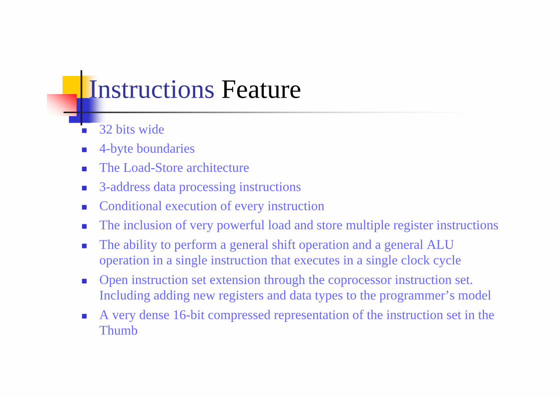
Instructions Feature32 bits wide 4-byte boundariesThe Load-Store architecture 3-address data processing instructionsConditional execution of every instructionThe inclusion of very powerful load and store multiple register instructionsThe ability to perform a general shift operation and a general ALU operation in a single instruction that executes in a single clock cycleOpen instruction set extension through the coprocessor instruction set. Including adding new registers and data types to the programmer’s modelA very dense 16-bit compressed representation of the instruction set in the Thumb

Instruction Format
Instruction Operation
ADD R1, R2, R3 ; R1: = R2 + R3
Operator DestinationRegister(Rd)
Source Register(Rn)Operand 1
Source Register(Rs)Operand 2
Comment Result
Note:1) Operand 1 is always a register2) Operand 2 can be a register or an immediate value

Branch Instruction(B , BL)
[31:28] Cond : Condition Field
[27:25] 101 : B instruction
[24] L bit 0 – Branch( B)1 – Branch with Link (BL)
[23:0] Offset A singed 2’s complement 24 bit offset Branches beyond +/- 32Mbytes ( Because PC increases 2 words (8 bytes)
ExamplesB label ; branch unconditionally to labelBCC label ; branch to label if carry flag is clearBEQ label ; branch to label if zero flag is setMOV PC, #0 ; R15 = 0, branch to location zeroBL func ; subroutine cal to function
func MOV PC, LR ; R15 = R14, return to instruction after the BLMOV LR, PC ; store the address of the instruction after the next one into R14 ready to
; returnLDR PC, =func ; load a 32-bit value into the program counter
OffsetL101Cond
31 28 27 26 25 24 23 0
Data Processing Instructions Format
Rn00 Operand 2RdSOpcodeICond
31 28 27 26
[31:28] Cond : Condition Field[25] I : Immediate Operand
0 : Operand 2 is Register1 : Operand 2 is an immediate value
[24:21] Opcode : Operation Codes ( Data Processing Instruction )[20] S : Set condition codes( CPSR effect )
0 : Do not after condition codes1 : Set condition codes
[19:16] Rn : Source Register Operand 1 (always Register)[15:12] Rd: Destination Register [11:0] Operand 2 : Operand 2 type selection
25 24 21 20 19 16 15 12 11 0
[11:0] Operand 2 : Operand 2 type selection
RmShiftImmRotate
1: immediate value0: Register
11 4
11 8
3 0
7 0
[11:4] Shift : Shift applied to Rm[3:0] Rm 2nd Operand register
Count 0Type 0Rs 1Type
11 7 11 86 5 4 7 6 5 4
Shift Operation
[11:7] Shift amount 5 bit unsigned integer
[6:5] Shift type
[11:7] Shift registerShift amount specified inBottom-byte of Rs
[6:5] Shift type
RORRotate right 11
ASRArithmetic right10
LSRLogical right01
LSLLogical left00
MnemonicInstructionValue
Shift Type Operation
[11:8] RotateShift applied to Imm[7:0]Unsigned 8 bit immediate value
•8 bit immediate value is zero extendedto 32 bits,And then subject to a rotate right by twice the value In the rotate field
ALU
Barrel Shifter
Rd
Op1( Rn ) Operand2

Shift Operations
00000
31 0
00000
31 0
0
00000 0
31 0
31 0
LSL #5 LSR #5
11111 1
ASR #5, positive operand
ROR #5ASR #5, negative operand

[24:21] Opcode : Operation Codes
Rd: = NOT Op2Move NotMVN1111
Rd: Op1 AND (NOT Op2)Bit ClearBIC1110
Rd: = Op2Mov register or constantMOV1101
Rd: = Op1 OR Op2Logical (inclusive) ORORR1100
Op1 + Op2→ CPSRCompare NegativeCMN1011
Op1 – Op2 → CPSRCompareCMP1010
Op1 XOR OP2 → CPSRTest bitwise equalityTEQ1001
Op1 AND OP2 → CPSRTest bitsTST1000
Rd: = Op2 – Op1 + C – 1Reverse Subtract with carryRSC0111
Rd: = Op1 – Op2 + C – 1Subtract with carrySBC0110
Rd: = Op1 + Op2 + CAdd with carryADC0101
Rd: = Op1 + Op2AddADD0100
Rd: = Op2 – Op1Reverse SubtractRSB0011
Rd: = Op1 – Op2SubtractSUB0010
Rd: = Op1 XOR Op2ExclusiveEOR0001
Rd : = Op1 And Op2ANDAND0000
ActionOperationMnemonicOpcode

Condition Code SummaryMeaningFlagsSuffixCode
Always( Ignored )AL1110
less than or equalZ Set or N Set and V Clear or N Clear and V SetLE1101
greater thanZ Clear and ether N Set and V Set or N Clear and V ClearGT1100
less thanN Set and V Clear or N Clear and V SetLT1011
greater or equalN Set and V Set o N Clear and V ClearGE1010
unsigned lower or sameC Clear or Z SetLS1001
unsigned higherC Set and Z ClearHI1000
no overflowV ClearVC0111
overflowV SetVS0110
positive or zeroM ClearPL0101
negativeN SetMI0100
unsigned lowerC ClearCC0011
unsigned higher or sameC setCS0010
not equalZ ClearNE0001
equalZ SetEQ0000

Data Processing Instruction Summary (1)
Arithmetic operationsADD R0, R1, R2 ; R0: = R1 + R2ADC R0, R1, R2 ; R0: = R1 +R2 + C SUB R0, R1, R2 ; R0: = R1 – R2SUC R0, R1, R2 ; R0: = R1 – R2 +C -1RSB R0, R1, R2 ; R0: = R2 – R1RSC R0, R1, R2 ; R0: = R2 – R1 + C –1
Bit-wise logical Operations AND R0, R1, R2 ; R0: = R1 and R2ORR R0, R1, R2 ; R0: = R1 or R2EOR R0, R1, R2 ; R0: = R1 xor R2BIC R0, R1, R2 ; R0: = R1 and not R2
Register movement operationsMOV R0, R2 ; R0: = R2MVN R0, R2 ; R0: = not R2

Data Processing Instruction Summary (2)
Comparison operationsCMP R1, R2 ; set cc on R1 – R2CMN R1, R2 ; set cc on R1 + R2TSTR1, R2 ; set cc on R1 and R2TEQ R1, R2 ; set cc on R1 xor R2
Immediate operandsADD R3, R3, #1 ; R3: = R3 + 1AND R8, R7, #&ff ; R8: = R7
Shifted register operands ADD R3, R2, R1, LSL #3 ; R3: = R2 + ( 8 x R1 )ADD R5, R5, R3, LSL R2 ; R5: = R5 + ( R3 x 2^R2 )
Setting the condition codesADDS R2, R2, R10 ; R3: = R2 + ( 8 x R1 )ADC R3, R3, R1 ; R3: = R2 + ( 8 x R1 )

PSR Transfer Instructions (1)
0 0 0 0 0 0 0 0 0 0 0 0PS0 0 0 0 1 0 Rd0 0 1 1 1 1 Cond
[31:28] Cond : Condition Field[22] PS : Source PSR
0 = CPSR1 = SPSR_< current mode >
[15:12] Rd : Destination Register
31 28
MRS ( Transfer PSR contents to a register )
11 015 1221 1622
0 0 0 0 0 0 0 0 0 0 0 0PS0 0 0 0 1 0 Rd0 0 1 1 1 1 Cond
31 28 27 23 11 015 1221 1622
[31:28] Cond : Condition Field[22] PS : Destination PSR
0 = CPSR1 = SPSR_<current mode>
[3:0] Rd : Source Register
27 23
MSR ( Transfer register contents to PSR )

PSR Transfer Instructions (2)
1 0 Source operandI0 0 1 0 1 0 0 1 1 1 1PdCond
31 28 11 021 12 22 26
[31:28] Cond : Condition Field[25] I : Immediate Operand
0 = Source operand is a register1 = SPSR_<current mode>
[22] Pd : Destination PSR0 = CPSR1 = SPSR_<current mode>
[11:0] Source operand
MSR ( Transfer register contents to PSR )
25 24 23 22
00000000 Rm ImmRotate
11 4 3 0
[11:4] Source operand isan immediate value
[3:0] Source Register[11:8] Shift applied to Imm
[7:0] Unsigned 8 bitimmediate value
7 011 8

PSR Transfer Instructions (3)
ExampleThe flowing sequence performs a mode change:
MSR R0, CPSR ; Take a copy of the CPSRBIC R0, R0, #0x1F ; Clear the mode bitsORR R0, R0, #new_mode ; Select new modeMSR CPSR, R0 ; Write back the modified CPSR
The following instruction sets the N,Z,C and V flags:MSR CPSR_flg, #0xF0000000 ; Set all the flags regardless of their
; pervious state ( does not affect any ; control bits)

Multiply and Multiply-Accumulate(MUL, MLA)
RsA0 0 0 0 0 0 Rm1 0 0 1RnRdSCond
31 28
[31:28] Cond : Condition Field[21] A : Accumulate
0 : Multiply only1 : Multiply and Accmulate
[20] S : Set condition codes( CPSR effect )0 : Do not after condition codes1 : Set condition codes
[19:16] Rd : Destination Register (always Register)[15:12] Rn : Operand Register[11:8] Rs : Operand Register[3:0] Rm : Operand Register
27 22 21 20 19 16 15 12 11 8 7 4 3 0
Multiply formRd : Rm x Rs
Multiply and Accumulate formRd : Rm x Rs + Rn

Multiply Long and Multiply-Accumulate Long (MULL, MUAL)
A RsU0 0 0 0 1 Rm1 0 0 1RdLoRdHiSCond
31 28
[31:28] Cond : Condition Field[21] U : Unsigned
0 : Unsigned1 : Signed
[21] A : Accumulate0 : Multiply only1 : Multiply and Accmulate
[20] S : Set condition codes( CPSR effect )0 : Do not after condition codes1 : Set condition codes
[19:16] RdHi : Source Destination Register (always Register)[15:12] RdLo : Source Destination Register (always Register)[11:8] Rs : Operand Register[3:0] Rm : Operand Register
27 23 22 21 19 16 15 12 11 8 7 4 3 0
Multiply Long FormRdHi, RdLo : Rm x Rs
Multiply and Accumulate Long FormRdHi, RdLo : Rm x Rs + RdHi,RdLo
20

MUL and MLA Instructions Example
Example
MUL R4, R2, R1 ; Set R4 to value of R2 multiplied by R1MULS R4, R2, R1 ; R4 = R2 x R1, set N and Z flagsMLA R7, R8, R9, R3 ; R7 = R8 x R9 + R3SMULL R4, R8, R2, R3 ; R4 = bits 0 to 31 of R2 x R3
; R8 = bits 32 to 63 of R2 x R3UMULL R6, R8, R0, R1 ; R8, R6 = R0 x R1UMLAL R5, R8, R0, R1 ; R8, R5 = R0 x R1 + R8, R5

Data transfer instructions – Single Data Transfer (LDR, STR)
RnLWI0 1 OffsetRdBUPCond
31 28
[31:28] Cond : Condition Field[25] I : Immediate[24] P : Pre/Post Indexing Bit
0 = Post: add offset after transfer1 = Pre: add offset before transfer
[23] U : Up/Down Bit0 = Down : Subtract offset from base1 = Up : add offset to base
[22] B : Byte/Word Bit0 = Transfer word quantity1 = Transfer byte quantity
[21] Write-back Bit0 = No write-back1 = Write address into base
[20] Load/Store Bit0 = Store to memory1 = Load from memory
[19:16] Base Register[15:12] Source/Destination Registers
27 22 21 20 19 16 15 12 11 8 7 4 3 0
Immediate
RmShift
11 0
[11:0] Unsigned 12-bit Immediate offset
[11:4] Shift applied to Rm
[3:0] Offset register
3 011 4
[11:0] Offset

LDR and STR Transfer Mode
Post-indexedRn[Rn], ± Rm, shift cnt
Post-indexedRn[Rn], ± Rm
Post-indexedRn[Rn], ± expression
Pre-indexedRn, ± ( Rm shift by cnt )[Rn, ± Rm, shift cnt]
Pre-indexedRn, ±Rm[Rn, ± Rm]
Pre-indexedRn, ±expression[Rn, ± expression]
NoneRn[Rn]
IndexingEffective AddressMODE
LDR{cond}{B} Rd, address{!} ; Rd:= contents of addressLDR{cond}{B} Rd, =expression ; Rd:= expressionSTR{cond}{B} Rd, address{!} ; contents of address := Rd
# Rn : base address registerRm : offset(register), signed valueExpression : immediate value(12bit –4095 - +4096 )Shift : LSL, LSR, ASR,RORcnt : 1 – 31 value

LDR and STR Address Mode Pre-indexed Addressing Mode
Rn : Base AddressRn ± OffsetOffset : 12 bit immediate value or Register valueRegister Offset : Shift operation (optional)
ExampleLDR R0, [R1] ; R1:base , Offset : no LDR R0, [R1, #132] ; R1:base , Offset : #132STR R0, [R1, R2] ; R1:base , Offset : R2LDR R0, [R1,R2, LSL #2] ; R1:base , Offset : R2 << 2
Post-indexed Addressing ModeRn : Base Address RegisterWrite-Back Function
ExampleLDR R0, [R1],R2 ; 1. R0 = [R1] 2. R1 = R1 + R2 STR R0, [R1], #20 ; 1. [R1] = R0 2 . R1 = R1 + 20
Relative Addressing Mode
Example(1) LDR R5, ThreeCubed
……..
ThreeCubed DCD 27; LDR R5, [PC, #constant]
(2) LDR R0, =12345678;LDR R0 [PC, #Literal Pool]
Base address register = Base address register + Offset value
Sign : !
ExampleLDR R0, =table_end
LDR R1, =table
MOV R2, #0
Loop STR R2, [R0, #-4]! ; Write-Back function
ADD R2, R2, #1
CMP R0, R1
BNE loop
…
ALIGN
table % table_length+4
table_end
예를 들어 1000번지부터 2개의 entry를 가정한다면, table은 1000이고 table_end은 1008이 될 것이다. 이 때 STR명령에서 1008을 베
이스 번지로 하고 , -4를 옵셋으로 설정 했으므로 실제로 R2값은 1004번지부터 4바이트를 값을 읽어 기록하게 되고, 이후에 Write-Back
옵션이 적용되어 해당 명령이 끝나면 R0에 1004(1008-40로 값이 변경 됩니다.
Write-Back

Block data transfer (LDM, STM)
RnLW1 0 0 Register listSUPCond
31 28
[31:28] Cond : Condition Field[24] P : Pre/Post Indexing Bit
0 = Post: add offset after transfer1 = Pre: add offset before transfer
[23] U : Up/Down Bit0 = Down : Subtract offset from base1 = Up : add offset to base
[22] P : PSR & Force User BIt0 = Do not load PSR or user mode1 = Load PSR or force user mode
[21] Write-back Bit0 = No write-back1 = Write address into base
[20] Load/Store Bit0 = Store to memory1 = Load from memory
[19:16] Base Register
27 25 24 19 16 15 023 23 22 21

Multiple register transfer addressing modesR9’
R0
R1
R5
R9
100016
101816
100c16
STMIA R9!,{R0, R1,R5}
R9’
R0
R1
R5
R9
100016
101816
100c16
STMIB R9!,{R0, R1,R5}
R9
R0
R1
R5
R9’ 100016
101816
100c16
STMDA R9!,{R0, R1,R5}
R0
R9
R1
R5
R9’100016
101816
100c16
STMDB R9!,{R0, R1,R5}
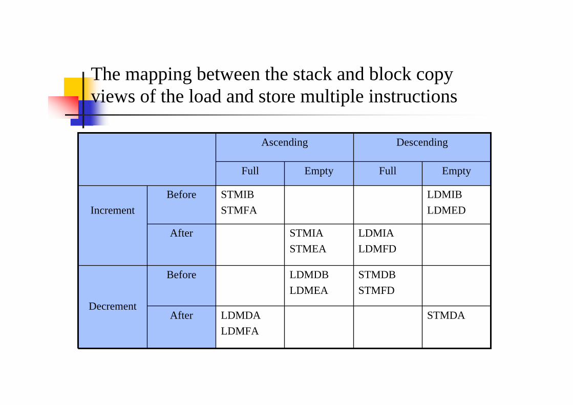
The mapping between the stack and block copy views of the load and store multiple instructions
Decrement
Increment
DescendingAscending
STMDALDMDALDMFA
After
STMDBSTMFD
LDMDBLDMEA
Before
LDMIALDMFD
STMIASTMEA
After
LDMIBLDMED
STMIBSTMFA
Before
EmptyFullEmptyFull

Directives
Data structure definitions and allocation of space for data
Partitioning of files into logical subdivisions
Error reporting and control of assembly listing
Definition of symbols
Conditional and repetitive assembly, and inclusion of subsidiary files.
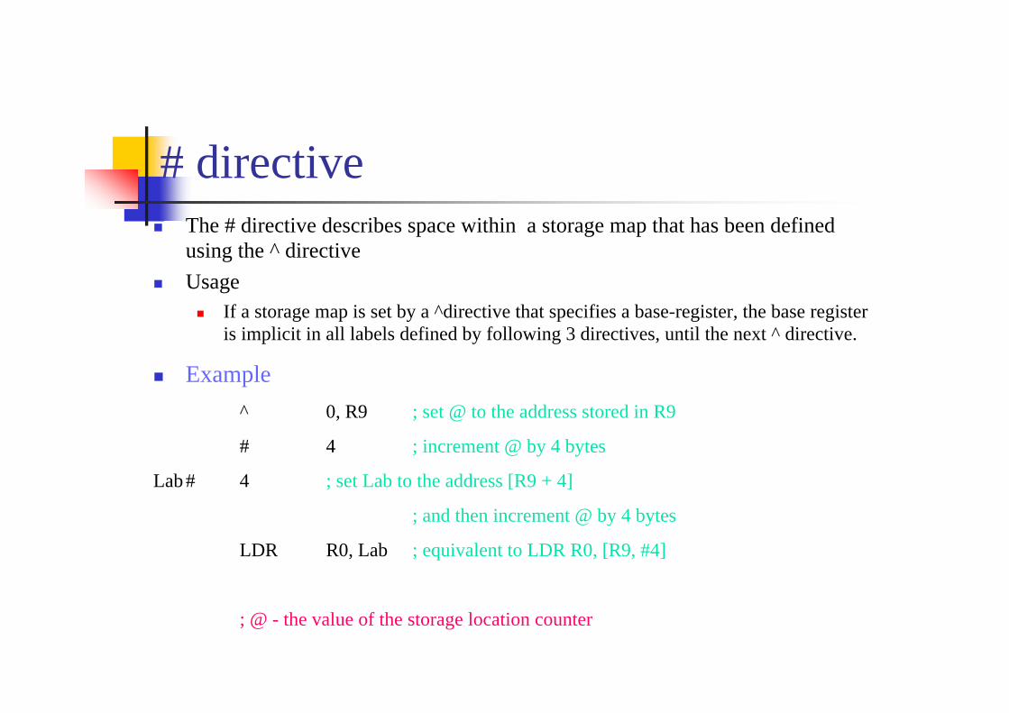
# directiveThe # directive describes space within a storage map that has been defined using the ^ directiveUsage
If a storage map is set by a ^directive that specifies a base-register, the base register is implicit in all labels defined by following 3 directives, until the next ^ directive.
Example^ 0, R9 ; set @ to the address stored in R9
# 4 ; increment @ by 4 bytes
Lab # 4 ; set Lab to the address [R9 + 4]
; and then increment @ by 4 bytes
LDR R0, Lab ; equivalent to LDR R0, [R9, #4]
; @ - the value of the storage location counter

% directiveThe % directive reserves a zeroed block of memory.
ExampleAREA MyData, DATA, READWRITE
Data1 % 255 ; defines 255 bytes of zeroed store

[ or IF directiveThe IF directive introduces a condition that is used to decide whether to assemble a sequence of instructions and/or directivesUsage
Use IF with ENDIF, and optionally with ELSE, for sequences of instructions and/or directives that are only to be assembled or acted on under a specified condition
Example[ Version = “1.0” ; IF …
; code and / or
; directives
| ; ELSE …
; code and / or
; directives
] ; ENDIF

ALIGN directiveBy default, the ALIGN directive aligns the current location within the code to a word(4-byte) boundaryUsage
Use ALIGN to ensure that your code is correctly aligned
ExampleAREA Example, CODE, READONLY
start LDR R6, =label1DCB 1 ; pc misaligned ALIGN ; ensures that lable1 addresses the following
; instructionlabel1 MOV R5, #0x5
AREA cacheable, CODE, ALIGN=4rout1 ; code ; aligned on 16-byte boundary
; codeMOV pc, lr ; aligned only on 4-byte boundaryALIGN 16 ; now aligned on 16-byte boundary
rout2 ; code

Data directiveThe DATA directive informs the assembler that a label is a data-in-code label. This means that the label is the address of data within a code segment.Usage
You must use the DATA directive when you define data in a Thumb code area with any of the data-defining directives such as DCD, DCB, and DCW
ExampleAREA example, CODE
Thumb_fn ; code
; code
MOV pc, lr
Thumb_Data DATA
DCB 1, 3, 4

DCB(=) DCW DCD(&) directivesDirectives allocates one or more bytes( halfword, word ) of memoryUsage
You must use the DATA directive if you use DCB(DCW, DCW) to define labeled data within Thumb code.
ExampleC_string DCB “C_string”, 0
AREA MiscData, DATA, READWRITE
Data DCW -225, 2*number
DCW number + 4
data1 DCD 1, 5, 20 ; Defines 3 words containing decimal values 1, 5, and 20
data2 DCD mem06 ; Defines 1 word containing the address of the label ; mem06
data3 DCD glb + 4 ; Defines 1 word containing 4 + the value of glb
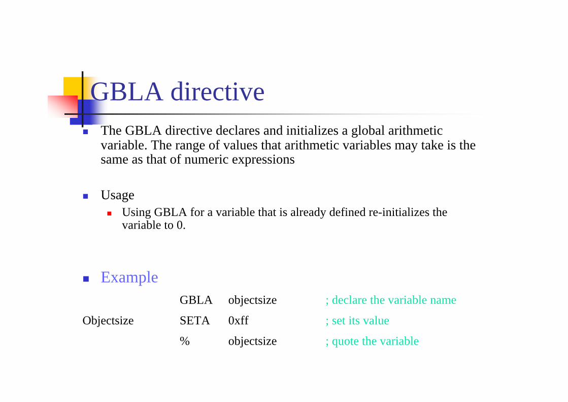
GBLA directiveThe GBLA directive declares and initializes a global arithmetic variable. The range of values that arithmetic variables may take is the same as that of numeric expressions
UsageUsing GBLA for a variable that is already defined re-initializes the variable to 0.
ExampleGBLA objectsize ; declare the variable name
Objectsize SETA 0xff ; set its value
% objectsize ; quote the variable

GET or INCLUDE directiveThe GET directive includes a file within the file being assembled. The included file is assembled. INCLUDE is a synonym for GET
UsageGET is useful for including macro definitions, EQUs, and storage maps in an assembly
ExampleAREA Example, CODE, READONLY
GET file1.s ; include file1 if it exists
; in the current place
GET c:\project\file2.s ; includes files

Instruction Example(1)AREA HelloW, Code, READONLY
SWI_WriteC EQU &0SWI_Exit EQU &11
ENTRYSTART ADR R1, TEXTLOOP LDRB R0, [R1], #1
CMP R0, #0SWINE SWI_WriteCBNE LOOPSWI SWI_Exit
TEXT = “Hello World”, &0a, &0d, 0
END
; declare code area; output character in R0; finish program; code entry point; R1 -> “Hello World”; get the next byte; check for text end; if not end print …; … end loop back; end of execution
; end of program source

Instruction Example(2)AREA Blkcpy, Code, READONLY
SWI_WriteC EQU &0SWI_Exit EQU &11
ENTRYADR R1, TABLE1ADR R2, TABLE2ADR R3, T1END
LOOP1 LDR R0, [R1], #4STR R0, [R2], #4CMP R1, R3BLT R1, R3ADR R1, TABLE2
LOOP2 LDRB R0, [R1], #1CMP R0, #0SWINE SWI_WriteCBNE LOOP2SWI SWI_Exit
TABLE1 = “This is the right string!”, &0a, &0d, 0T1END
ALIGNTABLE2 = “This is the wrong string!”, 0
END
; output character in R0 ; finish program; code entry point; R0 -> TABLE1; R1 -> TABLE2; R3 -> T1END; get TABLE1 1st word; copy into TABLE2; finished?; if not, do more; R1 -> TABLE2; get next byte; check for text end; if not end, print …; … and loop back; finish
;ensure word alignment

Instruction Example(3)AREA Hex_Out, CODE, READONLY
SWI_WriteC EQU &0SWI_Exit EQU &11
ENTRYLDR R1, VALUEBL HexOutSWI SWI_Exit
VALUE DCD &12345678HexOut MOV R2, #8LOOP MOV R0, R1, LSR #28
CMP R0, #9ADDGT R0, R0, #”A”-10ADDLE R0, R0, #”0”SWI SWI_WriteCMOV R1, R1, LSL #4SUBS R2, R2, #1BNE LOOPMOV pc, R14END
; output character in R0; finish program; code entry point; get value to print; call hexadecimal output; finish; test value; nibble count = 8; get top nibble; 0-9 or A-F ?; ASCII alphabetic; ASCII numeric; print character; shift left one nibble; decrement nibble count; if more do next nibble; return

Instruction Example(4)AREA Text_Out, CODE, READONLY
SWI_WriteC EQU &0SWI_Exit EQU &11
ENTRYBL TextOut= “Test string”, &0a, &0d, 0ENTRYBL TextOut= “Test string”, &0a, &0d, 0ALIGNSWI SWI_Exit
TextOut LDRB R0, [R14], #1CMP R0, #0SWINE SWI_WriteCBNE TextOutADD R14, R14, #3BIC R14, R14, #3MOV pc, r14END
; output character in R0; finish program; code entry point; print following string
; finish; get next character; test for end mark; if not end, print …; … and loop; pass next word boundary; round back to boundary; return

Instruction Example(5)#include <stdio.h>
void my_strcpy(char *src, char *dst){
int ch;__asm{loop:LDRB ch, [src], #1STRB ch, [dst], #1CMP ch, #0BNE loop}
}
int main(void){
char a[]= "hello world!";char b[20];__asm{MOV R0, aMOV R1, b BL my_strcpy, {R0, R1}, {}, {}}printf(“Original string = %s\n”, a);printf(“Copied string = s\n”, b);return 0;
}