ab28 multivibrators (astable and monostable) - up org/ab28... · ab28 multivibrators (astable and...
TRANSCRIPT

AB28 Multivibrators (Astable and Monostable)
Operating Manual Ver.1.1
An ISO 9001 : 2000 company
94-101, Electronic Complex Pardesipura, Indore- 452010, India Tel : 91-731- 2570301/02, 4211100 Fax: 91- 731- 2555643 e mail : [email protected] Website : www.scientech.bz Toll free : 1800-103-5050

AB28
Scientech Technologies Pvt. Ltd. 2

AB28
Scientech Technologies Pvt. Ltd. 3
RoHS Compliance
Scientech Products are RoHS Complied. RoHS Directive concerns with the restrictive use of Hazardous substances (Pb, Cd, Cr, Hg, Br compounds) in electric and electronic equipments. Scientech products are “Lead Free” and “Environment Friendly”. It is mandatory that service engineers use lead free solder wire and use the soldering irons upto (25 W) that reach a temperature of 450°C at the tip as the melting temperature of the unleaded solder is higher than the leaded solder.
AB28 Multivibrators
(Astable and Monostable) Table of Contents
1. Introduction 4
2. Theory 6 3. Experiments
• Experiment 1 13 Study of the IC 555 as Monostable (one shot) Multivibrator
• Experiment 2 15 Study of the IC 555 as an Astable (Free running) Multivibrator
4. Data Sheet 17
5. Warranty 18
6. List of Accessories 18

AB28
Scientech Technologies Pvt. Ltd. 4
Introduction AB28 is a compact, ready to use Multivibrator experimental Board. This is useful for students to understand Multivibrator in Astable and Monostable mode using IC NE 555. It can be used as stand alone unit with external DC power supply or can be used with Scientech Analog Lab ST2612 which has built in DC power supply, AC power supply, function generator, modulation generator, continuity tester, toggle switches, and potentiometer.
List of Boards : Model Name AB01 Diode characteristics (Si, Zener, LED) AB02 Transistor characteristics (CB NPN) AB03 Transistor characteristics (CB PNP) AB04 Transistor characteristics (CE NPN) AB05 Transistor characteristics (CE PNP) AB06 Transistor characteristics (CC NPN) AB07 Transistor characteristics (CC PNP) AB08 FET characteristics AB09 Rectifier Circuits AB10 Wheatstone bridge AB11 Maxwell’s Bridge AB12 De Sauty’s Bridge AB13 Schering Bridge AB14 Darlington Pair AB15 Common Emitter Amplifier AB16 Common Collector Amplifier AB17 Common Base Amplifier AB18 RC-Coupled Amplifier AB19 Cascode Amplifier AB20 Direct Coupled Amplifier AB21 Class A Amplifier AB22 Class B Amplifier (push pull emitter follower) AB23 Class C Tuned Amplifier AB24 Transformer Coupled Amplifier AB25 Phase Locked Loop (FM Demodulator & Frequency Divider / Multiplier) AB26 FET Amplifier AB27 Voltage Controlled Oscillator AB29 F-V and V-F Converter AB30 V-I and I-V Converter AB31 Zener Voltage Regulator AB32 Transistor Series Voltage Regulator AB33 Transistor Shunt Voltage Regulator AB35 DC Ammeter AB37 DC Ammeter (0-2mA) AB39 Instrumentation Amplifier

AB28
Scientech Technologies Pvt. Ltd. 5
AB41 Differential Amplifier (Transistorized) AB42 Operational Amplifier (Inverting / Non-inverting / Differentiator) AB43 Operational Amplifier (Adder/Scalar) AB44 Operational Amplifier (Integrator/ Differentiator) AB45 Schmitt Trigger and Comparator AB49 K Derived Filter AB51 Active filters (Low Pass and High Pass) AB52 Active Band Pass Filter AB54 Tschebyscheff Filter AB56 Fiber Optic Analog Link AB57 Owen’s Bridge AB58 Anderson’s Bridge AB59 Maxwell’s Inductance Bridge AB64 RC – Coupled Amplifier with Feedback AB66 Wien Bridge Oscillators AB67 Colpitt Oscillator AB68 Hartley Oscillator AB80 RLC Series and RLC Parallel Resonance AB82 Thevenin’s and Maximum Power Transfer Theorem AB83 Reciprocity and Superposition Theorem AB84 Tellegen’s Theorem AB85 Norton’s theorem AB88 Diode Clipper AB89 Diode Clampers AB90 Two port network parameter AB91 Optical Transducer (Photovoltaic cell) AB92 Optical Transducer (Photoconductive cell/LDR) AB93 Optical Transducer (Phototransistor) AB96 Temperature Transducer (RTD & IC335) AB97 Temperature Transducer (Thermocouple) AB101 DSB Modulator and Demodulator AB102 SSB Modulator and Demodulator AB106 FM Modulator and Demodulator
and many more…………

AB28
Scientech Technologies Pvt. Ltd. 6
Theory The device 555 is a monolithic timing circuit that can produce accurate and highly stable time delays or oscillations. The 555 timer is reliable, easy to use, and economical. IC 555 has been used in number of applications, such as monostable and astable multivibrators, DC-DC converters, digital logic probes, waveform generators, analog frequency meters and tachometers, temperature measurement and control, infrared transmitters, burglar and toxic gas alarms, voltage regulators, etc. The timer 555 is available as an 8-pin metal can, an 8-pin mini DIP, or a 14-pin DIP. Figure 1 shows the functional diagram and the pin configuration of the NE 555 timer. The NE 555 operates over a temperature range of 0° to 70°C. The important features of the NE 555 timer are as follows:
Functional Diagram
Figure 1 • Operation on + 5 to + 18 V supply voltage in both astable and monostable
modes. • Adjustable duty cycle. • Timing from µ sec to hours. • High current output. • Capacity to source or sink current 'of 200 mA. • Output can drive TIL. • Temperature stability of 50 parts per million (ppm) per °C change in
temperature or 0.005% per °C. - Reliable, easy to use, and low cost.
AB28
Scientech Technologies Pvt. Ltd. 7
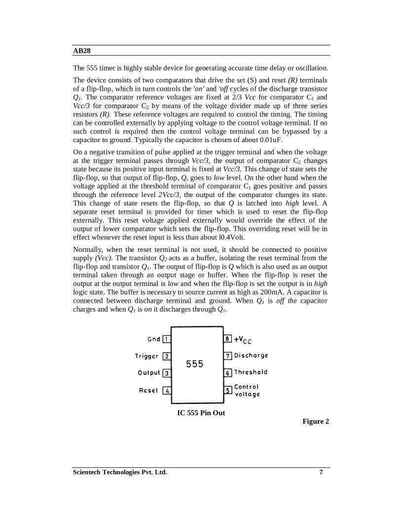
The 555 timer is highly stable device for generating accurate time delay or oscillation. The device consists of two comparators that drive the set (S) and reset (R) terminals of a flip-flop, which in turn controls the 'on' and 'off cycles of the discharge transistor Q1. The comparator reference voltages are fixed at 2/3 Vcc for comparator C1 and Vcc/3 for comparator C2 by means of the voltage divider made up of three series resistors (R). These reference voltages are required to control the timing. The timing can be controlled externally by applying voltage to the control voltage terminal. If no such control is required then the control voltage terminal can be bypassed by a capacitor to ground. Typically the capacitor is chosen of about 0.01uF. On a negative transition of pulse applied at the trigger terminal and when the voltage at the trigger terminal passes through Vcc/3, the output of comparator C2 changes state because its positive input terminal is fixed at Vcc/3. This change of state sets the flip-flop, so that output of flip-flop, Q, goes to low level. On the other hand when the voltage applied at the threshold terminal of comparator C1 goes positive and passes through the reference level 2Vcc/3, the output of the comparator changes its state. This change of state resets the flip-flop, so that Q is latched into high level. A separate reset terminal is provided for timer which is used to reset the flip-flop externally. This reset voltage applied externally would override the effect of the output of lower comparator which sets the flip-flop. This overriding reset will be in effect whenever the reset input is less than about l0.4Volt.
Normally, when the reset terminal is not used, it should be connected to positive supply (Vcc). The transistor Q2 acts as a buffer, isolating the reset terminal from the flip-flop and transistor Q1. The output of flip-flop is Q which is also used as an output terminal taken through an output stage or buffer. When the flip-flop is reset the output at the output terminal is low and when the flip-flop is set the output is in high logic state. The buffer is necessary to source current as high as 200mA. A capacitor is connected between discharge terminal and ground. When Q1 is off the capacitor charges and when Q1 is on it discharges through Q1.
IC 555 Pin Out
Figure 2

AB28
Scientech Technologies Pvt. Ltd. 8
Pin 1 (Ground) : The ground (or common) pin is the most-negative supply potential of the device, which is normally connected to circuit common (ground) when operated from positive supply voltages. Pin 2 (Trigger) : The output of the timer depends on the amplitude of the external trigger pulse applied to this pin. The output is low if the voltage at this pin is greater than 2/3 VCC. However, when a negative going pulse of amplitude larger than 1/3 VCC is applied to this pin, the comparator 2 output goes low, which in turn switches the output to the timer high. The output remains high as long as the trigger terminal is held at a low voltage. Pin 3 (Output) : There are two ways a load can be connected to the output terminal - either between pin 3 and ground (pin 1) called as normally off load or between pin 3 and supply voltage + VCC (pin 8) called as normally on load.
Pin 4 (Reset) : This pin is also used to reset the latch and return the output to a low state. The reset pin will force the output to go low no matter what state the other inputs to the flip-flop are in. When not used, it is recommended that the reset input be tied to V+ to avoid any possibility of false resetting.
Pin 5 (Control Voltage) : An external voltage applied to this terminal changes the threshold as well as the trigger voltage. In other words, by imposing a voltage on this pin or connecting a pot between this pin and ground, the pulse width of the output waveform can be varied. When not used, the control pin should be bypassed to ground with a 0.01µF capacitor to prevent any noise problems. Pin 6 (Threshold) : This is the non-inverting input terminal of the comparator 1, which monitors the voltage across the external capacitor. When the voltage at this pin is greater or equal to the threshold voltage 2/3 VCC, the output of comparator 1 goes high, which in turn switches the output of the timer low. Pin 7 (Discharge) : This pin is connected internally to the collector of transistor T1, as shown in figure 3. When the output is high, T1 is off and acts as an open circuit to the external capacitor C connected across it. On the other hand, when the output is low, T1 is saturated and acts as a short circuit, shorting out the external capacitor C to ground.
Pin 8 (V+) : The V+ pin (also referred to as VCC) is the positive supply voltage terminal of the 555 timer IC. Supply-voltage operating range for the 555 is +4.5 volts (minimum) to +16 volts (maximum), and it is specified for operation between +5 volts and +15 volts.

AB28
Scientech Technologies Pvt. Ltd. 9
IC 555 as Monostable Multivibrator :
IC 555 as Monostable multivibrator (a) Functional Diagram (b) waveform at
various points (c) External Connections Figure 3

AB28
Scientech Technologies Pvt. Ltd. 10
The resistance R and the capacitor C are external to the chip, and their values determine the output pulse width. Before the application of the trigger pulse vt , the voltage at the trigger input pin is high which is equal to Vcc [say V (1)]. With this high trigger input, the output of comparator C2 will be low [say V(0)], causing the flip-flop output Q to be high, i.e. Q = V (1) and Vo = V (0) = 0 (due to inverter circuit). With Q = V (1), the discharge transistor Q1 will be saturated and the voltage across the timing capacitor C will be essentially zero, i.e. Vx = O. The output Va = 0 V is the quiescent state of the timer device.
At t = 0, application of trigger vt, (negative going pulse shown in [Figure 3(b)] less than Vcc/3 causes the output of comparator C2 to be high, i.e. V (1). This will set the flip-flop with Q now low. i.e, Q = V (0). This makes Vo = V (1). Due to Q = V(0), discharge transistor will be turned 'off’. Note that after termination of the trigger pulse the flip-flop will remain in the Q = V (0) state. Now, the timing capacitor charges up towards Vcc via resistor R, with a time constant t = RC. The charging up expression is
…………..(1) where vx is the voltage across C at any time t. When vx reaches the threshold voltage level of 2Vcc/3, comparator C1 will switch states and its output voltage will now be high. This causes the flip-flop to reset so that Q will go high. i.e. V (1), and Vo returns to original level V (0). The high value of Q turns on the discharge transistor Q1 . The low saturation resistance of Q1 discharges C quickly.
The end of the output pulse occurs at time T1, at which point vx =2 Vcc/3. Thus the pulse width T1 is determined by the time required for the capacitor voltage vx to charge from zero to 2Vcc/3. This period can be obtained by putting vx = 2Vcc/3 at t= T, Thus from eq.1
…………(2) Note that the pulse duration is independent of the supply voltage Vcc. The trigger pulse width must be shorter in duration than T1 for proper operation of the timer. In Eq.2 we have assumed V (0) = 0.
The timing cycle may be interrupted by connecting the reset terminal (pin 4). This turns on transistor Q1 and the capacitor is prevented from charging.

AB28
Scientech Technologies Pvt. Ltd. 11
IC 555 as Astable Multivibrator :
Astable Multivibrator (a) Functional Diagram (b) Waveform at various points
(c) external connection diagram Figure 4
In this mode of operation, the timing capacitor charges up toward Vcc (assuming VO is high initially) through (RA + RB) until the voltage across the capacitor reaches the threshold level of 2 Vcc/3. At this point comparator C1 switches state causing the flip-flop output Q to go high i.e., Q = V (1). This turns on the discharge transistor Q1 and the timing capacitor C then discharges through RB and Q1 (pin 7). The discharging continues until the capacitance voltage drops to Vcc/3, at which point comparator C2 switches states causing the flip-flop output Q to go low, i.e., Q = V(0), turning off the discharge transistor Q1. At this point the capacitor starts to charge again, thus completing the cycle.
The output voltage and capacitor voltage waveforms are shown in Figure 4(b) As shown here, the capacitor is periodically charged and discharged between 2 Vcc/3 and Vcc/3, respectively.

AB28
Scientech Technologies Pvt. Ltd. 12
The charging time is given by, Tc = (RA + RB) C In 2
= 0.693 (RA + RB) C The discharging time is given by,
TD = RB C In 2 = 0.639 RB C
The total period T = TC +TD
T = 0.693 (RA + 2RB) C And the frequency of oscillations will be
1 10.693( 2 )
foT R R CBA
= =+
1.44
( 2 )fo
R R CBA=
+

AB28
Scientech Technologies Pvt. Ltd. 13
Experiment 1 Objective : Study of IC 555 as a mono stable (one shot) Multivibrator Equipments Needed : 1. Analog board of AB28. 2. DC power supplies + 5V, from external source or ST2612 Analog Lab. 3. 2 mm patch cords. 4. Ohm meter.
5. Function generator [for pulse signal (Scientech Function Generator ST4062, ST4063 etc.)]
Circuit diagram : Circuit used to study monostable multivibrator is shown in Figure 5.
Figure 5
AB28
Scientech Technologies Pvt. Ltd. 14
Procedure :
• Connect power supply + 5V from ST2612 or any external source. 1. Connect point a to point b using a 2mm patch cord.
2. Connect point c to point d/e using a 2mm patch cord. 3. Keep the pot (R2 1M) to fully anticlockwise direction.
4. Apply a pulse signal of 5Vpp and 1 KHz (keep duty cycle of pulse 50%) at pin 2 of IC 555 i.e. to the point e/g on AB28 board. Observe the same on oscilloscope CHI.
5. Connect pin 3 of IC55 i.e. output socket to the oscilloscope CHII.
6. Vary the pot and observe the variation of output pulse duty cycle with the change in resistance R (where, R=R1+R2).
7. For any value of R measure the ON time of output pulse. 8. Calculate the same by following equation for theoretically calculating the output
pulse ‘On’ time. TP = 1.1 * R1C1
Note : For calculating the value of R, disconnect the +5V supply and connection between point a and b. Connect ohmmeter between point a and TP1. The ohmmeter will read the value of R.
9. Verify theoretical and practical values of TP.
Note : The two values of TP (theoretical and practical values) will match only for time for which input pulse is High i.e. only for ‘On’ 'time of input pulse. To verify this vary the duty cycle of input signal and check the output pulse duty cycle by varying R (R=R1+R2).
10. Repeat above procedure for different values of R.
AB28
Scientech Technologies Pvt. Ltd. 15
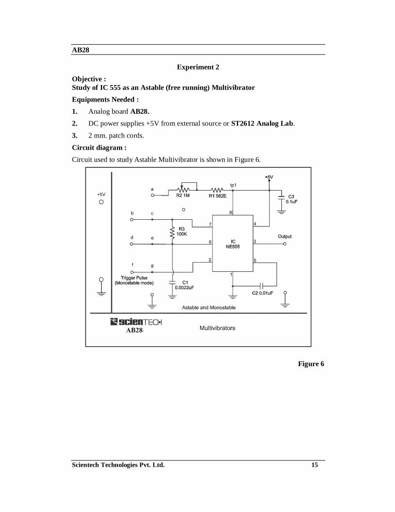
Experiment 2 Objective : Study of IC 555 as an Astable (free running) Multivibrator Equipments Needed : 1. Analog board AB28. 2. DC power supplies +5V from external source or ST2612 Analog Lab. 3. 2 mm. patch cords.
Circuit diagram : Circuit used to study Astable Multivibrator is shown in Figure 6.
Figure 6

AB28
Scientech Technologies Pvt. Ltd. 16
Procedure :
• Connect power supply +5V from ST2612 or any external source. 1. Connect point a to point b using a 2mm patch cord.
2. Connect point d to point f/g using a 2mm patch cord. 3. Keep the pot (R2 1M) to fully anticlockwise direction.
4. Connect pin 3 of IC55 i.e. output socket to the oscilloscope. 5. Vary the pot and observe the variation of output signal’s frequency with the
change in resistance R (where, R=R1+R2). 6. To verify the above calculate the frequency of output signal using following
equation
( )1.44
1 2 3fout
C R R=
+
Note : For calculating the value of R, disconnect the +5V supply and connection between point a and b. Connect ohmmeter between point a and TP1. The ohmmeter will read the value of R.
7. Trace the waveforms of the voltage across capacitor C1 and ground.
8. Repeat above procedure for different values of R.

AB28
Scientech Technologies Pvt. Ltd. 17
Data Sheet

AB28
Scientech Technologies Pvt. Ltd. 18
Warranty 1. We guarantee the product against all manufacturing defects for 24 months from
the date of sale by us or through our dealers. Consumables like dry cell etc. are not covered under warranty.
2. The guarantee will become void, if
a) The product is not operated as per the instruction given in the operating manual.
b) The agreed payment terms and other conditions of sale are not followed.
c) The customer resells the instrument to another party. d) Any attempt is made to service and modify the instrument.
3. The non-working of the product is to be communicated to us immediately giving full details of the complaints and defects noticed specifically mentioning the type, serial number of the product and date of purchase etc.
4. The repair work will be carried out, provided the product is dispatched securely packed and insured. The transportation charges shall be borne by the customer.
For any Technical Problem Please Contact us at [email protected]
List of Accessories
1. 2 mm Patch Cords (Red) ........................................................................1 No. 2. 2 mm Patch Cord (Blue) ....................................................................... 4 Nos. 3. 2 mm Patch Cord (Black) ..................................................................... 3 Nos. 4. e-Manual.................................................................................................1 No.
Updated 25-03-2009