a wideband low-power cascade ∑∆ modulator based … · a wideband low-power cascade ∑∆...
TRANSCRIPT

A Wideband Low-Power Cascade ∑∆ Modulator Based on Considerations of the Integrator Settling Behavior
YI YIN1, HEINRICH KLAR2, PETER WENNEKERS1
(1) TSO-EMEA, RF/IF Innovation Center Munich Freescale Semiconductor
Schatzbogen 7, 81829 Munich, Gemany
(2) Technical University of Berlin -Institute of Computer Engineering and Microelectronics , Berlin Germany
Abstract: - This paper presents a study of the effect of settling error due to finite gain-bandwidth product (GBW) and slew-rate (SR) of opamps in SC Σ∆ A/D modulators. Based on the theoretical point of view, a new architecture for cascade multibit Σ∆ A/D modulators is proposed to achieve better performances at low oversampling ratio. The performance improvement is analyzed and compared with traditional cascade architectures. Simulation results show that the proposed Sigma-Delta modulator relaxes the circuit requirement on the GBW of opamps up to twice the sampling frequency. At the same time, the requirement on slew rate is significantly low, so that it can be automatically satisfied for an adequate settle during its settling phase. Therefore, the proposed architecture is suitable for wideband and low-power applications. Moreover, it is shown that the proposed architecture is also immune to other non-idealities, such as finite DC-gain, capacitor mismatching and non-linear DC-gain. Key-Words: - Analog integrated circuits, high-speed high-resolution analog–to-digital converters, and sigma–delta modulator 1 Introduction High-speed high-resolution analog-to-digital converters (ADCs) are one of the key devices in measurement equipment and communication systems. Therefore, many different ADCs based on various kinds of ADC topologies have been developed. Among them, Sigma-Delta ADCs have been frequently applied to realize high resolution under the consideration of low cost and power consumption. For high-speed applications, integrator defective settling is the main bottleneck in the present wideband SC Sigma-Delta modulator designs. Many low oversampling high-resolution modulators use MASH structures [2]–[4], where 1-bit quantizer is commonly used in the first stage, to avoid the performance degradation due to the non-linearity of DAC. However, these structures need a high opamp GBW to relieve the impact on the settling error. With the development of the efficient dynamic element matching (DEM) techniques [6]-[8], multibit quantization has been recently used in SC single-loop Sigma-Delta modulators to realize high-resolution at low OSR. Although, the required opamp GBW can be relaxed by using multibit quantizers, it is practically difficult to be obtained, since high-order single-loop modulators are formed by cascading multiple integrators in the forward path, and therefore, the dc gain of the forward path is very high. As a result, the signal, which is sensed by quantizer,
is almost independent of the input signal. Therefore the input levels of integrators are still high [8]. Another problem associated with settling error of all of the aforementioned structures is the appearance of harmonic distortion due to the gain dependence of the integrator on its input, when opamp dynamic operation is in partial slewing. In this paper, the effect of settling error thermal noise on the performance of SC Sigma-Delta modulators will be discussed, and an efficient interdependency between finite GBW and SR of opamps will be described for estimating the minimum demand on the GBW of opamps. Following it, a new cascade Sigma-Delta modulator architecture is presented, which combines the merits of cascaded Sigma-Delta Modulator structure, low distortion structure [9], and multibit quantization. This ADC development relaxes the GBW of opamps as low as twice the sampling frequency fS, much lower than that in other Sigma-Delta modulator implementations [3]-[5]. Another advantage of the proposed modulator is that it is insensitive to circuit non-idealities. Section 2 contains a general analysis of the settling behavior in the SC integrators. Section 3 describes the newly-proposed architecture. Section 4 presents the simulation results for the validation of performance improvements. The conclusion is followed in Sections 5.
Proceedings of the 5th WSEAS Int. Conf. on Instrumentation, Measurement, Circuits and Systems, Hangzhou, China, April 16-18, 2006 (pp112-116)

2 Analysis of Settling Behavior 2.1 SC integrator simplified model The settling error is caused by GBW and SR of amplifiers in SC Sigma-Delta modulators [1] [2]. The simplified model of a SC integrator is shown in Fig.1, which consists of two pairs of input samplers, a sampling capacitor CS, an integration capacitor CI and a single-pole amplifier. The amplifier is modeled by the transconductance gm, with biasing current IBIAS , CGS and CL standing for a parasitic capacitor associated with the summation node of the amplifier input and a capacitive load, which includes parasitics at the amplifier’s output node and the parasitic associated with the bottom plate of the integration capacitor CI, respectively.
Fig. 1 Simplified CMOS integrator schematic
In this case, the equivalent closed-loop capacitance at the integrator output depends on the equivalent open-loop capacitance (Ccl,ol) and the dc feedback factor (f) during the integration phase, and it is given by [11]:
I
LIGSSGSS
oleqcleq C
CCCCCC
fC
C)(,
,++
++==
(1) Therefore, the close-loop time constant and slew rate are obtained, respectively [2]:
m
cleq
gC ,=τ (2)
cleq
BIAS
CI
SR,
= (3)
Furthermore, the relationship between the slew rate and the time constant has been derived using the simple square-law model of the MOS transistors [2]:
22* effthGS
m
BIAS VVVg
ISR =
−==τ (4)
Where VGS is the quiescent gate-to-source voltage of the input transistor, Vth is its threshold voltage, and Veff is the overdrive voltage. Reforming (4) by introducing
gain-bandwidth product GBW, a more design-oriented constant is obtained:
effVGBW
SR π= (5)
It indicates that both design parameters SR and GBW are directly proportional to IBIAS, and therefore, the ratio is quite constant in opamps, which depends directly on the overdrive voltage. 2.2 Settling Behavior of the SC integrator With respect to the settling error, two separate cases have been considered [5]:
1. In the case of
τ
s
I
S vCC
SR ≥ (7)
there is no slew-rate limitation, and the integrator output will be linearly settled.
2. In the case of
τs
I
S vCC
SR < (8)
and
s
s
I
S
fSRv
CC
t21
0 <−= τ (9)
the op-amp is first in slewing within t0, and therefore, the integrator output shows a partially SR limited nonlinear settling. Imposing (4) in (7) and reforming, we get the linearly-settling condition:
sI
Seff v
CC
V 2≥ (10)
Similarly, imposing (4) in (8) and (9), the partially SR limited nonlinear settling condition with GBnorm=GBW/fs is:
vSI
Seff
norm
s
I
S
CC
VGBv
CC
21
2 <<+π
(11)
The linear settling error can be approximated as:
( )normS
st GBT πτ
ε −=⎟⎠⎞
⎜⎝⎛−≅ exp
2exp (12)
whereas the nonlinear settling error can be approximately evaluated as:
⎟⎟⎠
⎞⎜⎜⎝
⎛+−−≅
τττε
SRv
CC
Tv
CCSR s
I
SS
SI
Sst 12exp**
⎟⎟
⎠
⎞
⎜⎜
⎝
⎛+−−=
⎟⎟⎠
⎞⎜⎜⎝
⎛+−−≅
eff
notmnorm
norm
eff
eff
s
I
S
Ss
I
S
eff
VGB
V
Vv
CC
fGBW
vCCV
vv
21exp*2
21exp*2
π
π
(13)
Proceedings of the 5th WSEAS Int. Conf. on Instrumentation, Measurement, Circuits and Systems, Hangzhou, China, April 16-18, 2006 (pp112-116)

Fig. 2 The relationship between the demanded normalized GB and the relative integrator input level
for a given settling error Fig. 2 illustrates the corresponding relationship between the normalized GB and the integrator’s relative input level. The output response of the integrator is assumed to be settled to a given error of 0.05%, 0.1% and 0.5%, respectively, and Veff=200mV. It is shown that the low input level of the integrator is the key to reduce the required normalized gain-bandwidth GB. Note that most of the other existing Sigma-Delta modulators have a great occurrence that the input levels of the integrators are relatively large, so that eq. (10) is not satisfied. Therefore, they operate mostly in the non-linear settling region. Consequently, a relatively large opamp gain-bandwidth is required, and harmonics is produced. Additionally, the opamp normalized gain-bandwidth GB can also be reduced by using a certain topology, which is insensitive to the settling error. 3 Proposed Σ∆ Modulator With respect to saving power and maximizing the conversion rate, the most essential issue in the design of ADC’s is to reduce the normalized GB as much as possible, whereas the resolution of the converter is not deteriorated. It means, when the signal bandwidth is fixed, fs is also fixed, and the reduced requirement on the opamp GBW results in a smaller IBIAS, and thus smaller power consumption; on the other hand, when the opamp GBW is fixed due to technology limitation, a higher fs can be used, resulting in extended signal bandwidth. Based on the analysis on the settling behavior of SC integrators, a new alternative approach to realize wideband and wide-dynamic-range ADC is proposed, in which the low-distortion multi-bit Sigma-Delta modulator concept [9] is introduced into cascaded sigma delta modulators. The proposed generic architecture is shown in Fig.3, where gN1, gN2, gN3 are the interstage
scaling factors in the nth stage. With the consideration of physically achievable output swings, in combination of behavior simulation and statistical optimization, we obtain;
gi1=1 gi2=1 gi1=0.5 i=2….N-1 gN1=1 gN2=0.5 gN3=1
H(z) in the blocks denotes the integration function:
( ) 1
1
1 −
−
−=
zzzH (14)
Fig. 3. The proposed N-stage cascade Sigma-Delta
modulator Ideally, the quantization error in all stages except the last one of the cascade structure can be completely cancelled in the digital domain. Therefore, the output signal can be expressed as the combination of the delayed input signal and the (N+1)th-order noise-shaped quantization noise (N is the number of cascaded stages), that is:
( ) 111 )1(* +−−− −+= NN
N zEzXY (15) where EN indicates the last-stage quantization error. Note that the proposed interstage scaling factors do not degrade the dynamic range as other cascade structures. The key advantage over other high-order cascades is that the individual input level of the integrators is considerably lower, even with high feedforward gain CS/CI=1 in the two integrators of first stage, as only low-level quantization noise E is introduced in the integrator loops. To illustrate this, Fig. 4 shows the histogram of the integrator inputs (X1 and X2) and quantizer input (X3) for an input signal with amplitude of -3 dBFS. Fig.5 presents the performance improvement with respect to the settling error by comparing the SNDR, signal-to-(noise+distortion) ratio, vs. the normalized GB
Proceedings of the 5th WSEAS Int. Conf. on Instrumentation, Measurement, Circuits and Systems, Hangzhou, China, April 16-18, 2006 (pp112-116)
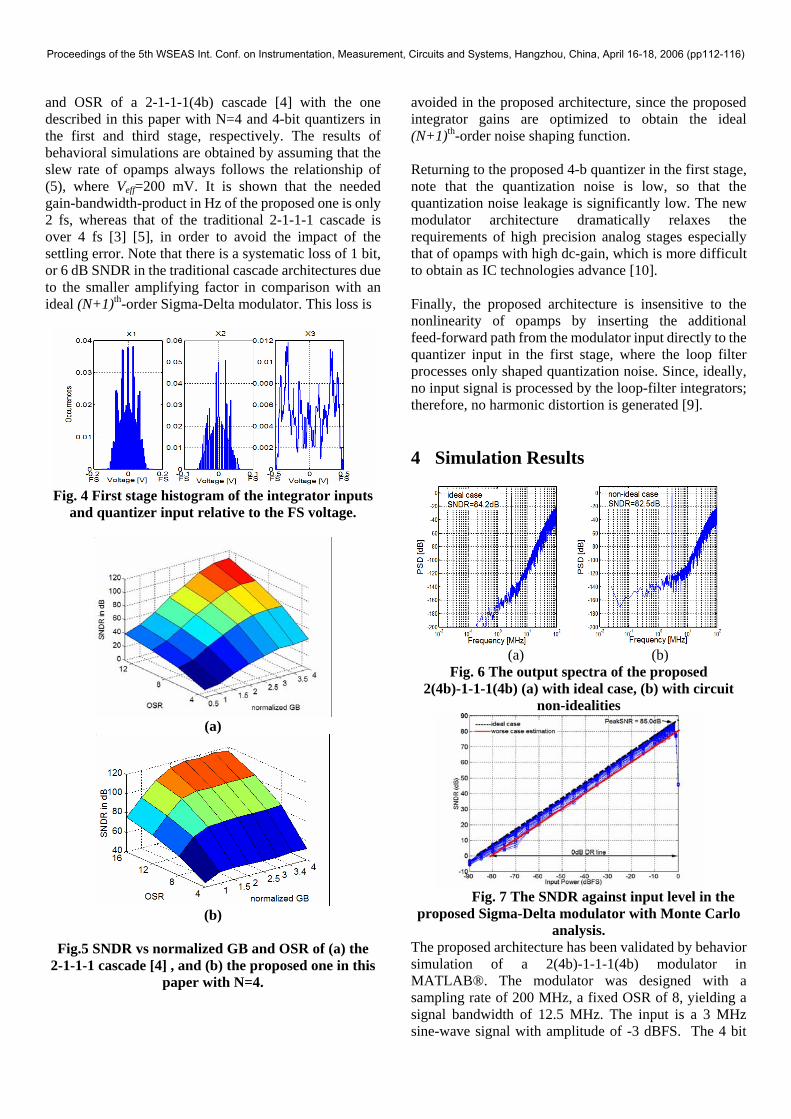
and OSR of a 2-1-1-1(4b) cascade [4] with the one described in this paper with N=4 and 4-bit quantizers in the first and third stage, respectively. The results of behavioral simulations are obtained by assuming that the slew rate of opamps always follows the relationship of (5), where Veff=200 mV. It is shown that the needed gain-bandwidth-product in Hz of the proposed one is only 2 fs, whereas that of the traditional 2-1-1-1 cascade is over 4 fs [3] [5], in order to avoid the impact of the settling error. Note that there is a systematic loss of 1 bit, or 6 dB SNDR in the traditional cascade architectures due to the smaller amplifying factor in comparison with an ideal (N+1)th-order Sigma-Delta modulator. This loss is
Fig. 4 First stage histogram of the integrator inputs
and quantizer input relative to the FS voltage.
(a)
(b)
Fig.5 SNDR vs normalized GB and OSR of (a) the
2-1-1-1 cascade [4] , and (b) the proposed one in this paper with N=4.
avoided in the proposed architecture, since the proposed integrator gains are optimized to obtain the ideal (N+1)th-order noise shaping function. Returning to the proposed 4-b quantizer in the first stage, note that the quantization noise is low, so that the quantization noise leakage is significantly low. The new modulator architecture dramatically relaxes the requirements of high precision analog stages especially that of opamps with high dc-gain, which is more difficult to obtain as IC technologies advance [10]. Finally, the proposed architecture is insensitive to the nonlinearity of opamps by inserting the additional feed-forward path from the modulator input directly to the quantizer input in the first stage, where the loop filter processes only shaped quantization noise. Since, ideally, no input signal is processed by the loop-filter integrators; therefore, no harmonic distortion is generated [9]. 4 Simulation Results
(a) (b)
Fig. 6 The output spectra of the proposed 2(4b)-1-1-1(4b) (a) with ideal case, (b) with circuit
non-idealities
Fig. 7 The SNDR against input level in the
proposed Sigma-Delta modulator with Monte Carlo analysis.
The proposed architecture has been validated by behavior simulation of a 2(4b)-1-1-1(4b) modulator in MATLAB®. The modulator was designed with a sampling rate of 200 MHz, a fixed OSR of 8, yielding a signal bandwidth of 12.5 MHz. The input is a 3 MHz sine-wave signal with amplitude of -3 dBFS. The 4 bit
Proceedings of the 5th WSEAS Int. Conf. on Instrumentation, Measurement, Circuits and Systems, Hangzhou, China, April 16-18, 2006 (pp112-116)
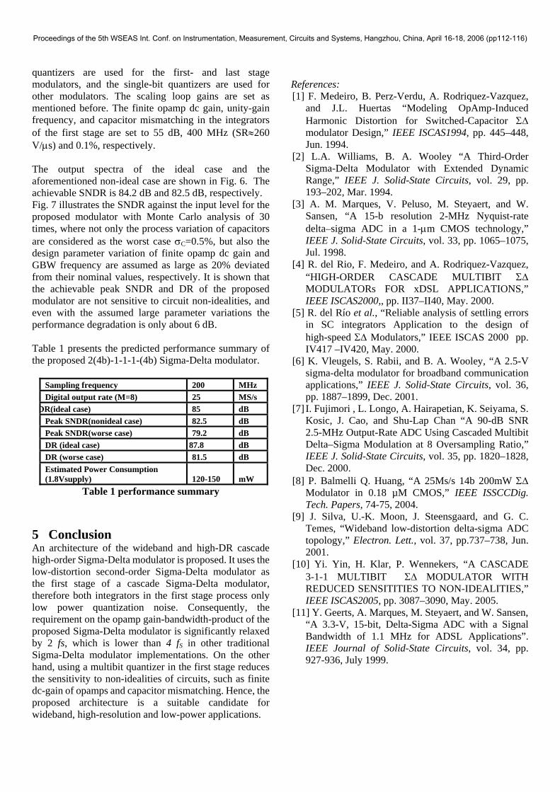
quantizers are used for the first- and last stage modulators, and the single-bit quantizers are used for other modulators. The scaling loop gains are set as mentioned before. The finite opamp dc gain, unity-gain frequency, and capacitor mismatching in the integrators of the first stage are set to 55 dB, 400 MHz (SR≈260 V/µs) and 0.1%, respectively. The output spectra of the ideal case and the aforementioned non-ideal case are shown in Fig. 6. The achievable SNDR is 84.2 dB and 82.5 dB, respectively. Fig. 7 illustrates the SNDR against the input level for the proposed modulator with Monte Carlo analysis of 30 times, where not only the process variation of capacitors are considered as the worst case σC=0.5%, but also the design parameter variation of finite opamp dc gain and GBW frequency are assumed as large as 20% deviated from their nominal values, respectively. It is shown that the achievable peak SNDR and DR of the proposed modulator are not sensitive to circuit non-idealities, and even with the assumed large parameter variations the performance degradation is only about 6 dB.
Table 1 presents the predicted performance summary of the proposed 2(4b)-1-1-1-(4b) Sigma-Delta modulator.
Sampling frequency 200 MHz Digital output rate (M=8) 25 MS/s
DR(ideal case) 85 dB Peak SNDR(nonideal case) 82.5 dB Peak SNDR(worse case) 79.2 dB DR (ideal case) 87.8 dB DR (worse case) 81.5 dB Estimated Power Consumption (1.8Vsupply) 120-150 mW
Table 1 performance summary
5 Conclusion An architecture of the wideband and high-DR cascade high-order Sigma-Delta modulator is proposed. It uses the low-distortion second-order Sigma-Delta modulator as the first stage of a cascade Sigma-Delta modulator, therefore both integrators in the first stage process only low power quantization noise. Consequently, the requirement on the opamp gain-bandwidth-product of the proposed Sigma-Delta modulator is significantly relaxed by 2 fs, which is lower than 4 fS in other traditional Sigma-Delta modulator implementations. On the other hand, using a multibit quantizer in the first stage reduces the sensitivity to non-idealities of circuits, such as finite dc-gain of opamps and capacitor mismatching. Hence, the proposed architecture is a suitable candidate for wideband, high-resolution and low-power applications.
References: [1] F. Medeiro, B. Perz-Verdu, A. Rodriquez-Vazquez,
and J.L. Huertas “Modeling OpAmp-Induced Harmonic Distortion for Switched-Capacitor Σ∆ modulator Design,” IEEE ISCAS1994, pp. 445–448, Jun. 1994.
[2] L.A. Williams, B. A. Wooley “A Third-Order Sigma-Delta Modulator with Extended Dynamic Range,” IEEE J. Solid-State Circuits, vol. 29, pp. 193–202, Mar. 1994.
[3] A. M. Marques, V. Peluso, M. Steyaert, and W. Sansen, “A 15-b resolution 2-MHz Nyquist-rate delta–sigma ADC in a 1-µm CMOS technology,” IEEE J. Solid-State Circuits, vol. 33, pp. 1065–1075, Jul. 1998.
[4] R. del Rio, F. Medeiro, and A. Rodriquez-Vazquez, “HIGH-ORDER CASCADE MULTIBIT Σ∆ MODULATORs FOR xDSL APPLICATIONS,” IEEE ISCAS2000,, pp. II37–II40, May. 2000.
[5] R. del Río et al., “Reliable analysis of settling errors in SC integrators Application to the design of high-speed Σ∆ Modulators,” IEEE ISCAS 2000 pp. IV417 –IV420, May. 2000.
[6] K. Vleugels, S. Rabii, and B. A. Wooley, “A 2.5-V sigma-delta modulator for broadband communication applications,” IEEE J. Solid-State Circuits, vol. 36, pp. 1887–1899, Dec. 2001.
[7] I. Fujimori , L. Longo, A. Hairapetian, K. Seiyama, S. Kosic, J. Cao, and Shu-Lap Chan “A 90-dB SNR 2.5-MHz Output-Rate ADC Using Cascaded Multibit Delta–Sigma Modulation at 8 Oversampling Ratio,” IEEE J. Solid-State Circuits, vol. 35, pp. 1820–1828, Dec. 2000.
[8] P. Balmelli Q. Huang, “A 25Ms/s 14b 200mW Σ∆ Modulator in 0.18 µM CMOS,” IEEE ISSCCDig. Tech. Papers, 74-75, 2004.
[9] J. Silva, U.-K. Moon, J. Steensgaard, and G. C. Temes, “Wideband low-distortion delta-sigma ADC topology,” Electron. Lett., vol. 37, pp.737–738, Jun. 2001.
[10] Yi. Yin, H. Klar, P. Wennekers, “A CASCADE 3-1-1 MULTIBIT Σ∆ MODULATOR WITH REDUCED SENSITITIES TO NON-IDEALITIES,” IEEE ISCAS2005, pp. 3087–3090, May. 2005.
[11] Y. Geerts, A. Marques, M. Steyaert, and W. Sansen, “A 3.3-V, 15-bit, Delta-Sigma ADC with a Signal Bandwidth of 1.1 MHz for ADSL Applications”. IEEE Journal of Solid-State Circuits, vol. 34, pp. 927-936, July 1999.
Proceedings of the 5th WSEAS Int. Conf. on Instrumentation, Measurement, Circuits and Systems, Hangzhou, China, April 16-18, 2006 (pp112-116)