a three-stage cascaded staggered double vane for a … · a three-stage cascaded staggered double...
TRANSCRIPT

Plasma and Fusion Research: Regular Articles Volume 10, 1406078 (2015)
A Three-Stage Cascaded Staggered Double Vanefor a 220 GHz Traveling-Wave Tube
Guangsheng DENG, Xiaoling HUANG, Jun YANG, Zhiping YIN and Jiufu RUANAcademy of Opto-Electronic Technology, Hefei University of Technology, Hefei, 230009, China
(Received 16 June 2015 / Accepted 12 August 2015)
This paper presents a simulation of a three-stage cascaded staggered double vane slow-wave structure (SWS).The results suggest that >10 W of peak power can be produced between 208 GHz and 238 GHz and a maximumgain of 32.4 dB at 220 GHz, driven by three 20 mA electron beams. The proposed circuit does not require anattenuator and the length of each stage is 27.45 mm. Because of the current density and short circuit length, thestructure shows application potential as a terahertz radiation source.
c© 2015 The Japan Society of Plasma Science and Nuclear Fusion Research
Keywords: multi-beam, cascaded amplifier, staggered double vane (SDV), slow-wave structure (SWS)
DOI: 10.1585/pfr.10.1406078
1. IntroductionBecause of advances in fabrication and device physics
modeling [1, 2], the interest in new, practical sources ofterahertz (THz) vacuum electronic devices (VEDs) has re-cently resurged. The traveling-wave tube (TWT) is oneof the most important terahertz wave vacuum amplifiersbecause of its outstanding bandwidth and power capac-ity. Some 0.22-THz TWTs for the atmospheric windowhave been developed [3, 4], which have also been investi-gated recently [5,6]. Paoloni and Mineo [7] studied a TWTbased on the double corrugated waveguide. Hou et al. [8]proposed a novel slow-wave structure (SWS) called ridge-vane-loaded folded waveguide. Xu et al. [9] and Shin etal. [10] presented a THz TWT based on a sine waveguideand staggered double vane (SDV), respectively. Most ofthe THz TWTs require relatively long circuit lengths; how-ever, fabrication issues, beam interception, and electronbeam thermal effects dominate and ultimately limit thecircuit length in practice. Moreover, the fabrication oftiny concentrated attenuators, necessary for high-gain THzTWTs, is challenging.
Nguyen et al. [11] presented a TWT based on a three-stage cascaded folded waveguide with every stage con-nected end-to-end and the RF carrying information be-tween the stages. In this structure, the circuit length issignificantly reduced. Based on this idea, we propose athree-stage cascaded SDV TWT with the advantages ofthe cascaded folded waveguide TWT. Moreover, in sucha cascaded SDV TWT, only a 20 mA beam current is re-quired at each stage. Compared with the cascaded foldedwaveguide TWT having the same output power, the beamcurrent in our proposed TWT is 20% lower, offering sig-nificant improvements in beam generation and focusing.
author’s e-mail: [email protected]
2. Model and Transmission Charac-teristicsThe 3D single cell of the SDV SWS is shown in
Fig. 1, together with the dispersion curve of the fundamen-tal mode under the first spatial harmonic operation basedon the CST eigenmode calculation. The normalized phasevelocity is given by
vNor = vp/c, (1)
where vp is the phase velocity of the fundamental modeunder the first spatial harmonic, and c is the speed of light.
In the SWS of a TWT, the interaction impedance ofthe first spatial harmonic is given by
kc =|Ez|2
2β2Pw, (2)
Fig. 1 Dispersion curve of the fundamental mode under the firstspatial harmonic of the SWS. The insert shows the single-cell 3D schematic of the SWS with geometric parameters.
c© 2015 The Japan Society of PlasmaScience and Nuclear Fusion Research
1406078-1
Plasma and Fusion Research: Regular Articles Volume 10, 1406078 (2015)
Fig. 2 Average interaction impedance of the SWS. The insertshows the beam cross section and beam tunnel cross sec-tion.
Fig. 3 Three-dimensional model of the three-stage cascadedSDV SWS.
where Pw is the electromagnetic wave power along the ax-ial direction, and Ez and β are the amplitudes of the axialcomponent of the electric field and the phase constant ofthe first spatial harmonic, respectively. The effectivenessof beam–wave interaction depends on the average interac-tion impedance over the cross section of the beam; thus,400 points uniformly distributed on the beam cross sec-tion were used in the calculation, as shown in Fig. 2. Atlower frequencies, the interaction impedance is relativelyhigh, the phase velocity varies drastically, and synchro-nization of the electron beam and electromagnetic wave isdifficult. As frequency increases, the dispersion and inter-action impedance curves flatten; therefore, the beam–waveinteraction stabilizes at high frequencies.
Figure 3 shows the three-stage cascaded SDV SWSmodel. The three-stage structure is adopted to reducethe circuit length in each stage and to increase the out-put power. Each stage is connected by a straight waveg-uide and an input–output coupler that comprises the tran-sition structure of the SWS and an input–output connector.The end of the third stage is at the axial position, where
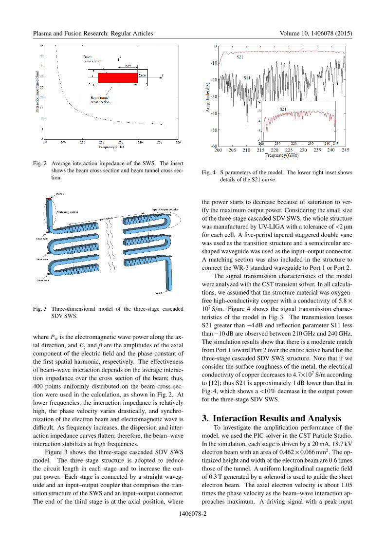
Fig. 4 S parameters of the model. The lower right inset showsdetails of the S21 curve.
the power starts to decrease because of saturation to ver-ify the maximum output power. Considering the small sizeof the three-stage cascaded SDV SWS, the whole structurewas manufactured by UV-LIGA with a tolerance of <2 µmfor each cell. A five-period tapered staggered double vanewas used as the transition structure and a semicircular arc-shaped waveguide was used as the input–output connector.A matching section was also included in the structure toconnect the WR-3 standard waveguide to Port 1 or Port 2.
The signal transmission characteristics of the modelwere analyzed with the CST transient solver. In all calcula-tions, we assumed that the structure material was oxygen-free high-conductivity copper with a conductivity of 5.8 ×10⁷ S/m. Figure 4 shows the signal transmission charac-teristics of the model in Fig. 3. The transmission lossesS21 greater than −4 dB and reflection parameter S11 lessthan −10 dB are observed between 210 GHz and 240 GHz.The simulation results show that there is a moderate matchfrom Port 1 toward Port 2 over the entire active band for thethree-stage cascaded SDV SWS structure. Note that if weconsider the surface roughness of the metal, the electricalconductivity of copper decreases to 4.7×10⁷ S/m accordingto [12]; thus S21 is approximately 1 dB lower than that inFig. 4, which shows a <10% decrease in the output powerfor the three-stage SDV SWS.
3. Interaction Results and AnalysisTo investigate the amplification performance of the
model, we used the PIC solver in the CST Particle Studio.In the simulation, each stage is driven by a 20 mA, 18.7 kVelectron beam with an area of 0.462× 0.066 mm2. The op-timized height and width of the electron beam are 0.6 timesthose of the tunnel. A uniform longitudinal magnetic fieldof 0.3 T generated by a solenoid is used to guide the sheetelectron beam. The axial electron velocity is about 1.05times the phase velocity as the beam–wave interaction ap-proaches maximum. A driving signal with a peak input
1406078-2

Plasma and Fusion Research: Regular Articles Volume 10, 1406078 (2015)
Fig. 5 Frequency spectrum of the input, output, and reflectedsignals of 220 GHz. The upper-right inset figure showsthe input signal and the PIC simulation results of the out-put signals at 220 GHz.
Fig. 7 Stable phase space plot of the bunched electron beam at 6 ns.
power of 10 mW was used in the simulation. For a sin-gle frequency, the simulation time was about 48 h with a3.6 GHz processor.
The typical simulation results at 220 GHz are shownin Fig. 5. The output signal stabilizes at 17.6 W after 1.8 nsinteraction until the end of the simulation time (7 ns). Fig-ure 5 shows the frequency spectrum of the input, output,and reflected signals. The highly monochromatic amplifiedoutput signal peaks at 220 GHz and is 32.4 dB higher thanthe input signal. Oscillation was not observed. The gain in-creases with an increasing interaction impedance and beamcurrent, and decreases with an increasing beam voltage.
The longitudinal power flow shown in Fig. 6 gives theRF power contributed by each stage; the maximum RFpower and gain in each stage are 0.16 W, 1.77 W, 17.6 Wand 12 dB, 10.4 dB, 10 dB, respectively. The criterionequation used to evaluate the stability of a tube is proposedin Ref. [13].
Q = G − L − ρo − ρi, (3)
where G is the gain of the TWT, L is the circuit loss, and ρo
Fig. 6 Axial power distribution of the SWS at 220 GHz, wherethe input–output coupler and transition sections are notincluded.
and ρi are the reflection coefficients at the output and input,respectively. All four parameters are expressed in deci-bels. The tube oscillates if Q > 0. For the three-stage cas-caded SDV SWS without an attenuator, each stage can beregarded as a single TWT; thus, the relatively low gain ofeach stage cannot cause oscillations according to Ref. [3].
The beam–wave interaction at each stage is shown inFig. 7, which shows the phase space plot of the bunchedelectron beam at 6 ns for a steady-state electron dynamicsystem. The energy conservation law holds true betweenthe sum of wave energy and ohmic loss energy and the de-crease in the electron beam energy. However, a numericalerror of ∼4% in the energy conservation is inevitable. To-gether with the inset electron cluster diagram, Fig. 7 showsthe beam–wave energy exchange. In the first two stages,the beam–wave interaction is relatively weak because ofthe low electromagnetic field intensity, which leads to asmall energy exchange between the beam and the wave. Inthe last stage, the signal is enhanced by the first two stagesand strongly interacts with the electron beam, absorbingenergy from the beam and markedly decreasing the elec-
1406078-3

Plasma and Fusion Research: Regular Articles Volume 10, 1406078 (2015)
Fig. 8 Simulation results of the output power and total gain ver-sus frequency of the TWT amplifier.
tron energy in the third stage.The simulation results of the amplitude-frequency re-
sponse are shown by plotting the output power versus thedriving frequencies between 205 and 242 GHz, as shown inFig. 8, in which the corresponding gain is also shown. Thepoints are the simulation results and the lines are for visualaid. The power exceeds 10 W at frequencies > 30 GHzwith a maximum gain of 32.4 dB at 220 GHz. Consider-ing the distribution of the electron energy from the elec-tron gun, the output power will decrease at the central fre-quency and increase at the sides. However, the power de-crease is higher at the central frequency and affected by theenergy distribution of the electrons injected into the thirdstage.
4. ConclusionIn summary, terahertz amplification in a three-stage
cascaded SDV SWS has been demonstrated. An outputpower of 17.6 W with 32.4 dB gain at 220 GHz can be
achieved with a current density of 62.5 A/cm2 and a shortcircuit length of 27.45 mm. Moreover, a concentrated at-tenuator is not necessary in this structure. All these fea-tures make this compact all-in-one SWS a practical andpromising terahertz radiation source.
AcknowledgmentsThis work was supported by the Fundamental Re-
search Funds for the Central Universities under GrantJZ2015HGBZ0109.
[1] J.X. Qiu, B. Levush, J. Pasour et al., IEEE Microw. Mag.10, No.7, 38 (2009).
[2] J.H. Booske, R.J. Dobbs, C.D. Joye et al., IEEE Trans. Ter-ahertz Sci. Technol. 1, No.1, 54 (2011).
[3] A. Baig, D. Gamzina, M. Johnson et al., Experimentalcharacterization of LIGA fabricated 0.22 THz TWT cir-cuits, IVEC2011, 275 (2011).
[4] N.M. Ryskin, A.G. Rozhnev, T.A. Karetnikova et al., Mod-eling and characterization of a slow-wave structure for asheet-beam sub-THz TWT amplifier, IVEC2013, 1 (2013).
[5] Y.J. Wang, Z. Chen, Y.L. Cheng et al., J. Infrared Millim.Waves 33, No.1, 62 (2014).
[6] H.R. Gong, G. Travish, J. Xu et al., IEEE Trans. ElectronDevices 60, No.1, 482 (2013).
[7] C. Paoloni and M. Mineo, 0.22 THz TWT based on the dou-ble corrugated waveguide, IVEC2014, 227 (2014).
[8] Y. Hou, Y.B. Gong, J. Xu et al., IEEE Trans. Electron De-vices 60, No.3, 1228 (2013).
[9] X. Xu, Y.Y. Wei, F. Shen et al., IEEE Electron DevicesLetters 32, No.8, 1152 (2011).
[10] Y.M. Shin and L.R. Barnett, Appl. Phys. Lett. 92, No.9,091501 (2008).
[11] K. Nguyen, L. Ludeking, J. Pasour et al., Design of a high-gain wideband high-power 220-GHz multiple-beam Ser-pentine TWT, IVEC2010, 23 (2010).
[12] E. Hammerstad and O. Jensen, Accurate Models for Mi-crostrip Computer-Aided Design, Microwave SymposiumDigest, IEEE MTT-S International (1980), p.407.
[13] A.S. Gilmour, Jr., Principles of Traveling-Wave Tubes(Artech House, Boston, 1994).
1406078-4