a sub 22nm wide fan-in gate design using domino...
TRANSCRIPT

International Journal of Science, Engineering and Technology Research (IJSETR), Volume 3, Issue 11, November 2014
2914
ISSN: 2278 – 7798 All Rights Reserved © 2014 IJSETR
Abstract— Dynamic gates are indispensable for
constructing wide high-speed OR and AND–OR gates in
CMOS. They are especially useful in multiport memories,
where single- ended read bit-lines are needed for
compactness and (even) low-power consumption.
Dynamic gates have been excellent choices in the design of
high performance modules in modern microprocessors. In
this paper a 256bit wide fan-in OR gate is implemented
using three different domino logic techniques (High Speed
Domino circuit, leakage current replica and rate sensing
keeper domino) are analysed in detail with the help of
their layout diagram. The simulations were performed
using Hspice software with L=22nm technology along
with the supply voltage VDD=0.8V.
Index Terms—Domino logic, high-speed domino circuit,
leakage power, noise tolerance, transistor sizing.
1. INTRODUCTION
Dynamic logic gates and circuits have been excellent choice in the design of high-performance modules such as multiple bit adders, subtractors, multipliers, comparators, multiplexers, registers, etc in modern VLSI microprocessors. The advancement in fabrication technology along with the shrinking device size has allowed for placement of nearly two billion transistors on Intel’s latest processor . The digital logic gates and circuits designed using dynamic domino technique is considerably faster than the logic gates and circuits designed with standard static logic style. The aggressive technology scaling to improve the performance as well as the integration level makes the noise play a major role in design parameters like area, power and speed . Therefore the digital integrated circuit noise has become one of the most important issues in the design of deep submicron VLSI chips . The robustness and performance of wide fan-in dynamic circuits significantly degrade with increasing levels of process variations and sub threshold leakage.
A number of design techniques such as PMOS feedback keeper transistor method to prevent the dynamic node floating problem, precharging the internal nodes to eliminate the
Manuscript received Oct, 2014.
K.Rajasri, M.E Applied Electronics, IFET College of
Engineering,Villupuram, Tamilnadu, India
M.Manikandan, Assistant Professor, Department of ECE, IFET College of
Engineering,Villupuram, Tamilnadu, India.
A.Bharathi, M.E Applied Electronics, IFET College of
Engineering,Villupuram, Tamilnadu, India.
charge sharing problem and weak complementary p-network is constructed to improve the noise tolerance to the level of skewed static CMOS logic gates, have been developed in the past three decades to minimize the effect of noise in dynamic circuits. It is also shown that voltage scaling aggravates the crosstalk noise in the dynamic circuits and reduces circuit noise immunity, motivating the need for noise-tolerant circuit design. To design a high performance domino logic circuit, there are two most important factors to be considered when designing a keeper circuit. The first factor is the additional loading caused by the keeper and its control circuits and the second factor is the keeper circuit should be capable of switching off very fast. If the keeper circuit remains ON during evaluation it will compete for longer time with the NMOS network during the pull down process. Designing feedback keeper circuit for wide fan-in gates is a challenging task since the leakage current largely depends on increase in variability .
In this paper, a wide fan-in OR gate circuit is designed
using an adaptive keeper technique called rate sensing keeper (RSK) that enables faster switching and tracks the variation across different process corners and its performance is compared with 256-bit wide fan-in OR gate circuit designed using high speed domino technique and leakage current replica techniques. One method to reduce the sub threshold leakage current in the pull down NMOS network is the use of a leakage current replica keeper circuit with proper transistor sizing. This type of domino circuits consists of an analog current mirror to replicate the leakage current of a dynamic gate pull-down stack and thus tracks process, voltage, and temperature. In this paper the effect of temperature on the circuit performance is analyzed in detail by sweeping the temperature from 25
0C to 70
0C.
The performance of the dynamic circuits can be
significantly improved by precise design and properly sizing the transistors. Usually in all the digital circuits the transistor gate length remains uniform. So the size of the transistor in digital circuits depends on the width of the transistor. In this paper the multiple bit domino wide fan-in OR gate are implemented with L=22nm technology along with a supply voltage of 0.8V. The noise sensitivity of the domino circuits depends on the threshold voltage of the transistors used in the circuit and since the transistor size is decreasing year by year due to aggressive scaling trends in modern electrons, due to the low threshold voltage, the circuits should be more sensitive to noise that necessitates the use of noise tolerant circuits design techniques. The paper is organized as follows. Section II details the circuit implementation and operation of the 256bit wide fan-in OR gate using three different domino techniques. Section III compares the performance of these
A sub 22nm Wide Fan-in gate Design using
Domino Circuit
K.Rajasri1, M.Manikandan
2, A.Bharathi
3
International Journal of Science, Engineering and Technology Research (IJSETR), Volume 3, Issue 11, November 2014
2915
ISSN: 2278 – 7798 All Rights Reserved © 2014 IJSETR
wide fan-in OR gate circuits using the simulated results. Section IV concludes the paper.
1.1 CIRCUIT DESIGN
HS-Domino operates as follows: When the clock is LOW
during precharge, the Domino node is precharged to Vdd.
Transistor Mh is OFF, Mg is ON charging the gate of the
keeper transistor Mb to Vdd, thus turning Mb OFF. Mb is
therefore OFF at the beginning of evaluation phase.
Contention is thus eliminated between the keeper and the
pull-down devices during evaluation. Therefore, the Domino
gate evaluates faster and no contention current exists.
When the delayed clock becomes ―1,‖ if the Domino node
evaluates to ―0‖, the gate output is ―1,‖ and Mh is ON thus
keeping Mb OFF. On the other hand, if all the pull-down
devices are OFF, the Domino node stays ―1‖, causing the gate
output to be ―0‖, which in turn discharges the keeper’s gate
through Mh . Therefore, the keeper turns ON to maintain the
voltage of the Domino node Vdd at and to compensate for any
leakage currents. HS-Domino thus solves the contention
problem by turning the keeper OFF at the start of the
evaluation cycle. Therefore, the keeper width can now be
sized up as Vth scales down to maintain a controlled noise
margin (NM) without worrying about increasing the
contention, and speed degradation. The 256- bit wide fan-in OR gate circuit implemented
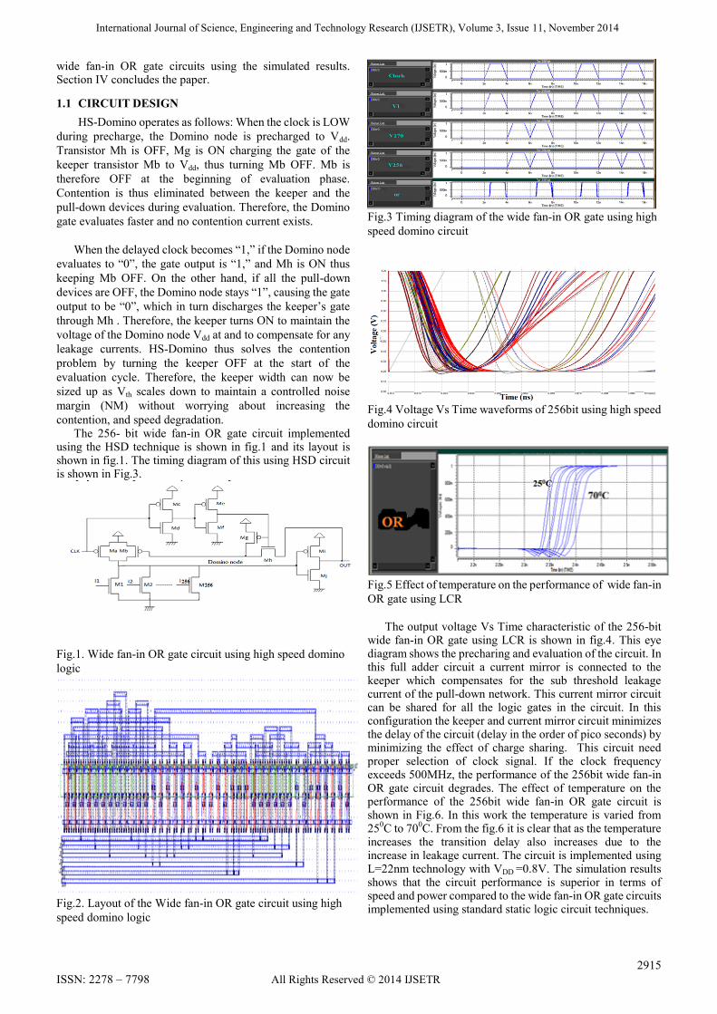
using the HSD technique is shown in fig.1 and its layout is shown in fig.1. The timing diagram of this using HSD circuit is shown in Fig.3.
Fig.1. Wide fan-in OR gate circuit using high speed domino
logic
Fig.2. Layout of the Wide fan-in OR gate circuit using high
speed domino logic
Fig.3 Timing diagram of the wide fan-in OR gate using high
speed domino circuit
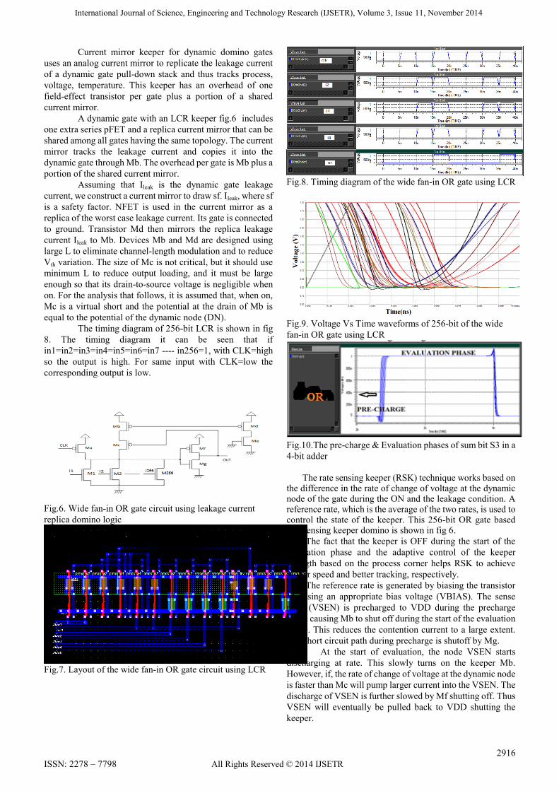
Fig.4 Voltage Vs Time waveforms of 256bit using high speed
domino circuit
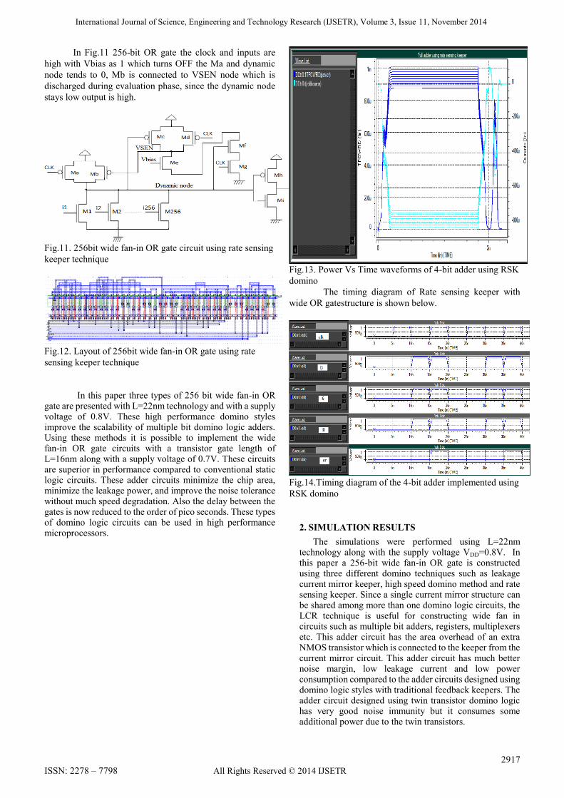
Fig.5 Effect of temperature on the performance of wide fan-in
OR gate using LCR
The output voltage Vs Time characteristic of the 256-bit
wide fan-in OR gate using LCR is shown in fig.4. This eye diagram shows the precharing and evaluation of the circuit. In this full adder circuit a current mirror is connected to the keeper which compensates for the sub threshold leakage current of the pull-down network. This current mirror circuit can be shared for all the logic gates in the circuit. In this configuration the keeper and current mirror circuit minimizes the delay of the circuit (delay in the order of pico seconds) by minimizing the effect of charge sharing. This circuit need proper selection of clock signal. If the clock frequency exceeds 500MHz, the performance of the 256bit wide fan-in OR gate circuit degrades. The effect of temperature on the performance of the 256bit wide fan-in OR gate circuit is shown in Fig.6. In this work the temperature is varied from 25
0C to 70
0C. From the fig.6 it is clear that as the temperature
increases the transition delay also increases due to the increase in leakage current. The circuit is implemented using L=22nm technology with VDD =0.8V. The simulation results shows that the circuit performance is superior in terms of speed and power compared to the wide fan-in OR gate circuits implemented using standard static logic circuit techniques.
International Journal of Science, Engineering and Technology Research (IJSETR), Volume 3, Issue 11, November 2014
2916
ISSN: 2278 – 7798 All Rights Reserved © 2014 IJSETR
Current mirror keeper for dynamic domino gates
uses an analog current mirror to replicate the leakage current
of a dynamic gate pull-down stack and thus tracks process,
voltage, temperature. This keeper has an overhead of one
field-effect transistor per gate plus a portion of a shared
current mirror.
A dynamic gate with an LCR keeper fig.6 includes
one extra series pFET and a replica current mirror that can be
shared among all gates having the same topology. The current
mirror tracks the leakage current and copies it into the
dynamic gate through Mb. The overhead per gate is Mb plus a
portion of the shared current mirror.
Assuming that Ileak is the dynamic gate leakage
current, we construct a current mirror to draw sf. Ileak, where sf
is a safety factor. NFET is used in the current mirror as a
replica of the worst case leakage current. Its gate is connected
to ground. Transistor Md then mirrors the replica leakage
current Ileak to Mb. Devices Mb and Md are designed using
large L to eliminate channel-length modulation and to reduce
Vth variation. The size of Mc is not critical, but it should use
minimum L to reduce output loading, and it must be large
enough so that its drain-to-source voltage is negligible when
on. For the analysis that follows, it is assumed that, when on,
Mc is a virtual short and the potential at the drain of Mb is
equal to the potential of the dynamic node (DN).
The timing diagram of 256-bit LCR is shown in fig
8. The timing diagram it can be seen that if
in1=in2=in3=in4=in5=in6=in7 ---- in256=1, with CLK=high
so the output is high. For same input with CLK=low the
corresponding output is low.
Fig.6. Wide fan-in OR gate circuit using leakage current
replica domino logic
Fig.7. Layout of the wide fan-in OR gate circuit using LCR
Fig.8. Timing diagram of the wide fan-in OR gate using LCR
Fig.9. Voltage Vs Time waveforms of 256-bit of the wide
fan-in OR gate using LCR
Fig.10.The pre-charge & Evaluation phases of sum bit S3 in a
4-bit adder
The rate sensing keeper (RSK) technique works based on
the difference in the rate of change of voltage at the dynamic node of the gate during the ON and the leakage condition. A reference rate, which is the average of the two rates, is used to control the state of the keeper. This 256-bit OR gate based rate sensing keeper domino is shown in fig 6.
The fact that the keeper is OFF during the start of the
evaluation phase and the adaptive control of the keeper
strength based on the process corner helps RSK to achieve
higher speed and better tracking, respectively. The reference rate is generated by biasing the transistor
Me using an appropriate bias voltage (VBIAS). The sense
node (VSEN) is precharged to VDD during the precharge
phase causing Mb to shut off during the start of the evaluation
phase. This reduces the contention current to a large extent.
The short circuit path during precharge is shutoff by Mg.
At the start of evaluation, the node VSEN starts
discharging at rate. This slowly turns on the keeper Mb.
However, if, the rate of change of voltage at the dynamic node
is faster than Mc will pump larger current into the VSEN. The
discharge of VSEN is further slowed by Mf shutting off. Thus
VSEN will eventually be pulled back to VDD shutting the
keeper.
International Journal of Science, Engineering and Technology Research (IJSETR), Volume 3, Issue 11, November 2014
2917
ISSN: 2278 – 7798 All Rights Reserved © 2014 IJSETR
In Fig.11 256-bit OR gate the clock and inputs are
high with Vbias as 1 which turns OFF the Ma and dynamic
node tends to 0, Mb is connected to VSEN node which is
discharged during evaluation phase, since the dynamic node
stays low output is high.
Fig.11. 256bit wide fan-in OR gate circuit using rate sensing
keeper technique
Fig.12. Layout of 256bit wide fan-in OR gate using rate
sensing keeper technique
In this paper three types of 256 bit wide fan-in OR
gate are presented with L=22nm technology and with a supply voltage of 0.8V. These high performance domino styles improve the scalability of multiple bit domino logic adders. Using these methods it is possible to implement the wide fan-in OR gate circuits with a transistor gate length of L=16nm along with a supply voltage of 0.7V. These circuits are superior in performance compared to conventional static logic circuits. These adder circuits minimize the chip area, minimize the leakage power, and improve the noise tolerance without much speed degradation. Also the delay between the gates is now reduced to the order of pico seconds. These types of domino logic circuits can be used in high performance microprocessors.
Fig.13. Power Vs Time waveforms of 4-bit adder using RSK
domino
The timing diagram of Rate sensing keeper with
wide OR gatestructure is shown below.
Fig.14.Timing diagram of the 4-bit adder implemented using
RSK domino
2. SIMULATION RESULTS
The simulations were performed using L=22nm technology along with the supply voltage VDD=0.8V. In this paper a 256-bit wide fan-in OR gate is constructed using three different domino techniques such as leakage current mirror keeper, high speed domino method and rate sensing keeper. Since a single current mirror structure can be shared among more than one domino logic circuits, the LCR technique is useful for constructing wide fan in circuits such as multiple bit adders, registers, multiplexers etc. This adder circuit has the area overhead of an extra NMOS transistor which is connected to the keeper from the current mirror circuit. This adder circuit has much better noise margin, low leakage current and low power consumption compared to the adder circuits designed using domino logic styles with traditional feedback keepers. The adder circuit designed using twin transistor domino logic has very good noise immunity but it consumes some additional power due to the twin transistors.
International Journal of Science, Engineering and Technology Research (IJSETR), Volume 3, Issue 11, November 2014
2918
ISSN: 2278 – 7798 All Rights Reserved © 2014 IJSETR
3.CONCLUSION
As the technology scales down, the leakage current of the pull down evaluation network increases, especially in wide fan in dynamic gates such as wide OR gates, wide AND-OR gates used in microprocessors. This will increase the power consumption and reduce the noise immunity. In this paper the performance of 4-bit adder circuit designed using three domino circuit techniques (LCR, Twin Transistor logic, and RSK) is analyzed in detail and its performance is compared with other adder circuits. The 256-bit wide fan-in OR gate circuit is simulated using L=22nm technology along with supply voltage VDD=0.8V. The experimental results shows that these wide fan in OR gate circuits gives superior performance compared to wide fan-in OR gate circuits designed using conventional domino techniques.
REFERENCES
[1]A. Alvandpour, R. K. Krishnamurthy, K. Soumyanath, and S. Y.Borkar,
―A sub-130-nm conditional keeper technique,‖ IEEE J.Solid-State Circuits,
vol. 37, no. 5, pp. 633–638, May 2002.
[2] M. Anis, M. Allam, and M. Elmasry, ―Energy-efficient noise-tolerant
dynamic styles for scaled-down CMOS and MTCMOS technologies,‖IEEE
Trans. Very Large Scale Integr. (VLSI) Syst., vol. 10, no. 2, pp.71–78, Apr.
2002.
[3] Y. Lih, N. Tzartzanis, and W. W. Walker, ―A leakage current replica
keeper for dynamic circuits,‖ IEEE J. Solid-State Circuits, vol. 42, no.1, pp.
48–55, Jan. 2007.
[4] C. H. Kim, K. Roy, S. Hsu, R. Krishnamurthy, and S. Borkar, ―A process
variation compensating technique with an on-die leakage current sensor for
nanometer scale dynamic circuits,‖ IEEE Trans. Very Large Scale Integr.
(VLSI) Syst., vol. 14, no. 6, pp. 646–649, Jun. 2006.
[5] L. Ding and P. Mazumder, ―On circuit techniques to improve noise
immunity of CMOS dynamic logic,‖ IEEE Trans. Very Large ScaleIntegr.
(VLSI) Syst., vol. 12, no. 9, pp. 910–925, Sep. 2004.
[6] H. F. Dadgour, R. V. Joshi, and K. Banerjee, ―A novel variation-aware
low power keeper architecture for wide fan-in dynamic gates,‖ in Proc.DAC,
2006, pp. 977–982.
[7] V. Kursun and E. G. Friedman, ―Domino logic with variable threshold
voltage keeper,‖ IEEE Trans. Very Large Scale Integr. (VLSI) Syst., vol.11,
no. 6, pp. 1080–1093, Dec. 2003.
[8] C.-H. Hua, W. Hwang, and C.-K. Chen, ―Noise-tolerant XOR-based
conditional keeper for high fan-in dynamic circuits,‖ in Proc. IEEE
Int.Symp. Circuits Syst., (ISCAS), 2005, pp. 444–447.
[9] H. Mahmoodi-Meimand and K. Roy, ―Diode-footed domino: A
leakage-tolerant high fan-in dynamic circuit design style,‖ IEEE Trans.
Circuits Syst., I, Reg. Papers, vol. 51, no. 3, pp. 495–503, Mar.2004.
[10] H. Nambu, K. Kanetani, K. Yamasaki, K. Higeta, M. Usami, Y.
Fujimura,K. Ando, T. Kusunoki, K. Yamaguchi, and N. Homma, ―A 1.8-ns
access, 550-MHz, 4.5-Mb CMOS SRAM,‖ IEEE J. Solid-State Circuits,
vol. 33, no. 11, pp. 1650–1658, Nov. 1998.
[11] S. Vangal, M. A. Anders, N. Borkar, E. Seligman, V. Govindarajalu, V.
Erraguntla, H. Wilson, A. Pangal, V. Veeramachaneni, J. W. Tschanz,Y. Ye,
D. Somasekhar, and B. A. Bloechel, ―5-GHz 32-bit integer executioncore in
130-nm dual-Vt CMOS,‖ IEEE J. Solid-State Circuits,vol. 37, no. 11, pp.
1421–1431, Nov. 2002.
[12] R. G. D. Jeyasingh and N. Bhat, Indian patent application 01 130/CHE/
2007, May 01, 2007.
[13] R. G. D. Jeyasingh and N. Bhat, PCT application PCT/IN2007/000 259,
Jun. 26, 2007.
[14] R. G. D. Jeyasingh and N. Bhat, ―A lowpower, process invariant keeper
design for high speed dynamic logic circuits,‖ in Proc. ISCAS, 2008,pp.
1668–1671.
RAJASRI.K received the B.E degree in
Electronics and communication engineering from AVC
college of engineering Mannampandal, Mayiladuthurai,
Tamilnadu. She is currently pursuing the M.E.degree in
Applied electronics from the IFET college of Engineering,
Villupuram, Tamilnadu. Her current research interests
include low-power,high-performance, and robust circuit
design for deep-submicrometer CMOS technologies.
MANIKANDAN.M received the B.E degree in
Electronics and communication engineering from Sri
Manakula Vinayagar college of engineering Puducherry,
India and M.E degree in Karuniya University, Coimbatore ,
India .His current research interests include low-power,
high-performance, and robust circuit design for
deep-submicrometer CMOS technologies.
BHARATHI. A was born in Tamilnadu in 1990.
She obtained the Bachelor of degree in Electrical and
Electronics Engineering with First Class Honours in
Avinashilingam University, Tamilnadu in 2012. She is doing
her M.E Applied Electronics in IFET College of
Engineering,Tamilnadu. Her current research interests
include low-power design for deep-submicrometer CMOS
technologies.