a split-drain transistor study case: measuring noise and … · 2006-07-23 · a split-drain...
TRANSCRIPT

A Split-Drain Transistor Study Case: Measuring Noise and Sensitivity
Fernando C. Castaldo and Carlos Alberto do Reis FilhoLaboratorio de Microeletrônica Magneti-Marelli
Departamento de Semicondutores e FotônicaUnicamp
AbstractThis paper introduces some briefs about Current ModeMagnetic Field Sensors and carries out a complete noiseanalysis for a basic Split-drain-based setup, showing thatthe actual model for a MOSFET transistor can be usefulfor noise calculations along with some statisticalconsiderations. It is shown that the Minimum DetectableField (MDF) is strongly dependent of the Bandwidth ofthe measurement system. Furthermore, some practicalresults are shown for validating the previous analysis.Also, a new structure currently under manufacturing isproposed as an amplifier and conditioner signal for anintegrated magnetic sensor.
INTRODUCTION.
The first magnetic field sensitive devices have beenstudied formerly based on silicon Hall Plate devices,which have very low sensitivity when compared withother semiconductors. The first magnetic-field sensitiveMOS device was the MOS Hall element proposed byGallagher and Corak [1]. The Split-Drain MOStransistor configuration of the kind proposed by Fry andHoey [2], employed a MOS transistor with diffusedprobes (drains) where an asymmetry of current flowcould be detected between the drains in the presence of amagnetic field being the device kept in saturation. A thirddrain may be used to carry the main bias currentachieving a higher sensitivity for the device. Themodeling of the device is based on Poisson Equation forthe Hall Plate and a reasonable linearity was obtained upto 8kG. Fig. 1 shows such device and the scheme usedfor detecting the current imbalance and amicrophotograph of an early device.
Fig. 1 Former Split-Drain (Fry, and Hoey)
CURRENT MODE MAGNETIC SENSORS
The term MAGFET stands for Magnetic EffectTransistor and includes all classes of devices that arebased on carriers deflection by Lorentz effect, causing animbalance of charges in voltage-mode hall devices and a
current imbalance in current-mode ones [3]. Amongstthe current mode Hall devices are the Split-Drain (SD)transistors which are of great interest due theircompatibility with CMOS process, allowing ASICsimplementation [4]. Also compatible with the CMOStechnology are the Magnetotransistors (MT), includingthe vertical and lateral parasitic bipolar transistors withdouble collector [5]. Both devices used together allows3D magnetic sensors implementation. Also, the use of aSD and two double-collector vertical bipolar parasitictransistors can be used for 3D magnetic sensors systemsimplementation with cross sensitivity minimized [6].Both devices the SD and MT are supposed to operate inHall Dual current mode exploiting the advantages ofcurrent mode signal processing, such as higherfrequencies of operation [7].
SPLIT-DRAIN MAGFET DEVICES
The great interest in MAGFETs Split-Drain transistors isthat the output response is very linear with field strength,allowing for the implementation of measurementssystems and other field-related applications where anoutput signal should track a magnetic field. At lowfrequency measurements the 1/f noise predominates, andsome limitations regarding the sensitivity can beobserved. To minimize the 1/f noise one can adopt largertransistor ratio W/L taking into full consideration thetrade-off between sensitivity, dissipated power and noise.In medium and high frequencies the thermal noise takesover. The most important parameter in characterizing theSD transistor is its sensitivity. The sensitivity of the SDMAGFET can be characterized by the fraction of thedrain current changed under the influence of a magneticfield for a specific drain bias current. The sensitivity istherefore defined by Eq. (1).
(1)
According Killat, the sensitivity of the SD depends onthe geometry and operating point and rises withincreasing the transistor ratio L/W. Also, the sensitivityis higher for the device operating in linear region.Experimental results have shown for a SD–N( 32u/48u) asensitivity S=2.33 %/T [8]. According other studies [9],the sensitivity is independent of the geometry of thedevice, but affected by the gap between drains.Furthermore, the sensitivity is limited by the Hallmobility and is insensitive to region operations.Theoretical model foresee 5,8%/T of maximumsensitivity and a experimentally SD–N(20u/200u)
S a∆I
I Q B⋅

attained 3,1%/T. This corroborates that typicalsensitivities for SD MAGFETs are less than 6%/T [10].By the other hand, Kub and Scott have shown a modifiedSD MAGFET employing multiple gates whosesensitivity of 18,5%/T is attained [11].
PHYSICS OF THE SPLIT-DRAIN MAGFET
As mentioned above the current imbalance that takesplace on a Split-Drain MAGFET under a magnetic fieldis related to Lorentz force that modifies the distributionof inversion charges along the channel of a MOStransistor [3]. The current density for a N-inversionchannel along the surface of the channel is given by Eq.(2)
(2)
In Eq. 2 µn denotes the drift mobility, n the carrierdensity, E the Electric Field, B the Magnetic Field, q theelectron charge and r the Hall scattering factor. Solving(2) numerically along with the MOS transistors equationseither in linear or saturation region, a deep insight can beobtained regarding Sensitivity, Geometric Factor andcurrent and voltage Hall as well [9]. In literature we findseveral works about the physics of interaction betweencharges and magnetic fields [12], [13], [14].
NOISE MODEL FOR THE SPLIT-DRAIN
The noise model for the Magfet Split-Drain transistorfollows the MOSFET device equations for the noise,taking into account the correlation factor between thesplit current in the drains of the device. Regarding theworst case in terms of generated total noise, the RMSnoise current per drain in a single device is given by Eq.3, where INTrms is the total noise current generated by anequivalent MOSFET transistor whose dimensions are thesame of the Magfet device.
(3)
The MOSFET noise model is based on Spectral NoiseCurrent [15] as indicated in Eq. 4. The factor K is theBoltzman constant K=1.381e-23 J/K, T is the absolutetemperature, gm is the transistor transconductance, KF isthe flicker noise factor, COX is the gate capacitance, Wand L are the MAGFET dimensions. The MOSFETsmall-signal gm transconductance is given by Eq. 5. KP isthe static transconductance of the MOSFET and IQ is thebias current. The model for the 1/f noise was based onBSIM3 model for the MOS transistor.
(4)
(5)
The spectral noise voltage can be obtained if atransconductance factor G that convert current spectraldensity into voltage spectral density is used as indicatedin Eq. 6.
(6)
The total RMS noise current and voltage can becalculated regarding the bandwidth of the range ofinterest. In a theoretical approach, Eq. 7 calculates thetotal RMS noise, either current or voltage-referred.
(7)
CHARACTERIZING THE BASIC SPLIT-DRAIN CELL
A basic split-Drain transistor was built in CMOStechnology 0,8u with dimensions W=20u, L=200u, and asetup was used to characterize the device [16]. In sucharrange an instrumentation amplifier was employed asdifferential amplifier to sense the differential current andoutput a voltage proportional to magnetic field. Fig. 2shows the basic setup. Inside the dashed box, a biasscheme was considered noiseless as first approximation,and the results have shown its validity. Additionally aoutput high-pass filter with corner frequency around0,1Hz was used in order to prevent severe 1/f noise andsome offset drift that can affect the measurements. Howthis circuit is primarily intended to measure industrialfrequencies, such limitation can be held.
Fig. 2 Basic Setup for Noise and Sensitivitymeasurements
I Nrms
I NTrms
2
SI
8 K⋅ T⋅ gm⋅
3
KF gm2
⋅
COX W⋅ L⋅ f⋅+
A2
Hz
S V
S I
G2
gm 2 KP⋅W
L⋅ IQ⋅
A
V2
VRMS0
∞
fSV⌠⌡
d IRMS0
∞
fSI⌠⌡
d
J n
q n⋅ µ n E→⋅ r µ n⋅ B
→E
→×( )⋅+
⋅
1 r µ n⋅ B→
⋅
2+
I NT
2
I NT
2
I NT
Noiseless
B
AD620

The basic equation for the circuit reads:
(8)
The new parameter introduced here is the transferfunction of the instrumentation amplifier H( ). TheInstrumentation amplifier used was the Analog Devices’AD620. The resistor R is the equivalent output resistanceof the I-V converter. In this case, simple resistors areused to perform such conversion. Fig. 3 shows the basiccircuit for determining the total noise generated by thesplit-drain. The simplified model adopted here was tosplit the MAGFET current spectral density from thecalculated value for the MOSFET with same dimensions.The differential scheme also includes an extra noise, duethe fact of non-correlated noise signals being applied toamplifier inputs and due the presence of converter I-Vresistors as well.
Fig. 3 Model for Noise Calculations
The Noise voltage at the output of the circuit in Fig.3 isgiven by Eq. 9. SI is the noise current spectral density,G is the I-V converter transconductance (R=100K) andH( ) is the transfer function of the AD620 amplifier.The differential operation carried out by the amplifierdoes not reduce the noise generated by each arm aswould do for a differential scheme. Instead, these noisesources adds up by a factor of √2 if non-correlatedsignals are considered. Another important point to benoted is the bandwidth of both the I-V converter andamplifier used. The larger the bandwidth, the grater theoutput RMS noise.
(9)
Some additional noise generated by the AD620 itself canbe also accounted for the total noise, taking the quadraticmean value and referring to the output circuit. This isdone by Eq. 10.
(10)
NOISE CALCULATIONS FOR THE BASIC SETUP
Following the noise calculation procedure above andconsidering the basic setup indicated in Fig. 2, the circuitparameters read:
Transistor Split Drain PMOSAMS CYB 0,8u TechnologyKP=31 uA/V2 VTH=0,85V COX=2.16fF/u2
Size: W=20u L=200uBias: IS=15 uA VGS=4,5V gm=8,12 uA/VID/2 =7,5 uAFlicker Noise Coeficient: KF=6.31E-29 V2FRelative Sensitive: 0.6%/T
AD620 Corner Frequency and Spectral DensitySetting a gain of 1000 (60dB) the following parametersare obtained from the AD620 datasheet [datasheet]:√S=9 nV/√Hz input-referred (Low Noise )G=1000fc=12KHZ Roll-off=-20dB/dec
Thus a simplified model for the frequency dependentcharacteristic of the AD620 can be drawn, as indicatedby Eq. 11.
(11)
Applying Eq. 9 the total noise can be obtained.
The total noise generated by the AD620 amplifier isoutput-refereed, taking into account the noise spectraldensity, √S=9 nV/√Hz and integrating over the frequencyrange of interest.
The total noise measured at output of the system is thequadratic mean of both the split-drain-transistor–IVconverter and Instrumentation amplifier.
A feasible approach to check out the RMS value of thenoise generated by a circuit is carried out by a digitaloscilloscope such as Tektronix TDS series. In suchapproach, the RMS value is calculated by squaring thedifference between the acquitted values and their
VNrms 2
0
∞
fS I
24 K⋅ T⋅ G⋅+
R2
⋅ H 2 π⋅ f⋅( )( )2⋅
⌠⌡
d⋅
VNTrms V Nrms2
V NAD6202
+
=9.07mV (RMS)
0
∞
f9 109−
⋅( )2H 2 π⋅ f⋅( )( )2
⋅
⌠⌡
d 1.23m
9.07 10-3
⋅( )21.23 10
3−⋅( )2
+ 9.153 103−
×=
(V RMS)
2
0
∞
f1
2
8 K⋅ T⋅ g m⋅
3
6 1025−×
f+
⋅ 4 K⋅ T⋅1
R⋅+
R2
⋅ H 2 π⋅ f⋅( )( )2⋅
⌠⌡
d⋅
V (RMS)
V out f( ) R ∆I⋅ H 2 π⋅ f⋅( )⋅ R S a⋅ I Q⋅ B⋅ H 2 π⋅ f⋅( )⋅:=

medium value taken from an interval of measurementand summing them up. The final value is divided by thetotal number of measured points and over this value istaken the root square. The base time of the scope has noinfluence over this procedure.
NOISE MEASUREMENTS
As proposed by Killat the basic setup for noise andsensitivity measurements was implemented taking extracare in shielding and grounding the circuit properly tominimize errors in readings. Applying such scheme [8],the total noise generated by the Split-Drain basic setupand measured by using the Oscilloscope is around12mVRMS The difference between the calculated noiseand measured one is due the noise-less parts of the circuitnot considered in analysis and the resistor-based biascircuit not taken into account as well. Applying Eq. (8)the equivalent magnetic field noise is calculated andreferred to a 1T magnetic field input and can be plottedas relative units dB. In Fig. 4 the total output noise isplotted as absolute value for a resolution bandwidth of0,25 Hz. The 1T magnetic field relative measurement isgiven by Eq. 12. The proposed setup have show a relativemagnetic noise field of –64.5 dB relative a 1T appliedfield at 1Hz frequency and 1Hz bandwidth. Ascomparative purposes, Killat have shown –80dB forsame conditions. For 60Hz, the magnetic noise is –88,8dB. This means that if we were able to detect a magneticfield using a 1Hz ideal bandwidth filter at 60Hz, theproposed setup plus the ideal filter would be capable ofsensing a magnetic field of -88,8dB or 36,3uT.
(12)
Fig. 4 Magnetic Noise Measurements
THE MINIMUM DETECTABLE FIELD- MDF
According Lau, the Minimum Detectable Field (MDF)in a Split-Drain MAGFET is related to the Sensitivityand Bias Current and proportional to Sa
–1 IQ-3 / 2 . For
instance, the MDF for a MAGFET Split-Drain transistoroperating at 60mA bias current and 30MHz frequency is1mT [10]. However, the MDF is strongly dependent ofthe bandwidth of the instrumentation system. Thereforethe bandwidth of the instrumentation amplifier AD620and I-V converter in basic setup will have importantinfluence on the MDF. Another I-V conversions schemesapply as well. The minimum magnetic detectable field isdefined in theory when the RMS value of the field beingdetected equals the total noise generated by themeasurement system. Thus, combining Eq. 8 and 9, andsolving for the bias current and I-V converter resistor,one can check out the minimum detectable magnetic fieldsignal numerically. As indicate in Fig. 5 the MDF issome dependent of the I-V converter impedance.
Fig. 5 Calculated MDF Figure
For the specified conditions when R=100K andIQ=15uA, the MDF=1.6mT read from Fig. 5. This valuewas scaled for a peak value, considering a sinusoidalvariation of the applied magnetic field. In practice, valuesslightly above this inferior limit will be registered due theapproximations considered. For the proposed basic setupthe MDF measured is around 1,7mT, a good agreementwith the 1,6mT calculated and read from Fig. 5. Also, forsimplifying calculations purposes, the instrumentationamplifier noise was not taken into account for the MDFof the circuit.
NOISE FACTOR
Considering a Gaussian Distribution for the Noise andthe calculated total output RMS noise voltage, whatwould be the expected maximum noise peak to happen ?From such distribution, the total noise RMS outputvoltage is given by its standard deviation σσ [17]. Theaverage noise value is zero for such distribution. Here weassume that the predominant noise effect on the
@ 60 Hz
R=100K
R=1M Measured
[uA]
[T]
MDF
dB 20 log2V RMS
R I Q⋅ S R⋅ H⋅
⋅
MAGFET transistor is due the thermal one regarding thefrequency range of interest. Taking into account theprobability of peak noise value occurrence, Eq. 13shows this probability as a function of the specific noisepeak value (noise) and the standard deviation of suchdistribution. The erf function is the classical given by Eq.14.
(13)
(14)
Two points are of particular interest in such Gaussiandistribution when applying Eq. 13. The probability ofoccurrence of 42,5%, when the noise peak reaches thevalue equal to the average absolute value, given by Eq.15 and the probability of occurrence of 4,6%, when thepeak noise reaches twice the RMS value. Fig. 6 shows ina unity standard deviation distribution the peak noisevoltage for both situations.
(15)
Fig. 6 Peak Noise Occurrence
Regarding other frequency of peak-noise-to-RMS-value-related occurrence, Fig. 7 shows the Noise Factor.
Fig. 7 Peak-Noise Factor
In practice, as long as the measuring system is directlyaffected by the peak noise, a tradeoff should be assumedbetween the tolerable peak-noise occurrence frequencyand the Minimum detectable field (MDF). Taking thepeak-noise factor into consideration and recalculating theMDF for the setup, one can observe that the MDF isreduced by the noise factor (NF) as indicated by Eq. 16.
(16)
MEASUREMENTS OF MAGNETIC FIELDS
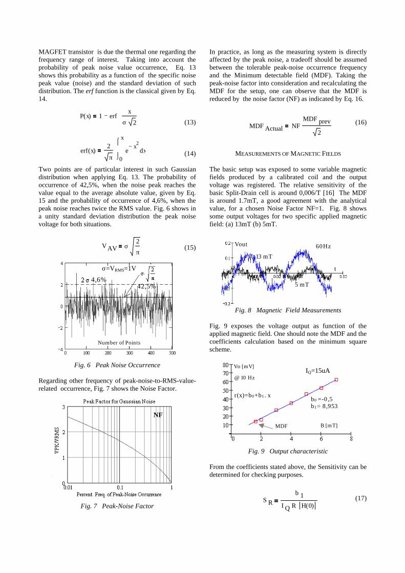
The basic setup was exposed to some variable magneticfields produced by a calibrated coil and the outputvoltage was registered. The relative sensitivity of thebasic Split-Drain cell is around 0,006/T [16] The MDFis around 1.7mT, a good agreement with the analyticalvalue, for a chosen Noise Factor NF=1. Fig. 8 showssome output voltages for two specific applied magneticfield: (a) 13mT (b) 5mT.
Fig. 8 Magnetic Field Measurements
Fig. 9 exposes the voltage output as function of theapplied magnetic field. One should note the MDF and thecoefficients calculation based on the minimum squarescheme.
Fig. 9 Output characteristic
From the coefficients stated above, the Sensitivity can bedetermined for checking purposes.
(17)
P x( ) 1 erfx
σ 2⋅
−
erf x( )2
π 0
x
xex
2−⌠⌡
d⋅
V AV σ2
π⋅
S R
b 1
I Q R⋅ H 0( )⋅
MDF Actual NFMDF prev
2⋅
σ=VRMS=1V
4,6%42,5%
Number of Points
NF
13 mT
5 mT
Vout
t
60Hz
B [mT]
Vo [mV]
@ 10 Hz
r(x)=b0+b1 . xb0 =-0,5b1 = 8,953
MDF
IQ=15uA

The calculated value agree with that determined byJimenez, S=0,6 %/T [16]. Fig. 10 also shows the bias-dependence of the output voltage as function of appliedmagnetic field.
Fig. 10 Bias-Dependence Output characteristic
Regarding the applied magnetic field frequency, Fig.11shows the output voltage as function of frequency for afixed applied magnetic field B=5mT. In the proposedbasic setup the flat response reaches up to 1KHz, abovethat, a parasite induction takes place, raising the outputresponse.
Fig. 11 Field Frequency Output Voltage
The parasitic output voltage induction is astraightforward application of Faraday Law as long as theleads of the SD transistor perform a loop, whose signalinduced is amplified by the high-input-impedanceinstrumentation amplifier. Fig. 12 shows the inducedoutput voltage for the loop comprised by the integratedcircuit leads.
Fig. 12 Loop Induction
A possible approach to minimize such effect is toimplement low-impedance paths for the field-sensitivecurrents. That is the Current Mode Processing does [7].Furthermore, one can reduce the parasitic loops byproperly layout techniques.
PSPICE-BASED MODEL
The Pspice modeling does not take into account themagnetic field. So, in order to model devices whoseparameters are magnetic fields related, one should adoptthe electric equivalence approach [8], [18]. As proposedby Liu the SD MAGFET can be seen as a couple ofMosfet each one having a half area [18]. This model alsotake into account the noise model as proposed in thiswork. Fig. 13 shows the proposed model, where linearcontrolled sources perform the bias sensitivitydependence modeling. The magnetic field is simulated bymeans of an input voltage with 1V/T ratio.
Fig. 13 (a) Pspice Model (b) Equivalent
INTEGRATED ARCHITECTURES
The use of Split Drain MAGFET arrays for improvingthe sensitivity and performance of magnetic sensors iswell know in literature. Such arrays are generallycomposed by the SD transistor and some active load suchas NMOS or PMOS current mirrors, performing a basiccell [19]. Using the transistor area scaling in a simple orcascode mirror, the SD MAGFET output current isamplified by this scale factor. Thus, the total deviationoutput current is given by the all contributions ofindividual cells, achieving higher sensitivities. However,the noise can propagate the same way and be amplifiedas well. The noise propagation is the real limitation ofsuch approaches. Other structures perform a direct I-Vconversion by employing two complementary SDtransistors, a N-type and a P-type [20]. In this work the
etφ t( )d
dA LOOP t
Bd
d⋅
BVo=e.H(w)
e
Vo [mV]
f [KHz]
B=5 [mT]
Aloop.dφ/dt. H
VP
VP
B (1V/T)
G=1
G=Sr
S
D1 D2
D1 D2
W/2LW/L
S
(a) (b)
IQ=10,2 uA
IQ=14 ,3 uA
IQ=18 uA
@ 60 Hz

following structure Fig. 14 is proposed as magnetic fieldsensor basic cell.
Fig. 14 Current Area-Scaled Amplifier
The area-scaled transistors produce the required gain forthe SD output imbalance current. The required gain canbe achieved either choosing another area ratio orcascading multiple cells. In the later case, using 3 cells,60dB of current gain can be achieved. The use ofcascode structures also improves the output characteristicof the cell. Due the low impedance paths, the cell can beoperated at high frequencies. This structure is undermanufacturing process. Simulation results have shown aMDF of around 500 µT if a adequate capacitor-basedcompensation scheme is adopted.
CHIP MICROPHOTOGRAPHY
Fig. 15 shows the Microphotography of the basicMAGFET Split-Drain (W=20u L=200u) and Fig. 16shows the basic setup used for characterizing themagnetic sensor.
Fig. 15 Split-Drain Microphotography
References
[1] Gallagher, C., Corak, W.S. Solid State Electronics, vol. 9, pp. 571-580, 1966.
[2] Fry, P.W., Hoey, S.J., A Silicon MOS magnetic field transducer ofhigh sensitivity. IEEE Transaction on Electron Devices, vol. ED-16, pp35-39. 1969.
[3] Popovic, R.S. Hall Effect Devices. The Adam Hilger Series onSensors. ISBN 0-7503-0096-5. 1991.
[4] Reis, C.A. Split drain based circuit for Measuring electric Power.IEEE Proceedings. .....
[5] Galeazzo, E. Sensores de Campo Magnético compatíveis comcircuitos Integrados. Dissertação de Mestrado. Escola Politécnica-USP.SP. 1993.
[6] Misra, D. Zhang, M. A Novel 3-D Magnetic Field Sensor inStandard CMOS Technology. IEEE Proceedings 1991.
[7] Toumazou, C. et al. Analogue IC design. The Current ModeApproach. ISBN 0863412971. 1990.
[8] Killat, D. et al. Measurement and Modeling of Sensitivity andNoise of MOS magnetic field –effect transistors. Sensor and Actuators.A61. 1997. Pp-345-351.
[9] Lau-2, J. et al. Modelling of Split-Drain magnetic field-effecttransistor (MAGFET). Sensors and Actuators. A49. Pp. 155-162.
[10] Lau, J. et al. Minimum Detectable Signals of integrated magneticsensors in bulk CMOS and SOI technologies for magnetic read heads.Sensors and Actuators. A54. 1996. Pp. 636-640.
[11] Kub, F.J., Scott, C.S. Multiple Gate Split-Drain MOSFETmagnetic field sensing device and amplifier. Tech. Digest. IEEEInternational Electron Devices Meeting. 1992.
[12] Nathan, A., Baltes, A et al. Modeling of a Dual-Drain NMOSMagnetic Field Sensor. IEEE journal of Solid State Circuits, Vol. SC-20. N.3. June-1985.
[13] Nathan, A., Baltes, A et al. Two-Dimensional Numerical Analysisof a Silicon Magnetic Field Sensor. IEEE transactions on ElectronDevices. VOL. ED-31. July-1984.
[14] Nathan, A., Baltes, A et al. Numerical Modeling of SiliconMagnetic Field Sensors: Magnetoconcentration Effects in Split MetalContact Devices. IEEE Transactions on Magnetics, Vol. Mag-20, N.5.Sep-1984.
[15] Allen, P., E., Geiger, R.L., Strader, N.R. Design Techniques forAnalog and Digital Circuits. McGraw Hill. 1990.
[16] Jimenez, H.R. Contribuição no estudo do Tranbsistor MOS Split-Drain como Sensor de Campo Magnético. Tese de Mestrado.UNICAMP. 1999.
[17] Bennet, W., R. Introduction to Signal Transmission-Electrical andElectronic Engineering Series. Mc Graw-Hill. 1970.
[18] Liu S.I. et al. SPICE Macro Model for MAGFET and itsApplications. IEEE Transactions on Circuits and Systems II. Analogand Digital Signal Processing. Vol. 46. N. 4. April 1999.
[19] Misra, D. A Novel CMOS Magnetic Field Sensor Array. IEEEJournal of Solid State Circuits, Vol. 25. N.2. April-1990.
[20] Popovic, R., Baltes, H. A CMOS Magnetic Field Sensor. IEEEJournal of Solid State Circuits, Vol. SC-18. N. 4. Aug. 1983.
IQ
A 10.AA10.A
A11.A2.A11.A
IQ + 10.∆IIQ - 10.∆I
IQ + ∆IIQ - ∆I
Fig. 16 Magnetic Field Application Setup